Embed Size (px)
Citation preview
ANALOGDEVICES fAX-ON-DEMAND HOTLINE - Page 2
rill ANALOGW DEVICES
I
FEATURESComplete with High Accuracy Sample/Hold and
AiDConverterDifferential Nonlinearity: :: 0.002% FSR max
IDAS1153)Nonlinearity: DAS1152: ::0.005% FSR max
DAS1153: ::0.003% FSR maxLow Differential Nonlinearity T.C.: ::2ppmrc maxHigh Throughput Rate: 25kHz mln (DAS1152)High Feedthrough Rejection: -96dBByte-Selectable Tri-State Buffered OutputsInternal Gain BeOffset PotentiometersImproved Second Source to AID/AIM824 and
AID/AIM825 ModulesAPPLICATIONSProcess Control Data AcquisitionAutomated Test EquipmentSeismic Data AcquisitionNuclear InstrumentationMedical InstrumentationRobotics
GENERAL DESCRIPTIONThe DAS1152/DAS1153 are 14-/15-bit sampling analog-to-digitalconverters having a maximum throughput rate of 25kHz/20kHz.They provide high accuracy, high stability, and functionalcompleteness all in a 2" x 4" x 0.44" metal case.
Guaranteed high accuracy system performance such as nonlinearityof ::0.005% FSR (DAS1l52)/:tO.003% FSR (DAS1l53) anddifferentia! nonlinearity of :to.003% FSR (DAS1l52)/:tO.OO2%FSR (DAS1l53) are provided. Guaranteed stability such asdifferential nonlinearity T.C. of :t 2ppml"C (DAS 1153)maximum,zero T.C. of :t80f.l.VI"Cmaximum, gain T. C. of :t8ppmt'Cmaximwn and power supply sensitivity of :to.ool% FSR/% Vsare also provided by the DAS1l52/DASllS3.
REV.AInformation furnished by Analog Devices is believed to be accurate andreliable. However, no responsibility is assumed by Analog Devices for itsuse, nor for any infringements of patents or other rights of third partieswhich may resultfrom its use.No licenseis granted by implication orotherwise under any patent or patent rights of Analog Devices.
14-Bit& 15-BitSamplingAnalog-to-DigitalConverters
DAS1152/DAS1153I
FUNCTIONAL BLOCK DIAGRAM
REf OUT
~I f,."SUO
ANAlOO
{:INPUT
.TRI.
STAtESUffERS
MS...aaliT 2BIT,81f.Ilf .elf .81f 1
La E""SlE
SIH OUTPUT
'5IM INPUT
fRl.STATf
",,"ER'
BIT .alT'BIT ,.BIT 11Bl1 11BIT nalT ,. '"58 FOR DAS,,521BIT ,. (LSS FOROAS"O31
+W+15VIAN"'-DO .. DIGITAL QNOS
__AR..!.!:~~c:!"~~"!!.A~L!.! DIGITAL GND
-ISV
,.". ut ,s THE ANALOG $!GHAl IHPUT IF TH.",""HAl "<OLOAMPt."". ISUSEO.
The DASl1S2/DASlIS3 make extensive use of both integratedcircuit and thin film components to obtain their excellentperformance, small size, and low cost. The devices contain aprecision sample/hold amplifier, high accuracy 14-/15-bit analog-to-digital converter, tri-state output buffers, internal gain andoffset trim potentiometers, and power supply bypass capacitors(as shown in Figure 1).
Four analog input voltage ranges are selectable via user pinprogramming: 0 to + 5V, 0 to + lOV, :t 5V, and :t lOV. Uni-polar coding is provided in true binary format with bipolarcoding displayed in offset binary and two's complement.Tn-state buffers provide easy interface to bus structuredapplications.
One Technology Way, P.O. Box 9106, Norwood, MA 02062.9106. U.S.A.Tel; 617/329.4700 Fax; 6171326.8703 Twx; 710/394-6577Telex: 924491 Cable: ANALOG NORWOODMASS
.
-- - --- --
OBSOLETE
ANALOGDEVICES fAX-ON-DEMAND HOTLINE - Page 3
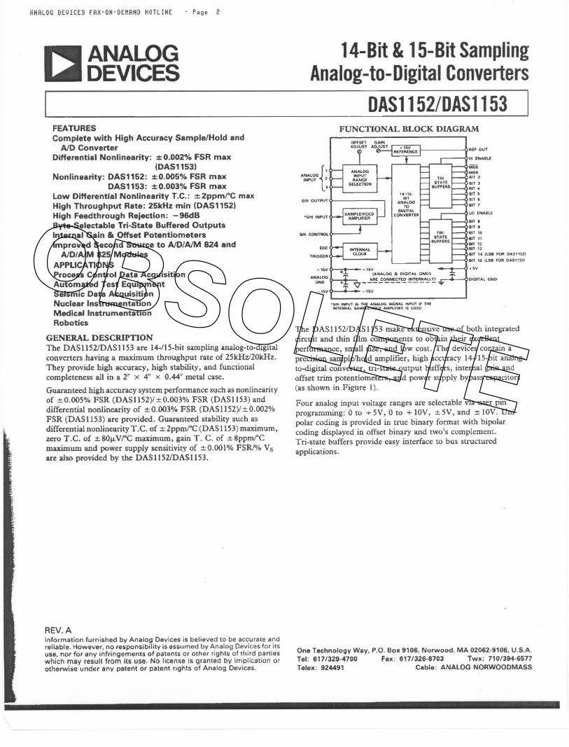
DAS1152/D~S1153-SPECIFICATIONS(typical@ +25OCunlessotherwisespecified.)DASl152 DAS1l53 OUTLINE DIMENSIONS14Bits l5Bi", Dimensions shown in inches and (mm).
MODEL
RESOLUTION
DYNAMIC PERFORMANCEThrougbput !tateConversion Time5tH Acquisition TimeSIR ApeffU", DelayStH Apenure UncertaintyFeedtbrough RejeclionIDroop RateDielectric Absorption Error
ACCURACYIntegral Nonlinearity2Differential NonJinearityNo MissingCodes:t30'Noise(S/H plus AID):t30'Noise(AID)
STABILITYDifferential Nonlinearity T.C.GainT.C.aroT.C.PowerSupply Sensitivity
ANALOG INPUTVoltage Range
BipolarUnipolar
ADCInputlmpedanceOto +5VOto+IOV,:dV:tIOV
SIR Input ImpedanceDIGITAL INPUTS
Convert Command'
StH Control
Low Enable, High Enable
DIGITAL OUTPUTSParalld Data Outputs
UnipollrBipolarOutput Drive
StatUsOutpUt Drive
INTERNAL REFERENCE VOLTAGEExternal Load Current (Rated Performance)Temperature Stability
POWER REQUIREMENTSRated VoltagesOpentingVoltages'SupplyCurrent Drain:!: 15V
+SV
TEMPERATURE RANGESpecifiedOperalingStorageRelativeHumidityShielding
SIZE
25kHzmin
35j.1.Smax4fLSMaXSOnsIns-%dB
O.OS...V/ (O.Ij..Vlj.l.Smax)!; 0.005% oflnput Voltage Change
;I:0.005% FSR'max:!:0.003%FSR'maxGuaranteed
75..Vrms50.. V rms
:!:2ppmrcmax:!;8ppml"Cmax:!:30fLvrCtyp, .!:gO...vr'Cmax:to.ool%FSR'Io/. V,
:t5V, :!:IOVOto+5V,Oto+IOV2.51d15kO10.OkOlooMniSpF
ITTL Load, Positive PulseNegative Edge TriggeredHOLD ~ LogicOSAMPLE - Logic IENABLE -LogkO
BinaryOffset Binary,2'. CompJemem2TTLLoad.Logie "I" During Conversion2TTLLoads
+IOV,:1:0.3%2mAmax:!:Sppmrcli1U
:t15V(:t:3%),+5V(:!:5%) .:t12Vto+I7V,+4.75Vto+S.25V .:t37mASOmA
010 + 7O"C
-25"Cto + 8S'C-25"Clo +85"C .Mccts MIL.STD-202E, Method 103B .Electrostatic (RFI) 6Sides, .Electromagnctic(EMI) 5Sides
2" X 4" x 0.44' MctalPackage
20kHzmin44j.1.SmaxS max.
:to.003% FSRJrnax:!:0.002% FSRJmax
.
..
NOTES'Spc<ifi<8<iom-- os DhSI152'M...u~ in hold mode. In"", lOVpk-pIo.~ tWI1.>w .u...,...;... c{SIt{and AID ...Ii...,;" enon.'fSR FuDSeal<Rana<.'Whe. e.lIN:<tincIheCoo.." C,omnw>d...dlhe SIH e roIle""iIIa!>,..."htt. Ihe p.""..idlh muStbe to". enou.. fur "'" smamplif.., '" ""qui... Ihe i.p., 110lbe requi,.,j ""'.my .", (mu. nASIIS2)!5... (mu. nhSll~3). If Ih. NO ",.vmeri. onlyuS«!, the eon , Commandpo'" ..;dlh ohouIdbe 1_. <- Fi8>JreZ}.
'If only ,be AOC """'" is WItd.II><OJICtOWc""""' IIUPJ'i>'vo!Iqe an be inod"' '" I2V,. '" tTV.Bul ;f w SIt{sect """!oirc<l.1MopmIdua moll be maiDllliDed.,"ISV <,,3%}0.-;be SIH iopu,..I,... mUl'be - ,. -TV,. -+IOVf., . " 12Vsupply...11..
'R tIIdcdPowerSol'l'iy:huloi nevUs Model923.
SpKifl<OIion$...biecl t. ehana<"nhou' notke.
NONCONOUCTI\IE lABEl
,G.'" ........"A"""A.D B""""GOLDnA TED"nL""-' ~T
1--,'-'. I':J.O~t ~U. ,,;;-~c
'_02 110>.11
.-- ,..-..
TOPV-'f"" MOo" "" - ." " "SO"
UfOIIMOonDAB""."".. "'B'eASO IS NOT HOIlMET1CAU.V SO ,
~ 1--0_1("""'."
ASSEMBLY INSTRUCTIONSCAUTION: This module is not an embedded assembly and isnot hermetically sealed. Do not subject to a solvent or water-washprocess that would allow direct contact with free liquids or vapors.Entrapment of contaminants may occur, causing performancedegradation and permanent damage. Install after any clean/washprocess and then only spot clean by hand.
~--
REV. A-2-
"';TO<............
"N I:J L P:t osv
T-., GA'" -'IV
om ,OJ ,OJ _"NO..s. Am INI
:
ANA""-."REfOOT51"OOT 1.0>
.. ' ...,N "',0'
. s.. ..&\B' !:::mBn .B,.Br> 8fT ,. (LSB ..
OBSOLETE
ANALOGDEVICES fAX-ON-DEMAND HOTLINE - Page ~
ApplyingtheDAS1152/DAS1153OPERATIONThe DASlI52/DAS 1153are functionally complete data acquisitionsubsystems being fully characterized as such. All the necessarydata acquisition and microprocessor interface elements areprovided internal to these devices. Accuracy and performancecriteria are tested and specified for the entire system. Thus,design time and associated high accuracy problems are minimizedbecause layout and component optimi7A1tionhave already becnperformed.
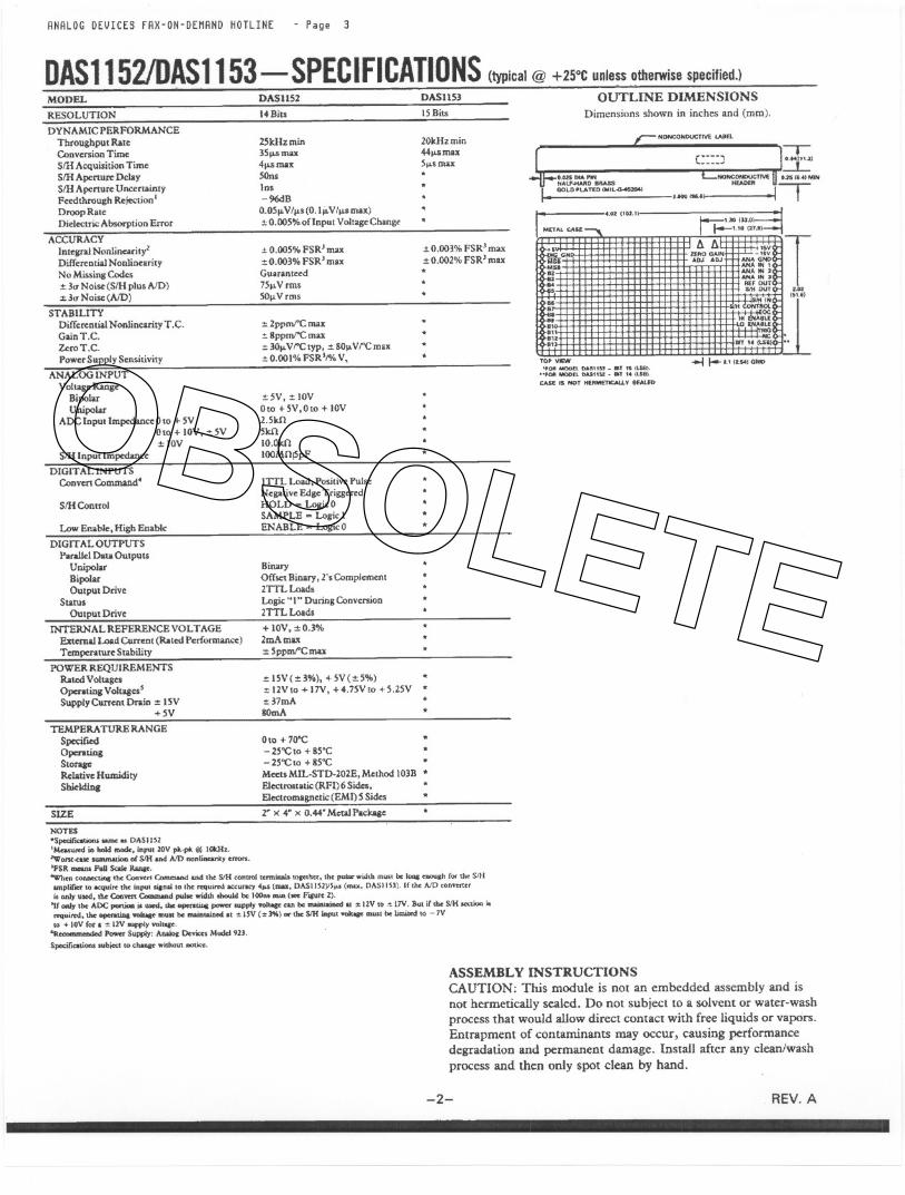
For operation, the only connections necessary to the DASl1521DAS1l53 are the :t: 15V and + 5V power supplies, analog inpUtsignal, trigger pulse, and the HI.ENABLE/LO-ENABLE tri-state controls. Analog inpUt and digital output programming areuser selectable via external jumper connections.ANALOG INPUT SECTIONThe analog inpUt can be applied to just the AID converter or tothe internal sample/hold amplifier ahead of the AID converter.When using just the AID converter, apply the analog input perthe voltage range pin programming shown in Table 1. Whenusing the sampleJhold amplifier in conjunction with AID con-verter, apply tbe analog input to the SIR INPUT terminal andconnect the S/H OUTPUT terminal to tbe appropriate AIDconverter analog input.
Table I. Analog Input Pin Programming
'NOConncctiOD
Errors due to source loading arc eliminated since the sample/holdamplifier is a high-impedance unity-gain amplifier. Highfeedthrough rejection is provided for either single-channel ormultichannel applications. Feedthrough rejection can beoptimized, in multichannel applications, by changing channelsat the rising or falling edge of the S/H control pulse.
REF OUT GAINADJUSTr------.I
II CONNECTI FORI BIPOlARIOPERATIONIIL- ,
ANA IN 1
ANA IN Z ANA1.OGINPUTRANGE
SELECTIONANA IN 3
SIH OUTPUT
SIH INPUT
51H CONTROL
Figure 2. Analog Input Block Diagram
REV. A
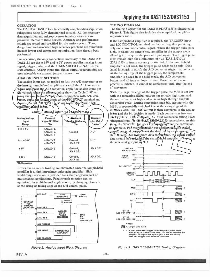
TIMING DIAGRAMThe timing diagram for the DASllS2/DAS1l53 is illustrated inFigure 3. This figure also includes the samplc/hold amplifieracquisition time.
If the sample/hold amplifier is required, the TRIGGER inputand S/H CONTROL terminal can be tied together providingonly one conversion control signal. When the trigger pulse goeshigh, it places the sample/hold amplifier in the sample modeallowing it to acquire the present input signal. The trigger pulsemust remain high for a minimum of 4fLS(DASl152)/5fLS(DAS 1153) to insure accuracy is attained. If the sample/holdamplifier is not used, the trigger pulse needs to be onJy lOOns(min) in length to satisfy the AID converter trigger requirements.At the falling edge of the trigger pulse, the sample/holdamplifier is placed in the hold mode, the AID conversionbegins, and all internal logic is reset. Once the conversionprocess is initiated, it cannot bc retriggered until after the endof conversion.
With this negative edge of the trigger pulse the MSB is set lowwith the remaining digital oUtputs set to logic high state, andthe status line is set high and remains high through the fullconversion cycle. During conversion each bit, starting with theMSB, is sequentially switched low at the rising edge of theinternal clock. The DAC output is then compared to the analoginput and the bit decision is made. Each comparison lasts oneclock cycle with the complete l4-/15-bit conversion taking 35fLSI44fLSmaximum for the DAS1l52/DASl153 respectively. At thistime, the STATUS line goes low signifying that the conversionis complete. For microprocessor bus applications, the digitaloutput can now be applied to the data bus by enabling the tri-state buffers. For maximum data throughput, the digital outputdata should be read while the samplc/hold amplifier is acquiringthe new analog inpUt signal.
TRIGGER!r-1SIH CONTROL.J t.
.
INPlJT +FS-r-+SIGNAL -~ J=:-I,+F5~SlH OUTPUT 0 - -:-fS -,
""""" ~ n n nCI.OCK T-J L..IL..IL..-
EOC 35 I\IIAX( ~~44,.. I\IIAX(0~~~:~1--t.-
MSB ==~lJ SS ~ '
81T 2 =~~~s - '
IIIT3:==~~S -,'I I tI I I II I I I
lilT 14 I 17-) ~ILSB FOR DASH52I L..J 'Wff$ 1
lilT 15 ---] $$---, VJ1IJ7JJIlSIl FOR0.0.511531__- L WQmNOTES
~ ,. Output Data Va"d.. 2, If SIH Cont...1 and Trll19ar 8<. ""d tagathr, Pul... Widthmust be 4".10.0.51152)15"0 (nASU531 m!n to allow the SIHAmplifier to acquire the Input Signal, II the ADC is onlyused, the T,11Ige, Pulse must be 100n. min.
Figure 3. DA$1152/DA$1153 Timing Diagram
-3-
-~-~
AAalogVoltage Connel:t Connect ConnectInput VINor S/H Out Analog Common Ref OutRange To To To
Oto +:5V ANA IN I,ANAINZ, Ground NC*ANAIN3
Oto + IOV ANAIN2 Ground NC*ANAIN 3 ANA IN 1
:!:5V ANA IN 1 Ground, ANAIN 2ANA IN 3
:!:JOV ANA IN 3 Ground, ANAIN2ANAJN1
OBSOLETE
ANALOGDEVICES fAX-ON-DEMAND HOTLINE - Page 5
DAS1152/DAS1153
GAIN AND OFFSET ADJUSTMENTThe DAS1l52/DAS1l53 contain internal gain and offsetadjustment potentiometers. Each potentiometer has ampleadjustment range so that gain and offset errors can be trimmedto zero.
Since offset calibration is not affected by changes in gaincalibration, it should be performed prior to gain calibration.Proper gain and offset calibration requires great care and theuse of extremely sensitive and accurate reference instruments.The voltage standard used as a signal source must be very stableand be capable of being set to within :t l/IOLSB of the desiredvalue at any point within its range.
OFFSET CALIBRATIONFor a 0 to + 10V unipolar range set the input voltage preciselyto + 305J.1.Vfor the DAS1l52 and + 153J.1.Vfor the DASlI53.For a 0 to +5V unipolar range set the input to + 153j.LVfor theDAS1l52 and + 16J.1.Vfor the DAS1l53. Then adjust the zeropotentiometer until the converter is just on the verge ofswitching from 000 000 to 000 '001.
For the :t SV bipolar range set the input voltage precisely to+305J.1.Vfor the DAS1l52 and + 153J.1.Vfor the DAS1I53. Fora :t IOV bipolar range set the input voltage precisely to + 61OJ.I.Vfor the DAS1152 and +30SJ.l.Vfor tbe DAS1153. Adjust thezero potentiometer until the offset binary coded units arc juston the verge of switching from 000 000 to 000 001and the two's complement coded W1itsare just on the verge ofswitching from 100 000 to 100 001.
GAIN CALIBRATIONSet the input voltage precisely to +9.99909V (DASllS2)1+ 9.99954V (DAS1I53) for tbe 0 to + 10V units, +4.99954V(DAS1l52)/+4.99971V (DAS1l53) for 0 to +SV units,+9.99817V (DASllS2)/+9.99909V (DAS1l53) for :t JOVunits, or +4.99909V (DASllS2)/+4.99954V (DAS1l53) for:t 5V W1its. Note that these values are I 1/2LSBs less tbannominal full scale. Adjust the gain potentiometer until binaryand offset binary coded units are just on the verge of switchingfrom 11 10 to 11 11 and two's complement coded unitsare just on the verge of switching from 011 10 to 011 .11.
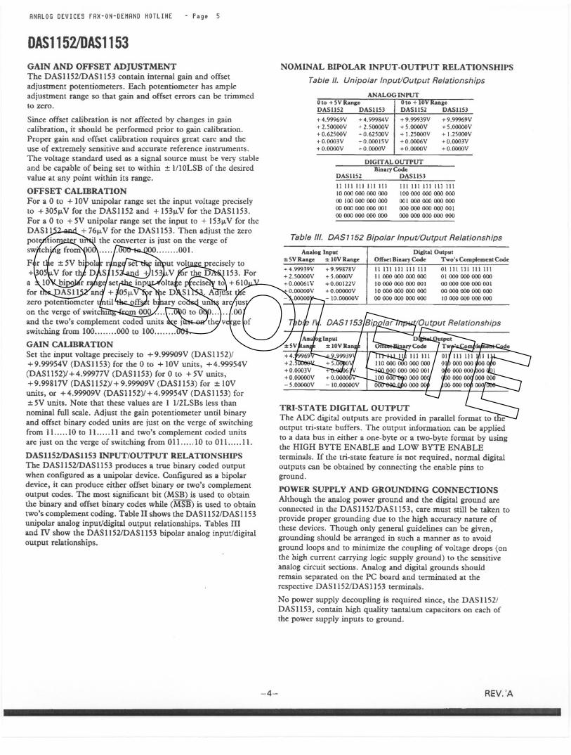
DAS1152/DAS1l53 INPUTIOUTPUT RELATIONSHIPSThe DAS1152/DAS1153 produces a true binary coded outputwhen configured as a unipolar device. Configured as a bipolardevice, it can produce either offset binary or two's complementoutput codes. The most significant bit (MSB) is used to obtainthe binary and offset binary codes while (MSB) is used to obtaintwo's complement coding. Table II shows the DAS 1I52/DAS 1153unipolar analog input/digital output relationships. Tables IIIand IV show the DAS1l52/DASllS3 bipolar analog input/digitaloutput relationships.
NOMINAL BIPOLAR INPUT .OUTPUT RELATIONSHIPS
Table II. Unipolar Input/Output Relationships
ANALOG INPUT010 +10DASHS2
+9,99939V+ ;,oooov+ !.25000V+0.0006V+O.OOOOV
Dto + SVRange:DASUS2 DASHS3
+4.99969V +4.99984V+2.50000V +2.50000Y+0.62500V +O.62500V+O.0003V +O.00015V+O.OOOOV +O.OOOOY
angeDASHS3
+9.9996!N+ 5.00000Y+ !.25000Y+O.0003V+O.OOOOV
QJGIT AL OUTPUTBinary Code
DASH53
111111111111111100 000 000 000 00000 1 000 000 000 000000 000 000 000 00 1000 000 000 000 000
DASllS2
1111111111111110 000 000 000 00000 100 000 000 00000 000 000 000 00 I00 000 000 000 000
Table /II. DAS1152 Bipolar Input/Ou~put Relationships
Analog Input:t:SVRange z 10VRange+ 4.99939V +9.99878V+ 2.50000Y + 5.0000Y+0.0006IY +0.OOI22Y+O.OOOOOV +O.OOOOOV- 5.00000Y - 10.00000Y
Digital OutputOffset Binary Code Two's Complemcot Code11111111111111 01111111111111II 000 000 000 000 01 000 000 000 00010000000 000 001 00 000 000 000 001I0 000 000 000 000 00 000 000 000 00000 000 000 000 000 I0 000 000 000 000
Table IV. DAS1153 Bipolar Input/Output Relationships
AIIaloe Input
: SVRange :!:10VRange
+4.99969V +9.99939V+2.50000V +5.0000Y+O.0003V + 0.0006IV+O.OOOOOV +O.OOOOOY- 5.00000V - IO.OOOOOV
Digital OutputOllSetBlnaryCode Two'. Complement Code
III III 111 111 111 011 III 111 III III110 000 000 000 000 010 000 000 000 000100 000 000 000 00I 000 000 000 000 001100 000 000 000 000 000 000 000 000 000000 000 000 000 000 I00 000 000 000 000
TRI-STATE DIGITAL OUTPUTThe ADC digital outputs are provided in parallel format to theoutput tri-state buffers. The oUtpUt information can be appliedto a data bus in either a one-byte or a two-byte format by usingthe HIGH BYTE ENABLE and LOW BYTE ENABLEterminals. If the tri-state feature is not required, normal digitaloutputs can be obtained by connecting the enable pins toground.
POWER SUPPLY AND GROUNDING CONNECTIONSAlthough the analog power ground and the digital ground areconnected in the DAS 1152/DASI 153, care must still be taken toprovide proper grounding due to the high accuracy nature ofthese devices. Though only general guidelines can be given,grounding should be arranged in such a manner as to avoidground loops and to minimize the coupling of voltage drops (onthe high current carrying logic supply ground) to the sensitiveanalog circuit sections. Analog and digital groW1dsshouldremain separated on the PC board and terminated at therespective DASI152/DAS 1153 terminals.
No power supply decoupling is required since, the DAS1152/DAS1l53, contain high quality tantalum capacitors on each ofthe power supply inputs to ground.
-4- REV. 'A
- -~
OBSOLETE