Embed Size (px)
Citation preview
TLV0834C, TLV0834I, TLV0838C, TLV0838I3-VOLT 8-BIT ANALOG-TO-DIGITAL CONVERTERS
WITH SERIAL CONTROLSLAS147B – SEPTEMBER 1996 – REVISED OCTOBER 2000
1POST OFFICE BOX 655303 • DALLAS, TEXAS 75265
8-Bit Resolution
2.7-V to 3.6-V VCC Easy Microprocessor Interface or
Stand-Alone Operation
Operates Ratiometrically or With V CCReference
4- or 8-Channel Multiplexer Options WithAddress Logic
Input Range 0 V to V CC With V CC Reference
Remote Operation With Serial Data Link
Inputs and Outputs Are Compatible WithTTL and MOS
Conversion Time of 32 µs atf(CLK) = 250 kHz
Functionally Equivalent to the ADC0834and ADC0838 at 3-V Supply Without theInternal Zener Regulator Network
Total Unadjusted Error . . . ±1 LSB
description
These devices are 8-bit successive-approximation analog-to-digital converters, each with an input-configurablemultichannel multiplexer and serial input/output. The serial input/output is configured to interface with standardshift registers or microprocessors. Detailed information on interfacing with most popular microprocessors isreadily available from the factory.
The TLV0834 (4-channel) and TLV0838 (8-channel) multiplexer is software-configured for single-ended ordifferential inputs as well as pseudodifferential input assignments. The differential analog voltage input allowsfor common-mode rejection or offset of the analog zero input voltage value. In addition, the voltage referenceinput can be adjusted to allow encoding of any smaller analog voltage span to the full 8 bits of resolution.
The TLV0834C and TLV0838C are characterized for operation from 0°C to 70°C. The TLV0834I and TLV0838Iare characterized for operation from –40°C to 85°C.
1
2
3
4
5
6
7
14
13
12
11
10
9
8
NCCS
CH0CH1CH2CH3
DGTL GND
VCCDICLKSARSDOREFANLG GND
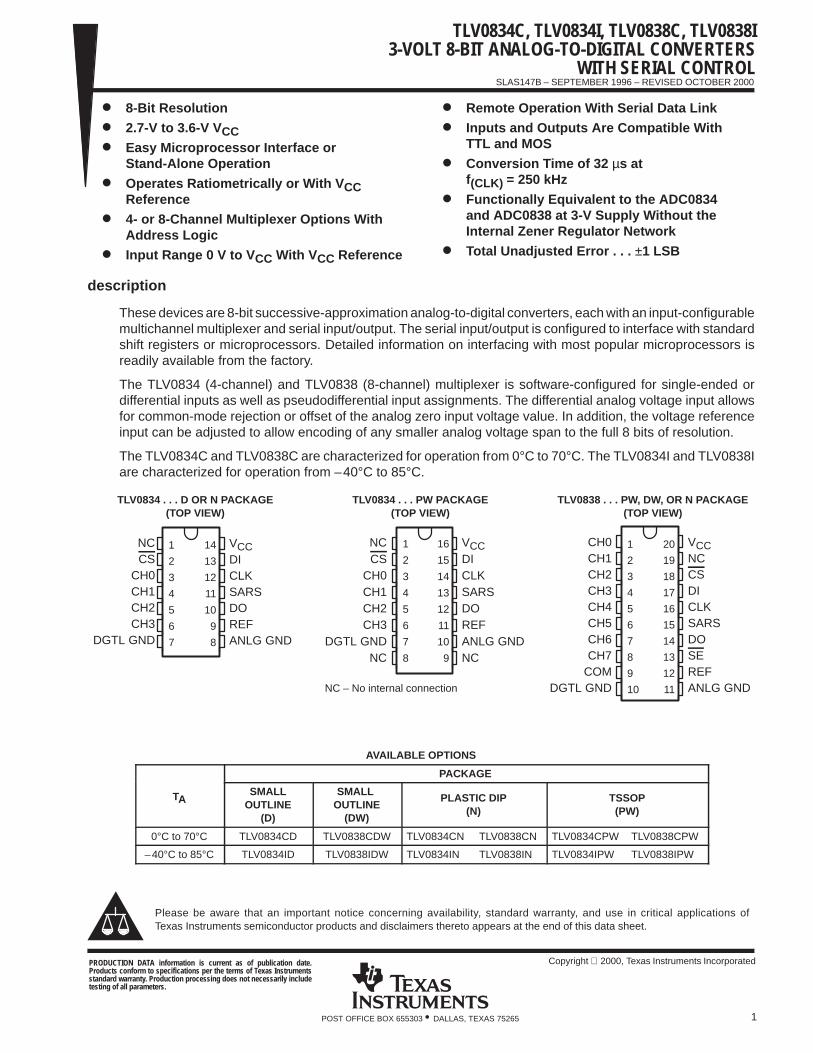
TLV0834 . . . D OR N PACKAGE(TOP VIEW)
1
2
3
4
5
6
7
8
16
15
14
13
12
11
10
9
NCCS
CH0CH1CH2CH3
DGTL GNDNC
VCCDICLKSARSDOREFANLG GNDNC
NC – No internal connection
TLV0834 . . . PW PACKAGE(TOP VIEW)
1
2
3
4
5
6
7
8
9
10
20
19
18
17
16
15
14
13
12
11
CH0CH1CH2CH3CH4CH5CH6CH7
COMDGTL GND
VCCNCCSDICLKSARSDOSEREFANLG GND
TLV0838 . . . PW, DW, OR N PACKAGE(TOP VIEW)
AVAILABLE OPTIONS
PACKAGE
TASMALL
OUTLINE(D)
SMALL OUTLINE
(DW)
PLASTIC DIP(N)
TSSOP(PW)
0°C to 70°C TLV0834CD TLV0838CDW TLV0834CN TLV0838CN TLV0834CPW TLV0838CPW
–40°C to 85°C TLV0834ID TLV0838IDW TLV0834IN TLV0838IN TLV0834IPW TLV0838IPW
Please be aware that an important notice concerning availability, standard warranty, and use in critical applications ofTexas Instruments semiconductor products and disclaimers thereto appears at the end of this data sheet.
PRODUCTION DATA information is current as of publication date.Products conform to specifications per the terms of Texas Instrumentsstandard warranty. Production processing does not necessarily includetesting of all parameters.
Copyright 2000, Texas Instruments Incorporated
TLV0834C, TLV0834I, TLV0838C, TLV0838I3-VO
LT 8-BIT ANALOG
-TO-DIG
ITAL CONVERTERS
WITH SERIAL CO
NTROL
SLA
S147B
– SE
PT
EM
BE
R 1996 – R
EV
ISE
D O
CT
OB
ER
2000
2P
OS
T O
FF
ICE
BO
X 655303 •
DA
LLAS
, TE
XA
S 75265
CS
SEOnly
5-Bit Shift Register
ODD\SELECT0
EN
MUXAnalog
STARTSGL\SELECT1
CircuitsTo Internal
(see Note A)DI
CLK
CS
RD
CLK
TLC0838
TLC0838
TLC0834
CH7
CH5CH6
COM
CH4CH3CH2CH1CH0
Comparator
SARS
CS
R
Start
S
CLK
CLK
DelayTime
SR
CS
DO
CSCS
D
CLKR
EOC
RegisterShift9-Bit
RCLK
FirstLSB
Bit 1
Bits 0–7
FirstMSB
ShotOne
Latchand
LogicSAR
R
CS
Bits 0–7
REF
Decoderand
Ladder
EN
Flip-Flop
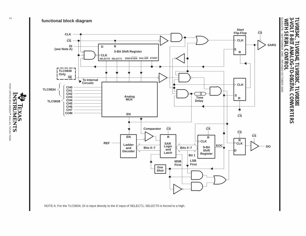
functional block diagram
NOTE A: For the TLC0834, DI is input directly to the D input of SELECT1; SELECT0 is forced to a high.
EVEN DIF
TLV0834C, TLV0834I, TLV0838C, TLV0838I3-VOLT 8-BIT ANALOG-TO-DIGITAL CONVERTERS
WITH SERIAL CONTROLSLAS147B – SEPTEMBER 1996 – REVISED OCTOBER 2000
3POST OFFICE BOX 655303 • DALLAS, TEXAS 75265
functional description
The TLV0834 and TLV0838 use a sample-data-comparator structure that converts differential analog inputs bya successive-approximation routine. Operation of both devices is similar with the exception of SE, an analogcommon input, and multiplexer addressing. The input voltage to be converted is applied to a channel terminaland is compared to ground (single ended), to an adjacent input (differential), or to a common terminal (pseudodifferential) that can be an arbitrary voltage. The input terminals are assigned a positive (+) or negative (–)polarity. When the signal input applied to the assigned positive terminal is less than the signal on the negativeterminal, the converter output is all zeros.
Channel selection and input configuration are under software control using a serial-data link from the controllingprocessor. A serial-communication format allows more functions to be included in a converter package with noincrease in size. In addition, it eliminates the transmission of low-level analog signals by locating the converterat the analog sensor and communicating serially with the controlling processor. This process returns noise-freedigital data to the processor.
A particular input configuration is assigned during the multiplexer-addressing sequence. The multiplexeraddress shifts into the converter through the data input (DI) line. The multiplexer address selects the analoginputs to be enabled and determines whether the input is single ended or differential. When the input isdifferential, the polarity of the channel input is assigned. Differential inputs are assigned to adjacent channelpairs . For example, channel 0 and channel 1 may be selected as a differential pair. These channels cannot actdifferentially with any other channel. In addition to selecting the differential mode, the polarity may also beselected. Either channel of the channel pair may be designated as the negative or positive input.
The common input on the TLV0838 can be used for a pseudodifferential input. In this mode, the voltage on thecommon input is considered to be the negative differential input for all channel inputs. This voltage can be anyreference potential common to all channel inputs. Each channel input can then be selected as the positivedifferential input. This feature is useful when all analog circuits are biased to a potential other than ground.
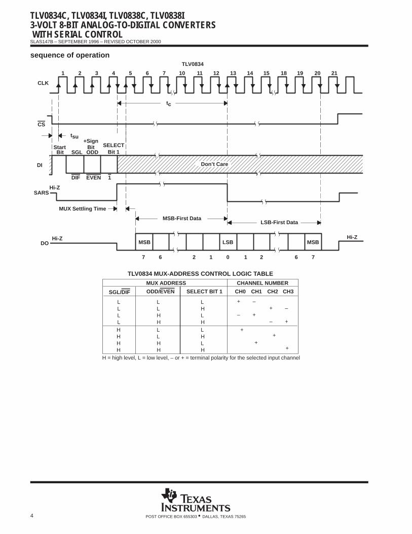
A conversion is initiated by setting CS low, which enables all logic circuits. CS must be held low for the completeconversion process. A clock input is then received from the processor. On each low-to-high transition of theclock input, the data on DI is clocked into the multiplexer-address shift register. The first logic high on the inputis the start bit. A 3- to 4-bit assignment word follows the start bit. On each successive low-to-high transition ofthe clock input, the start bit and assignment word are shifted through the shift register. When the start bit isshifted into the start location of the multiplexer register, the input channel is selected and conversion starts. TheSAR status output (SARS) goes high to indicate that a conversion is in progress, and DI to the multiplexer shiftregister is disabled for the duration of the conversion.
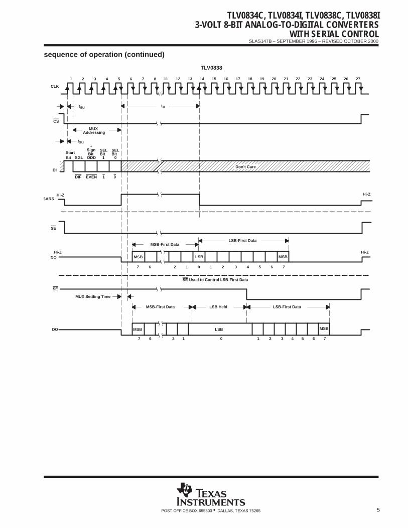
An interval of one clock period is automatically inserted to allow the selected multiplexed channel to settle. DOcomes out of the high-impedance state and provides a leading low for one clock period of multiplexer settlingtime. The SAR comparator compares successive outputs from the resistive ladder with the incoming analogsignal. The comparator output indicates whether the analog input is greater than or less than the resistive-ladderoutput. As the conversion proceeds, conversion data is simultaneously output from DO, with the most significantbit (MSB) first. After eight clock periods, the conversion is complete and SARS goes low.
The TLV0834 outputs the least-significant-bit (LSB) first data after the MSB-first data stream. When SE is heldhigh on the TLV0838, the value of the LSB remains on the data line. When SE is forced low, the data is thenclocked out as LSB-first data. (To output LSB first, SE must first go low, then the data stored in the 9-bit shiftregister outputs LSB first.) When CS goes high, all internal registers are cleared. At this time, the output circuitsgo to the high-impedance state. If another conversion is desired, CS must make a high-to-low transition followedby address information.
DI and DO can be tied together and controlled by a bidirectional processor I/O bit received on a single wire. Thisis possible because DI is only examined during the multiplexer-addressing interval and DO is still in thehigh-impedance state.
TLV0834C, TLV0834I, TLV0838C, TLV0838I3-VOLT 8-BIT ANALOG-TO-DIGITAL CONVERTERS WITH SERIAL CONTROL
SLAS147B – SEPTEMBER 1996 – REVISED OCTOBER 2000
4 POST OFFICE BOX 655303 • DALLAS, TEXAS 75265
sequence of operation
SELECTBit 1
157
1
Bit
tsu
Hi-ZSARS
Don’t Care
1 76201267
MSBLSB
LSB-First DataMSB-First Data
EVENDIF
ODD
+Sign
SGLBitStart
MSB
MUX Settling Time
DI
DO
CS
CLK
212019181413121 2 3 4 5 6 10 11
tc
Hi-Z Hi-Z
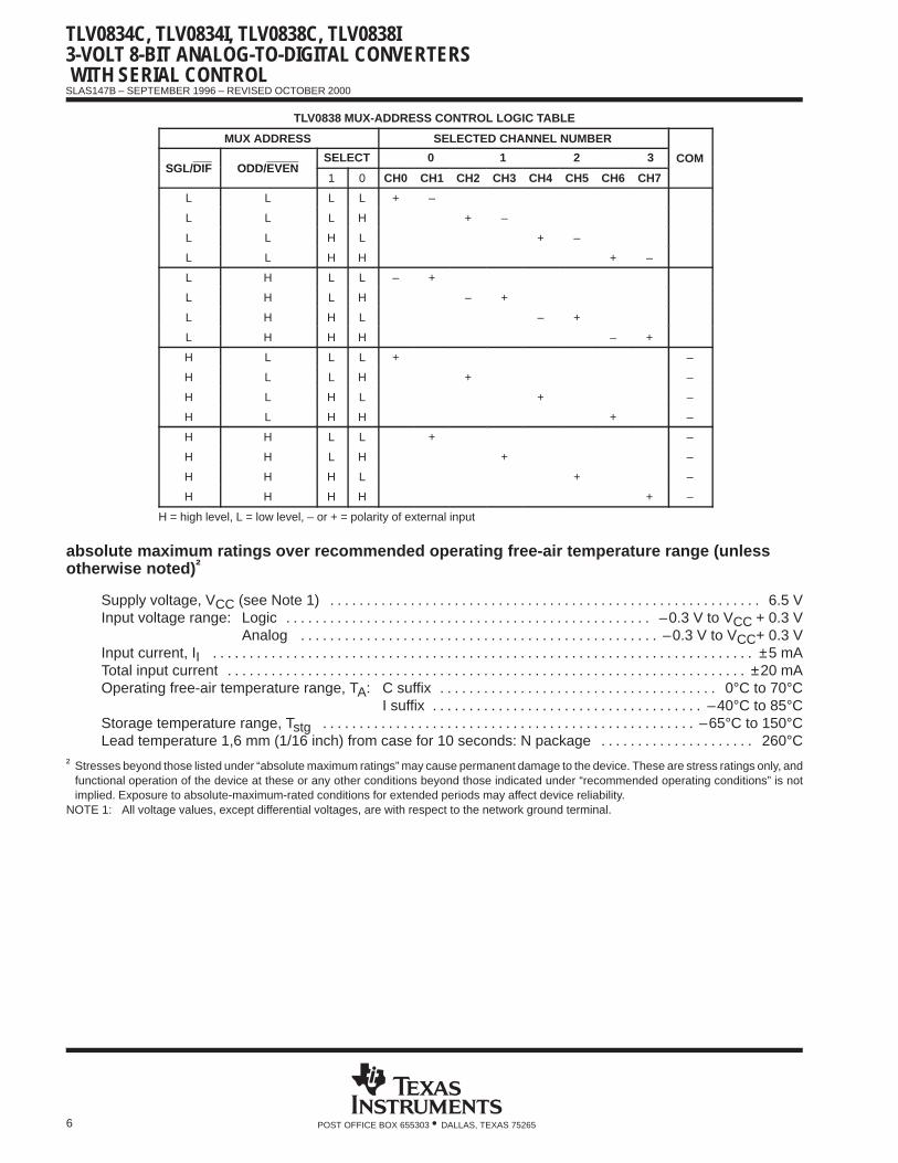
TLV0834 MUX-ADDRESS CONTROL LOGIC TABLE
MUX ADDRESS CHANNEL NUMBER
SGL/DIF ODD/EVEN
LLHH
LHLH
CH0 CH1SELECT BIT 1
LLHH
LHLH
LLLLHHHH
CH2 CH3
+
–
–
++
–
–
+
+
++
+
TLV0834
H = high level, L = low level, – or + = terminal polarity for the selected input channel
TLV0834C, TLV0834I, TLV0838C, TLV0838I3-VOLT 8-BIT ANALOG-TO-DIGITAL CONVERTERS
WITH SERIAL CONTROLSLAS147B – SEPTEMBER 1996 – REVISED OCTOBER 2000
5POST OFFICE BOX 655303 • DALLAS, TEXAS 75265
sequence of operation (continued)
1SGL ODDBit
SE
LSB
MSBLSB
765432101267
MSB
MUX Settling Time
DO
LSB Held LSB-First DataMSB-First Data
SE Used to Control LSB-First Data
Hi-Z
Hi-Z
tc
Don’t Care
765432101267
MSB
LSB-First DataMSB-First Data
MSBHi-Z
DO
SE
SARSHi-Z
SELSEL+
Bit0
01EVENDIF
DI
BitStart
CS
AddressingMUX
tsu
tsu
CLK
272625242322212019181716151413121187654321
TLV0838
SignBit
TLV0834C, TLV0834I, TLV0838C, TLV0838I3-VOLT 8-BIT ANALOG-TO-DIGITAL CONVERTERS WITH SERIAL CONTROL
SLAS147B – SEPTEMBER 1996 – REVISED OCTOBER 2000
6 POST OFFICE BOX 655303 • DALLAS, TEXAS 75265
TLV0838 MUX-ADDRESS CONTROL LOGIC TABLE
MUX ADDRESS SELECTED CHANNEL NUMBER
SGL/DIF ODD/EVENSELECT 0 1 2 3 COM
SGL/DIF ODD/EVEN1 0 CH0 CH1 CH2 CH3 CH4 CH5 CH6 CH7
L L L L + –
L L L H + –
L L H L + –
L L H H + –
L H L L – +
L H L H – +
L H H L – +
L H H H – +
H L L L + –
H L L H + –
H L H L + –
H L H H + –
H H L L + –
H H L H + –
H H H L + –
H H H H + –
H = high level, L = low level, – or + = polarity of external input
absolute maximum ratings over recommended operating free-air temperature range (unlessotherwise noted) †
Supply voltage, VCC (see Note 1) 6.5 V. . . . . . . . . . . . . . . . . . . . . . . . . . . . . . . . . . . . . . . . . . . . . . . . . . . . . . . . . . . Input voltage range: Logic –0.3 V to VCC + 0.3 V. . . . . . . . . . . . . . . . . . . . . . . . . . . . . . . . . . . . . . . . . . . . . . . . . .
Analog –0.3 V to VCC+ 0.3 V. . . . . . . . . . . . . . . . . . . . . . . . . . . . . . . . . . . . . . . . . . . . . . . . . Input current, II ±5 mA. . . . . . . . . . . . . . . . . . . . . . . . . . . . . . . . . . . . . . . . . . . . . . . . . . . . . . . . . . . . . . . . . . . . . . . . . . Total input current ±20 mA. . . . . . . . . . . . . . . . . . . . . . . . . . . . . . . . . . . . . . . . . . . . . . . . . . . . . . . . . . . . . . . . . . . . . . . Operating free-air temperature range, TA: C suffix 0°C to 70°C. . . . . . . . . . . . . . . . . . . . . . . . . . . . . . . . . . . . . .
I suffix –40°C to 85°C. . . . . . . . . . . . . . . . . . . . . . . . . . . . . . . . . . . . . Storage temperature range, Tstg –65°C to 150°C. . . . . . . . . . . . . . . . . . . . . . . . . . . . . . . . . . . . . . . . . . . . . . . . . . . Lead temperature 1,6 mm (1/16 inch) from case for 10 seconds: N package 260°C. . . . . . . . . . . . . . . . . . . . .
† Stresses beyond those listed under “absolute maximum ratings” may cause permanent damage to the device. These are stress ratings only, andfunctional operation of the device at these or any other conditions beyond those indicated under “recommended operating conditions” is notimplied. Exposure to absolute-maximum-rated conditions for extended periods may affect device reliability.
NOTE 1: All voltage values, except differential voltages, are with respect to the network ground terminal.
TLV0834C, TLV0834I, TLV0838C, TLV0838I3-VOLT 8-BIT ANALOG-TO-DIGITAL CONVERTERS
WITH SERIAL CONTROLSLAS147B – SEPTEMBER 1996 – REVISED OCTOBER 2000
7POST OFFICE BOX 655303 • DALLAS, TEXAS 75265
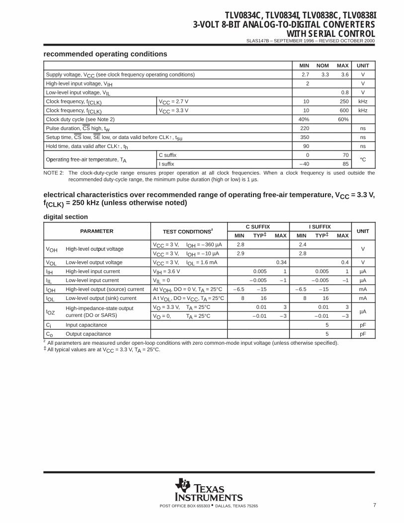
recommended operating conditions
MIN NOM MAX UNIT
Supply voltage, VCC (see clock frequency operating conditions) 2.7 3.3 3.6 V
High-level input voltage, VIH 2 V
Low-level input voltage, VIL 0.8 V
Clock frequency, f(CLK) VCC = 2.7 V 10 250 kHz
Clock frequency, f(CLK) VCC = 3.3 V 10 600 kHz
Clock duty cycle (see Note 2) 40% 60%
Pulse duration, CS high, tw 220 ns
Setup time, CS low, SE low, or data valid before CLK↑ , tsu 350 ns
Hold time, data valid after CLK↑ , th 90 ns
Operating free air temperature TAC suffix 0 70
°COperating free-air temperature, TAI suffix –40 85
°C
NOTE 2: The clock-duty-cycle range ensures proper operation at all clock frequencies. When a clock frequency is used outside therecommended duty-cycle range, the minimum pulse duration (high or low) is 1 µs.
electrical characteristics over recommended range of operating free-air temperature, V CC = 3.3 V,f(CLK) = 250 kHz (unless otherwise noted)
digital section
PARAMETER TEST CONDITIONS†C SUFFIX I SUFFIX
UNITPARAMETER TEST CONDITIONS†MIN TYP‡ MAX MIN TYP‡ MAX
UNIT
VOH High level output voltageVCC = 3 V, IOH = –360 µA 2.8 2.4
VVOH High-level output voltageVCC = 3 V, IOH = –10 µA 2.9 2.8
V
VOL Low-level output voltage VCC = 3 V, IOL = 1.6 mA 0.34 0.4 V
IIH High-level input current VIH = 3.6 V 0.005 1 0.005 1 µA
IIL Low-level input current VIL = 0 –0.005 –1 –0.005 –1 µA
IOH High-level output (source) current At VOH, DO = 0 V, TA = 25°C –6.5 –15 –6.5 –15 mA
IOL Low-level output (sink) current A t VOL, DO = VCC, TA = 25°C 8 16 8 16 mA
IOZHigh-impedance-state output VO = 3.3 V, TA = 25°C 0.01 3 0.01 3
µAIOZg
current (DO or SARS) VO = 0, TA = 25°C –0.01 –3 –0.01 –3µA
Ci Input capacitance 5 pF
Co Output capacitance 5 pF
† All parameters are measured under open-loop conditions with zero common-mode input voltage (unless otherwise specified).‡ All typical values are at VCC = 3.3 V, TA = 25°C.
TLV0834C, TLV0834I, TLV0838C, TLV0838I3-VOLT 8-BIT ANALOG-TO-DIGITAL CONVERTERS WITH SERIAL CONTROL
SLAS147B – SEPTEMBER 1996 – REVISED OCTOBER 2000
8 POST OFFICE BOX 655303 • DALLAS, TEXAS 75265
electrical characteristics over recommended range of operating free-air temperature, V CC = 3.3 V,f(CLK) = 250 kHz (unless otherwise noted) (continued)
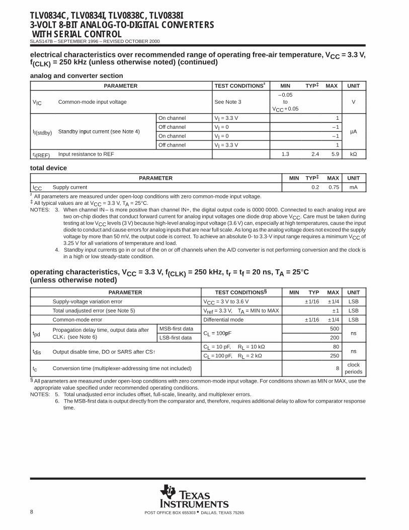
analog and converter sectionPARAMETER TEST CONDITIONS† MIN TYP‡ MAX UNIT
–0.05VIC Common-mode input voltage See Note 3 to VIC g
VCC+0.05
On channel VI = 3.3 V 1
II( tdb ) Standby input current (see Note 4)Off channel VI = 0 –1
µAII(stdby) Standby input current (see Note 4)On channel VI = 0 –1
µA
Off channel VI = 3.3 V 1
ri(REF) Input resistance to REF 1.3 2.4 5.9 kΩ
total devicePARAMETER MIN TYP‡ MAX UNIT
ICC Supply current 0.2 0.75 mA
† All parameters are measured under open-loop conditions with zero common-mode input voltage.‡ All typical values are at VCC = 3.3 V, TA = 25°C.NOTES: 3. When channel IN– is more positive than channel IN+, the digital output code is 0000 0000. Connected to each analog input are
two on-chip diodes that conduct forward current for analog input voltages one diode drop above VCC. Care must be taken duringtesting at low VCC levels (3 V) because high-level analog input voltage (3.6 V) can, especially at high temperatures, cause the inputdiode to conduct and cause errors for analog inputs that are near full scale. As long as the analog voltage does not exceed the supplyvoltage by more than 50 mV, the output code is correct. To achieve an absolute 0- to 3.3-V input range requires a minimum VCC of3.25 V for all variations of temperature and load.
4. Standby input currents go in or out of the on or off channels when the A/D converter is not performing conversion and the clock isin a high or low steady-state condition.
operating characteristics, V CC = 3.3 V, f(CLK) = 250 kHz, t r = tf = 20 ns, TA = 25°C (unless otherwise noted)
PARAMETER TEST CONDITIONS§ MIN TYP MAX UNIT
Supply-voltage variation error VCC = 3 V to 3.6 V ±1/16 ±1/4 LSB
Total unadjusted error (see Note 5) Vref = 3.3 V, TA = MIN to MAX ±1 LSB
Common-mode error Differential mode ±1/16 ±1/4 LSB
t dPropagation delay time, output data after MSB-first data
CL = 100pF500
nstpdg y ,
CLK↓ (see Note 6) LSB-first dataCL = 100pF
200ns
tdi Output disable time DO or SARS after CS↑CL = 10 pF, RL = 10 kΩ 80
nstdis Output disable time, DO or SARS after CS↑CL = 100 pF, RL = 2 kΩ 250
ns
tc Conversion time (multiplexer-addressing time not included) 8clock
periods
§ All parameters are measured under open-loop conditions with zero common-mode input voltage. For conditions shown as MIN or MAX, use theappropriate value specified under recommended operating conditions.
NOTES: 5. Total unadjusted error includes offset, full-scale, linearity, and multiplexer errors.6. The MSB-first data is output directly from the comparator and, therefore, requires additional delay to allow for comparator response
time.
TLV0834C, TLV0834I, TLV0838C, TLV0838I3-VOLT 8-BIT ANALOG-TO-DIGITAL CONVERTERS
WITH SERIAL CONTROLSLAS147B – SEPTEMBER 1996 – REVISED OCTOBER 2000
9POST OFFICE BOX 655303 • DALLAS, TEXAS 75265
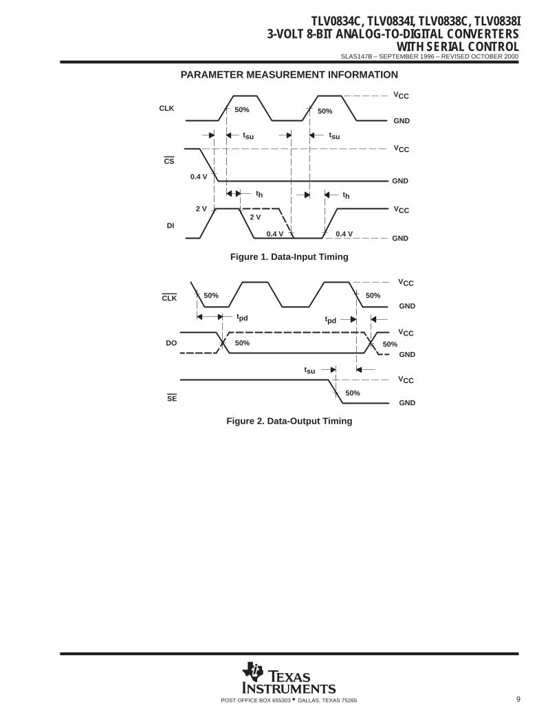
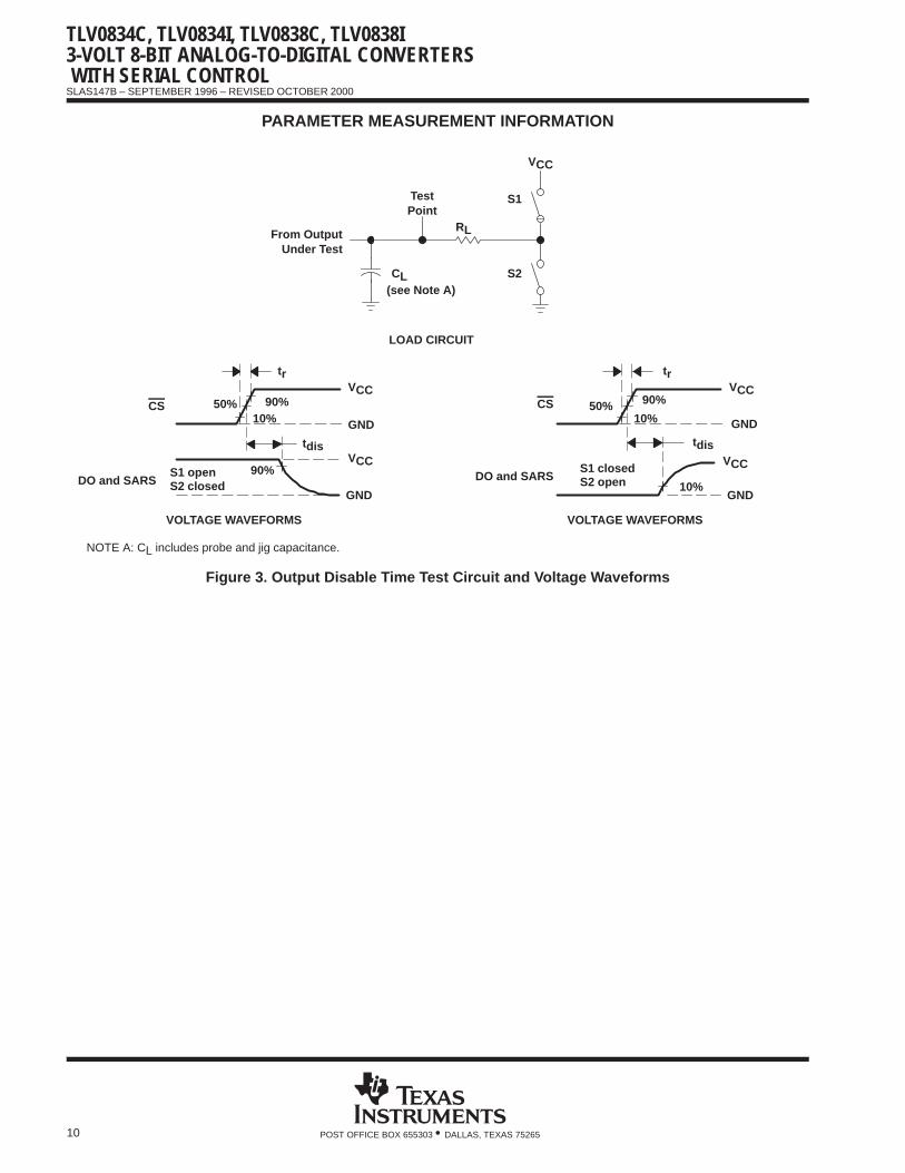
PARAMETER MEASUREMENT INFORMATION
50%
tsu
th th
tsu
50%
VCC
GND
GND
GND0.4 V0.4 V
2 V2 V
DI
0.4 V
CS
CLK
VCC
VCC
Figure 1. Data-Input Timing
tsu
tpdtpd
SE
CLK
DO
50%
50%
50%
50%
50%
GND
GND
GND
VCC
VCC
VCC
Figure 2. Data-Output Timing
TLV0834C, TLV0834I, TLV0838C, TLV0838I3-VOLT 8-BIT ANALOG-TO-DIGITAL CONVERTERS WITH SERIAL CONTROL
SLAS147B – SEPTEMBER 1996 – REVISED OCTOBER 2000
10 POST OFFICE BOX 655303 • DALLAS, TEXAS 75265
PARAMETER MEASUREMENT INFORMATION
VOLTAGE WAVEFORMS
S2 openS1 closed
10%
10%
90%
tr
VOLTAGE WAVEFORMS
S2 closedS1 open
DO and SARS
tr
S1
S2
LOAD CIRCUIT
(see Note A)CL
From OutputUnder Test
TestPoint
CSCS
tdis
90%
10%90%50% 50%
VCC
GND
GND
GND
GND
VCC
VCC
VCC
VCC
RL
DO and SARS
tdis
NOTE A: CL includes probe and jig capacitance.
Figure 3. Output Disable Time Test Circuit and Voltage Waveforms
TLV0834C, TLV0834I, TLV0838C, TLV0838I3-VOLT 8-BIT ANALOG-TO-DIGITAL CONVERTERS
WITH SERIAL CONTROLSLAS147B – SEPTEMBER 1996 – REVISED OCTOBER 2000
11POST OFFICE BOX 655303 • DALLAS, TEXAS 75265
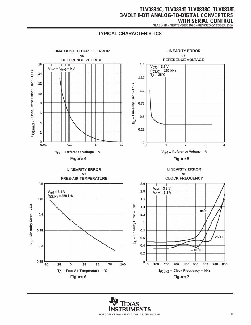
TYPICAL CHARACTERISTICS
Vref – Reference Voltage – V
1010.10.01
VI(+) = VI(–) = 0 V
0
2
4
6
8
10
12
14
16
UNADJUSTED OFFSET ERRORvs
REFERENCE VOLTAGE
EO
(una
dj)
– U
nadj
uste
d O
ffset
Err
or –
LS
B
Figure 4 Figure 5
Vref – Reference Voltage – V
VCC = 3.3 Vf(CLK) = 250 kHzTA = 25°C
43210
0.25
0.5
0.75
1.0
1.25
0
1.5
LINEARITY ERRORvs
REFERENCE VOLTAGE
– Li
near
ity E
rror
– L
SB
EL
Figure 6
TA – Free-Air Temperature – °C
Vref = 3.3 Vf(CLK) = 250 kHz
1007550250–25
0.5
0.45
0.4
0.35
0.3
–500.25
LINEARITY ERRORvs
FREE-AIR TEMPERATURE
– Li
near
ity E
rror
– L
SB
EL
Figure 7
f(CLK) – Clock Frequency – kHz
LINEARITY ERRORvs
CLOCK FREQUENCY
– Li
near
ity E
rror
– L
SB
EL
600500400300200100
2.0
1.8
1.2
1
0.8
0.2
00
85°C
25°C
–40°C
Vref = 3.3 VVCC = 3.3 V
1.6
1.4
0.6
0.4
700 800
TLV0834C, TLV0834I, TLV0838C, TLV0838I3-VOLT 8-BIT ANALOG-TO-DIGITAL CONVERTERS WITH SERIAL CONTROL
SLAS147B – SEPTEMBER 1996 – REVISED OCTOBER 2000
12 POST OFFICE BOX 655303 • DALLAS, TEXAS 75265
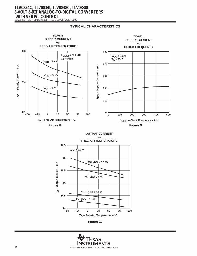
TYPICAL CHARACTERISTICS
Figure 8
TA – Free-Air Temperature – °C
f(CLK) = 250 kHzCS = High
VCC = 3.6 V
VCC = 3 V
1007550250–25
0.3
0.2
–500.1
– S
uppl
y C
urre
nt –
mA
TLV0831SUPPLY CURRENT
vsFREE-AIR TEMPERATURE
CC
I
VCC = 3.3 V
Figure 9
f(CLK) – Clock Frequency – kHz
TLV0831SUPPLY CURRENT
vsCLOCK FREQUENCY
– S
uppl
y C
urre
nt –
mA
CC
I
VCC = 3.3 VTA = 25°C
50040030020010000
0.1
0.2
0.3
0.4
0.5
TA – Free-Air Temperature – °C
VCC = 3.3 V
IOL (DO = 0.4 V)
16
16.5
15.5
15
14.5
1007550250–25–5014
– O
utpu
t Cur
rent
– m
A
OUTPUT CURRENTvs
FREE-AIR TEMPERATURE
I O
IOL (DO = 3.3 V)
– IOH (DO = 0 V)
– IOH (DO = 2.4 V)
Figure 10
TLV0834C, TLV0834I, TLV0838C, TLV0838I3-VOLT 8-BIT ANALOG-TO-DIGITAL CONVERTERS
WITH SERIAL CONTROLSLAS147B – SEPTEMBER 1996 – REVISED OCTOBER 2000
13POST OFFICE BOX 655303 • DALLAS, TEXAS 75265
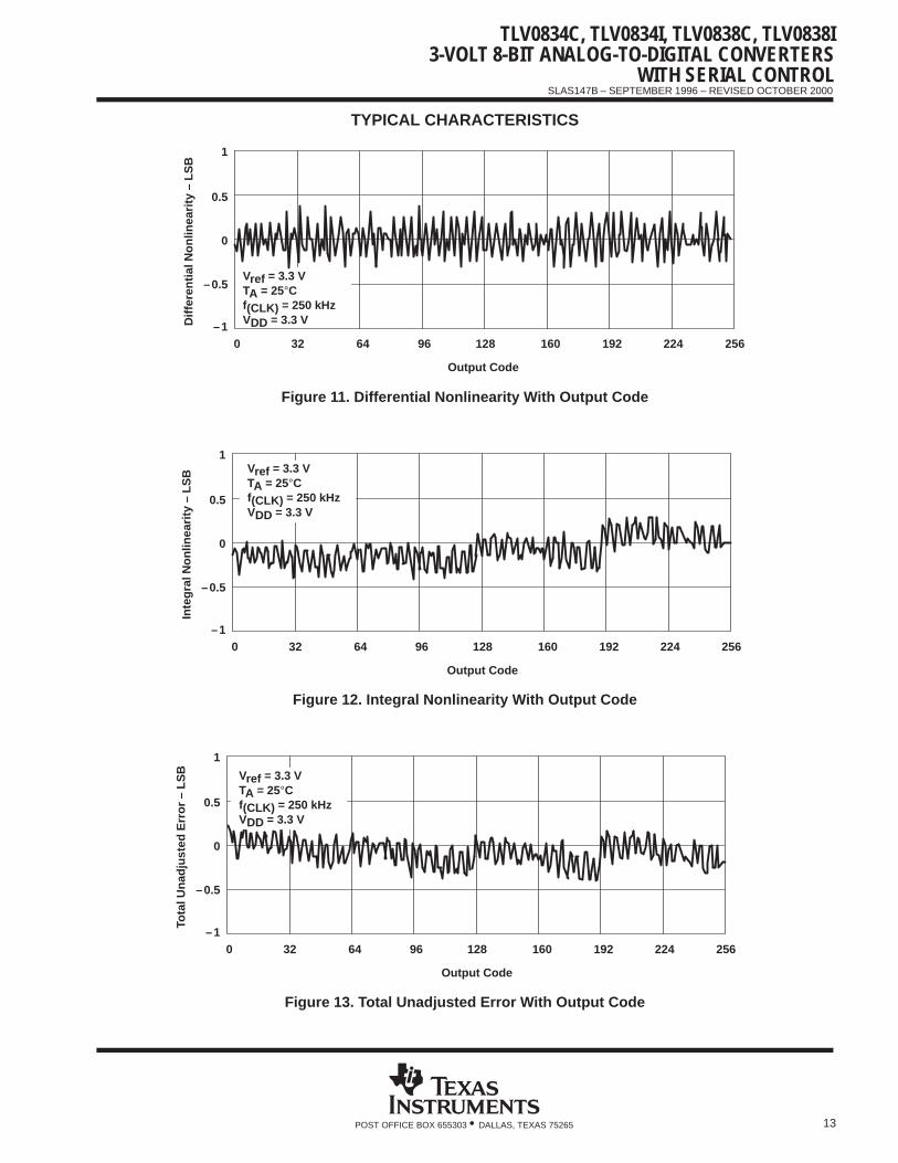
TYPICAL CHARACTERISTICS
Diff
eren
tial N
onlin
earit
y –
LSB
–1
Output Code
1
0.5
0
–0.5
0 32 64 96 128 160 192 224 256
Vref = 3.3 VTA = 25°Cf(CLK) = 250 kHzVDD = 3.3 V
Figure 11. Differential Nonlinearity With Output Code
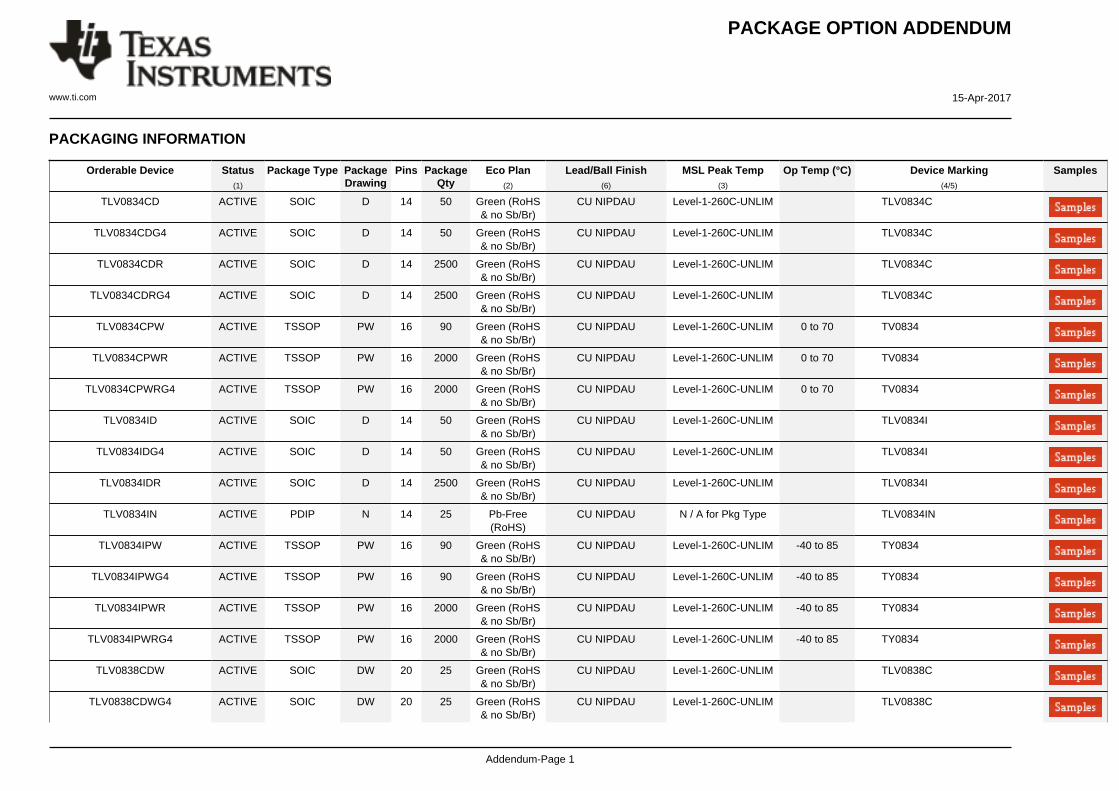
Inte
gral
Non
linea
rity
– LS
B
–1
Output Code
1
0.5
0
–0.5
0 32 64 96 128 160 192 224 256
Vref = 3.3 VTA = 25°Cf(CLK) = 250 kHzVDD = 3.3 V
Figure 12. Integral Nonlinearity With Output Code
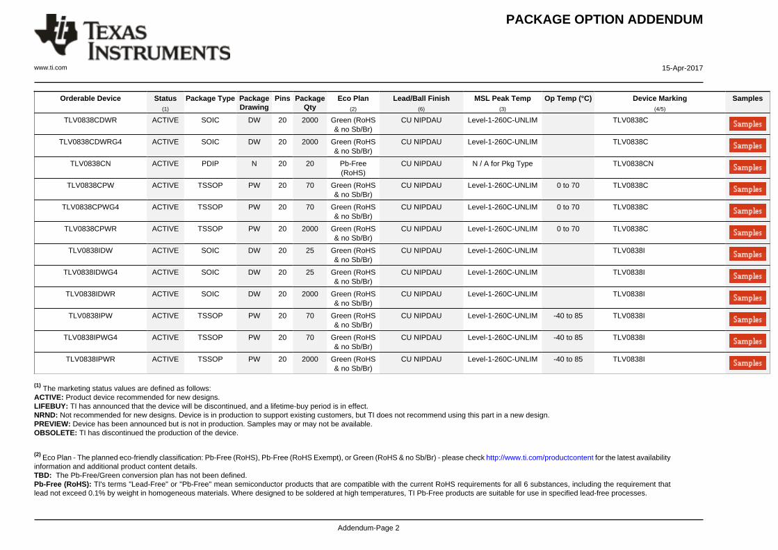
Tota
l Una
djus
ted
Err
or –
LS
B
–1
Output Code
1
0.5
0
–0.5
0 32 64 96 128 160 192 224 256
Vref = 3.3 VTA = 25°Cf(CLK) = 250 kHzVDD = 3.3 V
Figure 13. Total Unadjusted Error With Output Code
PACKAGE OPTION ADDENDUM
www.ti.com 15-Apr-2017
Addendum-Page 1
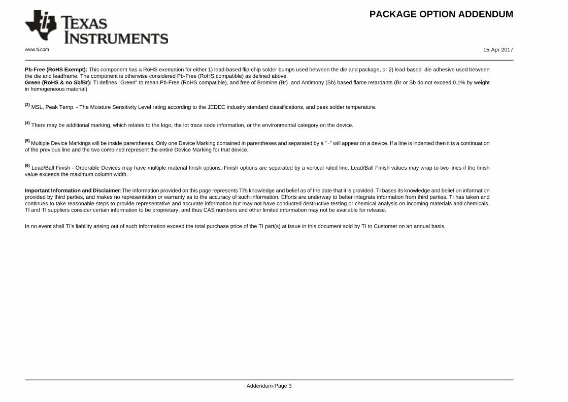
PACKAGING INFORMATION
Orderable Device Status(1)
Package Type PackageDrawing
Pins PackageQty
Eco Plan(2)
Lead/Ball Finish(6)
MSL Peak Temp(3)
Op Temp (°C) Device Marking(4/5)
Samples
TLV0834CD ACTIVE SOIC D 14 50 Green (RoHS& no Sb/Br)
CU NIPDAU Level-1-260C-UNLIM TLV0834C
TLV0834CDG4 ACTIVE SOIC D 14 50 Green (RoHS& no Sb/Br)
CU NIPDAU Level-1-260C-UNLIM TLV0834C
TLV0834CDR ACTIVE SOIC D 14 2500 Green (RoHS& no Sb/Br)
CU NIPDAU Level-1-260C-UNLIM TLV0834C
TLV0834CDRG4 ACTIVE SOIC D 14 2500 Green (RoHS& no Sb/Br)
CU NIPDAU Level-1-260C-UNLIM TLV0834C
TLV0834CPW ACTIVE TSSOP PW 16 90 Green (RoHS& no Sb/Br)
CU NIPDAU Level-1-260C-UNLIM 0 to 70 TV0834
TLV0834CPWR ACTIVE TSSOP PW 16 2000 Green (RoHS& no Sb/Br)
CU NIPDAU Level-1-260C-UNLIM 0 to 70 TV0834
TLV0834CPWRG4 ACTIVE TSSOP PW 16 2000 Green (RoHS& no Sb/Br)
CU NIPDAU Level-1-260C-UNLIM 0 to 70 TV0834
TLV0834ID ACTIVE SOIC D 14 50 Green (RoHS& no Sb/Br)
CU NIPDAU Level-1-260C-UNLIM TLV0834I
TLV0834IDG4 ACTIVE SOIC D 14 50 Green (RoHS& no Sb/Br)
CU NIPDAU Level-1-260C-UNLIM TLV0834I
TLV0834IDR ACTIVE SOIC D 14 2500 Green (RoHS& no Sb/Br)
CU NIPDAU Level-1-260C-UNLIM TLV0834I
TLV0834IN ACTIVE PDIP N 14 25 Pb-Free(RoHS)
CU NIPDAU N / A for Pkg Type TLV0834IN
TLV0834IPW ACTIVE TSSOP PW 16 90 Green (RoHS& no Sb/Br)
CU NIPDAU Level-1-260C-UNLIM -40 to 85 TY0834
TLV0834IPWG4 ACTIVE TSSOP PW 16 90 Green (RoHS& no Sb/Br)
CU NIPDAU Level-1-260C-UNLIM -40 to 85 TY0834
TLV0834IPWR ACTIVE TSSOP PW 16 2000 Green (RoHS& no Sb/Br)
CU NIPDAU Level-1-260C-UNLIM -40 to 85 TY0834
TLV0834IPWRG4 ACTIVE TSSOP PW 16 2000 Green (RoHS& no Sb/Br)
CU NIPDAU Level-1-260C-UNLIM -40 to 85 TY0834
TLV0838CDW ACTIVE SOIC DW 20 25 Green (RoHS& no Sb/Br)
CU NIPDAU Level-1-260C-UNLIM TLV0838C
TLV0838CDWG4 ACTIVE SOIC DW 20 25 Green (RoHS& no Sb/Br)
CU NIPDAU Level-1-260C-UNLIM TLV0838C
PACKAGE OPTION ADDENDUM
www.ti.com 15-Apr-2017
Addendum-Page 2
Orderable Device Status(1)
Package Type PackageDrawing
Pins PackageQty
Eco Plan(2)
Lead/Ball Finish(6)
MSL Peak Temp(3)
Op Temp (°C) Device Marking(4/5)
Samples
TLV0838CDWR ACTIVE SOIC DW 20 2000 Green (RoHS& no Sb/Br)
CU NIPDAU Level-1-260C-UNLIM TLV0838C
TLV0838CDWRG4 ACTIVE SOIC DW 20 2000 Green (RoHS& no Sb/Br)
CU NIPDAU Level-1-260C-UNLIM TLV0838C
TLV0838CN ACTIVE PDIP N 20 20 Pb-Free(RoHS)
CU NIPDAU N / A for Pkg Type TLV0838CN
TLV0838CPW ACTIVE TSSOP PW 20 70 Green (RoHS& no Sb/Br)
CU NIPDAU Level-1-260C-UNLIM 0 to 70 TLV0838C
TLV0838CPWG4 ACTIVE TSSOP PW 20 70 Green (RoHS& no Sb/Br)
CU NIPDAU Level-1-260C-UNLIM 0 to 70 TLV0838C
TLV0838CPWR ACTIVE TSSOP PW 20 2000 Green (RoHS& no Sb/Br)
CU NIPDAU Level-1-260C-UNLIM 0 to 70 TLV0838C
TLV0838IDW ACTIVE SOIC DW 20 25 Green (RoHS& no Sb/Br)
CU NIPDAU Level-1-260C-UNLIM TLV0838I
TLV0838IDWG4 ACTIVE SOIC DW 20 25 Green (RoHS& no Sb/Br)
CU NIPDAU Level-1-260C-UNLIM TLV0838I
TLV0838IDWR ACTIVE SOIC DW 20 2000 Green (RoHS& no Sb/Br)
CU NIPDAU Level-1-260C-UNLIM TLV0838I
TLV0838IPW ACTIVE TSSOP PW 20 70 Green (RoHS& no Sb/Br)
CU NIPDAU Level-1-260C-UNLIM -40 to 85 TLV0838I
TLV0838IPWG4 ACTIVE TSSOP PW 20 70 Green (RoHS& no Sb/Br)
CU NIPDAU Level-1-260C-UNLIM -40 to 85 TLV0838I
TLV0838IPWR ACTIVE TSSOP PW 20 2000 Green (RoHS& no Sb/Br)
CU NIPDAU Level-1-260C-UNLIM -40 to 85 TLV0838I
(1) The marketing status values are defined as follows:ACTIVE: Product device recommended for new designs.LIFEBUY: TI has announced that the device will be discontinued, and a lifetime-buy period is in effect.NRND: Not recommended for new designs. Device is in production to support existing customers, but TI does not recommend using this part in a new design.PREVIEW: Device has been announced but is not in production. Samples may or may not be available.OBSOLETE: TI has discontinued the production of the device.
(2) Eco Plan - The planned eco-friendly classification: Pb-Free (RoHS), Pb-Free (RoHS Exempt), or Green (RoHS & no Sb/Br) - please check http://www.ti.com/productcontent for the latest availabilityinformation and additional product content details.TBD: The Pb-Free/Green conversion plan has not been defined.Pb-Free (RoHS): TI's terms "Lead-Free" or "Pb-Free" mean semiconductor products that are compatible with the current RoHS requirements for all 6 substances, including the requirement thatlead not exceed 0.1% by weight in homogeneous materials. Where designed to be soldered at high temperatures, TI Pb-Free products are suitable for use in specified lead-free processes.
PACKAGE OPTION ADDENDUM
www.ti.com 15-Apr-2017
Addendum-Page 3
Pb-Free (RoHS Exempt): This component has a RoHS exemption for either 1) lead-based flip-chip solder bumps used between the die and package, or 2) lead-based die adhesive used betweenthe die and leadframe. The component is otherwise considered Pb-Free (RoHS compatible) as defined above.Green (RoHS & no Sb/Br): TI defines "Green" to mean Pb-Free (RoHS compatible), and free of Bromine (Br) and Antimony (Sb) based flame retardants (Br or Sb do not exceed 0.1% by weightin homogeneous material)
(3) MSL, Peak Temp. - The Moisture Sensitivity Level rating according to the JEDEC industry standard classifications, and peak solder temperature.
(4) There may be additional marking, which relates to the logo, the lot trace code information, or the environmental category on the device.
(5) Multiple Device Markings will be inside parentheses. Only one Device Marking contained in parentheses and separated by a "~" will appear on a device. If a line is indented then it is a continuationof the previous line and the two combined represent the entire Device Marking for that device.
(6) Lead/Ball Finish - Orderable Devices may have multiple material finish options. Finish options are separated by a vertical ruled line. Lead/Ball Finish values may wrap to two lines if the finishvalue exceeds the maximum column width.
Important Information and Disclaimer:The information provided on this page represents TI's knowledge and belief as of the date that it is provided. TI bases its knowledge and belief on informationprovided by third parties, and makes no representation or warranty as to the accuracy of such information. Efforts are underway to better integrate information from third parties. TI has taken andcontinues to take reasonable steps to provide representative and accurate information but may not have conducted destructive testing or chemical analysis on incoming materials and chemicals.TI and TI suppliers consider certain information to be proprietary, and thus CAS numbers and other limited information may not be available for release.
In no event shall TI's liability arising out of such information exceed the total purchase price of the TI part(s) at issue in this document sold by TI to Customer on an annual basis.
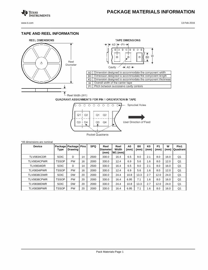
TAPE AND REEL INFORMATION
*All dimensions are nominal
Device PackageType
PackageDrawing
Pins SPQ ReelDiameter
(mm)
ReelWidth
W1 (mm)
A0(mm)
B0(mm)
K0(mm)
P1(mm)
W(mm)
Pin1Quadrant
TLV0834CDR SOIC D 14 2500 330.0 16.4 6.5 9.0 2.1 8.0 16.0 Q1
TLV0834CPWR TSSOP PW 16 2000 330.0 12.4 6.9 5.6 1.6 8.0 12.0 Q1
TLV0834IDR SOIC D 14 2500 330.0 16.4 6.5 9.0 2.1 8.0 16.0 Q1
TLV0834IPWR TSSOP PW 16 2000 330.0 12.4 6.9 5.6 1.6 8.0 12.0 Q1
TLV0838CDWR SOIC DW 20 2000 330.0 24.4 10.8 13.3 2.7 12.0 24.0 Q1
TLV0838CPWR TSSOP PW 20 2000 330.0 16.4 6.95 7.1 1.6 8.0 16.0 Q1
TLV0838IDWR SOIC DW 20 2000 330.0 24.4 10.8 13.3 2.7 12.0 24.0 Q1
TLV0838IPWR TSSOP PW 20 2000 330.0 16.4 6.95 7.1 1.6 8.0 16.0 Q1
PACKAGE MATERIALS INFORMATION
www.ti.com 13-Feb-2016
Pack Materials-Page 1
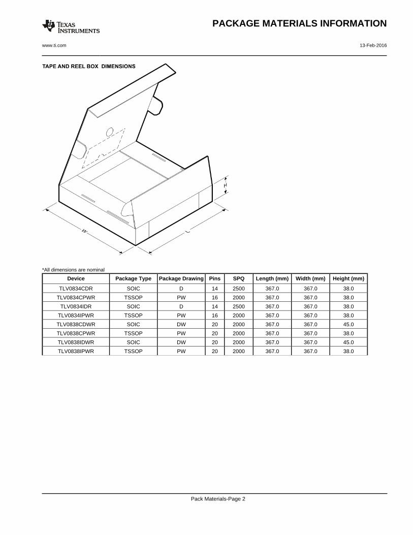
*All dimensions are nominal
Device Package Type Package Drawing Pins SPQ Length (mm) Width (mm) Height (mm)
TLV0834CDR SOIC D 14 2500 367.0 367.0 38.0
TLV0834CPWR TSSOP PW 16 2000 367.0 367.0 38.0
TLV0834IDR SOIC D 14 2500 367.0 367.0 38.0
TLV0834IPWR TSSOP PW 16 2000 367.0 367.0 38.0
TLV0838CDWR SOIC DW 20 2000 367.0 367.0 45.0
TLV0838CPWR TSSOP PW 20 2000 367.0 367.0 38.0
TLV0838IDWR SOIC DW 20 2000 367.0 367.0 45.0
TLV0838IPWR TSSOP PW 20 2000 367.0 367.0 38.0
PACKAGE MATERIALS INFORMATION
www.ti.com 13-Feb-2016
Pack Materials-Page 2
www.ti.com
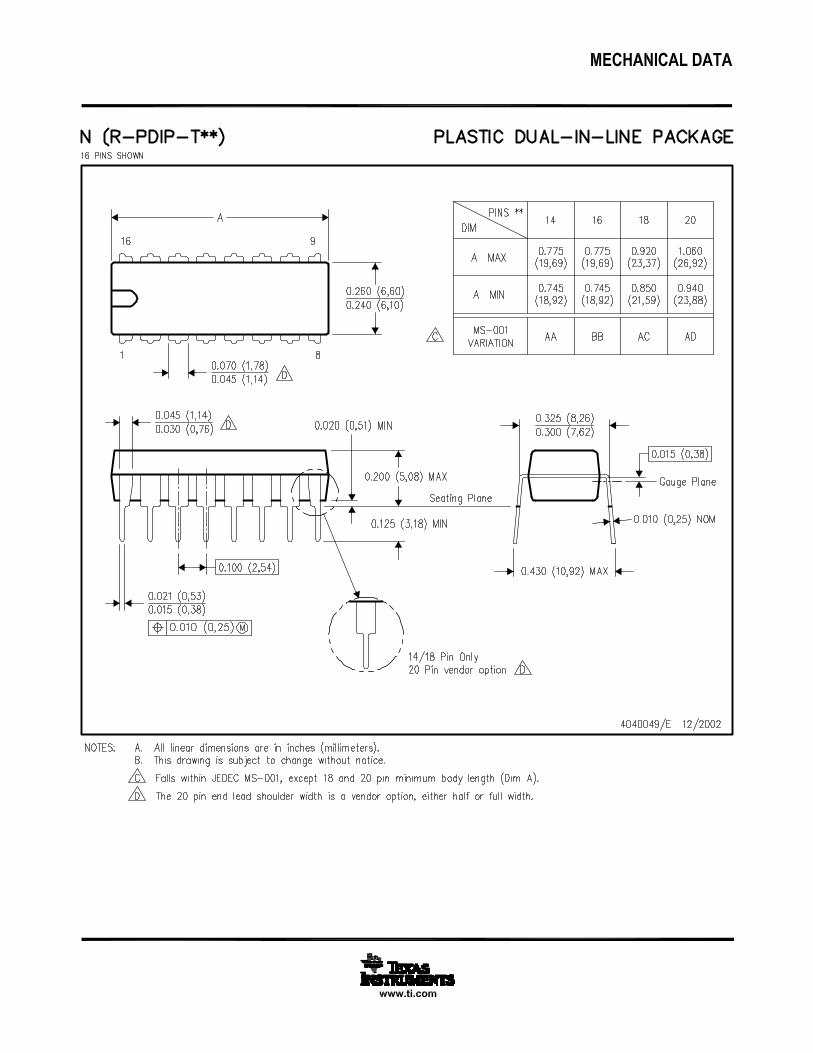
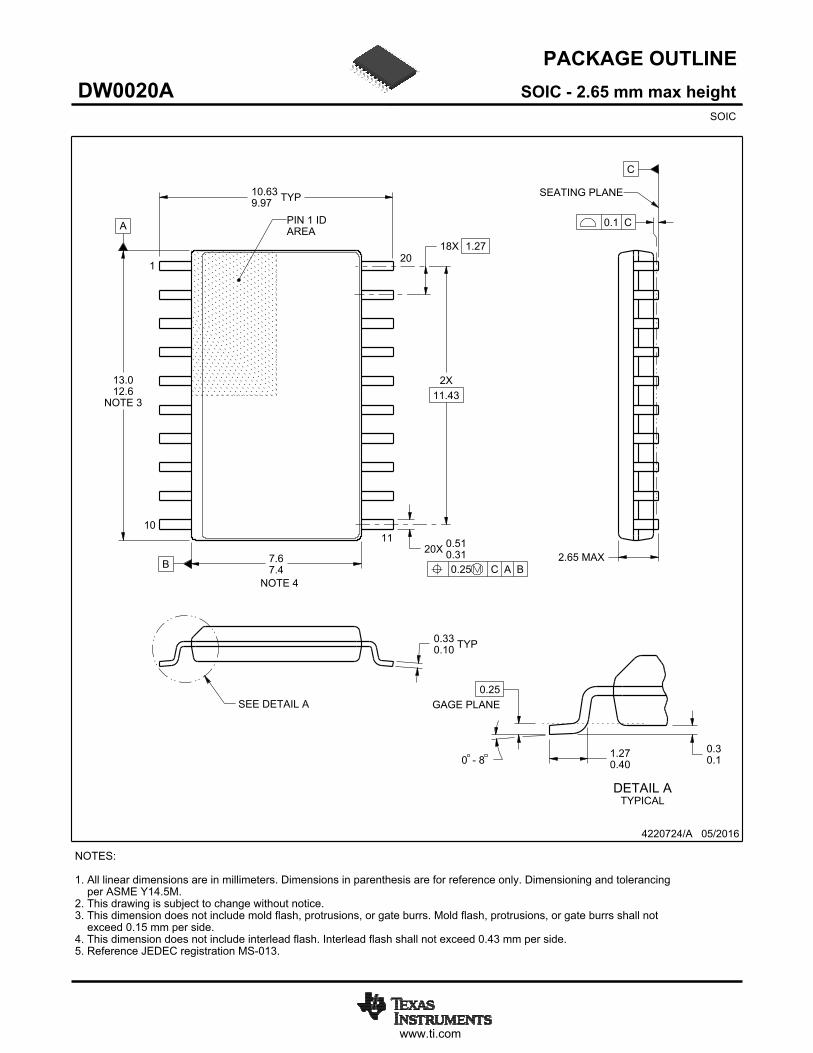
PACKAGE OUTLINE
C
TYP10.639.97
2.65 MAX
18X 1.27
20X 0.510.31
2X11.43
TYP0.330.10
0 - 80.30.1
0.25GAGE PLANE
1.270.40
A
NOTE 3
13.012.6
B 7.67.4
4220724/A 05/2016
SOIC - 2.65 mm max heightDW0020ASOIC
NOTES: 1. All linear dimensions are in millimeters. Dimensions in parenthesis are for reference only. Dimensioning and tolerancing per ASME Y14.5M. 2. This drawing is subject to change without notice. 3. This dimension does not include mold flash, protrusions, or gate burrs. Mold flash, protrusions, or gate burrs shall not exceed 0.15 mm per side. 4. This dimension does not include interlead flash. Interlead flash shall not exceed 0.43 mm per side.5. Reference JEDEC registration MS-013.
120
0.25 C A B
1110
PIN 1 IDAREA
NOTE 4
SEATING PLANE
0.1 C
SEE DETAIL A
DETAIL ATYPICAL
SCALE 1.200
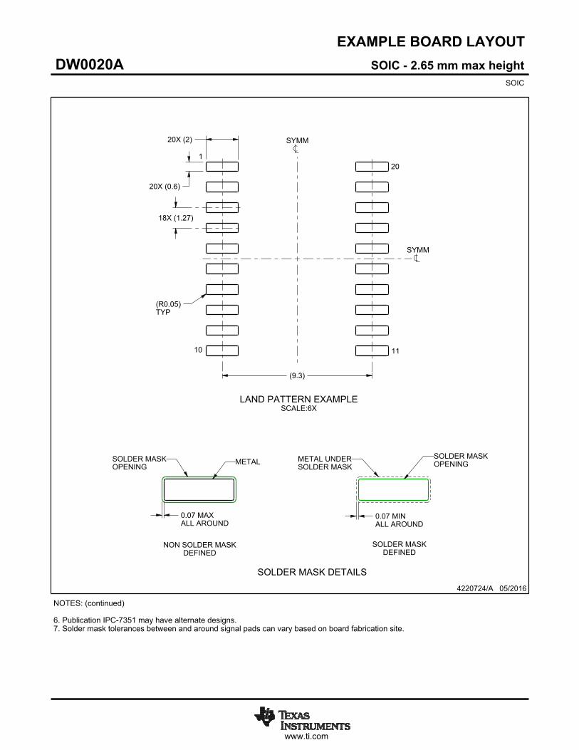
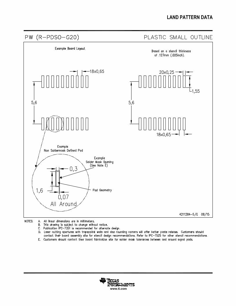
www.ti.com
EXAMPLE BOARD LAYOUT
(9.3)
0.07 MAXALL AROUND
0.07 MINALL AROUND
20X (2)
20X (0.6)
18X (1.27)
(R )TYP
0.05
4220724/A 05/2016
SOIC - 2.65 mm max heightDW0020ASOIC
SYMM
SYMM
LAND PATTERN EXAMPLESCALE:6X
1
10 11
20
NOTES: (continued) 6. Publication IPC-7351 may have alternate designs. 7. Solder mask tolerances between and around signal pads can vary based on board fabrication site.
METALSOLDER MASKOPENING
NON SOLDER MASKDEFINED
SOLDER MASK DETAILS
SOLDER MASKOPENING
METAL UNDERSOLDER MASK
SOLDER MASKDEFINED
www.ti.com
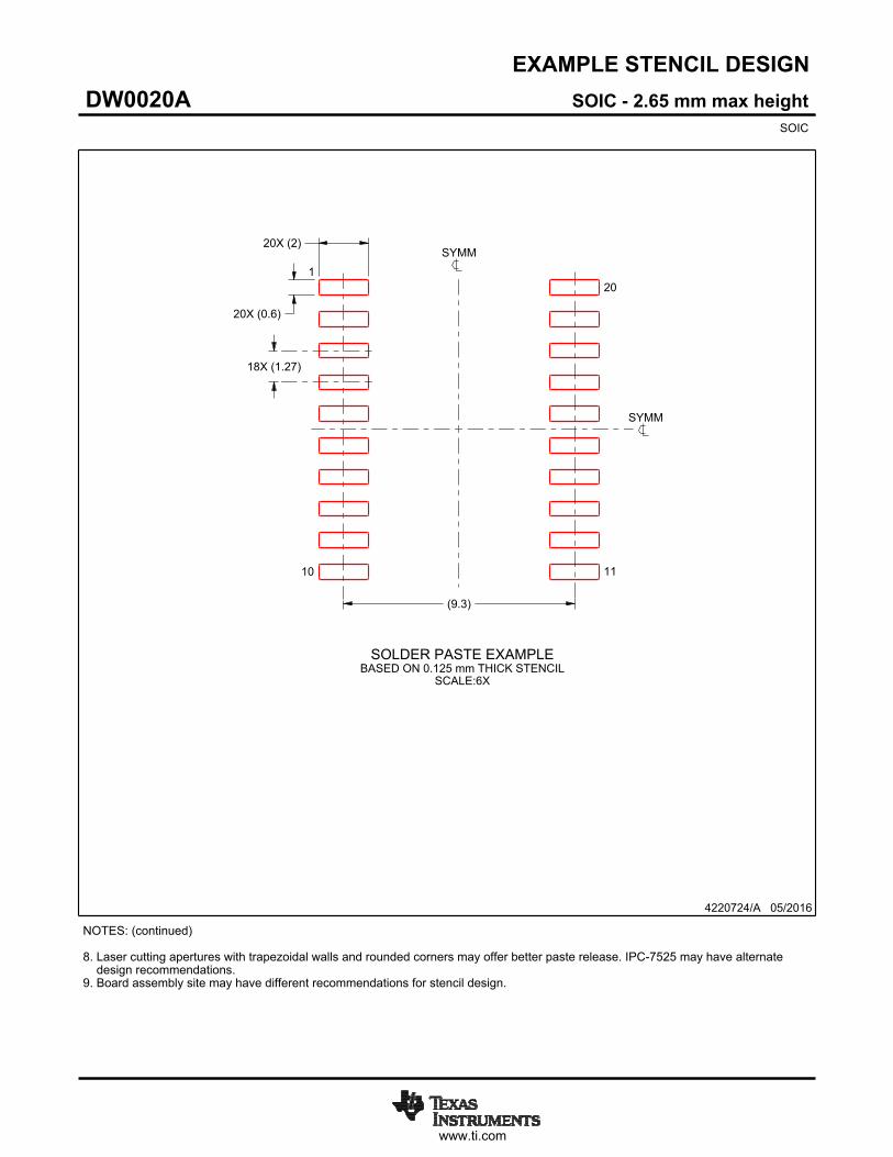
EXAMPLE STENCIL DESIGN
(9.3)
18X (1.27)
20X (0.6)
20X (2)
4220724/A 05/2016
SOIC - 2.65 mm max heightDW0020ASOIC
NOTES: (continued) 8. Laser cutting apertures with trapezoidal walls and rounded corners may offer better paste release. IPC-7525 may have alternate design recommendations. 9. Board assembly site may have different recommendations for stencil design.
SYMM
SYMM
1
10 11
20
SOLDER PASTE EXAMPLEBASED ON 0.125 mm THICK STENCIL
SCALE:6X
IMPORTANT NOTICE
Texas Instruments Incorporated (TI) reserves the right to make corrections, enhancements, improvements and other changes to itssemiconductor products and services per JESD46, latest issue, and to discontinue any product or service per JESD48, latest issue. Buyersshould obtain the latest relevant information before placing orders and should verify that such information is current and complete.TI’s published terms of sale for semiconductor products (http://www.ti.com/sc/docs/stdterms.htm) apply to the sale of packaged integratedcircuit products that TI has qualified and released to market. Additional terms may apply to the use or sale of other types of TI products andservices.Reproduction of significant portions of TI information in TI data sheets is permissible only if reproduction is without alteration and isaccompanied by all associated warranties, conditions, limitations, and notices. TI is not responsible or liable for such reproduceddocumentation. Information of third parties may be subject to additional restrictions. Resale of TI products or services with statementsdifferent from or beyond the parameters stated by TI for that product or service voids all express and any implied warranties for theassociated TI product or service and is an unfair and deceptive business practice. TI is not responsible or liable for any such statements.Buyers and others who are developing systems that incorporate TI products (collectively, “Designers”) understand and agree that Designersremain responsible for using their independent analysis, evaluation and judgment in designing their applications and that Designers havefull and exclusive responsibility to assure the safety of Designers' applications and compliance of their applications (and of all TI productsused in or for Designers’ applications) with all applicable regulations, laws and other applicable requirements. Designer represents that, withrespect to their applications, Designer has all the necessary expertise to create and implement safeguards that (1) anticipate dangerousconsequences of failures, (2) monitor failures and their consequences, and (3) lessen the likelihood of failures that might cause harm andtake appropriate actions. Designer agrees that prior to using or distributing any applications that include TI products, Designer willthoroughly test such applications and the functionality of such TI products as used in such applications.TI’s provision of technical, application or other design advice, quality characterization, reliability data or other services or information,including, but not limited to, reference designs and materials relating to evaluation modules, (collectively, “TI Resources”) are intended toassist designers who are developing applications that incorporate TI products; by downloading, accessing or using TI Resources in anyway, Designer (individually or, if Designer is acting on behalf of a company, Designer’s company) agrees to use any particular TI Resourcesolely for this purpose and subject to the terms of this Notice.TI’s provision of TI Resources does not expand or otherwise alter TI’s applicable published warranties or warranty disclaimers for TIproducts, and no additional obligations or liabilities arise from TI providing such TI Resources. TI reserves the right to make corrections,enhancements, improvements and other changes to its TI Resources. TI has not conducted any testing other than that specificallydescribed in the published documentation for a particular TI Resource.Designer is authorized to use, copy and modify any individual TI Resource only in connection with the development of applications thatinclude the TI product(s) identified in such TI Resource. NO OTHER LICENSE, EXPRESS OR IMPLIED, BY ESTOPPEL OR OTHERWISETO ANY OTHER TI INTELLECTUAL PROPERTY RIGHT, AND NO LICENSE TO ANY TECHNOLOGY OR INTELLECTUAL PROPERTYRIGHT OF TI OR ANY THIRD PARTY IS GRANTED HEREIN, including but not limited to any patent right, copyright, mask work right, orother intellectual property right relating to any combination, machine, or process in which TI products or services are used. Informationregarding or referencing third-party products or services does not constitute a license to use such products or services, or a warranty orendorsement thereof. Use of TI Resources may require a license from a third party under the patents or other intellectual property of thethird party, or a license from TI under the patents or other intellectual property of TI.TI RESOURCES ARE PROVIDED “AS IS” AND WITH ALL FAULTS. TI DISCLAIMS ALL OTHER WARRANTIES ORREPRESENTATIONS, EXPRESS OR IMPLIED, REGARDING RESOURCES OR USE THEREOF, INCLUDING BUT NOT LIMITED TOACCURACY OR COMPLETENESS, TITLE, ANY EPIDEMIC FAILURE WARRANTY AND ANY IMPLIED WARRANTIES OFMERCHANTABILITY, FITNESS FOR A PARTICULAR PURPOSE, AND NON-INFRINGEMENT OF ANY THIRD PARTY INTELLECTUALPROPERTY RIGHTS. TI SHALL NOT BE LIABLE FOR AND SHALL NOT DEFEND OR INDEMNIFY DESIGNER AGAINST ANY CLAIM,INCLUDING BUT NOT LIMITED TO ANY INFRINGEMENT CLAIM THAT RELATES TO OR IS BASED ON ANY COMBINATION OFPRODUCTS EVEN IF DESCRIBED IN TI RESOURCES OR OTHERWISE. IN NO EVENT SHALL TI BE LIABLE FOR ANY ACTUAL,DIRECT, SPECIAL, COLLATERAL, INDIRECT, PUNITIVE, INCIDENTAL, CONSEQUENTIAL OR EXEMPLARY DAMAGES INCONNECTION WITH OR ARISING OUT OF TI RESOURCES OR USE THEREOF, AND REGARDLESS OF WHETHER TI HAS BEENADVISED OF THE POSSIBILITY OF SUCH DAMAGES.Unless TI has explicitly designated an individual product as meeting the requirements of a particular industry standard (e.g., ISO/TS 16949and ISO 26262), TI is not responsible for any failure to meet such industry standard requirements.Where TI specifically promotes products as facilitating functional safety or as compliant with industry functional safety standards, suchproducts are intended to help enable customers to design and create their own applications that meet applicable functional safety standardsand requirements. Using products in an application does not by itself establish any safety features in the application. Designers mustensure compliance with safety-related requirements and standards applicable to their applications. Designer may not use any TI products inlife-critical medical equipment unless authorized officers of the parties have executed a special contract specifically governing such use.Life-critical medical equipment is medical equipment where failure of such equipment would cause serious bodily injury or death (e.g., lifesupport, pacemakers, defibrillators, heart pumps, neurostimulators, and implantables). Such equipment includes, without limitation, allmedical devices identified by the U.S. Food and Drug Administration as Class III devices and equivalent classifications outside the U.S.TI may expressly designate certain products as completing a particular qualification (e.g., Q100, Military Grade, or Enhanced Product).Designers agree that it has the necessary expertise to select the product with the appropriate qualification designation for their applicationsand that proper product selection is at Designers’ own risk. Designers are solely responsible for compliance with all legal and regulatoryrequirements in connection with such selection.Designer will fully indemnify TI and its representatives against any damages, costs, losses, and/or liabilities arising out of Designer’s non-compliance with the terms and provisions of this Notice.
Mailing Address: Texas Instruments, Post Office Box 655303, Dallas, Texas 75265Copyright © 2017, Texas Instruments Incorporated