Embed Size (px)
Citation preview
_______________________________________________________________ Maxim Integrated Products 1
For pricing, delivery, and ordering information, please contact Maxim Direct at 1-888-629-4642, or visit Maxim’s website at www.maxim-ic.com.
28V-Capable, ILIM VBUS Accessory Switch
MA
X1
45
44
/MA
X1
45
45
General DescriptionThe MAX14544/MAX14545 are overcurrent detection switches that can provide power to external accesso-ries while preventing the host device from damage due to faulty overload conditions. These analog switches feature a 270mω (typ) on-resistance and operate from a +2.3V to +5.5V input voltage range. The selectable current limit of 200mA or 400mA makes them ideal for load-switching applications.
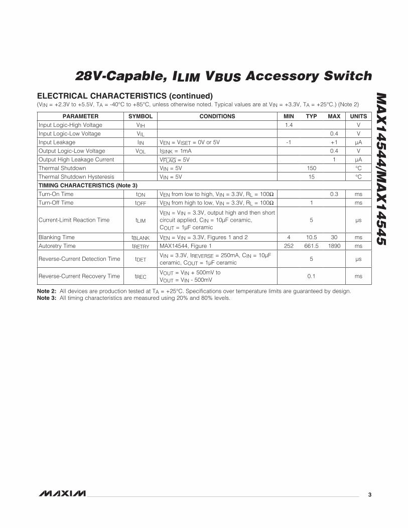
The MAX14544 has an autoretry feature, whereas the MAX14545 has a latchoff feature. When the switch is off, OUT can withstand 28V maximum. When the switch is on and a load is connected to the port, a blanking time of 10.5ms ensures that the transient voltage settles down. After this blanking time, if the voltage across the switch is greater than the FLAG assertion voltage, the switch turns off and then a FLAG is issued to the microprocessor. After the retry time, the device recloses for the duration of the blanking time to check if the load current is lower than the limit. The MAX14544 repeats this cycle if the overload condition is present. During the cycle, FLAG remains asserted. The MAX14544 remains on after the overload condition is removed and FLAG deasserts. For the MAX14545, after the blanking time, the switch turns off and then a FLAG is issued to the microprocessor. The switch can be turned on again by cycling the power or the EN input.
The MAX14544/MAX14545 have additional safety fea-tures that include thermal shutdown protection, reverse-current blocking, and overvoltage protection.
The MAX14544/MAX14545 are offered in a space-sav-ing, 8-pin, 2mm x 2mm TDFN package, and operate over the -40NC to +85NC extended temperature range.
ApplicationsCell Phones
MP3 Players
PDAs
Digital Cameras
eBook
MID
Features
S 200mA or 400mA Selectable Current Limit
S Output Capable of Withstanding +28V
S Reverse-Current Shutdown Protection
S +2.3V to +5.5V Input Operation Range
S Undervoltage Lockout
S Autoretry or Latchoff Option
S Thermal Shutdown Protection
S 0.1µA (typ) Shutdown Current
S 5µs Fast Current-Limit Detect
S 8-Pin TDFN (2mm x 2mm) Package
S -40NC to +85NC Operating Temperature Range
19-5037; Rev 0; 1/10
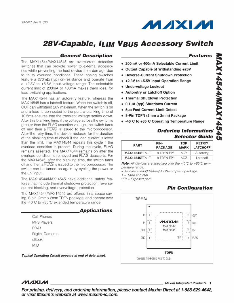
Pin Configuration
Ordering Information/Selector Guide
Note: All devices are specified over the -40°C to +85°C tem-perature range.+Denotes a lead(Pb)-free/RoHS-compliant package.T = Tape and reel.*EP = Exposed pad.
Typical Operating Circuit appears at end of data sheet.
1
+
*EP
*CONNECT EXPOSED PAD TO GND.
3
4
8
6
5
OUT
2 7 OUT
IN
ISET
GND
IN
TDFN
MAX14544MAX14545
TOP VIEW
EN
FLAG
PARTPIN-PACKAGE
TOP MARK
RETRY/LATCHOFF
MAX14544ETA+T 8 TDFN-EP* ACY Autoretry
MAX14545ETA+T 8 TDFN-EP* ACZ Latchoff
28V-Capable, ILIM VBUS Accessory Switch
MA
X1
45
44
/MA
X1
45
45
2
Stresses beyond those listed under “Absolute Maximum Ratings” may cause permanent damage to the device. These are stress ratings only, and functional operation of the device at these or any other conditions beyond those indicated in the operational sections of the specifications is not implied. Exposure to absolute maximum rating conditions for extended periods may affect device reliability.
(Voltages referenced to GND.)OUT .......................................................................-0.3V to +30VIN, FLAG, EN, ISET ..............................................-0.3V to +6.0VContinuous Power Dissipation (TA = +70NC) 8-Pin TDFN (derate 11.9mW/NC above +70NC) ...........953mWJunction-to-Ambient Thermal Resistance BJA (Note 1) ..............................................................83.9NC/W
Junction-to-Case Thermal Resistance BJC (Note 1) .................................................................37NC/WOperating Temperature Range .......................... -40NC to +85NCStorage Temperature Range ............................ -65NC to +150NCJunction Temperature ..................................... -40NC to +150NCLead Temperature (soldering, 10s) ................................+300NCSoldering Temperature (reflow) ......................................+260NC
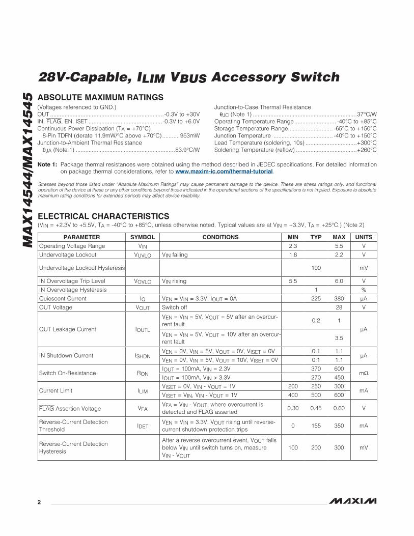
ELECTRICAL CHARACTERISTICS(VIN = +2.3V to +5.5V, TA = -40NC to +85NC, unless otherwise noted. Typical values are at VIN = +3.3V, TA = +25NC.) (Note 2)
ABSOLUTE MAXIMUM RATINGS
Note 1: Package thermal resistances were obtained using the method described in JEDEC specifications. For detailed information on package thermal considerations, refer to www.maxim-ic.com/thermal-tutorial.
PARAMETER SYMBOL CONDITIONS MIN TYP MAX UNITS
Operating Voltage Range VIN 2.3 5.5 V
Undervoltage Lockout VUVLO VIN falling 1.8 2.2 V
Undervoltage Lockout Hysteresis 100 mV
IN Overvoltage Trip Level VOVLO VIN rising 5.5 6.0 V
IN Overvoltage Hysteresis 1 %
Quiescent Current IQ VEN = VIN = 3.3V, IOUT = 0A 225 380 FA
OUT Voltage VOUT Switch off 28 V
OUT Leakage Current IOUTL
VEN = VIN = 5V, VOUT = 5V after an overcur-rent fault
0.2 1
FAVEN = VIN = 5V, VOUT = 10V after an overcur-rent fault
3.5
IN Shutdown Current ISHDNVEN = 0V, VIN = 5V, VOUT = 0V, VISET = 0V 0.1 1.1
FAVEN = 0V, VIN = 5V, VOUT = 10V, VISET = 0V 0.1 1.1
Switch On-Resistance RONIOUT = 100mA, VIN = 2.3V 370 600
mIIOUT = 100mA, VIN > 3.3V 270 450
Current Limit ILIMVISET = 0V, VIN - VOUT = 1V 200 250 300
mAVISET = VIN, VIN - VOUT = 1V 400 500 600
FLAG Assertion Voltage VFAVFA = VIN - VOUT, where overcurrent is detected and FLAG asserted
0.30 0.45 0.60 V
Reverse-Current Detection Threshold
IDETVEN = VIN = 3.3V, VOUT rising until reverse- current shutdown protection trips
0 155 350 mA
Reverse-Current Detection Hysteresis
After a reverse overcurrent event, VOUT falls below VIN until switch turns on, measure VIN - VOUT
100 200 300 mV
28V-Capable, ILIM VBUS Accessory Switch
MA
X1
45
44
/MA
X1
45
45
3
ELECTRICAL CHARACTERISTICS (continued)(VIN = +2.3V to +5.5V, TA = -40NC to +85NC, unless otherwise noted. Typical values are at VIN = +3.3V, TA = +25NC.) (Note 2)
Note 2: All devices are production tested at TA = +25NC. Specifications over temperature limits are guaranteed by design.Note 3: All timing characteristics are measured using 20% and 80% levels.
PARAMETER SYMBOL CONDITIONS MIN TYP MAX UNITS
Input Logic-High Voltage VIH 1.4 V
Input Logic-Low Voltage VIL 0.4 V
Input Leakage IIN VEN = VISET = 0V or 5V -1 +1 FA
Output Logic-Low Voltage VOL ISINK = 1mA 0.4 V
Output High Leakage Current VFLAG = 5V 1 FA
Thermal Shutdown VIN = 5V 150 NC
Thermal Shutdown Hysteresis VIN = 5V 15 NC
TIMING CHARACTERISTICS (Note 3)
Turn-On Time tON VEN from low to high, VIN = 3.3V, RL = 100I 0.3 ms
Turn-Off Time tOFF VEN from high to low, VIN = 3.3V, RL = 100I 1 ms
Current-Limit Reaction Time tLIM
VEN = VIN = 3.3V, output high and then short circuit applied, CIN = 10FF ceramic,COUT = 1FF ceramic
5 Fs
Blanking Time tBLANK VEN = VIN = 3.3V, Figures 1 and 2 4 10.5 30 ms
Autoretry Time tRETRY MAX14544, Figure 1 252 661.5 1890 ms
Reverse-Current Detection Time tDETVIN = 3.3V, IREVERSE = 250mA, CIN = 10FF ceramic, COUT = 1FF ceramic
5 Fs
Reverse-Current Recovery Time tRECVOUT = VIN + 500mV to VOUT = VIN - 500mV
0.1 ms
28V-Capable, ILIM VBUS Accessory Switch
MA
X1
45
44
/MA
X1
45
45
4
Figure 1. MAX14544 Timing Diagram (Waveforms Not to Scale)
Figure 2. MAX14545 Timing Diagram (Waveforms Not to Scale)
tBLANK tBLANK tBLANK tBLANKtRETRY tRETRY
CURRENT LIMIT
LOAD CURRENT
ON
OFF
EN
ON
OFF
SWITCH
FLAG
CURRENT LIMIT
LOAD CURRENT
ON
OFF
EN
ON
OFF
SWITCH
FLAG
tBLANK tBLANK
28V-Capable, ILIM VBUS Accessory Switch
MA
X1
45
44
/MA
X1
45
45
5
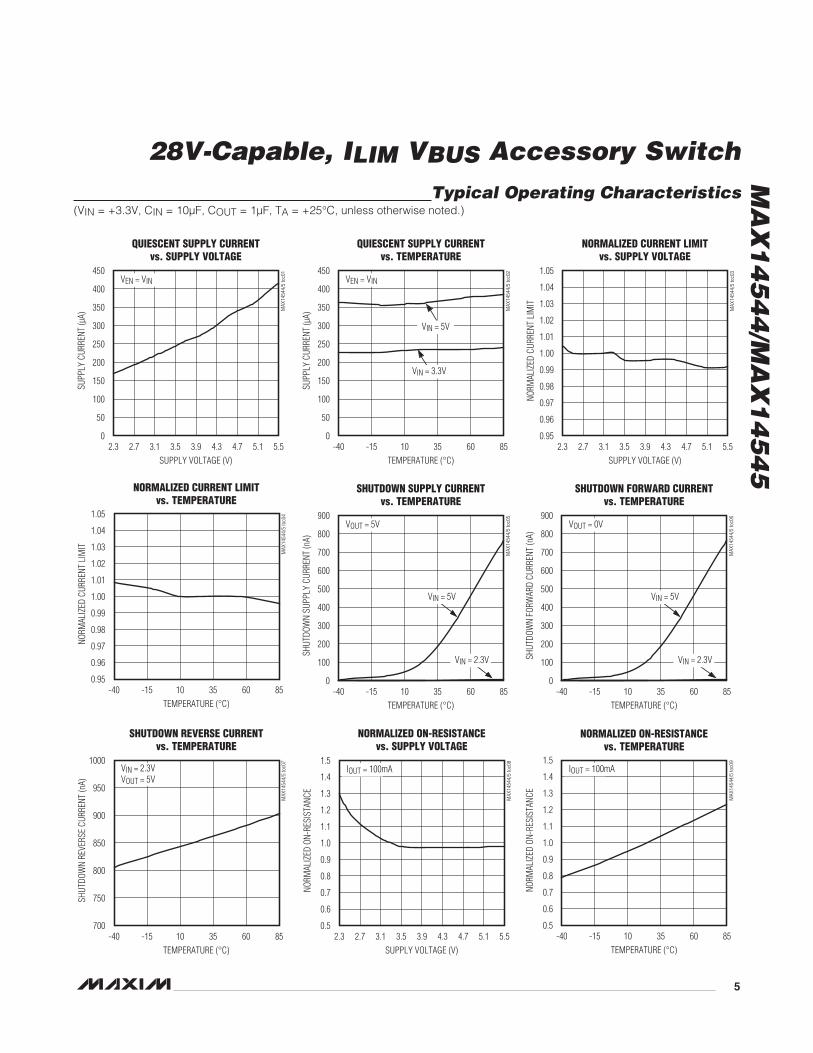
Typical Operating Characteristics(VIN = +3.3V, CIN = 10FF, COUT = 1FF, TA = +25NC, unless otherwise noted.)
NORMALIZED ON-RESISTANCEvs. TEMPERATURE
MAX
1454
4/5
toc0
9
TEMPERATURE (°C)
NORM
ALIZ
ED O
N-RE
SIST
ANCE
603510-15
0.6
0.7
0.8
0.9
1.0
1.1
1.2
1.3
1.4
1.5
0.5-40 85
IOUT = 100mA
NORMALIZED ON-RESISTANCEvs. SUPPLY VOLTAGE
MAX
1454
4/5
toc0
8
SUPPLY VOLTAGE (V)
NORM
ALIZ
ED O
N-RE
SIST
ANCE
5.14.73.9 4.33.1 3.52.7
0.6
0.7
0.8
0.9
1.0
1.1
1.2
1.3
1.4
1.5
0.52.3 5.5
IOUT = 100mA
SHUTDOWN REVERSE CURRENTvs. TEMPERATURE
MAX
1454
4/5
toc0
7
TEMPERATURE (°C)
SHUT
DOW
N RE
VERS
E CU
RREN
T (n
A)
603510-15
750
800
850
900
950
1000
700-40 85
VIN = 2.3VVOUT = 5V
SHUTDOWN FORWARD CURRENTvs. TEMPERATURE
MAX
1454
4/5
toc0
6
TEMPERATURE (°C)
SHUT
DOW
N FO
RWAR
D CU
RREN
T (n
A)
603510-15
100
200
300
400
500
600
700
800
900
0-40 85
VOUT = 0V
VIN = 5V
VIN = 2.3V
SHUTDOWN SUPPLY CURRENTvs. TEMPERATURE
MAX
1454
4/5
toc0
5
TEMPERATURE (°C)
SHUT
DOW
N SU
PPLY
CUR
RENT
(nA)
603510-15
100
200
300
400
500
600
700
800
900
0-40 85
VOUT = 5V
VIN = 5V
VIN = 2.3V
NORMALIZED CURRENT LIMITvs. TEMPERATURE
MAX
1454
4/5
toc0
4
TEMPERATURE (°C)
NORM
ALIZ
ED C
URRE
NT L
IMIT
603510-15
0.96
0.97
0.98
0.99
1.00
1.01
1.02
1.03
1.04
1.05
0.95-40 85
NORMALIZED CURRENT LIMITvs. SUPPLY VOLTAGE
MAX
1454
4/5
toc0
3
SUPPLY VOLTAGE (V)
NORM
ALIZ
ED C
URRE
NT L
IMIT
5.14.73.9 4.33.1 3.52.7
0.96
0.97
0.98
0.99
1.00
1.01
1.02
1.03
1.04
1.05
0.952.3 5.5
QUIESCENT SUPPLY CURRENTvs. TEMPERATURE
MAX
1454
4/5
toc0
2
TEMPERATURE (°C)
SUPP
LY C
URRE
NT (µ
A)
603510-15
50
100
150
200
250
300
350
400
450
0-40 85
VEN = VIN
VIN = 5V
VIN = 3.3V
QUIESCENT SUPPLY CURRENTvs. SUPPLY VOLTAGE
MAX
1454
4/5
toc0
1
SUPPLY VOLTAGE (V)
SUPP
LY C
URRE
NT (µ
A)
5.14.73.9 4.33.1 3.52.7
50
100
150
200
250
300
350
400
450
02.3 5.5
VEN = VIN
28V-Capable, ILIM VBUS Accessory Switch
MA
X1
45
44
/MA
X1
45
45
6
BLANKING TIMEMAX14544/5 toc18
10ms/div
VOUT2V/div
IOUT200mA/div
VFLAG2V/div
MAX14544 ISET HIGH
OVERCURRENT DURATION TIMEMAX14544/5 toc17
200ms/div
VOUT2V/div
IOUT200mA/div
VFLAG2V/div
MAX14544 ISET HIGH
CURRENT LIMIT RESPONSEMAX14544/5 toc16
100ms/div
VOUT2V/div
IOUT200mA/div
VFLAG2V/div
ISET HIGH
CURRENT LIMIT RESPONSEMAX14544/5 toc15
20ms/div
VOUT2V/div
IOUT200mA/div
VFLAG2V/div
ISET HIGH
FLAG RESPONSEMAX14544/5 toc14
100ms/div
VOUT5V/div
IOUT200mA/div
VFLAG5V/div
VIN = 5VRL = 100ΩISET HIGH
REVERSE OVERVOLTAGE PROTECTIONMAX14544/5 toc13
10µs/div
10V
5V
0V
0V
3.3V
VOUT2V/div
VIN2V/div
VEN = 0V
POWER-UP RESPONSEMAX14544/5 toc12
200µs/div
VIN5V/div
VOUT5V/div
IOUT50mA/div
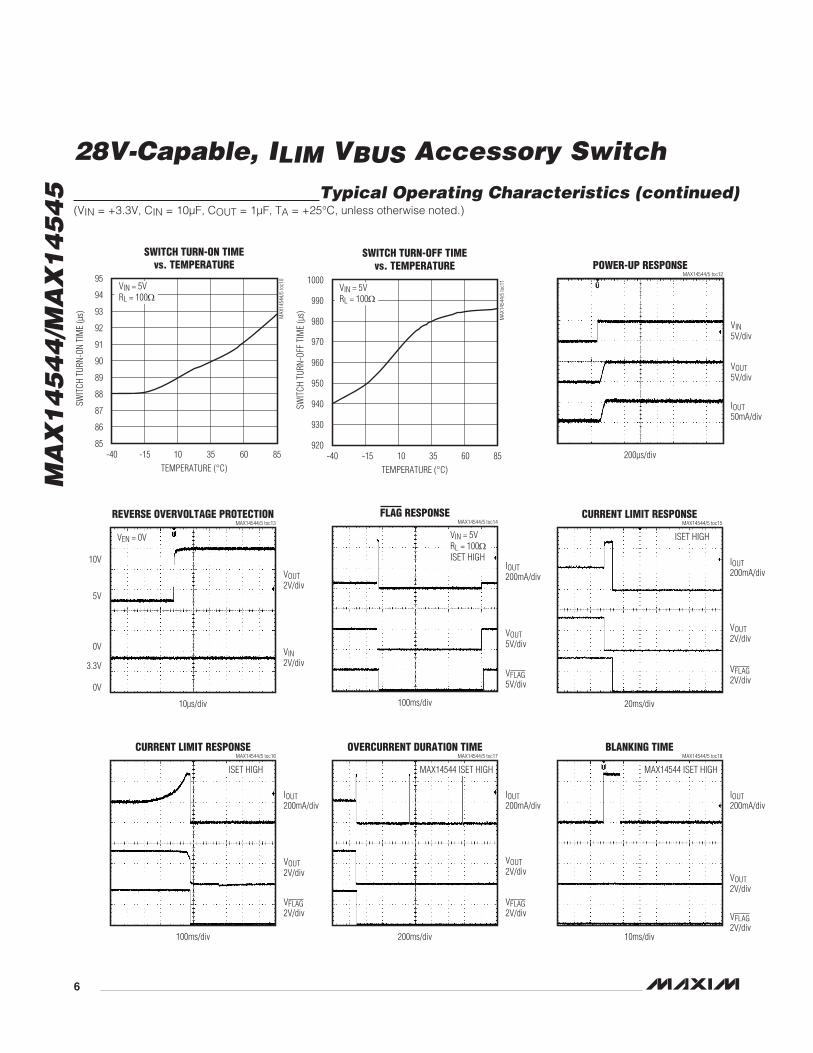
SWITCH TURN-OFF TIMEvs. TEMPERATURE
MAX
1454
4/5
toc1
1
TEMPERATURE (°C)
SWIT
CH T
URN-
OFF
TIM
E (µ
s)
6035-15 10
930
940
950
960
980
970
990
1000
920-40 85
VIN = 5VRL = 100Ω
SWITCH TURN-ON TIMEvs. TEMPERATURE
MAX
1454
4/5
toc1
0
TEMPERATURE (°C)
SWIT
CH T
URN-
ON T
IME
(µs)
603510-15
86
87
88
89
90
91
92
93
94
95
85-40 85
VIN = 5VRL = 100Ω
Typical Operating Characteristics (continued)(VIN = +3.3V, CIN = 10FF, COUT = 1FF, TA = +25NC, unless otherwise noted.)
28V-Capable, ILIM VBUS Accessory Switch
MA
X1
45
44
/MA
X1
45
45
7
Pin Description
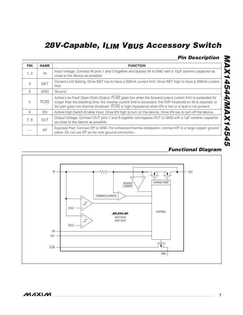
Functional Diagram
CONTROL
OVLO
EN
IN
ISET
CHARGE PUMP
OUT
GND
FORWARD CURRENT
REVERSECURRENT
MAX14544MAX14545
FLAG
UVLO
PIN NAME FUNCTION
1, 2 INInput Voltage. Connect IN pins 1 and 2 together and bypass IN to GND with a 10FF ceramic capacitor as close to the device as possible.
3 ISETCurrent-Limit Setting. Drive ISET low to have a 200mA current limit. Drive ISET high to have a 400mA current limit.
4 GND Ground
5 FLAGActive-Low Fault Open-Drain Output. FLAG goes low when the forward output current limit is exceeded for longer than the blanking time, the reverse current limit is exceeded, the OVP threshold on IN is reached, or the part goes into thermal shutdown. FLAG is high impedance when EN is low or a fault is not present.
6 EN Active-High Switch-Enable Input. Drive EN high to turn on the device. Drive EN low to turn off the device.
7, 8 OUTOutput Voltage. Connect OUT pins 7 and 8 together and bypass OUT to GND with a 1FF ceramic capacitor as close to the device as possible.
— EPExposed Pad. Connect EP to GND. For enhanced thermal dissipation, connect EP to a large copper ground plane. Do not use EP as the sole ground connection.
28V-Capable, ILIM VBUS Accessory Switch
MA
X1
45
44
/MA
X1
45
45
8
Detailed DescriptionThe MAX14544/MAX14545 are overcurrent detection switches that prevent host devices from being damaged due to faulty load conditions. The switch opens if current exceeds the current limit for longer than the blanking time or if a reverse-current condition is detected. The switch also disconnects if VIN exceeds OVLO, VIN falls below UVLO, thermal shutdown occurs, or EN is driven low. Current limit can be set to either 200mA or 400mA. When the switch is open, the output (OUT) can withstand 28V maximum.
When the switch is on and a load is connected to the port, a blanking time of 10.5ms ensures that the inrush current settles down. After this blanking time, if the volt-age across the switch is greater than the FLAG asser-tion voltage, the part is turned off and issues a FLAG to the microprocessor. After the retry time elapses, the MAX14544 switch is closed for the duration of the blank-ing time to check if the load current is lower than the limit. Cycle the power or EN input to turn the MAX14545 switch back on.
Current-Limit ThresholdThe MAX14544/MAX14545 ISET logic input sets the desired minimum current-limit threshold to 200mA or 400mA. Connect ISET low for a 200mA current limit and high for a 400mA current limit. If 400mA is selected as the current limit, the input supply current at shutdown can be reduced by connecting ISET to EN. This is due to the fact that the device consumes the lower supply current in ISET = low mode than in ISET = high mode.
Reverse-Current ProtectionThe MAX14544/MAX14545 monitor the reverse current (VOUT to VIN) from exceeding the maximum IDET value. If the reverse-current detection threshold is exceeded, the switch turns off and FLAG is asserted without waiting for tBLANK to elapse. This feature prevents excessive reverse currents from flowing through the device.
FLAG IndicatorThe MAX14544/MAX14545 feature a fault output (FLAG). Whenever VIN - VOUT > VFA, the MAX14544 asserts FLAG low after the blanking time and keeps it low until the condition is removed. During this time, the switch cycles on and off in the autoretry mode. When the condi-tion is removed, FLAG deasserts and the switch turns on (Figure 1). The MAX14545 asserts FLAG low after the blanking time and turns the switch off when FLAG asser-tion voltage is exceeded (Figure 2).
FLAG is an open-drain output and requires an external pullup resistor. During shutdown (EN is low), the pull-down on FLAG output is released to limit power dissipa-tion. FLAG goes low when one of the following occurs:
1) The temperature exceeds the thermal shutdown tem-perature, +150NC (typ).
2) The device is in current limit for more than the fault blanking period.
3) The switch is in autoretry.
4) The reverse current limit is exceeded.
5) The input is over the OVLO.
Autoretry (MAX14544)When the FLAG assertion voltage is exceeded, the tBLANK timer begins counting (Figure 1). The timer resets if the condition disappears before tBLANK has elapsed. A retry time delay (tRETRY) is started immediately after tBLANK has elapsed and during that time the switch is turned off and FLAG is asserted. At the end of tRETRY, the device is turned on again. If the fault still exists, the cycle is repeated. If the fault is removed, the device stays on and FLAG deasserts.
The autoretry feature saves system power in the case of a continuous overcurrent or short-circuit condition. During tBLANK, when the switch is on, the supply current is at the current limit. During tRETRY, when the switch is off, the current through the switch is zero. Instead of observing the full load current, the device sees the equivalent load current times duty cycle or:
ISUPPLY = ILOAD x tBLANK /(tBLANK + tRETRY)
With a typical tBLANK = 10.5ms and typical tRETRY = 661.5ms, the duty cycle is 1.6%, resulting in a 98.4% power savings over the switch being on the entire time.
Latchoff (MAX14545)When the FLAG assertion voltage is exceeded, the tBLANK timer begins counting. The device turns off after the blanking time. The timer resets if the condition is removed before the end of the blanking time. Reset the device by toggling EN (Figure 2).
Fault BlankingThe MAX14544/MAX14545 feature a 10.5ms (typ) fault blanking. Fault blanking allows current-limit faults, including momentary short-circuit faults that occur when plugging a capacitive load, and also ensures that no fault is issued during power-up. When a load transient causes the device to enter current limit, an internal coun-ter starts. If the load-transient fault persists beyond the
28V-Capable, ILIM VBUS Accessory Switch
MA
X1
45
44
/MA
X1
45
45
9
fault-blanking timeout, FLAG asserts low. FLAG is not asserted when load-transient fault is less than tBLANK. The fault blanking time only applies to forward current-limit faults.
A reverse current-limit fault, thermal fault, or OVP fault causes FLAG to assert immediately and does not wait for the blanking time.
Thermal ShutdownThe MAX14544/MAX14545 have a thermal-shutdown feature to protect the devices from overheating. The device turns off and FLAG goes low immediately (no fault blanking) when the junction temperature exceeds +150NC. The MAX14544/MAX14545 turns back on when the device temperature drops approximately 15NC.
OVLO and UVLOThe MAX14544/MAX14545 feature an overvoltage pro-tection. When IN goes above VOVLO (6.0V max), the switch turns off and FLAG goes low immediately with no fault-blanking time. When IN drops below VUVLO (1.8V min), the switch turns off but FLAG stays high. The MAX14544/MAX14545 turns back on when IN is in the operating range.
Applications InformationInput Capacitor
To limit the input-voltage drop during momentary output short-circuit conditions, connect a capacitor from IN to GND. A 10FF ceramic capacitor is adequate for most applications; however, higher capacitor values further reduce the voltage drop at the input and are recom-mended for lower voltage applications.
Output CapacitorConnect a 1FF ceramic capacitor from OUT to GND. This capacitor helps prevent inductive parasitics from pulling OUT negative during turn-off, thus preventing
the MAX14544/MAX14545 from tripping erroneously. If the load capacitance is too large, then current may not have enough time to charge the capacitance and the device assumes that there is faulty load condition. The maximum capacitive load value that can be driven from OUT is obtained by the following formula:
×< FWD_MIN BLANK_MIN
MAXIN
I tC
V
Layout and Thermal DissipationTo optimize the switch response time to output short-circuit conditions, it is very important to keep all traces as short as possible to reduce the effect of undesirable parasitic inductance. Place input and output capacitors as close as possible to the device. IN and OUT must be connected with short traces to the power bus.
During normal operation, the power dissipation is small and the package temperature change is minimal. If the output is continuously shorted to ground at the maximum supply voltage, the operation of the switches with the autoretry option does not cause problems because the total power dissipated during the short is scaled by the duty cycle:
IN_MAX OUT_MAX BLANKMAX
RETRY BLANK
V I tP 51.6mW
t t
× ×= =
+
where VIN_MAX = 5.5V, IOUT_MAX = 600mA, tBLANK = 10.5ms, and tRETRY = 661.5ms.
Attention must be given to the MAX14545 where the latchoff condition can be manually reset by toggling EN from high to low. If the latchoff time duration is not suf-ficiently high, it is possible for the device to reach the thermal-shutdown threshold and never be able to turn the device on until it cools down.
28V-Capable, ILIM VBUS Accessory Switch
MA
X1
45
44
/MA
X1
45
45
Maxim cannot assume responsibility for use of any circuitry other than circuitry entirely embodied in a Maxim product. No circuit patent licenses are implied. Maxim reserves the right to change the circuitry and specifications without notice at any time.
10 Maxim Integrated Products, 120 San Gabriel Drive, Sunnyvale, CA 94086 408-737-7600© 2010 Maxim Integrated Products Maxim is a registered trademark of Maxim Integrated Products, Inc.
Chip InformationPROCESS: BiCMOS
Package InformationFor the latest package outline information and land pat-terns, go to www.maxim-ic.com/packages. Note that a “+”, “#”, or “-” in the package code indicates RoHS status only. Package drawings may show a different suf-fix character, but the drawing pertains to the package regardless of RoHS status.
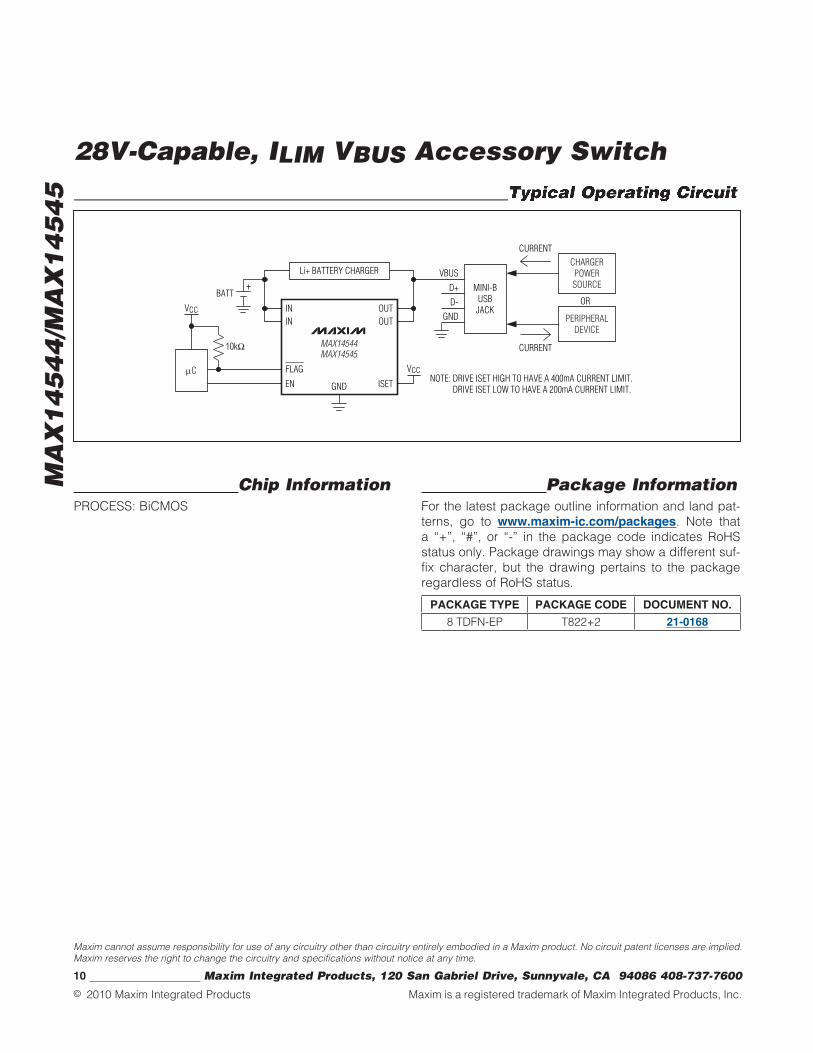
Typical Operating Circuit
Li+ BATTERY CHARGER
NOTE: DRIVE ISET HIGH TO HAVE A 400mA CURRENT LIMIT. DRIVE ISET LOW TO HAVE A 200mA CURRENT LIMIT.
MINI-BUSBJACKOUT
OUT
ISET
IN
BATT
10kI
VCC
IN
EN GND
VBUS
CURRENT
OR
CURRENT
D+
GND
D-
MAX14544MAX14545
µC
CHARGERPOWERSOURCE
PERIPHERALDEVICE
VCCFLAG
PACKAGE TYPE PACKAGE CODE DOCUMENT NO.
8 TDFN-EP T822+2 21-0168


![Untitled-6 [ilim-lib.narod.ru]ilim-lib.narod.ru/Chernyh_noty/Letuchaya_kosh.pdf · l. Komvxa 110KOH Mb1LL1atv[ He AaBana Cepb1M xwrb11aM qepnaKa rt0ABaJ1a. ee HaKä3aTb, eil r10Ka3aTb](https://img.pdfslide.us/doc/110x75/603876cd66cd4d56a07c1839/untitled-6-ilim-libnarodruilim-libnarodruchernyhnotyletuchayakoshpdf.jpg)