Embed Size (px)
Citation preview
DPS1133 Document number: DS39393 Rev. 6 - 2
1 of 16 www.diodes.com
April 2018 © Diodes Incorporated
DPS1133
24V/3A 1-CH POWER SWITCH WITH FAST ROLE SWAP
Description
The DPS1133 is part of a family of power switches optimized for the
USB Power Delivery and other hot-swap applications. Through the
analog interface, exception status is reported and several functions
can be programmed: current limit, overvoltage protection, and output
voltage ramping up. The fast role swap function which complies with
the requirements defined in the USB Power Delivery Specification
Release 3.0, V1.0a is implemented.
This device is designed to operate between 4.5V and 24V. It offers
fast short-circuit response time to ensure system robustness. The
integrated port-discharge function allows the voltage levels at the
input and output ports to be discharged to meet the requirements of
the USB Power Delivery Specification. Comprehensive fault detection
and recovery mechanisms are provisioned to enable applications
which are subjected to heavy capacitive loads and the risk of short
circuit. These mechanisms include: reverse voltage & current
blocking, input overvoltage protection, output overcurrent, short-circuit
protection and overtemperature shut-down. In addition, the rise time
of output voltage can be adjusted to minimize in-rush current and to
ensure system stability. Before any exception condition is notified via
the low-active FAULTB signal, deglitch of 7ms is applied to prevent
false triggering.
The DPS1133 is housed in the low-profile and space-saving V-
QFN4040-17 package which is manufactured with environmental-
friendly material.
Features
Wide Operating Voltage Range: 4.5V to 24V
1-channel Power Switch with Integrated Adjustable Current &
Voltage Limits
Ability to Discharge the Input and Output Ports either Individually
or Simultaneously via the Two External Control Pins
Fast Short-circuit Response Time at 2µs
Comprehensive Built-in Fault Detection and Recovery
Mechanisms like Input Undervoltage Lock-out, Reverse Voltage
& Current Blocking, Thermal Shut-down, Overcurrent and Short-
circuit Protection
RDS(ON) of Embedded MOSFET at 30mΩ
Adjustable DV/DT Control at Start-up
Fault Reporting (FAULTB) with Blanking Time at 7ms Typical
Fast Role Swap Supported
UL Recognized, File No. E322375
IEC60950-1 CB Scheme Certified
Totally Lead-Free & Fully RoHS Compliant (Notes 1 & 2)
Halogen and Antimony Free. “Green” Device (Note 3)
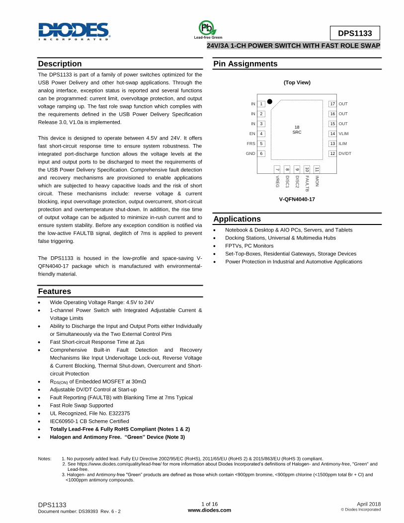
Pin Assignments
(Top View)
2
1
3
4
5
6
18
SRC
16
17
15
14
13
12
87 9 10
11
DIS
C1
IN
IN
IN
EN
FRS
GND
VR
EG
DIS
C2
FA
UL
TB
OUT
OUT
OUT
VLIM
ILIM
DV/DT
IMO
N
V-QFN4040-17
Applications
Notebook & Desktop & AIO PCs, Servers, and Tablets
Docking Stations, Universal & Multimedia Hubs
FPTVs, PC Monitors
Set-Top-Boxes, Residential Gateways, Storage Devices
Power Protection in Industrial and Automotive Applications
Notes: 1. No purposely added lead. Fully EU Directive 2002/95/EC (RoHS), 2011/65/EU (RoHS 2) & 2015/863/EU (RoHS 3) compliant. 2. See https://www.diodes.com/quality/lead-free/ for more information about Diodes Incorporated’s definitions of Halogen- and Antimony-free, "Green" and Lead-free.
3. Halogen- and Antimony-free "Green” products are defined as those which contain <900ppm bromine, <900ppm chlorine (<1500ppm total Br + Cl) and <1000ppm antimony compounds.
DPS1133 Document number: DS39393 Rev. 6 - 2
2 of 16 www.diodes.com
April 2018 © Diodes Incorporated
DPS1133
Typical Application Circuit
DPS1133
1
2
3
4
5
6
987 10
11
IN
IN
IN
EN
FRS
GND VR
EG
DIS
C1
FA
ULT
B
DIS
C2
17
16
15
14
13
12
OUT
OUT
OUT
VLIM
ILIM
DV/DTIMO
N
RVLIM
220kΩRILIM
30kΩCDV/DT
1nF
COUT
10μFCIN
10μF
RPU
10kΩ
3.3V
OFF
ON
VEN
VFRS
VD
ISC
1
VD
ISC
2CVREG
0.1μF
VIN VOUT
SRC
18
VS
RC
RIMON
100kΩ
DOUT
Schottky Diode
CIMON
100pF
CFLT
0.1uF
Pin Descriptions
Pin Number Pin Name Type Function
1, 2, 3 IN P Power Supply and Input port.
4 EN I Enable Input. Active high. ‘0’ = Device OFF; ‘1’ = Device ON. This pin shall not be left floating.
5 FRS I Fast Role Swap Control. This pin enables the Fast Role Swap sequence defined in the USB Power
Delivery Specification Release 3.0, V1.0a.
6 GND GND Device Ground.
7 VREG I/O Voltage Regulator. A 0.1µF is recommended between this pin and GND.
8 DISC1 I IN Port Discharge Control. ‘1’ = port voltage to be discharged; ‘0’ = disabled.
9 DISC2 I OUT Port Discharge Control. ‘1’ = port voltage to be discharged; ‘0’ = disabled.
10 FAULTB O Fault Status Indicator. An external pull-up resistor is required. This active-low pin shall be tied to
GND when not used.
11 IMON O
Current Monitor. A 100pF capacitor and a resistor connected in parallel between this pin and GND
creates a positive average voltage proportional to the current flowing through the device. This pin
can be left floating if current monitoring is not needed.
12 DV/DT I/O Ramp-up Control. A capacitor between this pin and GND sets the ramp-up rate.
13 ILIM I/O Current Limit Setting. A resistor between this pin and GND sets the overcurrent limit of the OUT
port.
14 VLIM I/O Voltage Limit Setting. A resistor between this pin and GND sets the over-voltage limit of the IN port.
15, 16, 17 OUT O Output Port.
18 (Exposed
Pad) SRC I/O
Common Source. The exposed pad of the V-QFN4040-17 package shall not be connected to any
signal.
0.1F
DPS1133 Document number: DS39393 Rev. 6 - 2
3 of 16 www.diodes.com
April 2018 © Diodes Incorporated
DPS1133
Functional Block Diagram
UVLO, OVP, OCP, RVP, DV/DT
Voltage
& Current
Limiting
Discharge
Control
Driver
EN
FAULTB
Discharge
Control
OUTIN Power Switch
& Current Sensing
GND
VLIM ILIMDV/DT
OTP
DISC1
DISC2
RR
Internal
Regulator
VREG
IMON
FRS
1,2,3
6
8
4
5
7 1214 13
10
9
15,16,17
11
Absolute Maximum Ratings (@ TA = +25°C, unless otherwise specified) (Note 4)
Symbol Parameter Rating Unit
VIN, VOUT Voltage Range of Power IN and OUT Pins -0.3 to 30 V
VEN Voltage Range of EN Pin -0.3 to 30 V
VI/O Voltage Range of Other Pins (FRS, VREG, DISC1, DISC2, FAULTB,
IMON, DV/DT, ILIM, VLIM) -0.3 to 6 V
IOUT Load Current Range 5 A
TJ Operating Junction Temperature -40 to +125 °C
TL Lead Temperature +260 °C
TST Storage Temperature -65 to +150 °C
ESD Human Body Model (HBM), JESD22-A114 2
kV Charge Device Model (CDM) 1
Note: 4. These are stress ratings only. Operation outside the absolute maximum ratings may cause device failure. Operation at the absolute maximum rating for extended periods may reduce device reliability.
Thermal Characteristics (@ TA = +25°C, unless otherwise specified) (Note 5)
Symbol Parameter Rating Unit
PD Power Dissipation 1.7 W
RθJA Thermal Resistance, Junction-to-Ambient 58.5 °C/W
RθJC Thermal Resistance, Junction-to-Case 12.3 °C/W
Note: 5. Device mounted on FR-4 substrate PC board, 2oz copper, with 1” x 1” copper pad layout.
DPS1133 Document number: DS39393 Rev. 6 - 2
4 of 16 www.diodes.com
April 2018 © Diodes Incorporated
DPS1133
Recommended Operating Conditions (@ TA = +25°C, unless otherwise specified.)
Symbol Parameter Min Max Unit
VIN Input Supply Voltage 4.5 24 V
VOUT Output Voltage 0 24 V
IOUT Output Load Current 0 3.5 A
CIN Input Capacitance 10 - μF
COUT Output Capacitance 1 100 μF
VEN Input Voltage on EN Pin 0 28 V
VFRS, VDISC1, VDISC2 Input Voltage on FRS, DISC1, DISC2 Pins 0 5.5 V
RVLIM VLIM Resistance 51 270 kΩ
RILIM ILIM Resistance 27 200 kΩ
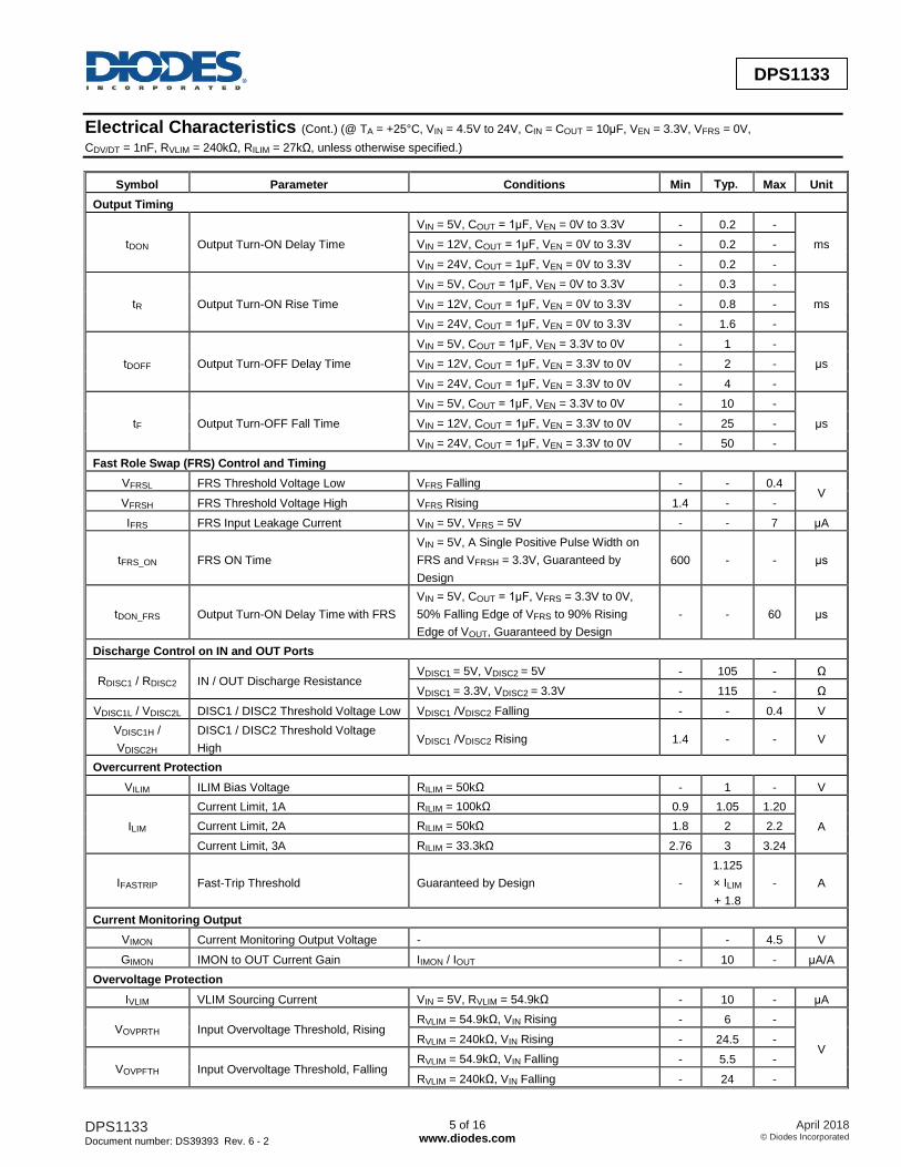
Electrical Characteristics (@ TA = +25°C, VIN = 4.5V to 24V, CIN = COUT = 10μF, VEN = 3.3V, VFRS = 0V, CDV/DT = 1nF,
RVLIM = 240kΩ, RILIM = 27kΩ, unless otherwise specified.)
Symbol Parameter Conditions Min Typ. Max Unit
Bias Supply
VREG Regulated Voltage
VIN = 5V - 4.9 -
V VIN = 12V - 5.1 -
VIN = 24V - 5.2 -
VUVLO VIN Undervoltage Lock-out Threshold VIN Rising 3.2 3.6 4.0 V
VUVHY VIN Undervoltage Lock-out Threshold
Hysteresis VIN Falling - 250 - mV
ISHDN Shut-down Current (Disabled)
VIN = 5V, VEN = 0V - - 5
μA VIN = 12V, VEN = 0V - - 15
VIN = 24V, VEN = 0V - - 25
IQ Quiescent Current (Enabled)
VIN = 5V, No Load - 1.2 1.6
mA VIN = 12V, No Load - 1.4 1.8
VIN = 24V, No Load - 1.9 2.3
MOSFET
RDS(ON) Switch ON Resistance
VIN = 5V - 29 36
mΩ VIN = 12V - 29 36
VIN = 24V - 30 36
ILKGSRC OUT Leakage Current in OFF State,
Sourcing VEN = 0V, VOUT = 0V - - 1 μA
ILKGSNK OUT Leakage Current in OFF State,
Sinking
VIN = 3.3V, VEN = 0V, VOUT = 5V - - 15
μA VIN = 3.3V, VEN = 0V, VOUT = 12V - - 25
VIN = 3.3V, VEN = 0V, VOUT = 24V - - 40
Enable Control
VENL EN Threshold Voltage Low VEN Falling - - 0.4 V
VENH EN Threshold Voltage High VEN Rising 1.4 - -
IEN EN Input Leakage Current VIN = 5V, VEN = 5V - - 5 μA
Output Ramping Control
IDV/DT DV/DT Sourcing Current VDV/DT = 0V - 1 - μA
GDV/DT DV/DT to OUT Gain ∆VOUT / ∆VDV/DT, Guaranteed by Design - 12 - V/V
DPS1133 Document number: DS39393 Rev. 6 - 2
5 of 16 www.diodes.com
April 2018 © Diodes Incorporated
DPS1133
Electrical Characteristics (Cont.) (@ TA = +25°C, VIN = 4.5V to 24V, CIN = COUT = 10μF, VEN = 3.3V, VFRS = 0V,
CDV/DT = 1nF, RVLIM = 240kΩ, RILIM = 27kΩ, unless otherwise specified.)
Symbol Parameter Conditions Min Typ. Max Unit
Output Timing
tDON Output Turn-ON Delay Time
VIN = 5V, COUT = 1μF, VEN = 0V to 3.3V - 0.2 -
ms VIN = 12V, COUT = 1μF, VEN = 0V to 3.3V - 0.2 -
VIN = 24V, COUT = 1μF, VEN = 0V to 3.3V - 0.2 -
tR Output Turn-ON Rise Time
VIN = 5V, COUT = 1μF, VEN = 0V to 3.3V - 0.3 -
ms VIN = 12V, COUT = 1μF, VEN = 0V to 3.3V - 0.8 -
VIN = 24V, COUT = 1μF, VEN = 0V to 3.3V - 1.6 -
tDOFF Output Turn-OFF Delay Time
VIN = 5V, COUT = 1μF, VEN = 3.3V to 0V - 1 -
μs VIN = 12V, COUT = 1μF, VEN = 3.3V to 0V - 2 -
VIN = 24V, COUT = 1μF, VEN = 3.3V to 0V - 4 -
tF Output Turn-OFF Fall Time
VIN = 5V, COUT = 1μF, VEN = 3.3V to 0V - 10 -
μs VIN = 12V, COUT = 1μF, VEN = 3.3V to 0V - 25 -
VIN = 24V, COUT = 1μF, VEN = 3.3V to 0V - 50 -
Fast Role Swap (FRS) Control and Timing
VFRSL FRS Threshold Voltage Low VFRS Falling - - 0.4 V
VFRSH FRS Threshold Voltage High VFRS Rising 1.4 - -
IFRS FRS Input Leakage Current VIN = 5V, VFRS = 5V - - 7 μA
tFRS_ON FRS ON Time
VIN = 5V, A Single Positive Pulse Width on
FRS and VFRSH = 3.3V, Guaranteed by
Design
600 - - μs
tDON_FRS Output Turn-ON Delay Time with FRS
VIN = 5V, COUT = 1μF, VFRS = 3.3V to 0V,
50% Falling Edge of VFRS to 90% Rising
Edge of VOUT, Guaranteed by Design
- - 60 μs
Discharge Control on IN and OUT Ports
RDISC1 / RDISC2 IN / OUT Discharge Resistance VDISC1 = 5V, VDISC2 = 5V - 105 - Ω
VDISC1 = 3.3V, VDISC2 = 3.3V - 115 - Ω
VDISC1L / VDISC2L DISC1 / DISC2 Threshold Voltage Low VDISC1 /VDISC2 Falling - - 0.4 V
VDISC1H /
VDISC2H
DISC1 / DISC2 Threshold Voltage
High VDISC1 /VDISC2 Rising 1.4 - - V
Overcurrent Protection
VILIM ILIM Bias Voltage RILIM = 50kΩ - 1 - V
ILIM
Current Limit, 1A RILIM = 100kΩ 0.9 1.05 1.20
A Current Limit, 2A RILIM = 50kΩ 1.8 2 2.2
Current Limit, 3A RILIM = 33.3kΩ 2.76 3 3.24
IFASTRIP Fast-Trip Threshold Guaranteed by Design -
1.125
× ILIM
+ 1.8
- A
Current Monitoring Output
VIMON Current Monitoring Output Voltage - - 4.5 V
GIMON IMON to OUT Current Gain IIMON / IOUT - 10 - μA/A
Overvoltage Protection
IVLIM VLIM Sourcing Current VIN = 5V, RVLIM = 54.9kΩ - 10 - μA
VOVPRTH Input Overvoltage Threshold, Rising RVLIM = 54.9kΩ, VIN Rising - 6 -
V RVLIM = 240kΩ, VIN Rising - 24.5 -
VOVPFTH Input Overvoltage Threshold, Falling RVLIM = 54.9kΩ, VIN Falling - 5.5 -
RVLIM = 240kΩ, VIN Falling - 24 -
DPS1133 Document number: DS39393 Rev. 6 - 2
6 of 16 www.diodes.com
April 2018 © Diodes Incorporated
DPS1133
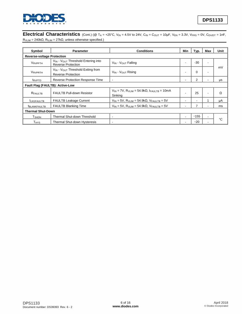
Electrical Characteristics (Cont.) (@ TA = +25°C, VIN = 4.5V to 24V, CIN = COUT = 10μF, VEN = 3.3V, VFRS = 0V, CDV/DT = 1nF,
RVLIM = 240kΩ, RILIM = 27kΩ, unless otherwise specified.)
Symbol Parameter Conditions Min Typ. Max Unit
Reverse-voltage Protection
VRVPFTH VIN - VOUT Threshold Entering into Reverse Protection
VIN - VOUT Falling - -30 -
mV
VRVPRTH VIN - VOUT Threshold Exiting from
Reverse Protection VIN - VOUT Rising - 0 -
tRVPTD Reverse Protection Response Time - - 2 - μs
Fault Flag (FAULTB): Active-Low
RFAULTB FAULTB Pull-down Resistor VIN = 7V, RVLIM = 54.9kΩ, IFAULTB = 10mA
Sinking - 25 - Ω
ILKGFAULTB FAULTB Leakage Current VIN = 5V, RVLIM = 54.9kΩ, VFAULTB = 5V - - 1 μA
tBLANKFAULTB FAULTB Blanking Time VIN = 5V, RVLIM = 54.9kΩ, VFAULTB = 5V - 7 - ms
Thermal Shut-Down
TSHDN Thermal Shut-down Threshold - - +155 - °C
THYS Thermal Shut-down Hysteresis - - +20 -
DPS1133 Document number: DS39393 Rev. 6 - 2
7 of 16 www.diodes.com
April 2018 © Diodes Incorporated
DPS1133
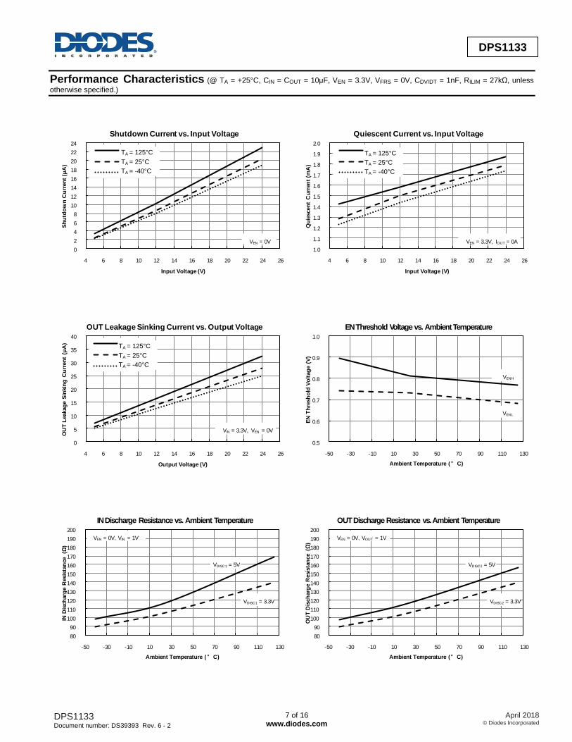
Performance Characteristics (@ TA = +25°C, CIN = COUT = 10μF, VEN = 3.3V, VFRS = 0V, CDV/DT = 1nF, RILIM = 27kΩ, unless
otherwise specified.)
0
2
4
6
8
10
12
14
16
18
20
22
24
4 6 8 10 12 14 16 18 20 22 24 26
Sh
utd
ow
n C
urr
en
t (μ
A)
Input Voltage (V)
Shutdown Current vs. Input Voltage
TA = 125 C
TA = 25 C
TA = -40 C
VEN = 0V
1.0
1.1
1.2
1.3
1.4
1.5
1.6
1.7
1.8
1.9
2.0
4 6 8 10 12 14 16 18 20 22 24 26
Qu
iescen
t C
urr
en
t (m
A)
Input Voltage (V)
Quiescent Current vs. Input Voltage
TA = 125 C
TA = 25 C
TA = -40 C
VEN = 3.3V, IOUT = 0A
0
5
10
15
20
25
30
35
40
4 6 8 10 12 14 16 18 20 22 24 26
OU
T L
eakag
e S
inkin
g C
urr
en
t (μ
A)
Output Voltage (V)
OUT Leakage Sinking Current vs. Output Voltage
TA = 125 C
TA = 25 C
TA = -40 C
VIN = 3.3V, VEN = 0V
0.5
0.6
0.7
0.8
0.9
1.0
-50 -30 -10 10 30 50 70 90 110 130
EN
Th
resh
old
Vo
ltag
e (
V)
Ambient Temperature (°C)
EN Threshold Voltage vs. Ambient Temperature
VENH
VENL
80
90
100
110
120
130
140
150
160
170
180
190
200
-50 -30 -10 10 30 50 70 90 110 130
IN D
isch
arg
e R
esis
tan
ce
(Ω)
Ambient Temperature (°C)
IN Discharge Resistance vs. Ambient Temperature
VEN = 0V, VIN = 1V
VDISC1 = 5V
VDISC1 = 3.3V
80
90
100
110
120
130
140
150
160
170
180
190
200
-50 -30 -10 10 30 50 70 90 110 130
OU
T D
isch
arg
e R
esis
tan
ce (Ω
)
Ambient Temperature (°C)
OUT Discharge Resistance vs. Ambient Temperature
VEN = 0V, VOUT = 1V
VDISC2 = 5V
VDISC2 = 3.3V
TA = 125°C
TA = 25°C
TA = -40°C
TA = 125°C
TA = 25°C
TA = -40°C
TA = 125°C
TA = 25°C
TA = -40°C
DPS1133 Document number: DS39393 Rev. 6 - 2
8 of 16 www.diodes.com
April 2018 © Diodes Incorporated
DPS1133
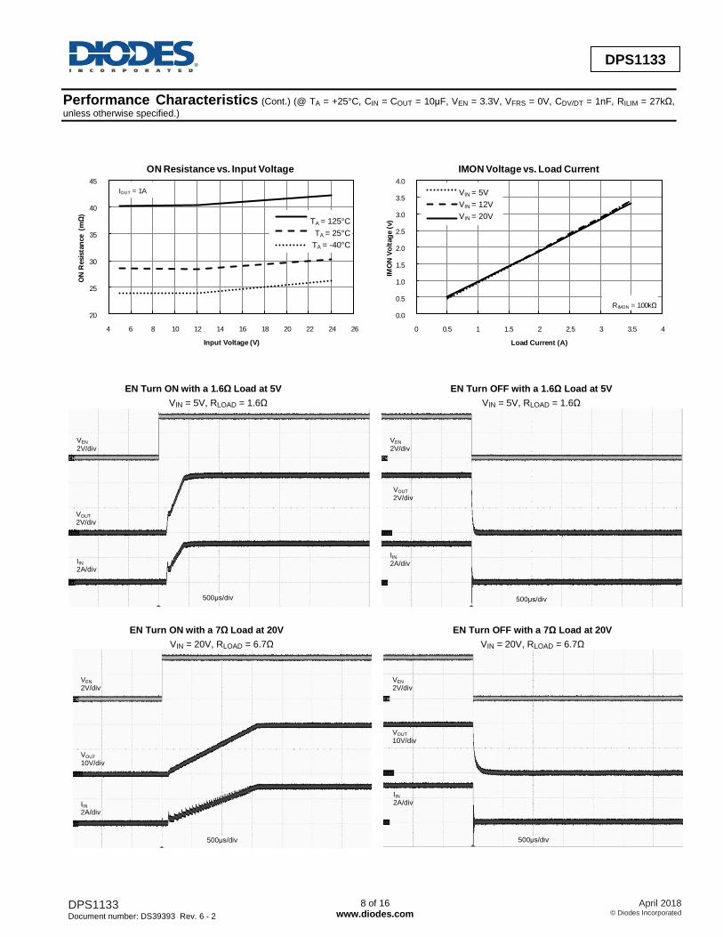
Performance Characteristics (Cont.) (@ TA = +25°C, CIN = COUT = 10μF, VEN = 3.3V, VFRS = 0V, CDV/DT = 1nF, RILIM = 27kΩ,
unless otherwise specified.)
20
25
30
35
40
45
4 6 8 10 12 14 16 18 20 22 24 26
ON
Resis
tan
ce (m
Ω)
Input Voltage (V)
ON Resistance vs. Input Voltage
TA = 125 C
TA = 25 C
TA = -40 C
IOUT = 1A
0.0
0.5
1.0
1.5
2.0
2.5
3.0
3.5
4.0
0 0.5 1 1.5 2 2.5 3 3.5 4
IMO
N V
olt
ag
e (
v)
Load Current (A)
IMON Voltage vs. Load Current
VIN = 5V
VIN = 12V
VIN = 20V
RIMON = 100kΩ
EN Turn ON with a 1.6Ω Load at 5V EN Turn OFF with a 1.6Ω Load at 5V
VIN = 5V, RLOAD = 1.6Ω
VIN = 5V, RLOAD = 1.6Ω
EN Turn ON with a 7Ω Load at 20V EN Turn OFF with a 7Ω Load at 20V
VIN = 20V, RLOAD = 6.7Ω
VIN = 20V, RLOAD = 6.7Ω
500μs/div
VEN 2V/div
VOUT 2V/div
IIN 2A/div
VEN 2V/div
VOUT 2V/div
IIN 2A/div
VEN 2V/div
VOUT 10V/div
IIN 2A/div
500μs/div
VEN 2V/div
VOUT 10V/div
IIN 2A/div
500μs/div
500μs/div
TA = 125°C
TA = 25°C
TA = -40°C
VIN = 5V
VIN = 12V
VIN = 20V
DPS1133 Document number: DS39393 Rev. 6 - 2
9 of 16 www.diodes.com
April 2018 © Diodes Incorporated
DPS1133
Performance Characteristics (Cont.) (@ TA = +25°C, CIN = COUT = 10μF, VEN = 3.3V, VFRS = 0V, CDV/DT = 1nF, RILIM = 27kΩ,
unless otherwise specified.)
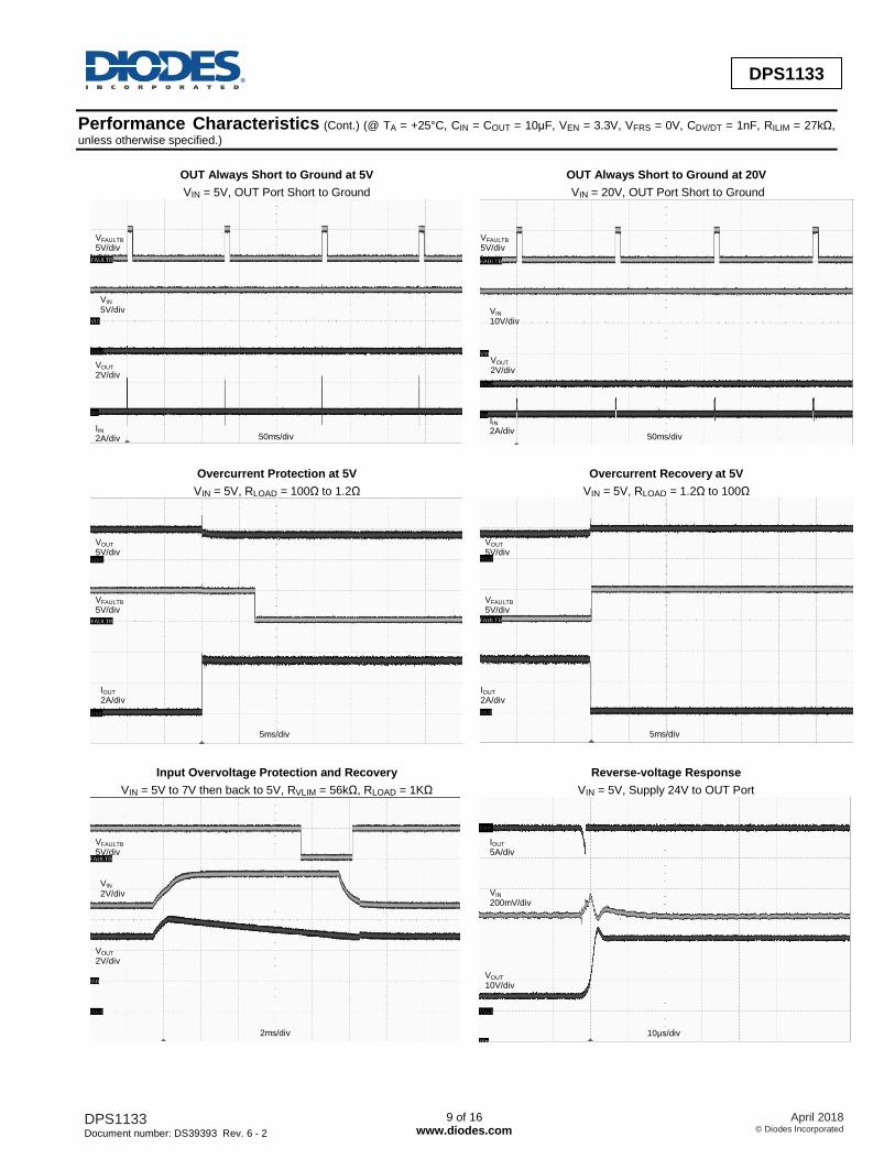
OUT Always Short to Ground at 5V OUT Always Short to Ground at 20V
VIN = 5V, OUT Port Short to Ground
VIN = 20V, OUT Port Short to Ground
Overcurrent Protection at 5V Overcurrent Recovery at 5V
VIN = 5V, RLOAD = 100Ω to 1.2Ω
VIN = 5V, RLOAD = 1.2Ω to 100Ω
Input Overvoltage Protection and Recovery Reverse-voltage Response
VIN = 5V to 7V then back to 5V, RVLIM = 56kΩ, RLOAD = 1KΩ
VIN = 5V, Supply 24V to OUT Port
VIN 5V/div
VFAULTB 5V/div
VOUT 2V/div
IIN 2A/div
VOUT 2V/div
VIN 10V/div
VFAULTB 5V/div
50ms/div 50ms/div
IIN 2A/div
VFAULTB 5V/div
VOUT 5V/div
IOUT 2A/div
IOUT 2A/div
VOUT 5V/div
VFAULTB 5V/div
5ms/div 5ms/div
VOUT 2V/div
VFAULTB 5V/div
VIN 2V/div
2ms/div
VIN
200mV/div
VOUT 10V/div
IOUT 5A/div
10μs/div
DPS1133 Document number: DS39393 Rev. 6 - 2
10 of 16 www.diodes.com
April 2018 © Diodes Incorporated
DPS1133
Application Information
General Description
The DPS1133 is a 1-channel power switch designed to meet the input and output voltage/current requirement which are common with many hot-
pluggable serial interfaces found in the computing and consumer electronics equipment. For example, DPS1133 is compatible to the USB Power
Delivery Specification Release 3.0, V1.0a and many popular USB Type-CTM
applications.
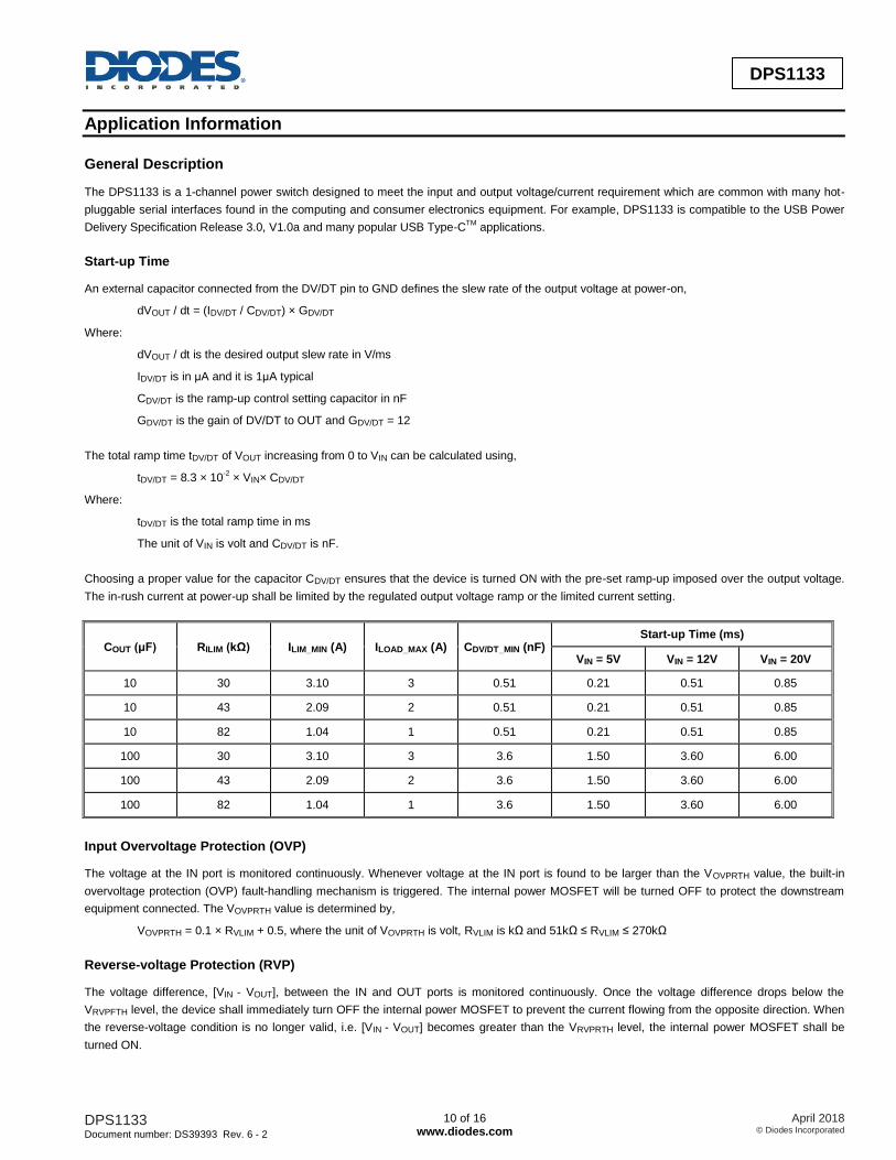
Start-up Time
An external capacitor connected from the DV/DT pin to GND defines the slew rate of the output voltage at power-on,
dVOUT / dt = (IDV/DT / CDV/DT) × GDV/DT
Where:
dVOUT / dt is the desired output slew rate in V/ms
IDV/DT is in μA and it is 1μA typical
CDV/DT is the ramp-up control setting capacitor in nF
GDV/DT is the gain of DV/DT to OUT and GDV/DT = 12
The total ramp time tDV/DT of VOUT increasing from 0 to VIN can be calculated using,
tDV/DT = 8.3 × 10⁻² × VIN× CDV/DT
Where:
tDV/DT is the total ramp time in ms
The unit of VIN is volt and CDV/DT is nF.
Choosing a proper value for the capacitor CDV/DT ensures that the device is turned ON with the pre-set ramp-up imposed over the output voltage.
The in-rush current at power-up shall be limited by the regulated output voltage ramp or the limited current setting.
COUT (μF) RILIM (kΩ) ILIM_MIN (A) ILOAD_MAX (A) CDV/DT_MIN (nF) Start-up Time (ms)
VIN = 5V VIN = 12V VIN = 20V
10 30 3.10 3 0.51 0.21 0.51 0.85
10 43 2.09 2 0.51 0.21 0.51 0.85
10 82 1.04 1 0.51 0.21 0.51 0.85
100 30 3.10 3 3.6 1.50 3.60 6.00
100 43 2.09 2 3.6 1.50 3.60 6.00
100 82 1.04 1 3.6 1.50 3.60 6.00
Input Overvoltage Protection (OVP)
The voltage at the IN port is monitored continuously. Whenever voltage at the IN port is found to be larger than the VOVPRTH value, the built-in
overvoltage protection (OVP) fault-handling mechanism is triggered. The internal power MOSFET will be turned OFF to protect the downstream
equipment connected. The VOVPRTH value is determined by,
VOVPRTH = 0.1 × RVLIM + 0.5, where the unit of VOVPRTH is volt, RVLIM is kΩ and 51kΩ ≤ RVLIM ≤ 270kΩ
Reverse-voltage Protection (RVP)
The voltage difference, [VIN - VOUT], between the IN and OUT ports is monitored continuously. Once the voltage difference drops below the
VRVPFTH level, the device shall immediately turn OFF the internal power MOSFET to prevent the current flowing from the opposite direction. When
the reverse-voltage condition is no longer valid, i.e. [VIN - VOUT] becomes greater than the VRVPRTH level, the internal power MOSFET shall be
turned ON.
DPS1133 Document number: DS39393 Rev. 6 - 2
11 of 16 www.diodes.com
April 2018 © Diodes Incorporated
DPS1133
Application Information (Cont.)
Overtemperature Protection (OTP)
During overload conditions, the output voltage would drop with the limited current ILIM. It will result in the increasing junction temperature TJ with
the increased power consumption on device. When TJ reaches to the thermal shutdown threshold TSHDN, the internal power MOSFET would be
turned OFF. The internal MOSFET would be turned ON again once the condition [TJ < (TSHDN - THYS)] occurs.
Overcurrent Protection (OCP)
The output current is being monitored continuously. Whenever the output current IOUT is found to be larger than the ILIM value over 2μs, the
embedded overcurrent protection (OCP) fault-handling mechanism is triggered. This shall result in the output current being clamped at the ILIM
value at hundreds of microseconds later, and voltage dropping at OUT port. The ILIM value is set by RILIM,
ILIM = 100 / RILIM, where the unit of ILIM is ampere, RILIM is kΩ and 27kΩ ≤ RILIM ≤ 200kΩ
RILIM (kΩ) ILIM (A)
Min Typ Max
200 0.50 0.55 0.7
100 0.90 1.05 1.20
66.7 1.35 1.50 1.65
50 1.80 2.00 2.20
40 2.25 2.50 2.75
33.3 2.76 3.00 3.24
28.6 3.22 3.50 3.78
Short-circuit Protection (SCP)
There are two behaviors to protect device under short-circuit conditions. One is fast trip current detection. When the output current exceeds the
fast-trip threshold IFASTRIP, the device will switch OFF the internal MOSFET,
IFASTRIP = 1.125 × ILIM + 1.8, where the unit of IFASTRIP and ILIM is ampere
Another is low output voltage detection. During heavy overload or short circuit conditions, the output current is limited to ILIM and the output voltage
would drop quickly. When the output voltage drop is exceeded the capability of MOSFET, the power switch will be turned OFF. The device is
operating in auto-retry mode and the cycle time is around 128ms.
Adjustable Current Monitoring Output (IMON)
A 100pF capacitor and a resistor RIMON connected in parallel between the IMON pin and GND will generate an average current monitor output
voltage VIMON, which is proportional to the load current flowing through the device,
VIMON = 10-3 × GIMON × RIMON × IOUT,
Where:
GIMON is the ratio of the IMON to the load current in μA/A and GIMON = 10
The unit of VIMON is volt, RIMON is kΩ and IOUT is ampere
The resistor RIMON should be chosen to ensure that the voltage at the IMON pin is less than 4.5V under the maximum load current I ILIM. For
example, if RIMON is selected as 100kΩ, there will be a 1V output on IMON pin at 1A load, and VIMON = 3V at 3A load. Connecting this IMON pin to
an ADC could help to monitor the current information of a system.
Fault Response
An external pull-up resistor is required. The device generates a warning flag whenever one of the following fault conditions becomes valid: input
overvoltage, reverse-voltage, overtemperature, short-circuit, overcurrent, ILIM pin short to ground. After a de-glitch time-out of 7ms, the low-active
FAULTB signal shall be asserted. The FAULTB signal shall remain at ‘low’ and the internal power MOSFET remains OFF until the device exits
from the exception status.
DPS1133 Document number: DS39393 Rev. 6 - 2
12 of 16 www.diodes.com
April 2018 © Diodes Incorporated
DPS1133
Application Information (Cont.)
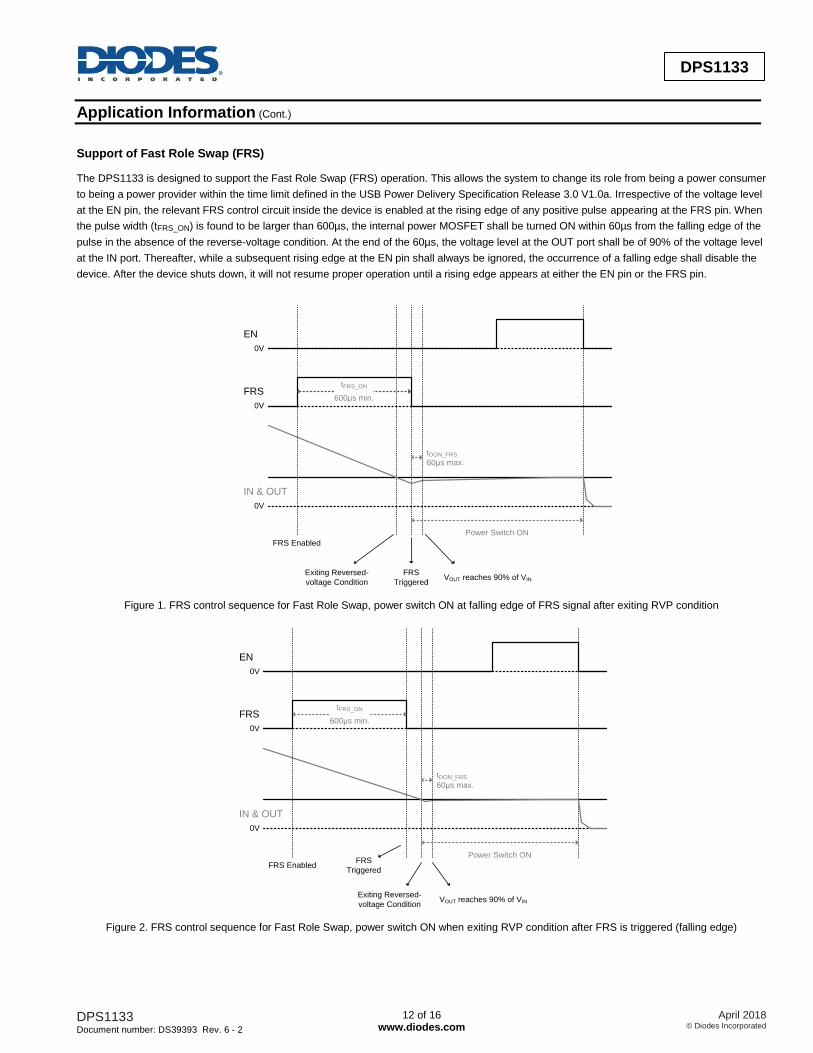
Support of Fast Role Swap (FRS)
The DPS1133 is designed to support the Fast Role Swap (FRS) operation. This allows the system to change its role from being a power consumer
to being a power provider within the time limit defined in the USB Power Delivery Specification Release 3.0 V1.0a. Irrespective of the voltage level
at the EN pin, the relevant FRS control circuit inside the device is enabled at the rising edge of any positive pulse appearing at the FRS pin. When
the pulse width (tFRS_ON) is found to be larger than 600µs, the internal power MOSFET shall be turned ON within 60µs from the falling edge of the
pulse in the absence of the reverse-voltage condition. At the end of the 60µs, the voltage level at the OUT port shall be of 90% of the voltage level
at the IN port. Thereafter, while a subsequent rising edge at the EN pin shall always be ignored, the occurrence of a falling edge shall disable the
device. After the device shuts down, it will not resume proper operation until a rising edge appears at either the EN pin or the FRS pin.
FRS
EN
IN & OUT
0V
0V
0V
FRS Enabled
FRS
Triggered
Exiting Reversed-
voltage ConditionVOUT reaches 90% of VIN
tDON_FRS
60μs max.
Power Switch ON
tFRS_ON
600μs min.
Figure 1. FRS control sequence for Fast Role Swap, power switch ON at falling edge of FRS signal after exiting RVP condition
FRS
EN
IN & OUT
0V
0V
0V
FRS EnabledFRS
Triggered
Exiting Reversed-
voltage ConditionVOUT reaches 90% of VIN
tDON_FRS
60μs max.
Power Switch ON
tFRS_ON
600μs min.
Figure 2. FRS control sequence for Fast Role Swap, power switch ON when exiting RVP condition after FRS is triggered (falling edge)
DPS1133 Document number: DS39393 Rev. 6 - 2
13 of 16 www.diodes.com
April 2018 © Diodes Incorporated
DPS1133
Application Information (Cont.)
Discharge Function
To facilitate the various applications envisioned by the system designers, the input or output port can be discharged via two external controls:
DISC1, DISC2. The internal discharge resistor at each port is approximately 100Ω. The discharge paths are OFF by default with an internal 1MΩ
pull-down resistor between DISC1 (or DISC2) and GND. The settings are shown in the table below.
DISC1 DISC2 Description
0 0 Discharge function disabled
0 1 OUT port is being discharged until the pin DISC2 is pulled ‘low’
1 0 IN port is being discharged until the pin DISC1 is pulled ‘low’
1 1 Both IN and OUT ports are discharged simultaneously
Schottky Diode for Protection of Current Surge
When a cable is hot plugged in/out of the USB-C connector behind which the OUT port of the DPS1133 is connected, a large ground current could
be seen at the OUT port of the DPS1133. When the far end of a connected cable is short to ground for whatever reason, the OUT port of the
DPS1133 could also see a large ground current. With the Schottky diode, SBR3U40P1, populated as close as possible to the USB-C connector,
no ground current can go through the DPS1133 to cause false operation.
PCB Layout Consideration
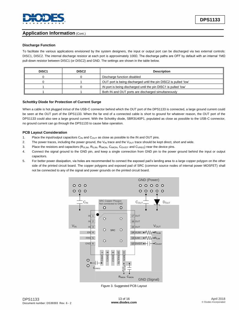
1. Place the input/output capacitors CIN and COUT as close as possible to the IN and OUT pins.
2. The power traces, including the power ground, the VIN trace and the VOUT trace should be kept direct, short and wide.
3. Place the resistors and capacitors (RVLIM, RILIM, RIMON, CIMON, CDV/DT and CVREG) near the device pins.
4. Connect the signal ground to the GND pin, and keep a single connection from GND pin to the power ground behind the input or output
capacitors.
5. For better power dissipation, via holes are recommended to connect the exposed pad’s landing area to a large copper polygon on the other
side of the printed circuit board. The copper polygons and exposed pad of SRC (common source nodes of internal power MOSFET) shall
not be connected to any of the signal and power grounds on the printed circuit board.
GND (Power)
RVLIM
CIN COUT
RILIM
CDV/DT
CVREG
VOUTVIN
2
1
3
4
5
6
SRC
16
17
15
14
13
12
87 9 10
11
DIS
C1
IN
IN
IN
EN
FRS
GND
VR
EG
DIS
C2
FA
UL
TB
OUT
OUT
OUT
VLIM
ILIM
DV/DT
SRC Copper Ploygon
Not connected to GND
GND (Signal)RIMON
IMO
N
DOUT
CIMON
Figure 3. Suggested PCB Layout
DPS1133 Document number: DS39393 Rev. 6 - 2
14 of 16 www.diodes.com
April 2018 © Diodes Incorporated
DPS1133
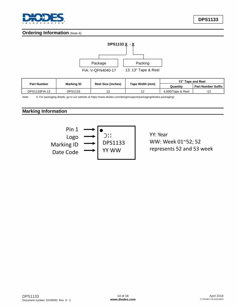
Ordering Information (Note 6)
DPS1133 X - X
PackingPackage
13: 13" Tape & ReelFIA: V-QFN4040-17
Part Number Marking ID Reel Size (inches) Tape Width (mm) 13” Tape and Reel
Quantity Part Number Suffix
DPS1133FIA-13 DPS1133 13 12 4,000/Tape & Reel -13
Note: 6. For packaging details, go to our website at https://www.diodes.com/design/support/packaging/diodes-packaging/.
Marking Information
Pin 1
Logo
Marking ID
Date Code
DPS1133
YY WW
YY: Year
WW: Week 01~52; 52 represents 52 and 53 week
DPS1133 Document number: DS39393 Rev. 6 - 2
15 of 16 www.diodes.com
April 2018 © Diodes Incorporated
DPS1133
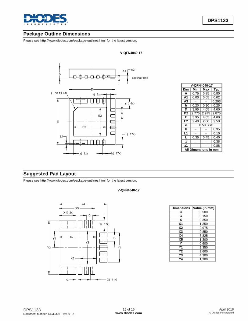
Package Outline Dimensions
Please see http://www.diodes.com/package-outlines.html for the latest version.
V-QFN4040-17
D
D2
E
b(17x)
L(17x)
E2
AA1 A3
(Pin #1 ID)
Seating Plane
z(2x)
e
z1(4x)
k(3x)
L1
V-QFN4040-17
Dim Min Max Typ
A 0.75 0.85 0.80
A1 0.00 0.05 0.02
A3 0.203
b 0.20 0.30 0.25
D 3.95 4.05 4.00
D2 2.775 2.975 2.875
E 3.95 4.05 4.00
E2 2.40 2.60 2.50
e 0.50 BSC
k 0.35
L1 0.10
L 0.35 0.45 0.40
z 0.38
z1 0.88
All Dimensions in mm
Suggested Pad Layout
Please see http://www.diodes.com/package-outlines.html for the latest version.
V-QFN4040-17
X3
C
X2
Y2
Y1
C
X(11x)
Y3
X1(2x)
Y(17x)
X5
X4
Y4
G
Dimensions Value (in mm)
C 0.500
G 0.150
X 0.350
X1 1.350
X2 2.975
X3 2.850
X4 3.825
X5 1.300
Y 0.600
Y1 2.350
Y2 2.600
Y3 4.300
Y4 1.300
DPS1133 Document number: DS39393 Rev. 6 - 2
16 of 16 www.diodes.com
April 2018 © Diodes Incorporated
DPS1133
IMPORTANT NOTICE DIODES INCORPORATED MAKES NO WARRANTY OF ANY KIND, EXPRESS OR IMPLIED, WITH REGARDS TO THIS DOCUMENT, INCLUDING, BUT NOT LIMITED TO, THE IMPLIED WARRANTIES OF MERCHANTABILITY AND FITNESS FOR A PARTICULAR PURPOSE (AND THEIR EQUIVALENTS UNDER THE LAWS OF ANY JURISDICTION). Diodes Incorporated and its subsidiaries reserve the right to make modifications, enhancements, improvements, corrections or other changes without further notice to this document and any product described herein. Diodes Incorporated does not assume any liability arising out of the application or use of this document or any product described herein; neither does Diodes Incorporated convey any license under its patent or trademark rights, nor the rights of others. Any Customer or user of this document or products described herein in such applications shall assume all risks of such use and will agree to hold Diodes Incorporated and all the companies whose products are represented on Diodes Incorporated website, harmless against all damages. Diodes Incorporated does not warrant or accept any liability whatsoever in respect of any products purchased through unauthorized sales channel. Should Customers purchase or use Diodes Incorporated products for any unintended or unauthorized application, Customers shall indemnify and hold Diodes Incorporated and its representatives harmless against all claims, damages, expenses, and attorney fees arising out of, directly or indirectly, any claim of personal injury or death associated with such unintended or unauthorized application. Products described herein may be covered by one or more United States, international or foreign patents pending. Product names and markings noted herein may also be covered by one or more United States, international or foreign trademarks. This document is written in English but may be translated into multiple languages for reference. Only the English version of this document is the final and determinative format released by Diodes Incorporated.
LIFE SUPPORT Diodes Incorporated products are specifically not authorized for use as critical components in life support devices or systems without the express written approval of the Chief Executive Officer of Diodes Incorporated. As used herein: A. Life support devices or systems are devices or systems which: 1. are intended to implant into the body, or
2. support or sustain life and whose failure to perform when properly used in accordance with instructions for use provided in the labeling can be reasonably expected to result in significant injury to the user.
B. A critical component is any component in a life support device or system whose failure to perform can be reasonably expected to cause the failure of the life support device or to affect its safety or effectiveness. Customers represent that they have all necessary expertise in the safety and regulatory ramifications of their life support devices or systems, and acknowledge and agree that they are solely responsible for all legal, regulatory and safety-related requirements concerning their products and any use of Diodes Incorporated products in such safety-critical, life support devices or systems, notwithstanding any devices- or systems-related information or support that may be provided by Diodes Incorporated. Further, Customers must fully indemnify Diodes Incorporated and its representatives against any damages arising out of the use of Diodes Incorporated products in such safety-critical, life support devices or systems. Copyright © 2018, Diodes Incorporated www.diodes.com


![Untitled-6 [ilim-lib.narod.ru]ilim-lib.narod.ru/Chernyh_noty/Letuchaya_kosh.pdf · l. Komvxa 110KOH Mb1LL1atv[ He AaBana Cepb1M xwrb11aM qepnaKa rt0ABaJ1a. ee HaKä3aTb, eil r10Ka3aTb](https://img.pdfslide.us/doc/110x75/603876cd66cd4d56a07c1839/untitled-6-ilim-libnarodruilim-libnarodruchernyhnotyletuchayakoshpdf.jpg)