Embed Size (px)
Citation preview
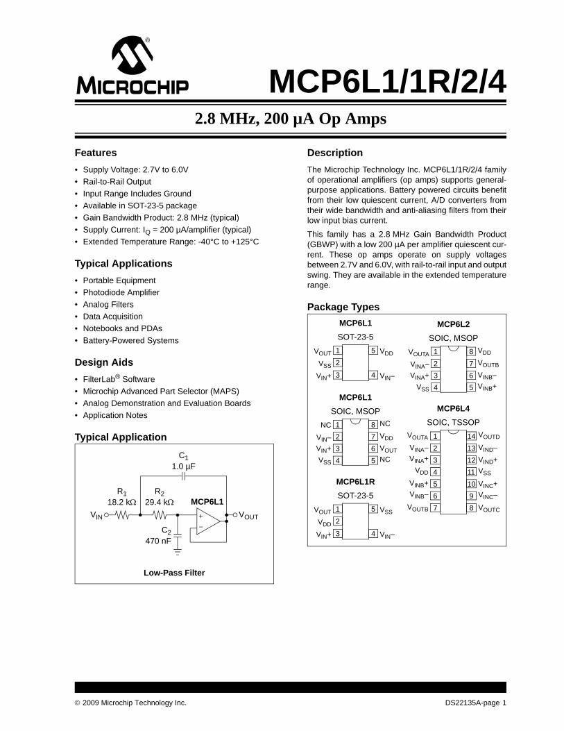
MCP6L1/1R/2/42.8 MHz, 200 µA Op Amps
Features• Supply Voltage: 2.7V to 6.0V• Rail-to-Rail Output• Input Range Includes Ground• Available in SOT-23-5 package• Gain Bandwidth Product: 2.8 MHz (typical)• Supply Current: IQ = 200 µA/amplifier (typical)• Extended Temperature Range: -40°C to +125°C
Typical Applications• Portable Equipment• Photodiode Amplifier• Analog Filters• Data Acquisition• Notebooks and PDAs• Battery-Powered Systems
Design Aids• FilterLab® Software• Microchip Advanced Part Selector (MAPS)• Analog Demonstration and Evaluation Boards• Application Notes
Typical Application
DescriptionThe Microchip Technology Inc. MCP6L1/1R/2/4 familyof operational amplifiers (op amps) supports general-purpose applications. Battery powered circuits benefitfrom their low quiescent current, A/D converters fromtheir wide bandwidth and anti-aliasing filters from theirlow input bias current.
This family has a 2.8 MHz Gain Bandwidth Product(GBWP) with a low 200 µA per amplifier quiescent cur-rent. These op amps operate on supply voltagesbetween 2.7V and 6.0V, with rail-to-rail input and outputswing. They are available in the extended temperaturerange.
Package Types
Low-Pass Filter
R1
VIN VOUT
R218.2 kΩ 29.4 kΩ MCP6L1
C2470 nF
C11.0 µF
MCP6L1SOT-23-5
MCP6L2SOIC, MSOP
VIN+
VSS
VIN–
1
2
3
5
4
VDDVOUT
VINA+VINA–
VSS
1234
8765
VOUTA VDD
VOUTB
VINB–VINB+
MCP6L4SOIC, TSSOP
VINA+VINA–
VDD
1234
14131211
VOUTA VOUTD
VIND–VIND+VSS
VINB+ 5 10 VINC+MCP6L1RSOT-23-5
VIN+
VDD
VIN–
1
2
3
5
4
VSSVOUT
VINB– 6 9 VINC–
VOUTB 7 8 VOUTC
MCP6L1SOIC, MSOP
VIN+VIN–
VSS
1234
8765
NC NC
VDD
VOUTNC
© 2009 Microchip Technology Inc. DS22135A-page 1

MCP6L1/1R/2/4
NOTES:DS22135A-page 2 © 2009 Microchip Technology Inc.
MCP6L1/1R/2/4
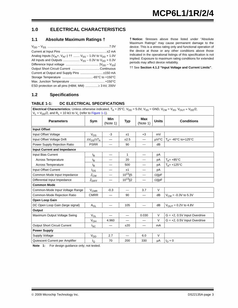
1.0 ELECTRICAL CHARACTERISTICS
1.1 Absolute Maximum Ratings †VDD – VSS .......................................................................7.0VCurrent at Input Pins ....................................................±2 mAAnalog Inputs (VIN+, VIN–) †† ....... VSS – 1.0V to VDD + 1.0VAll Inputs and Outputs ................... VSS – 0.3V to VDD + 0.3VDifference Input voltage ...................................... |VDD – VSS|Output Short Circuit Current ................................ContinuousCurrent at Output and Supply Pins ..........................±150 mAStorage Temperature ...................................-65°C to +150°CMax. Junction Temperature ........................................ +150°CESD protection on all pins (HBM, MM) ................≥ 3 kV, 200V
† Notice: Stresses above those listed under “AbsoluteMaximum Ratings” may cause permanent damage to thedevice. This is a stress rating only and functional operation ofthe device at those or any other conditions above thoseindicated in the operational listings of this specification is notimplied. Exposure to maximum rating conditions for extendedperiods may affect device reliability.†† See Section 4.1.2 “Input Voltage and Current Limits”.
1.2 Specifications
TABLE 1-1: DC ELECTRICAL SPECIFICATIONSElectrical Characteristics: Unless otherwise indicated, TA = 25°C, VDD = 5.0V, VSS = GND, VCM = VSS, VOUT ≈ VDD/2, VL = VDD/2, and RL = 10 kΩ to VL (refer to Figure 1-1).
Parameters Sym Min(Note 1) Typ Max
(Note 1) Units Conditions
Input OffsetInput Offset Voltage VOS -3 ±1 +3 mVInput Offset Voltage Drift ΔVOS/ΔTA — ±2.5 — µV/°C TA= -40°C to+125°CPower Supply Rejection Ratio PSRR — 90 — dBInput Current and ImpedanceInput Bias Current IB — 1 — pA
Across Temperature IB — 20 — pA TA= +85°CAcross Temperature IB — 500 — pA TA= +125°C
Input Offset Current IOS — ±1 — pACommon Mode Input Impedance ZCM — 1013||5 — Ω||pFDifferential Input Impedance ZDIFF — 1013||2 — Ω||pFCommon ModeCommon-Mode Input Voltage Range VCMR -0.3 — 3.7 VCommon-Mode Rejection Ratio CMRR — 90 — dB VCM = -0.3V to 5.3VOpen Loop GainDC Open Loop Gain (large signal) AOL — 105 — dB VOUT = 0.2V to 4.8VOutputMaximum Output Voltage Swing VOL — — 0.030 V G = +2, 0.5V Input Overdrive
VOH 4.960 — — V G = +2, 0.5V Input OverdriveOutput Short Circuit Current ISC — ±20 — mAPower SupplySupply Voltage VDD 2.7 — 6.0 VQuiescent Current per Amplifier IQ 70 200 330 µA IO = 0Note 1: For design guidance only; not tested.
© 2009 Microchip Technology Inc. DS22135A-page 3
MCP6L1/1R/2/4
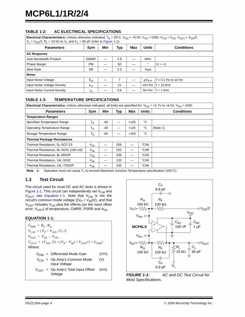
1.3 Test CircuitThe circuit used for most DC and AC tests is shown inFigure 1-1. This circuit can independently set VCM andVOUT; see Equation 1-1. Note that VCM is not thecircuit’s common mode voltage ((VP + VM)/2), and thatVOST includes VOS plus the effects (on the input offseterror, VOST) of temperature, CMRR, PSRR and AOL.
EQUATION 1-1:
FIGURE 1-1: AC and DC Test Circuit for Most Specifications.
TABLE 1-2: AC ELECTRICAL SPECIFICATIONSElectrical Characteristics: Unless otherwise indicated, TA = 25°C, VDD = +5.0V, VSS = GND, VCM = VSS, VOUT ≈ VDD/2, VL = VDD/2, RL = 10 kΩ to VL and CL = 60 pF (refer to Figure 1-1).
Parameters Sym Min Typ Max Units ConditionsAC ResponseGain Bandwidth Product GBWP — 2.8 — MHzPhase Margin PM — 50 — ° G = +1Slew Rate SR — 2.3 — V/µsNoiseInput Noise Voltage Eni — 7 — µVP-P f = 0.1 Hz to 10 HzInput Noise Voltage Density eni — 21 — nV/√Hz f = 10 kHzInput Noise Current Density ini — 0.6 — fA/√Hz f = 1 kHz
TABLE 1-3: TEMPERATURE SPECIFICATIONSElectrical Characteristics: Unless otherwise indicated, all limits are specified for: VDD = +2.7V to +6.0V, VSS = GND.
Parameters Sym Min Typ Max Units ConditionsTemperature RangesSpecified Temperature Range TA -40 — +125 °C
Operating Temperature Range TA -40 — +125 °C (Note 1)
Storage Temperature Range TA -65 — +150 °C
Thermal Package ResistancesThermal Resistance, 5L-SOT-23 θJA — 256 — °C/WThermal Resistance, 8L-SOIC (150 mil) θJA — 163 — °C/WThermal Resistance, 8L-MSOP θJA — 206 — °C/WThermal Resistance, 14L-SOIC θJA — 120 — °C/WThermal Resistance, 14L-TSSOP θJA — 100 — °C/WNote 1: Operation must not cause TJ to exceed Maximum Junction Temperature specification (150°C).
GDM RF RG⁄=VCM VP VDD 2⁄+( ) 2⁄=
VOUT VDD 2⁄( ) VP VM–( ) VOST 1 GDM+( )+ +=Where:
GDM = Differential Mode Gain (V/V)VCM = Op Amp’s Common Mode
Input Voltage(V)
VOST = Op Amp’s Total Input OffsetVoltage
(mV)
VOST VIN– VIN+–=
VDD
MCP6LX
RG RF
VOUTVM
CB2
CLRL
VL
CB1
100 kΩ100 kΩ
RG RF
VDD/2VP
100 kΩ100 kΩ
60 pF10 kΩ
1 µF100 nF
VIN–
VIN+
CF6.8 pF
CF6.8 pF
DS22135A-page 4 © 2009 Microchip Technology Inc.
MCP6L1/1R/2/4
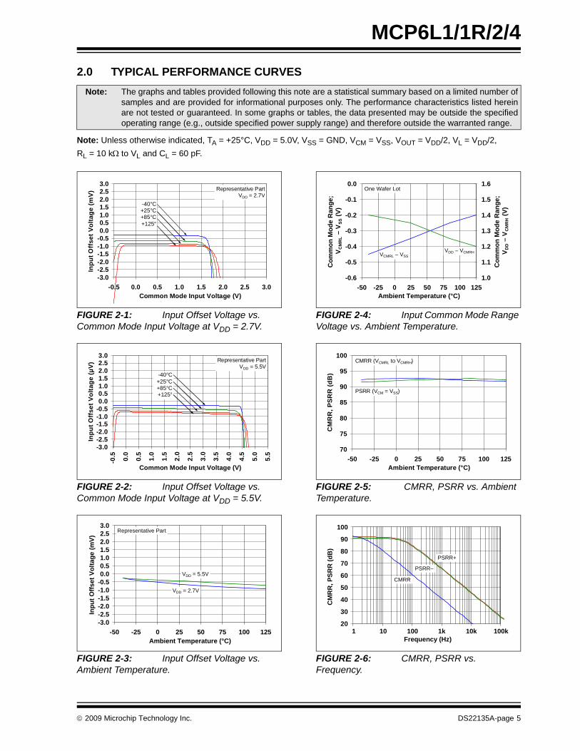
2.0 TYPICAL PERFORMANCE CURVES
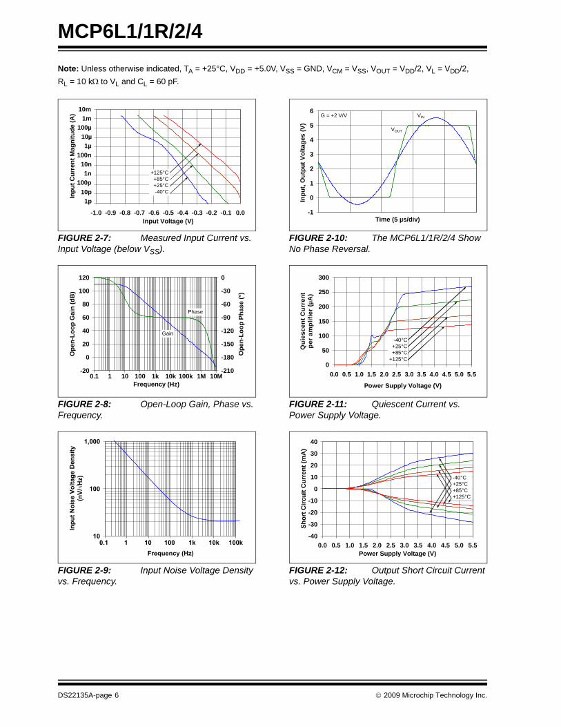
Note: Unless otherwise indicated, TA = +25°C, VDD = 5.0V, VSS = GND, VCM = VSS, VOUT = VDD/2, VL = VDD/2, RL = 10 kΩ to VL and CL = 60 pF.
FIGURE 2-1: Input Offset Voltage vs. Common Mode Input Voltage at VDD = 2.7V.
FIGURE 2-2: Input Offset Voltage vs. Common Mode Input Voltage at VDD = 5.5V.
FIGURE 2-3: Input Offset Voltage vs. Ambient Temperature.
FIGURE 2-4: Input Common Mode Range Voltage vs. Ambient Temperature.
FIGURE 2-5: CMRR, PSRR vs. Ambient Temperature.
FIGURE 2-6: CMRR, PSRR vs. Frequency.
Note: The graphs and tables provided following this note are a statistical summary based on a limited number ofsamples and are provided for informational purposes only. The performance characteristics listed hereinare not tested or guaranteed. In some graphs or tables, the data presented may be outside the specifiedoperating range (e.g., outside specified power supply range) and therefore outside the warranted range.
-3.0-2.5-2.0-1.5-1.0-0.50.00.51.01.52.02.53.0
-0.5 0.0 0.5 1.0 1.5 2.0 2.5 3.0Common Mode Input Voltage (V)
Inpu
t Off
set V
olta
ge (m
V)
Representative PartVDD = 2.7V
-40°C+25°C+85°C+125°
C
-3.0-2.5-2.0-1.5-1.0-0.50.00.51.01.52.02.53.0
-0.5 0.0
0.5
1.0
1.5
2.0
2.5
3.0
3.5
4.0
4.5
5.0
5.5
Common Mode Input Voltage (V)
Inpu
t Off
set V
olta
ge (µ
V)
Representative PartVDD = 5.5V
-40°C+25°C+85°C+125°
C
-3.0-2.5-2.0-1.5-1.0-0.50.00.51.01.52.02.53.0
-50 -25 0 25 50 75 100 125Ambient Temperature (°C)
Inpu
t Offs
et V
olta
ge (m
V)
Representative Part
VDD = 5.5V
VDD = 2.7V
-0.6
-0.5
-0.4
-0.3
-0.2
-0.1
0.0
-50 -25 0 25 50 75 100 125Ambient Temperature (°C)
Com
mon
Mod
e R
ange
;V C
MR
L –
VSS
(V)
1.0
1.1
1.2
1.3
1.4
1.5
1.6
Com
mon
Mod
e R
ange
;V D
D –
VC
MR
H (V
)
VDD – VCMRHVCMRL – VSS
One Wafer Lot
70
75
80
85
90
95
100
-50 -25 0 25 50 75 100 125Ambient Temperature (°C)
CM
RR
, PSR
R (d
B)
PSRR (VCM = VSS)
CMRR (VCMRL to VCMRH)
20
30
40
50
60
70
80
90
100
1.E+00 1.E+01 1.E+02 1.E+03 1.E+04 1.E+05Frequency (Hz)
CM
RR
, PSR
R (d
B)
PSRR+
CMRR
PSRR–
1 100 1k 10k 100k10
© 2009 Microchip Technology Inc. DS22135A-page 5
MCP6L1/1R/2/4
Note: Unless otherwise indicated, TA = +25°C, VDD = +5.0V, VSS = GND, VCM = VSS, VOUT = VDD/2, VL = VDD/2, RL = 10 kΩ to VL and CL = 60 pF.FIGURE 2-7: Measured Input Current vs. Input Voltage (below VSS).
FIGURE 2-8: Open-Loop Gain, Phase vs. Frequency.
FIGURE 2-9: Input Noise Voltage Density vs. Frequency.
FIGURE 2-10: The MCP6L1/1R/2/4 Show No Phase Reversal.
FIGURE 2-11: Quiescent Current vs. Power Supply Voltage.
FIGURE 2-12: Output Short Circuit Current vs. Power Supply Voltage.
1.E-121.E-111.E-101.E-091.E-081.E-071.E-061.E-051.E-041.E-031.E-02
-1.0 -0.9 -0.8 -0.7 -0.6 -0.5 -0.4 -0.3 -0.2 -0.1 0.0Input Voltage (V)
Inpu
t Cur
rent
Mag
nitu
de (A
)
+125°C+85°C+25°C-40°C
10m1m
100µ10µ1µ
100n10n1n
100p10p
1p
-20
0
20
40
60
80
100
120
1.E-01
1.E+00
1.E+01
1.E+02
1.E+03
1.E+04
1.E+05
1.E+06
1.E+07Frequency (Hz)
Ope
n-Lo
op G
ain
(dB
)
-210
-180
-150
-120
-90
-60
-30
0
Ope
n-Lo
op P
hase
(°)
0.1 1 10 1k 10k 100k 10M
Phase
Gain
100 1M
10
100
1,000
1.E-01 1.E+00
1.E+01
1.E+02
1.E+03
1.E+04
1.E+05Frequency (Hz)
Inpu
t Noi
se V
olta
ge D
ensi
ty
(nV/
�Hz)
0.1 101 100 10k1k 100k
-1
0
1
2
3
4
5
6
0.E+00 5.E-06 1.E-05 2.E-05 2.E-05 3.E-05
Time (5 µs/div)
Inpu
t, O
utpu
t Vol
tage
s (V
)
G = +2 V/V VIN
VOUT
0
50
100
150
200
250
300
0.0 0.5 1.0 1.5 2.0 2.5 3.0 3.5 4.0 4.5 5.0 5.5
Power Supply Voltage (V)
Qui
esce
nt C
urre
ntpe
r am
plifi
er (µ
A)
-40°C+25°C+85°C
+125°C
-40
-30
-20
-10
0
10
20
30
40
0.0 0.5 1.0 1.5 2.0 2.5 3.0 3.5 4.0 4.5 5.0 5.5Power Supply Voltage (V)
Shor
t Circ
uit C
urre
nt (m
A)
-40°C+25°C+85°C+125°C
DS22135A-page 6 © 2009 Microchip Technology Inc.
MCP6L1/1R/2/4
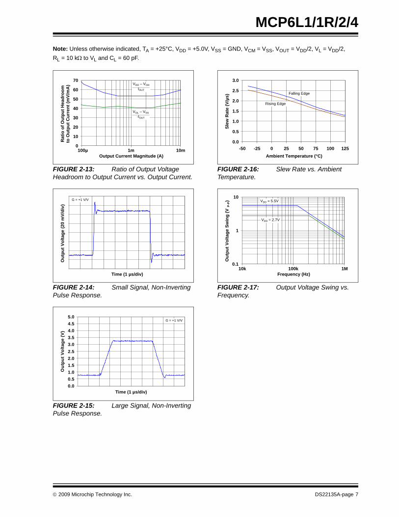
Note: Unless otherwise indicated, TA = +25°C, VDD = +5.0V, VSS = GND, VCM = VSS, VOUT = VDD/2, VL = VDD/2, RL = 10 kΩ to VL and CL = 60 pF.FIGURE 2-13: Ratio of Output Voltage Headroom to Output Current vs. Output Current.
FIGURE 2-14: Small Signal, Non-Inverting Pulse Response.
FIGURE 2-15: Large Signal, Non-Inverting Pulse Response.
FIGURE 2-16: Slew Rate vs. Ambient Temperature.
FIGURE 2-17: Output Voltage Swing vs. Frequency.
0
10
20
30
40
50
60
70
1.E-04 1.E-03 1.E-02Output Current Magnitude (A)
Rat
io o
f Out
put H
eadr
oom
to O
utpu
t Cur
rent
(mV/
mA
)
100µ 10m1m
VDD – VOH
IOUT
VOL – VSS
-IOUT
2.42
2.44
2.46
2.48
2.50
2.52
2.54
2.56
2.58
0.E+00 1.E-06 2.E-06 3.E-06 4.E-06 5.E-06 6.E-06 7.E-06 8.E-06 9.E-06 1.E-05
Time (1 µs/div)
Out
put V
olta
ge (2
0 m
V/di
v)
G = +1 V/V
0.00.51.01.52.02.53.03.54.04.55.0
0.E+00 1.E-06 2.E-06 3.E-06 4.E-06 5.E-06 6.E-06 7.E-06 8.E-06 9.E-06 1.E-05
Time (1 µs/div)
Out
put V
olta
ge (V
)
G = +1 V/V
0.0
0.5
1.0
1.5
2.0
2.5
3.0
-50 -25 0 25 50 75 100 125Ambient Temperature (°C)
Slew
Rat
e (V
/µs)
Rising Edge
Falling Edge
0.1
1
10
1.E+04 1.E+05 1.E+06Frequency (Hz)
Out
put V
olta
ge S
win
g (V
P-P) VDD = 5.5V
10k 100k 1M
VDD = 2.7V
© 2009 Microchip Technology Inc. DS22135A-page 7

MCP6L1/1R/2/4
NOTES:DS22135A-page 8 © 2009 Microchip Technology Inc.
MCP6L1/1R/2/4
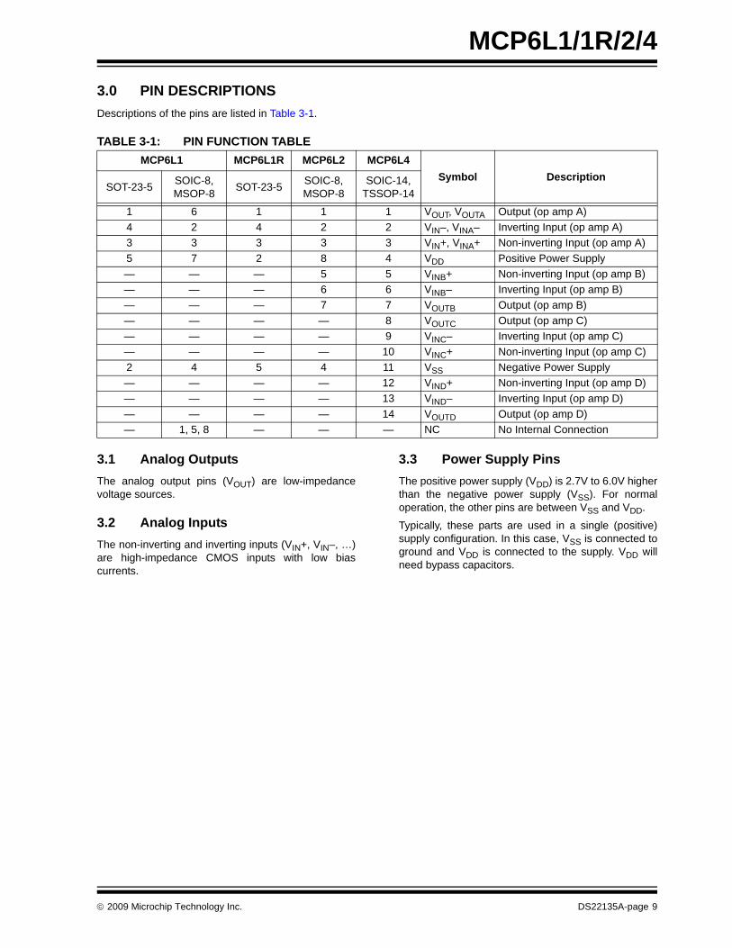
3.0 PIN DESCRIPTIONSDescriptions of the pins are listed in Table 3-1.
TABLE 3-1: PIN FUNCTION TABLE
3.1 Analog OutputsThe analog output pins (VOUT) are low-impedancevoltage sources.
3.2 Analog InputsThe non-inverting and inverting inputs (VIN+, VIN–, …)are high-impedance CMOS inputs with low biascurrents.
3.3 Power Supply PinsThe positive power supply (VDD) is 2.7V to 6.0V higherthan the negative power supply (VSS). For normaloperation, the other pins are between VSS and VDD.
Typically, these parts are used in a single (positive)supply configuration. In this case, VSS is connected toground and VDD is connected to the supply. VDD willneed bypass capacitors.
MCP6L1 MCP6L1R MCP6L2 MCP6L4Symbol Description
SOT-23-5 SOIC-8,MSOP-8 SOT-23-5 SOIC-8,
MSOP-8SOIC-14,
TSSOP-14
1 6 1 1 1 VOUT, VOUTA Output (op amp A)4 2 4 2 2 VIN–, VINA– Inverting Input (op amp A)3 3 3 3 3 VIN+, VINA+ Non-inverting Input (op amp A)5 7 2 8 4 VDD Positive Power Supply— — — 5 5 VINB+ Non-inverting Input (op amp B)— — — 6 6 VINB– Inverting Input (op amp B)— — — 7 7 VOUTB Output (op amp B)— — — — 8 VOUTC Output (op amp C)— — — — 9 VINC– Inverting Input (op amp C)— — — — 10 VINC+ Non-inverting Input (op amp C)2 4 5 4 11 VSS Negative Power Supply— — — — 12 VIND+ Non-inverting Input (op amp D)— — — — 13 VIND– Inverting Input (op amp D)— — — — 14 VOUTD Output (op amp D)— 1, 5, 8 — — — NC No Internal Connection
© 2009 Microchip Technology Inc. DS22135A-page 9

MCP6L1/1R/2/4
NOTES:DS22135A-page 10 © 2009 Microchip Technology Inc.
MCP6L1/1R/2/4
4.0 APPLICATION INFORMATIONThe MCP6L1/1R/2/4 family of op amps is manufac-tured using Microchip’s state of the art CMOS process.They are unity-gain stable and suitable for a wide rangeof general purpose applications.
4.1 Inputs
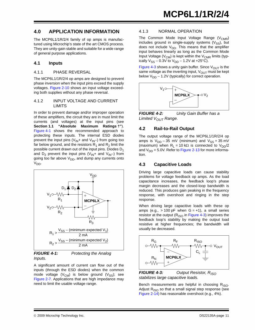
4.1.1 PHASE REVERSALThe MCP6L1/1R/2/4 op amps are designed to preventphase inversion when the input pins exceed the supplyvoltages. Figure 2-10 shows an input voltage exceed-ing both supplies without any phase reversal.
4.1.2 INPUT VOLTAGE AND CURRENT LIMITS
In order to prevent damage and/or improper operationof these amplifiers, the circuit they are in must limit thecurrents (and voltages) at the input pins (seeSection 1.1 “Absolute Maximum Ratings †”).Figure 4-1 shows the recommended approach toprotecting these inputs. The internal ESD diodesprevent the input pins (VIN+ and VIN–) from going toofar below ground, and the resistors R1 and R2 limit thepossible current drawn out of the input pins. Diodes D1and D2 prevent the input pins (VIN+ and VIN–) fromgoing too far above VDD, and dump any currents ontoVDD.
FIGURE 4-1: Protecting the Analog Inputs.A significant amount of current can flow out of theinputs (through the ESD diodes) when the commonmode voltage (VCM) is below ground (VSS); seeFigure 2-7. Applications that are high impedance mayneed to limit the usable voltage range.
4.1.3 NORMAL OPERATIONThe Common Mode Input Voltage Range (VCMR)includes ground in single-supply systems (VSS), butdoes not include VDD. This means that the amplifierinput behaves linearly as long as the Common ModeInput Voltage (VCM) is kept within the VCMR limits (typ-ically VSS – 0.3V to VDD – 1.2V at +25°C).
Figure 4-3 shows a unity gain buffer. Since VOUT is thesame voltage as the inverting input, VOUT must be keptbelow VDD – 1.2V (typically) for correct operation.
FIGURE 4-2: Unity Gain Buffer has a Limited VOUT Range.
4.2 Rail-to-Rail OutputThe output voltage range of the MCP6L1/1R/2/4 opamps is VDD – 35 mV (minimum) and VSS + 35 mV(maximum) when RL = 10 kΩ is connected to VDD/2and VDD = 5.0V. Refer to Figure 2-13 for more informa-tion.
4.3 Capacitive LoadsDriving large capacitive loads can cause stabilityproblems for voltage feedback op amps. As the loadcapacitance increases, the feedback loop’s phasemargin decreases and the closed-loop bandwidth isreduced. This produces gain peaking in the frequencyresponse, with overshoot and ringing in the stepresponse.
When driving large capacitive loads with these opamps (e.g., > 100 pF when G = +1), a small seriesresistor at the output (RISO in Figure 4-3) improves thefeedback loop’s stability by making the output loadresistive at higher frequencies; the bandwidth willusually be decreased.
FIGURE 4-3: Output Resistor, RISO stabilizes large capacitive loads.Bench measurements are helpful in choosing RISO.Adjust RISO so that a small signal step response (seeFigure 2-14) has reasonable overshoot (e.g., 4%).
V1
MCP6LXR1
VDD
D1
R1 >VSS – (minimum expected V1)
2 mA
R2 >VSS – (minimum expected V2)
2 mA
V2R2
D2
R3
V1
MCP6LX V2
RISOVOUT
CLMCP6LX
RFRG
RN
© 2009 Microchip Technology Inc. DS22135A-page 11
MCP6L1/1R/2/4
4.4 Supply BypassWith this family of operational amplifiers, the powersupply pin (VDD for single supply) should have a localbypass capacitor (i.e., 0.01 µF to 0.1 µF) within 2 mmfor good high frequency performance. It also needs abulk capacitor (i.e., 1 µF or larger) within 100 mm toprovide large, slow currents. This bulk capacitor can beshared with other nearby analog parts.4.5 Unused Op AmpsAn unused op amp in a quad package (e.g., MCP6L4)should be configured as shown in Figure 4-4. Thesecircuits prevent the output from toggling and causingcrosstalk. Circuit A sets the op amp at its minimumnoise gain. The resistor divider produces any desiredreference voltage within the output voltage range of theop amp; the op amp buffers that reference voltage.Circuit B uses the minimum number of componentsand operates as a comparator, but it may draw morecurrent.
FIGURE 4-4: Unused Op Amps.
4.6 PCB Surface LeakageIn applications where low input bias current is critical,PCB (printed circuit board) surface leakage effectsneed to be considered. Surface leakage is caused byhumidity, dust or other contamination on the board.Under low humidity conditions, a typical resistancebetween nearby traces is 1012Ω. A 5V difference wouldcause 5 pA of current to flow; this is greater than thisfamily’s bias current at 25°C (1 pA, typical).
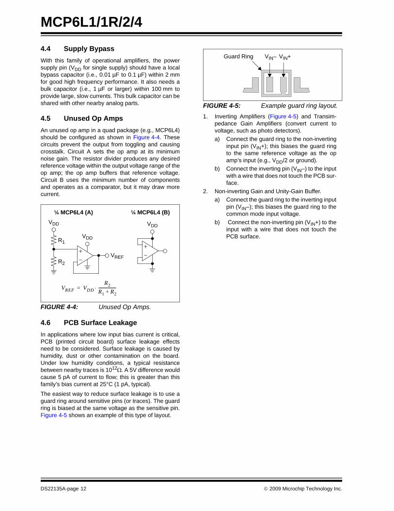
The easiest way to reduce surface leakage is to use aguard ring around sensitive pins (or traces). The guardring is biased at the same voltage as the sensitive pin.Figure 4-5 shows an example of this type of layout.
FIGURE 4-5: Example guard ring layout.1. Inverting Amplifiers (Figure 4-5) and Transim-
pedance Gain Amplifiers (convert current tovoltage, such as photo detectors).a) Connect the guard ring to the non-inverting
input pin (VIN+); this biases the guard ringto the same reference voltage as the opamp’s input (e.g., VDD/2 or ground).
b) Connect the inverting pin (VIN–) to the inputwith a wire that does not touch the PCB sur-face.
2. Non-inverting Gain and Unity-Gain Buffer.a) Connect the guard ring to the inverting input
pin (VIN–); this biases the guard ring to thecommon mode input voltage.
b) Connect the non-inverting pin (VIN+) to theinput with a wire that does not touch thePCB surface.VDD
VDD
¼ MCP6L4 (A) ¼ MCP6L4 (B)
R1
R2
VDD
VREF
VREF VDDR2
R1 R2+------------------⋅=
Guard Ring VIN– VIN+
DS22135A-page 12 © 2009 Microchip Technology Inc.
MCP6L1/1R/2/4
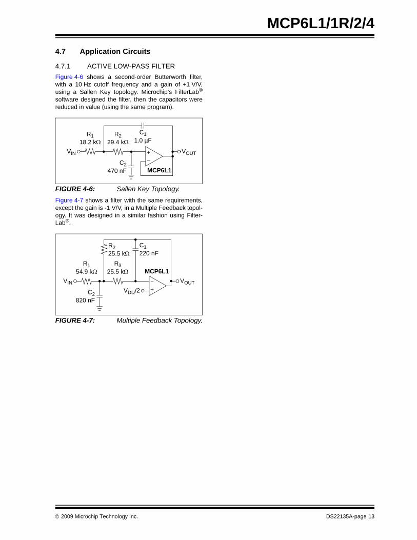
4.7 Application Circuits4.7.1 ACTIVE LOW-PASS FILTERFigure 4-6 shows a second-order Butterworth filter,with a 10 Hz cutoff frequency and a gain of +1 V/V,using a Sallen Key topology. Microchip’s FilterLab®
software designed the filter, then the capacitors werereduced in value (using the same program).
FIGURE 4-6: Sallen Key Topology.Figure 4-7 shows a filter with the same requirements,except the gain is -1 V/V, in a Multiple Feedback topol-ogy. It was designed in a similar fashion using Filter-Lab®.
FIGURE 4-7: Multiple Feedback Topology.
R1
VIN VOUT
R218.2 kΩ 29.4 kΩ
MCP6L1C2
470 nF
C11.0 µF
R1
VIN VOUT
R354.9 kΩ 25.5 kΩ MCP6L1
C2820 nF
C1220 nF
VDD/2
R225.5 kΩ
© 2009 Microchip Technology Inc. DS22135A-page 13

MCP6L1/1R/2/4
NOTES:DS22135A-page 14 © 2009 Microchip Technology Inc.
MCP6L1/1R/2/4
5.0 DESIGN AIDSMicrochip provides the basic design aids needed forthe MCP6L1/1R/2/4 family of op amps.
5.1 FilterLab® SoftwareMicrochip’s FilterLab® software is an innovativesoftware tool that simplifies analog active filter (usingop amps) design. Available at no cost from the Micro-chip web site at www.microchip.com/filterlab, the Filter-Lab design tool provides full schematic diagrams of thefilter circuit with component values. It also outputs thefilter circuit in SPICE format, which can be used withthe macro model to simulate actual filter performance.
5.2 Microchip Advanced Part Selector (MAPS)
MAPS is a software tool that helps efficiently identifyMicrochip devices that fit a particular design require-ment. Available at no cost from the Microchip websiteat www.microchip.com/maps, the MAPS is an overallselection tool for Microchip’s product portfolio thatincludes Analog, Memory, MCUs and DSCs. Using thistool, a customer can define a filter to sort features for aparametric search of devices and export side-by-sidetechnical comparison reports. Helpful links are alsoprovided for Data sheets, Purchase and Sampling ofMicrochip parts.
5.3 Analog Demonstration and Evaluation Boards
Microchip offers a broad spectrum of Analog Demon-stration and Evaluation Boards that are designed tohelp customers achieve faster time to market. For acomplete listing of these boards and their correspond-ing user’s guides and technical information, visit theMicrochip web site at www.microchip.com/analogtools.
Some boards that are especially useful are:
• MCP6XXX Amplifier Evaluation Board 1• MCP6XXX Amplifier Evaluation Board 2• MCP6XXX Amplifier Evaluation Board 3• MCP6XXX Amplifier Evaluation Board 4• Active Filter Demo Board Kit• P/N VSUPEV2: 5/6-Pin SOT-23 Evaluation Board• P/N SOIC8EV: 8-Pin SOIC/MSOP/TSSOP/DIP
Evaluation Board• P/N SOIC14EV: 14-Pin SOIC/TSSOP/DIP Evalu-
ation Board
5.4 Application NotesThe following Microchip Application Notes areavailable on the Microchip web site at www.microchip.com/appnotes and are recommended as supplementalreference resources.
ADN003: “Select the Right Operational Amplifier foryour Filtering Circuits”, DS21821
AN722: “Operational Amplifier Topologies and DCSpecifications”, DS00722
AN723: “Operational Amplifier AC Specifications andApplications”, DS00723
AN884: “Driving Capacitive Loads With Op Amps”,DS00884
AN990: “Analog Sensor Conditioning Circuits – AnOverview”, DS00990
© 2009 Microchip Technology Inc. DS22135A-page 15

MCP6L1/1R/2/4
NOTES:DS22135A-page 16 © 2009 Microchip Technology Inc.
MCP6L1/1R/2/4
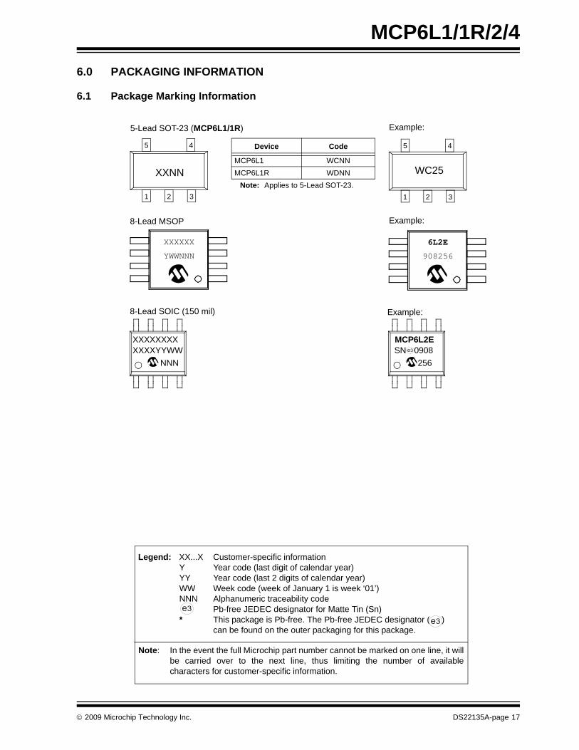
6.0 PACKAGING INFORMATION
6.1 Package Marking Information
1 2 3
5 4
5-Lead SOT-23 (MCP6L1/1R) Example:
XXNN
1 2 3
5 4
WC25
Device Code
MCP6L1 WCNNMCP6L1R WDNN
Note: Applies to 5-Lead SOT-23.
Legend: XX...X Customer-specific informationY Year code (last digit of calendar year)YY Year code (last 2 digits of calendar year)WW Week code (week of January 1 is week ‘01’)NNN Alphanumeric traceability code Pb-free JEDEC designator for Matte Tin (Sn)* This package is Pb-free. The Pb-free JEDEC designator ( )
can be found on the outer packaging for this package.
Note: In the event the full Microchip part number cannot be marked on one line, it willbe carried over to the next line, thus limiting the number of availablecharacters for customer-specific information.
3e
3e
8-Lead SOIC (150 mil) Example:
XXXXXXXXXXXXYYWW
NNN
MCP6L2ESN^^0908
2563e
8-Lead MSOP Example:
XXXXXX
YWWNNN
6L2E
908256
© 2009 Microchip Technology Inc. DS22135A-page 17
MCP6L1/1R/2/4
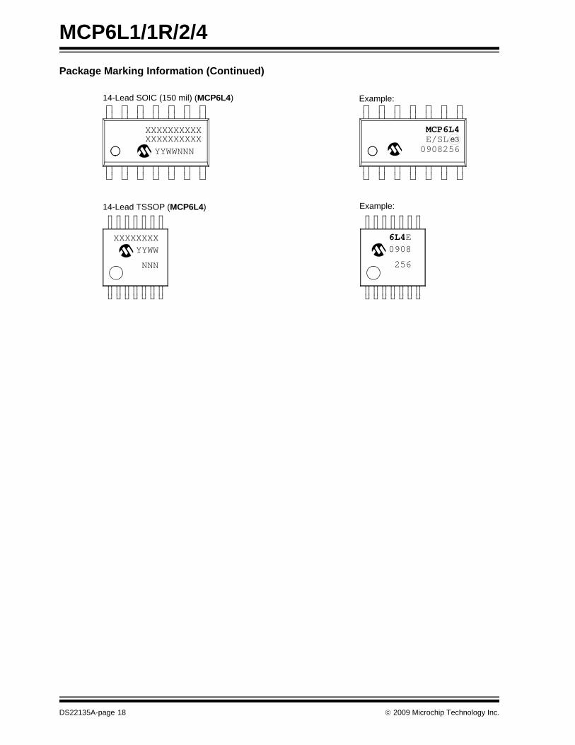
Package Marking Information (Continued)14-Lead TSSOP (MCP6L4) Example:
14-Lead SOIC (150 mil) (MCP6L4) Example:
XXXXXXXXXX
YYWWNNN
XXXXXXXXYYWW
NNN
XXXXXXXXXXMCP6L4
0908256
6L4E0908
256
E/SL^ 3̂e
DS22135A-page 18 © 2009 Microchip Technology Inc.
MCP6L1/1R/2/4
���������� ��������� �������� ������������������
�������� ��� � ��� �����!�"��!����#�����$! ����!�%�� �������#�$ ��� �����!�%�� �������#�$ ��� � �������#� &� !���������� �� �! ��� ��� � ���������!�#�� �������� �����"�'���(��
)�*+ )� ������ � ������� �� #������� &��#�,��$ � ��-��-�#��$#�#�� ���� �
����� .���#� ��� #��$�� �#���/�� �!��-��� 0�� � � �#� ����������1��/������� ��%���#��������# !��#��##+22---�������������2��/�����
3��# ��44��"�"����� � ����4���# ��5 56� ��7
5$�8 ���%�1�� 5 (4 �!�1�#�� ���(�)�*6$# �! �4 �!�1�#�� � �����)�*6, �����9 ���# � ���� : ���(���! !�1��/�� �����/� �� ��;� : �����#��!�%% �� ���� : ���(6, �����<�!#� " ���� : �������! !�1��/�� �<�!#� "� ���� : ��;�6, �����4 ��#� � ���� : ����.��#�4 ��#� 4 ���� : ��=�.��#���# 4� ���( : ��;�.��#����� � �> : ��>4 �!�����/� � ���; : ���=4 �!�<�!#� 8 ���� : ��(�
φ
Nb
E
E1
D
1 2 3
e
e1
A
A1
A2 c
L
L1
�������� � �������� ���-��� *�����)
© 2009 Microchip Technology Inc. DS22135A-page 19
MCP6L1/1R/2/4
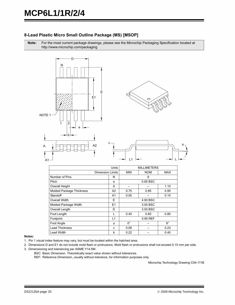
���������� �� ����������� �����!�"��� ���� ���
�������� 1�����,� $�����! &�% �#$� �����,���0�8$#��$ #�8 �����# !�-�#����#� ���#�� !��� ���� ��� � ��� �����!�"��!����#�����$! ����!�%�� �������#�$ ��� �����!�%�� �������#�$ ��� � �������#� &� !����(���� �� �! ��� ��� � ���������!�#�� �������� �����"�'���(��
)�*+ )� ������ � ������� �� #������� &��#�,��$ � ��-��-�#��$#�#�� ���� ��".+ � % � �� ���� � ���0�$ $�����-�#��$#�#�� ���� 0�%�����%����#����$�� ������
����� .���#� ��� #��$�� �#���/�� �!��-��� 0�� � � �#� ����������1��/������� ��%���#��������# !��#��##+22---�������������2��/�����
3��# ��44��"�"����� � ����4���# ��5 56� ��7
5$�8 ���%�1�� 5 ;1�#�� ��=(�)�*6, �����9 ���# � : : �������! !�1��/�� �����/� �� ���( ��;( ���(�#��!�%%� �� ���� : ���(6, �����<�!#� " �����)�*���! !�1��/�� �<�!#� "� �����)�*6, �����4 ��#� � �����)�*.��#�4 ��#� 4 ���� ��=� ��;�.��#���# 4� ���(��"..��#����� � �> : ;>4 �!�����/� � ���; : ����4 �!�<�!#� 8 ���� : ����
D
N
E
E1
NOTE 1
1 2e
b
A
A1
A2c
L1 L
φ
�������� � �������� ���-��� *�����)
DS22135A-page 20 © 2009 Microchip Technology Inc.
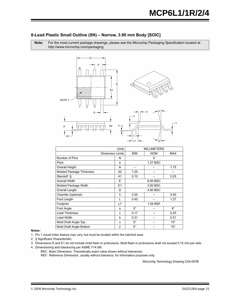
MCP6L1/1R/2/4
���������� ��������� ��������#������$%��&'(����)��*����+,�
�������� 1�����,� $�����! &�% �#$� �����,���0�8$#��$ #�8 �����# !�-�#����#� ���#�� !��� ���� ?������%����#�*�����# �� #����� ��� � ��� �����!�"��!����#�����$! ����!�%�� �������#�$ ��� �����!�%�� �������#�$ ��� � �������#� &� !����(���� �� �! ��� ��� � ���������!�#�� �������� �����"�'���(��
)�*+ )� ������ � ������� �� #������� &��#�,��$ � ��-��-�#��$#�#�� ���� ��".+ � % � �� ���� � ���0�$ $�����-�#��$#�#�� ���� 0�%�����%����#����$�� ������
����� .���#� ��� #��$�� �#���/�� �!��-��� 0�� � � �#� ����������1��/������� ��%���#��������# !��#��##+22---�������������2��/�����
3��# ��44��"�"����� � ����4���# ��5 56� ��7
5$�8 ���%�1�� 5 ;1�#�� �����)�*6, �����9 ���# � : : ���(���! !�1��/�� �����/� �� ���( : :�#��!�%%��? �� ���� : ���(6, �����<�!#� " =����)�*���! !�1��/�� �<�!#� "� �����)�*6, �����4 ��#� � �����)�**���% ��@�#�����A � ���( : ��(�.��#�4 ��#� 4 ���� : ����.��#���# 4� ������"..��#����� � �> : ;>4 �!�����/� � ���� : ���(4 �!�<�!#� 8 ���� : ��(����!����%#����� ��� � (> : �(>���!����%#����� �)�##�� � (> : �(>
D
Ne
E
E1
NOTE 1
1 2 3
b
A
A1
A2
L
L1
c
h
h
φ
β
α
�������� � �������� ���-��� *���(�)
© 2009 Microchip Technology Inc. DS22135A-page 21
MCP6L1/1R/2/4
���������� ��������� ��������#������$%��&'(����)��*����+,�
����� .���#� ��� #��$�� �#���/�� �!��-��� 0�� � � �#� ����������1��/������� ��%���#��������# !��#��##+22---�������������2��/�����
DS22135A-page 22 © 2009 Microchip Technology Inc.
MCP6L1/1R/2/4
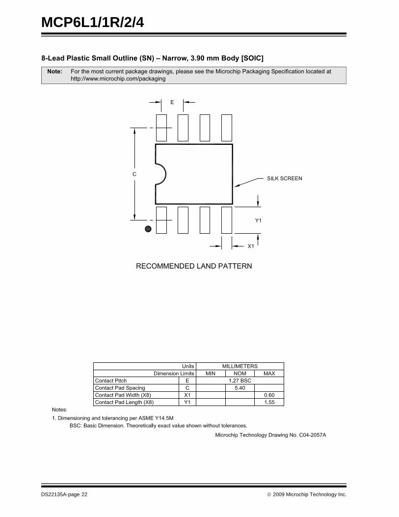
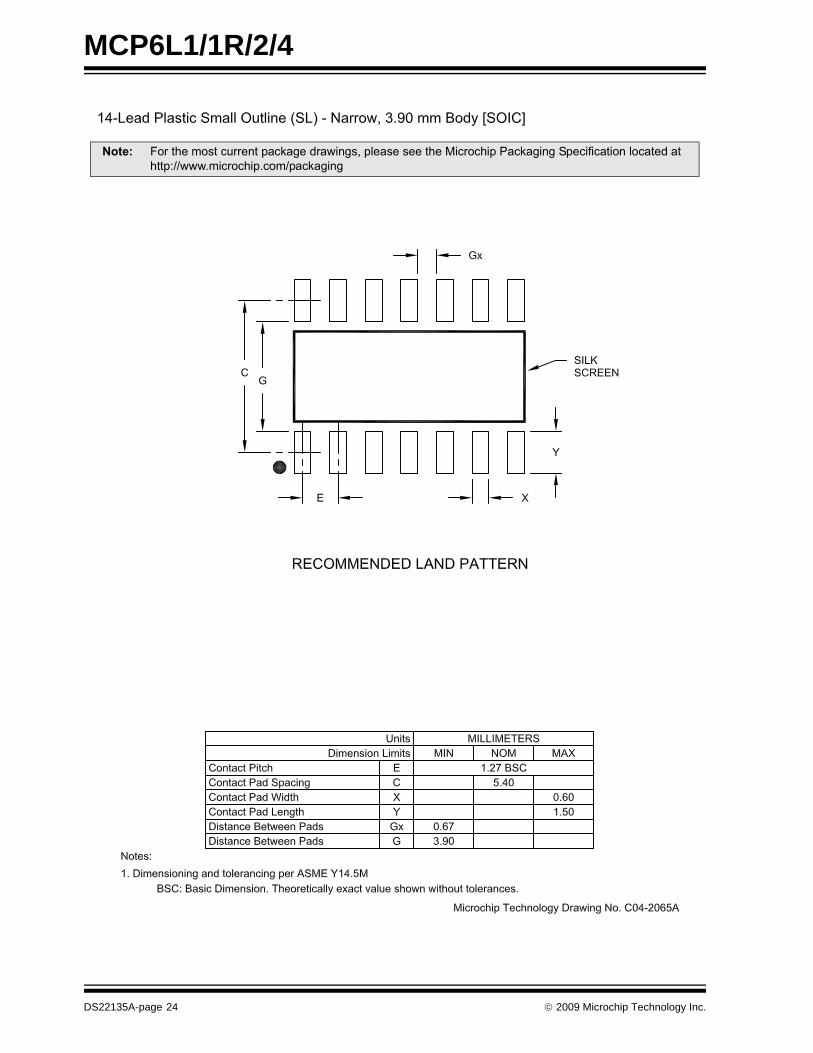
-.��������� ��������� ��������#������$%��&'(����)��*����+,�
�������� 1�����,� $�����! &�% �#$� �����,���0�8$#��$ #�8 �����# !�-�#����#� ���#�� !��� ���� ?������%����#�*�����# �� #����� ��� � ��� �����!�"��!����#�����$! ����!�%�� �������#�$ ��� �����!�%�� �������#�$ ��� � �������#� &� !����(���� �� �! ��� ��� � ���������!�#�� �������� �����"�'���(��
)�*+ )� ������ � ������� �� #������� &��#�,��$ � ��-��-�#��$#�#�� ���� ��".+ � % � �� ���� � ���0�$ $�����-�#��$#�#�� ���� 0�%�����%����#����$�� ������
����� .���#� ��� #��$�� �#���/�� �!��-��� 0�� � � �#� ����������1��/������� ��%���#��������# !��#��##+22---�������������2��/�����
3��# ��44��"�"����� � ����4���# ��5 56� ��7
5$�8 ���%�1�� 5 ��1�#�� �����)�*6, �����9 ���# � : : ���(���! !�1��/�� �����/� �� ���( : :�#��!�%%��? �� ���� : ���(6, �����<�!#� " =����)�*���! !�1��/�� �<�!#� "� �����)�*6, �����4 ��#� � ;�=(�)�**���% ��@�#�����A � ���( : ��(�.��#�4 ��#� 4 ���� : ����.��#���# 4� ������"..��#����� � �> : ;>4 �!�����/� � ���� : ���(4 �!�<�!#� 8 ���� : ��(����!����%#����� ��� � (> : �(>���!����%#����� �)�##�� � (> : �(>
NOTE 1
N
D
E
E1
1 2 3
b
e
A
A1
A2
L
L1
c
h
h α
β
φ
�������� � �������� ���-��� *���=()
© 2009 Microchip Technology Inc. DS22135A-page 23
MCP6L1/1R/2/4
����� .���#� ��� #��$�� �#���/�� �!��-��� 0�� � � �#� ����������1��/������� ��%���#��������# !��#��##+22---�������������2��/�����
DS22135A-page 24 © 2009 Microchip Technology Inc.
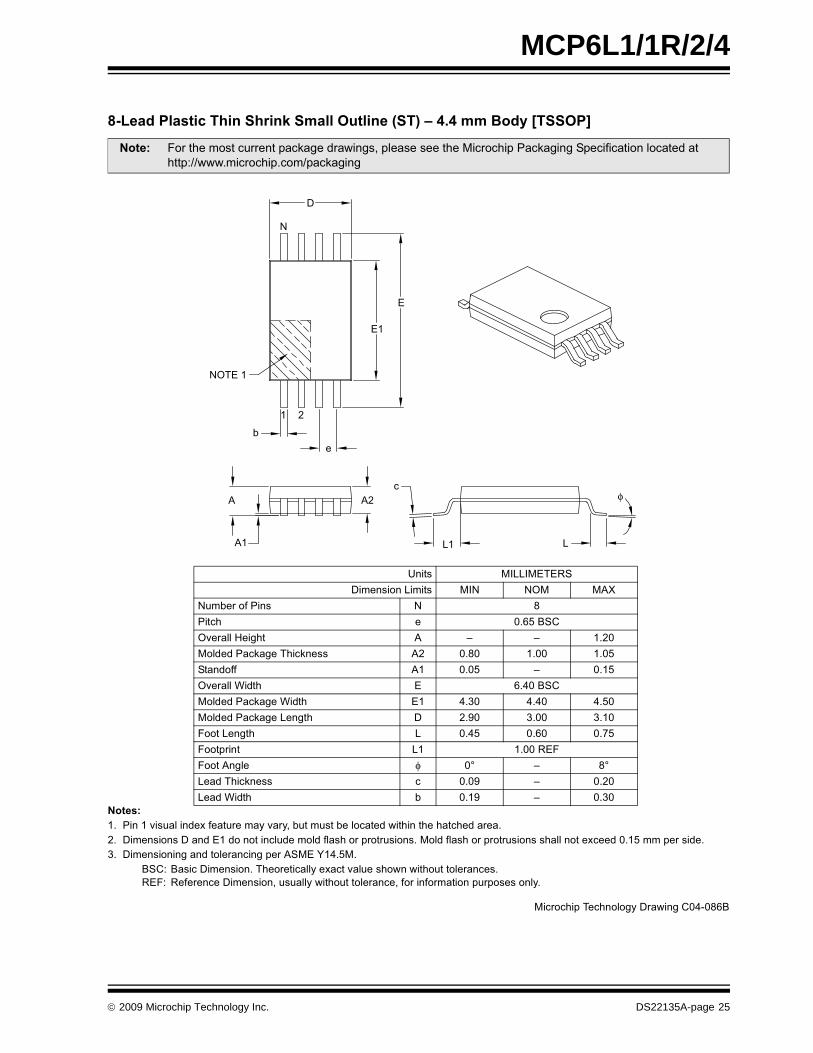
MCP6L1/1R/2/4
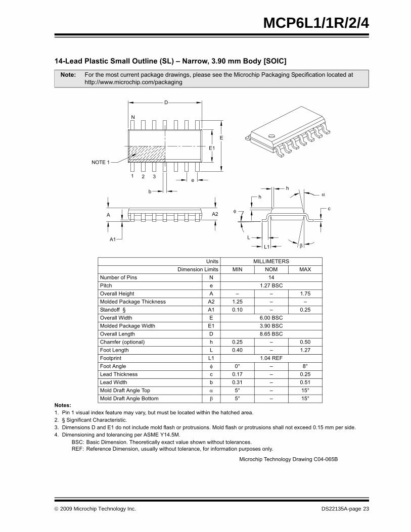
���������� ���/ ���/� �!�������� ��������#�.&.����)��*�������
�������� 1�����,� $�����! &�% �#$� �����,���0�8$#��$ #�8 �����# !�-�#����#� ���#�� !��� ���� ��� � ��� �����!�"��!����#�����$! ����!�%�� �������#�$ ��� �����!�%�� �������#�$ ��� � �������#� &� !����(���� �� �! ��� ��� � ���������!�#�� �������� �����"�'���(��
)�*+ )� ������ � ������� �� #������� &��#�,��$ � ��-��-�#��$#�#�� ���� ��".+ � % � �� ���� � ���0�$ $�����-�#��$#�#�� ���� 0�%�����%����#����$�� ������
����� .���#� ��� #��$�� �#���/�� �!��-��� 0�� � � �#� ����������1��/������� ��%���#��������# !��#��##+22---�������������2��/�����
3��# ��44��"�"����� � ����4���# ��5 56� ��7
5$�8 ���%�1�� 5 ;1�#�� ��=(�)�*6, �����9 ���# � : : �������! !�1��/�� �����/� �� ��;� ���� ���(�#��!�%%� �� ���( : ���(6, �����<�!#� " =����)�*���! !�1��/�� �<�!#� "� ���� ���� ��(����! !�1��/�� �4 ��#� � ���� ���� ����.��#�4 ��#� 4 ���( ��=� ���(.��#���# 4� ������"..��#����� � �> : ;>4 �!�����/� � ���� : ����4 �!�<�!#� 8 ���� : ����
D
N
E
E1
NOTE 1
1 2
be
cA
A1
A2
L1 L
φ
�������� � �������� ���-��� *���;=)
© 2009 Microchip Technology Inc. DS22135A-page 25

MCP6L1/1R/2/4
NOTES:DS22135A-page 26 © 2009 Microchip Technology Inc.
MCP6L1/1R/2/4
APPENDIX A: REVISION HISTORY
Revision A (March 2009)• Original Release of this Document.
© 2009 Microchip Technology Inc. DS22135A-page 29
MCP6L1/1R/2/4
NOTES:DS22135A-page 30 © 2009 Microchip Technology Inc.
MCP6L1/1R/2/4
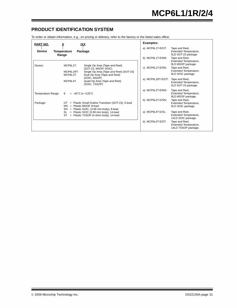
PRODUCT IDENTIFICATION SYSTEMTo order or obtain information, e.g., on pricing or delivery, refer to the factory or the listed sales office.
Device: MCP6L1T: Single Op Amp (Tape and Reel)
(SOT-23, MSOP, SOIC)MCP6L1RT: Single Op Amp (Tape and Reel) (SOT-23)MCP6L2T: Dual Op Amp (Tape and Reel)
(SOIC, MSOP)MCP6L4T: Quad Op Amp (Tape and Reel)
(SOIC, TSSOP)
Temperature Range: E = -40°C to +125°C
Package: OT = Plastic Small Outline Transistor (SOT-23), 5-leadMS = Plastic MSOP, 8-leadSN = Plastic SOIC, (3.99 mm body), 8-leadSL = Plastic SOIC (3.99 mm body), 14-leadST = Plastic TSSOP (4.4mm body), 14-lead
PART NO. X /XX
PackageTemperatureRange
Device
Examples:a) MCP6L1T-E/OT: Tape and Reel,
Extended Temperature,5LD SOT-23 package
b) MCP6L1T-E/MS: Tape and Reel,Extended Temperature,8LD MSOP package.
c) MCP6L1T-E/SN: Tape and Reel,Extended Temperature,8LD SOIC package.
a) MCP6L1RT-E/OT: Tape and Reel,Extended Temperature,5LD SOT-23 package.
a) MCP6L2T-E/MS: Tape and Reel,Extended Temperature,8LD MSOP package.
b) MCP6L2T-E/SN: Tape and Reel,Extended Temperature,8LD SOIC package.
a) MCP6L4T-E/SL: Tape and Reel,Extended Temperature,14LD SOIC package.
b) MCP6L4T-E/ST: Tape and Reel,Extended Temperature,14LD TSSOP package.
© 2009 Microchip Technology Inc. DS22135A-page 31

MCP6L1/1R/2/4
NOTES:DS22135A-page 32 © 2009 Microchip Technology Inc.
Note the following details of the code protection feature on Microchip devices:• Microchip products meet the specification contained in their particular Microchip Data Sheet.
• Microchip believes that its family of products is one of the most secure families of its kind on the market today, when used in the intended manner and under normal conditions.
• There are dishonest and possibly illegal methods used to breach the code protection feature. All of these methods, to our knowledge, require using the Microchip products in a manner outside the operating specifications contained in Microchip’s Data Sheets. Most likely, the person doing so is engaged in theft of intellectual property.
• Microchip is willing to work with the customer who is concerned about the integrity of their code.
• Neither Microchip nor any other semiconductor manufacturer can guarantee the security of their code. Code protection does not mean that we are guaranteeing the product as “unbreakable.”
Code protection is constantly evolving. We at Microchip are committed to continuously improving the code protection features of ourproducts. Attempts to break Microchip’s code protection feature may be a violation of the Digital Millennium Copyright Act. If such actsallow unauthorized access to your software or other copyrighted work, you may have a right to sue for relief under that Act.
Information contained in this publication regarding deviceapplications and the like is provided only for your convenienceand may be superseded by updates. It is your responsibility toensure that your application meets with your specifications.MICROCHIP MAKES NO REPRESENTATIONS ORWARRANTIES OF ANY KIND WHETHER EXPRESS ORIMPLIED, WRITTEN OR ORAL, STATUTORY OROTHERWISE, RELATED TO THE INFORMATION,INCLUDING BUT NOT LIMITED TO ITS CONDITION,QUALITY, PERFORMANCE, MERCHANTABILITY ORFITNESS FOR PURPOSE. Microchip disclaims all liabilityarising from this information and its use. Use of Microchipdevices in life support and/or safety applications is entirely atthe buyer’s risk, and the buyer agrees to defend, indemnify andhold harmless Microchip from any and all damages, claims,suits, or expenses resulting from such use. No licenses areconveyed, implicitly or otherwise, under any Microchipintellectual property rights.
© 2009 Microchip Technology Inc.
Trademarks
The Microchip name and logo, the Microchip logo, Accuron, dsPIC, KEELOQ, KEELOQ logo, MPLAB, PIC, PICmicro, PICSTART, rfPIC, SmartShunt and UNI/O are registered trademarks of Microchip Technology Incorporated in the U.S.A. and other countries.
FilterLab, Linear Active Thermistor, MXDEV, MXLAB, SEEVAL, SmartSensor and The Embedded Control Solutions Company are registered trademarks of Microchip Technology Incorporated in the U.S.A.
Analog-for-the-Digital Age, Application Maestro, CodeGuard, dsPICDEM, dsPICDEM.net, dsPICworks, dsSPEAK, ECAN, ECONOMONITOR, FanSense, In-Circuit Serial Programming, ICSP, ICEPIC, Mindi, MiWi, MPASM, MPLAB Certified logo, MPLIB, MPLINK, mTouch, PICkit, PICDEM, PICDEM.net, PICtail, PIC32 logo, PowerCal, PowerInfo, PowerMate, PowerTool, REAL ICE, rfLAB, Select Mode, Total Endurance, WiperLock and ZENA are trademarks of Microchip Technology Incorporated in the U.S.A. and other countries.
SQTP is a service mark of Microchip Technology Incorporated in the U.S.A.
All other trademarks mentioned herein are property of their respective companies.
© 2009, Microchip Technology Incorporated, Printed in the U.S.A., All Rights Reserved.
Printed on recycled paper.
DS22135A-page 33
Microchip received ISO/TS-16949:2002 certification for its worldwide headquarters, design and wafer fabrication facilities in Chandler and Tempe, Arizona; Gresham, Oregon and design centers in California and India. The Company’s quality system processes and procedures are for its PIC® MCUs and dsPIC® DSCs, KEELOQ® code hopping devices, Serial EEPROMs, microperipherals, nonvolatile memory and analog products. In addition, Microchip’s quality system for the design and manufacture of development systems is ISO 9001:2000 certified.
DS22135A-page 34 © 2009 Microchip Technology Inc.
AMERICASCorporate Office2355 West Chandler Blvd.Chandler, AZ 85224-6199Tel: 480-792-7200 Fax: 480-792-7277Technical Support: http://support.microchip.comWeb Address: www.microchip.comAtlantaDuluth, GA Tel: 678-957-9614 Fax: 678-957-1455BostonWestborough, MA Tel: 774-760-0087 Fax: 774-760-0088ChicagoItasca, IL Tel: 630-285-0071 Fax: 630-285-0075ClevelandIndependence, OH Tel: 216-447-0464 Fax: 216-447-0643DallasAddison, TX Tel: 972-818-7423 Fax: 972-818-2924DetroitFarmington Hills, MI Tel: 248-538-2250Fax: 248-538-2260KokomoKokomo, IN Tel: 765-864-8360Fax: 765-864-8387Los AngelesMission Viejo, CA Tel: 949-462-9523 Fax: 949-462-9608Santa ClaraSanta Clara, CA Tel: 408-961-6444Fax: 408-961-6445TorontoMississauga, Ontario, CanadaTel: 905-673-0699 Fax: 905-673-6509
ASIA/PACIFICAsia Pacific OfficeSuites 3707-14, 37th FloorTower 6, The GatewayHarbour City, KowloonHong KongTel: 852-2401-1200Fax: 852-2401-3431Australia - SydneyTel: 61-2-9868-6733Fax: 61-2-9868-6755China - BeijingTel: 86-10-8528-2100 Fax: 86-10-8528-2104China - ChengduTel: 86-28-8665-5511Fax: 86-28-8665-7889China - Hong Kong SARTel: 852-2401-1200 Fax: 852-2401-3431China - NanjingTel: 86-25-8473-2460Fax: 86-25-8473-2470China - QingdaoTel: 86-532-8502-7355Fax: 86-532-8502-7205China - ShanghaiTel: 86-21-5407-5533 Fax: 86-21-5407-5066China - ShenyangTel: 86-24-2334-2829Fax: 86-24-2334-2393China - ShenzhenTel: 86-755-8203-2660 Fax: 86-755-8203-1760China - WuhanTel: 86-27-5980-5300Fax: 86-27-5980-5118China - XiamenTel: 86-592-2388138 Fax: 86-592-2388130China - XianTel: 86-29-8833-7252Fax: 86-29-8833-7256China - ZhuhaiTel: 86-756-3210040 Fax: 86-756-3210049
ASIA/PACIFICIndia - BangaloreTel: 91-80-3090-4444 Fax: 91-80-3090-4080India - New DelhiTel: 91-11-4160-8631Fax: 91-11-4160-8632India - PuneTel: 91-20-2566-1512Fax: 91-20-2566-1513Japan - YokohamaTel: 81-45-471- 6166 Fax: 81-45-471-6122Korea - DaeguTel: 82-53-744-4301Fax: 82-53-744-4302Korea - SeoulTel: 82-2-554-7200Fax: 82-2-558-5932 or 82-2-558-5934Malaysia - Kuala LumpurTel: 60-3-6201-9857Fax: 60-3-6201-9859Malaysia - PenangTel: 60-4-227-8870Fax: 60-4-227-4068Philippines - ManilaTel: 63-2-634-9065Fax: 63-2-634-9069SingaporeTel: 65-6334-8870Fax: 65-6334-8850Taiwan - Hsin ChuTel: 886-3-572-9526Fax: 886-3-572-6459Taiwan - KaohsiungTel: 886-7-536-4818Fax: 886-7-536-4803Taiwan - TaipeiTel: 886-2-2500-6610 Fax: 886-2-2508-0102Thailand - BangkokTel: 66-2-694-1351Fax: 66-2-694-1350
EUROPEAustria - WelsTel: 43-7242-2244-39Fax: 43-7242-2244-393Denmark - CopenhagenTel: 45-4450-2828 Fax: 45-4485-2829France - ParisTel: 33-1-69-53-63-20 Fax: 33-1-69-30-90-79Germany - MunichTel: 49-89-627-144-0 Fax: 49-89-627-144-44Italy - Milan Tel: 39-0331-742611 Fax: 39-0331-466781Netherlands - DrunenTel: 31-416-690399 Fax: 31-416-690340Spain - MadridTel: 34-91-708-08-90Fax: 34-91-708-08-91UK - WokinghamTel: 44-118-921-5869Fax: 44-118-921-5820
Worldwide Sales and Service
02/04/09