Embed Size (px)
Citation preview

MCP6L71/1R/2/42 MHz, 150 µA Op Amps
Features• Gain Bandwidth Product: 2 MHz (typical)• Supply Current: IQ = 150 µA (typical)• Supply Voltage: 2.0V to 6.0V• Rail-to-Rail Input/Output• Extended Temperature Range: -40°C to +125°C• Available in Single, Dual and Quad Packages
Typical Applications• Portable Equipment• Photodiode Amplifier• Analog Filters• Notebooks and PDAs• Battery-Powered Systems
Design Aids• FilterLab® Software• MAPS (Microchip Advanced Part Selector)• Analog Demonstration and Evaluation Boards• Application Notes
Typical Application
DescriptionThe Microchip Technology Inc. MCP6L71/1R/2/4 familyof operational amplifiers (op amps) supports generalpurpose applications. The combination of rail-to-railinput and output, low quiescent current and bandwidthfit into many applications.This family has a 2 MHz Gain Bandwidth Product(GBWP) and a low 150 µA per amplifier quiescentcurrent. These op amps operate on supply voltagesbetween 2.0V and 6.0V, with rail-to-rail input and outputswing. They are available in the extended temperaturerange.
Package Types
Inverting Amplifier
MCP6L71
R1 R2
VREF
VIN VOUT
R3–
+
VIN-
MCP6L71SOIC, MSOP
VDD
1
2
3
4
8
7
6
5 NC
NCNC
VIN+VSS
VOUT
VINA-
MCP6L72SOIC, MSOP
VOUTB
1
2
3
4
8
7
6
5 VINB+
VDDVOUTA
VINA+
VSS
VINB-
VINA-
MCP6L74SOIC, TSSOP
VIND-1
2
3
4
14
13
12
11 VSS
VOUTDVOUTA
VINA+VDD
VIND+
5
6
7
10
9
8
VINB+ VINC+
VOUTC
VINB-
VOUTB
VINC-
VSS
1
2
3
5
4
VDDVOUT
VIN+ VIN-
VDD
MCP6L71RSOT-23-5
1
2
3
5
4
VSSVOUT
VIN+ VIN-
MCP6L71SOT-23-5
2009-2019 Microchip Technology Inc. DS20002145B-page 1

MCP6L71/1R/2/4
NOTES:DS20002145B-page 2 2009-2019 Microchip Technology Inc.
MCP6L71/1R/2/4
1.0 ELECTRICAL CHARACTERISTICS1.1 Absolute Maximum Ratings†VDD – VSS ........................................................................7.0VCurrent at Input Pins ....................................................±2 mAAnalog Inputs (VIN+ and VIN-)†† ...... VSS – 1.0V to VDD + 1.0VAll Other Inputs and Outputs ......... VSS – 0.3V to VDD + 0.3VDifference Input Voltage ...................................... |VDD – VSS|Output Short-Circuit Current ................................ContinuousCurrent at Output and Supply Pins ............................±30 mAStorage Temperature ....................................-65°C to +150°CJunction Temperature (TJ) .........................................+150°CESD Protection on All Pins (HBM/MM) 4 kV/400V
† Notice: Stresses above those listed under “AbsoluteMaximum Ratings” may cause permanent damage to thedevice. This is a stress rating only and functional operation ofthe device at those or any other conditions above thoseindicated in the operational listings of this specification is notimplied. Exposure to maximum rating conditions for extendedperiods may affect device reliability.†† See Section 4.1.2 “Input Voltage and Current Limits”.
1.2 Specifications
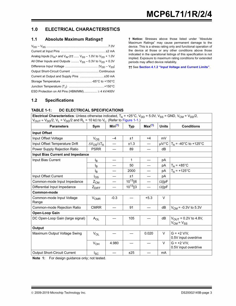
TABLE 1-1: DC ELECTRICAL SPECIFICATIONSElectrical Characteristics: Unless otherwise indicated, TA = +25°C, VDD = 5.0V, VSS = GND, VCM = VDD/2, VOUT VDD/2, VL = VDD/2 and RL = 10 kto VL. (Refer to Figure 1-1.)
Parameters Sym Min(1) Typ Max(1) Units Conditions
Input Offset Input Offset Voltage VOS –4 ±1 +4 mVInput Offset Temperature Drift VOS/TA — ±1.3 — µV/°C TA = -40°C to +125°CPower Supply Rejection Ratio PSRR — 89 — dBInput Bias Current and ImpedanceInput Bias Current IB — 1 — pA
IB — 50 — pA TA = +85°C IB — 2000 — pA TA = +125°C
Input Offset Current IOS — ±1 — pACommon-mode Input Impedance ZCM — 1013||6 — ||pFDifferential Input Impedance ZDIFF — 1013||3 — ||pFCommon-modeCommon-mode Input Voltage Range
VCMR -0.3 — +5.3 V
Common-mode Rejection Ratio CMRR — 91 — dB VCM = -0.3V to 5.3VOpen-Loop GainDC Open-Loop Gain (large signal) AOL — 105 — dB VOUT = 0.2V to 4.8V,
VCM = VSS OutputMaximum Output Voltage Swing VOL — — 0.020 V G = +2 V/V,
0.5V input overdrive VOH 4.980 — — V G = +2 V/V,
0.5V input overdrive Output Short-Circuit Current ISC — ±25 — mANote 1: For design guidance only; not tested.
2009-2019 Microchip Technology Inc. DS20002145B-page 3

MCP6L71/1R/2/4
TABLE 1-2: AC ELECTRICAL SPECIFICATIONS
TABLE 1-3: TEMPERATURE SPECIFICATIONS
Power SupplySupply Voltage VDD 2.0 — 6.0 VQuiescent Current per Amplifier IQ 50 150 240 µA IO = 0
Electrical Characteristics: Unless otherwise indicated, TA = +25°C, VDD = +2.0V to +5.5V, VSS = GND, VCM = VDD/2, VOUT VDD/2, VL = VDD/2, RL = 10 kto VL and CL = 60 pF. (Refer to Figure 1-1.)
Parameters Sym Min Typ Max Units Conditions
AC ResponseGain Bandwidth Product GBWP — 2.0 — MHzPhase Margin PM — 65 — ° G = +1 V/VSlew Rate SR — 0.9 — V/µsNoiseInput Noise Voltage Eni — 4.6 — µVP-P f = 0.1 Hz to 10 HzInput Noise Voltage Density eni — 19 — nV/Hz f = 10 kHzInput Noise Current Density ini — 3 — fA/Hz f = 1 kHz
TABLE 1-1: DC ELECTRICAL SPECIFICATIONS (CONTINUED)Electrical Characteristics: Unless otherwise indicated, TA = +25°C, VDD = 5.0V, VSS = GND, VCM = VDD/2, VOUT VDD/2, VL = VDD/2 and RL = 10 kto VL. (Refer to Figure 1-1.)
Parameters Sym Min(1) Typ Max(1) Units Conditions
Note 1: For design guidance only; not tested.
Electrical Characteristics: Unless otherwise indicated, VDD = +2.0V to +5.5V and VSS = GND.
Parameters Sym Min Typ Max Units Conditions
Temperature RangesSpecified Temperature Range TA -40 — +125 °COperating Temperature Range TA -40 — +125 °C Note 1Storage Temperature Range TA -65 — +150 °CThermal Package ResistancesThermal Resistance, 5-Lead SOT-23 JA — 256 — °C/WThermal Resistance, 8-Lead SOIC JA — 163 — °C/WThermal Resistance, 8-Lead MSOP JA — 206 — °C/WThermal Resistance, 14-Lead SOIC JA — 120 — °C/WThermal Resistance, 14-Lead TSSOP JA — 100 — °C/WNote 1: The Junction Temperature (TJ) must not exceed the absolute maximum specification of +150°C.
DS20002145B-page 4 2009-2019 Microchip Technology Inc.

MCP6L71/1R/2/4
1.3 Test CircuitsThe circuit used for most DC and AC tests is shown inFigure 1-1. This circuit can independently set VCM andVOUT; see Equation 1-1. Note that VCM is not thecircuit’s Common-mode voltage ((VP + VM)/2), and thatVOST includes VOS plus the effects (on the input offseterror, VOST) of temperature, CMRR, PSRR and AOL.EQUATION 1-1:
FIGURE 1-1: AC and DC Test Circuit for Most Specifications.
GDM RF RG=
VCM VP VDD 2+ 2=
VOUT VDD 2 VP VM– VOST 1 GDM+ + +=
Where:
GDM = Differential-mode Gain (V/V)VCM = Op Amp’s Common-mode
Input Voltage(V)
VOST = Op Amp’s Total Input OffsetVoltage
(mV)
VOST VIN– VIN+–=
VDD
MCP6L7X
RG RF
VOUTVM
CB2
CLRL
VL
CB1
100 k100 k
RG RF
VDD/2VP
100 k100 k
60 pF10 k
1 µF100 nF
VIN-
VIN+
CF6.8 pF
CF6.8 pF
+
–
2009-2019 Microchip Technology Inc. DS20002145B-page 5

MCP6L71/1R/2/4
NOTES:DS20002145B-page 6 2009-2019 Microchip Technology Inc.
MCP6L71/1R/2/4
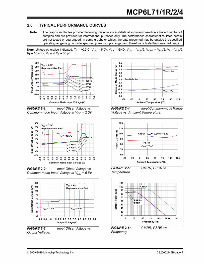
2.0 TYPICAL PERFORMANCE CURVESNote: Unless otherwise indicated, TA = +25°C, VDD = 5.0V, VSS = GND, VCM = VDD/2, VOUT VDD/2, VL = VDD/2,RL = 10 k to VL and CL = 60 pF.
FIGURE 2-1: Input Offset Voltage vs. Common-mode Input Voltage at VDD = 2.0V.
FIGURE 2-2: Input Offset Voltage vs. Common-mode Input Voltage at VDD = 5.5V.
FIGURE 2-3: Input Offset Voltage vs. Output Voltage.
FIGURE 2-4: Input Common-mode Range Voltage vs. Ambient Temperature.
FIGURE 2-5: CMRR, PSRR vs. Temperature.
FIGURE 2-6: CMRR, PSRR vs. Frequency.
Note: The graphs and tables provided following this note are a statistical summary based on a limited number ofsamples and are provided for informational purposes only. The performance characteristics listed hereinare not tested or guaranteed. In some graphs or tables, the data presented may be outside the specifiedoperating range (e.g., outside specified power supply range) and therefore outside the warranted range.
-100-50
050
100150200250300
-0.4
-0.2 0.0
0.2
0.4
0.6
0.8
1.0
1.2
1.4
1.6
1.8
2.0
2.2
2.4
Common Mode Input Voltage (V)
Inpu
t Offs
et V
olta
ge (µ
V) VDD = 2.0VRepresentitive Part
TA = +125°CTA = +85°CTA = +25°CTA = -40°C
-100-50
050
100150200250300
-0.5 0.0
0.5
1.0
1.5
2.0
2.5
3.0
3.5
4.0
4.5
5.0
5.5
6.0
Common Mode Input Voltage (V)
Inpu
t Offs
et V
olta
ge (µ
V)
VDD = 5.5VRepresentitive Part
TA = +85°CTA = +25°CTA = -40°C
TA = +125°C
-100-50
050
100150
200250300
0.0 0.5 1.0 1.5 2.0 2.5 3.0 3.5 4.0 4.5 5.0 5.5Output Voltage (V)
Inpu
t Offs
et V
olta
ge (µ
V)
VDD = 2.0V
VCM = VSSRepresentative Part
VDD = 5.5V
-0.5-0.4-0.3-0.2-0.10.00.10.20.30.40.5
-50 -25 0 25 50 75 100 125Ambient Temperature (°C)
Com
mon
Mod
e Ra
nge
(V)
VCMRH – VDD
VCMRL – VSS
One Wafer Lot
60
70
80
90
100
110
120
-50 -25 0 25 50 75 100 125Ambient Temperature (°C)
PSR
R, C
MR
R (d
B)
PSRR(VCM = VSS)
CMRR (VCM = -0.3V to +5.3V)
2030405060708090
100110
1.E+00 1.E+01 1.E+02 1.E+03 1.E+04 1.E+05 1.E+06Frequency (Hz)
CM
RR
, PSR
R (d
B)
1 10k 100k 1M10010 1k
PSRR–PSRR+
CMRR
2009-2019 Microchip Technology Inc. DS20002145B-page 7

MCP6L71/1R/2/4
Note: Unless otherwise indicated, TA = +25°C, VDD = 5.0V, VSS = GND, VCM = VDD/2, VOUT VDD/2, VL = VDD/2,RL = 10 k to VL and CL = 60 pF.FIGURE 2-7: Input Current vs. Input Voltage.
FIGURE 2-8: Open-Loop Gain, Phase vs. Frequency.
FIGURE 2-9: Input Noise Voltage Density vs. Frequency.
FIGURE 2-10: The MCP6L71/1R/2/4 Show No Phase Reversal.
FIGURE 2-11: Quiescent Current vs. Supply Voltage.
FIGURE 2-12: Output Short-Circuit Current vs. Supply Voltage.
1.E-121.E-111.E-101.E-091.E-081.E-071.E-061.E-051.E-041.E-031.E-02
-1.0 -0.9 -0.8 -0.7 -0.6 -0.5 -0.4 -0.3 -0.2 -0.1 0.0Input Voltage (V)
Inpu
t Cur
rent
Mag
nitu
de (A
)
+125°C+85°C+25°C-40°C
10m1m
100µ10µ
1µ100n
10n1n
100p10p
1p
-20
0
20
40
60
80
100
120
1.E-
01
1.E+
00
1.E+
01
1.E+
02
1.E+
03
1.E+
04
1.E+
05
1.E+
06
1.E+
07
Frequency (Hz)
Ope
n-Lo
op G
ain
(dB
)
-210
-180
-150
-120
-90
-60
-30
0
Ope
n-Lo
op P
hase
(°)
Gain
Phase
0.1 1 10 100 1k 10k 100k 1M 10M
10
100
1,000
1.E-01
1.E+00
1.E+01
1.E+02
1.E+03
1.E+04
1.E+05
1.E+06Frequency (Hz)
Inpu
t Noi
se V
olta
ge D
ensi
ty(n
V/H
z)
0.1 10010 1k 100k10k 1M1
-1
0
1
2
3
4
5
6
Time (1 ms/div)
Inpu
t, O
utpu
t Vol
tage
(V) VDD = 5.0V
G = +2 V/V
VINVOUT
0
50
100
150
200
250
0.0 0.5 1.0 1.5 2.0 2.5 3.0 3.5 4.0 4.5 5.0 5.5Power Supply Voltage (V)
Qui
esce
nt C
urre
nt(µ
A/a
mpl
ifier
)TA = +125°CTA = +85°CTA = +25°CTA = -40°C
0
5
10
15
20
25
30
35
0.0 0.5 1.0 1.5 2.0 2.5 3.0 3.5 4.0 4.5 5.0 5.5Power Supply Voltage (V)
Oup
tut S
hort
-Circ
uit C
urre
nt(m
A)
TA = +125°CTA = +85°CTA = +25°CTA = -40°C
DS20002145B-page 8 2009-2019 Microchip Technology Inc.

MCP6L71/1R/2/4
Note: Unless otherwise indicated, TA = +25°C, VDD = 5.0V, VSS = GND, VCM = VDD/2, VOUT VDD/2, VL = VDD/2,RL = 10 k to VL and CL = 60 pF.FIGURE 2-13: Ratio of Output Voltage Headroom vs. Output Current Magnitude.
FIGURE 2-14: Large-Signal Noninverting Pulse Response.
FIGURE 2-15: Small-Signal Noninverting Pulse Response.
FIGURE 2-16: Slew Rate vs. Ambient Temperature.
FIGURE 2-17: Maximum Output Voltage Swing vs. Frequency.
05
101520253035404550
0.1 1 10Output Current Magnitude (mA)
Rat
io o
f Out
put H
eadr
oom
to
Out
put C
urre
nt (m
V/m
A)
VDD – VOHIOUT
VOL – VSS-IOUT
0.00.51.01.52.02.53.03.54.04.55.0
Time (5 µs/div)
Out
put V
olta
ge (V
)
G = +1 V/VVDD = 5.0V
Time (2 µs/div)
Out
put V
olta
ge (1
0 m
V/di
v)
G = +1 V/V
0.00.20.40.60.81.01.21.41.61.8
-50 -25 0 25 50 75 100 125Ambient Temperature (°C)
Slew
Rat
e (V
/µs) Falling Edge
VDD = 5.5V
VDD = 2.0V
Rising Edge
0.1
1
10
1.E+
03
1.E+
04
1.E+
05
1.E+
06
1.E+
07
Frequency (Hz)
Max
imum
Out
put V
olta
ge
Swin
g (V
P-P)
VDD = 2.0V
1k 10k 100k 1M
VDD = 5.5V
10M
2009-2019 Microchip Technology Inc. DS20002145B-page 9

MCP6L71/1R/2/4
NOTES:DS20002145B-page 10 2009-2019 Microchip Technology Inc.
MCP6L71/1R/2/4
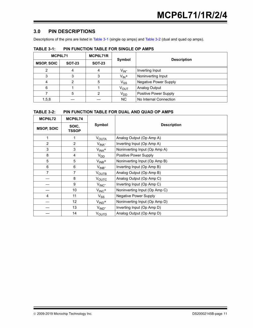
3.0 PIN DESCRIPTIONSDescriptions of the pins are listed in Table 3-1 (single op amps) and Table 3-2 (dual and quad op amps).TABLE 3-1: PIN FUNCTION TABLE FOR SINGLE OP AMPS
TABLE 3-2: PIN FUNCTION TABLE FOR DUAL AND QUAD OP AMPS
MCP6L71 MCP6L71RSymbol Description
MSOP, SOIC SOT-23 SOT-23
2 4 4 VIN- Inverting Input3 3 3 VIN+ Noninverting Input4 2 5 VSS Negative Power Supply6 1 1 VOUT Analog Output7 5 2 VDD Positive Power Supply
1,5,8 — — NC No Internal Connection
MCP6L72 MCP6L74Symbol Description
MSOP, SOIC SOIC, TSSOP
1 1 VOUTA Analog Output (Op Amp A)2 2 VINA- Inverting Input (Op Amp A)3 3 VINA+ Noninverting Input (Op Amp A)8 4 VDD Positive Power Supply5 5 VINB+ Noninverting Input (Op Amp B)6 6 VINB- Inverting Input (Op Amp B)7 7 VOUTB Analog Output (Op Amp B)— 8 VOUTC Analog Output (Op Amp C)— 9 VINC- Inverting Input (Op Amp C)— 10 VINC+ Noninverting Input (Op Amp C)4 11 VSS Negative Power Supply— 12 VIND+ Noninverting Input (Op Amp D)— 13 VIND- Inverting Input (Op Amp D)— 14 VOUTD Analog Output (Op Amp D)
2009-2019 Microchip Technology Inc. DS20002145B-page 11

MCP6L71/1R/2/4
3.1 Analog OutputsThe output pins are low-impedance voltage sources.3.2 Analog InputsThe noninverting and inverting inputs arehigh-impedance CMOS inputs with low bias currents.
3.3 Power Supply PinsThe positive power supply (VDD) is 2.0V to 6.0V higherthan the negative power supply (VSS). For normaloperation, the other pins are at voltages between VSSand VDD.Typically, these parts are used in a single (positive)supply configuration. In this case, VSS is connected toground and VDD is connected to the supply. VDD willneed bypass capacitors.
DS20002145B-page 12 2009-2019 Microchip Technology Inc.

MCP6L71/1R/2/4
4.0 APPLICATION INFORMATIONThe MCP6L71/1R/2/4 family of op amps is manufacturedusing Microchip’s state-of-the-art CMOS process, specifi-cally designed for low-cost, low-power and generalpurpose applications. The low supply voltage, lowquiescent current and wide bandwidth make theMCP6L71/1R/2/4 ideal for battery-powered applications.4.1 Rail-to-Rail Inputs
4.1.1 PHASE REVERSALThe MCP6L71/1R/2/4 op amps are designed to pre-vent phase inversion when the input pins exceed thesupply voltages. Figure 2-10 shows an input voltageexceeding both supplies without any phase reversal.
4.1.2 INPUT VOLTAGE AND CURRENT LIMITS
In order to prevent damage and/or improper operationof these amplifiers, the circuit they are in must limitthe currents (and voltages) at the input pins (seeSection 1.1 “Absolute Maximum Ratings†”).Figure 4-1 shows the recommended approach to pro-tecting these inputs. The internal ESD diodes preventthe input pins (VIN+ and VIN-) from going too far belowground, and the resistors, R1 and R2, limit the possiblecurrent drawn out of the input pins. Diodes, D1 and D2,prevent the input pins (VIN+ and VIN-) from going too farabove VDD, and dump any currents onto VDD.
FIGURE 4-1: Protecting the Analog Inputs.A significant amount of current can flow out of theinputs (through the ESD diodes) when theCommon-mode voltage (VCM) is below ground (VSS);see Figure 2-7. Applications that are high-impedancemay need to limit the usable voltage range.
4.1.3 NORMAL OPERATIONSThe input stage of the MCP6L71/1R/2/4 op amps usestwo differential CMOS input stages in parallel. Oneoperates at low Common-mode input voltage (VCM),while the other at high VCM. With this topology, and atroom temperature, the device operates with VCM up to0.3V above VDD and 0.3V below VSS (typically at +25°C). The transition between the two input stages occurswhen VCM = VDD – 1.1V. For the best distortion andgain linearity, with noninverting gains, avoid this regionof operation.
4.2 Rail-to-Rail OutputThe output voltage range of the MCP6L71/1R/2/4op amps is VDD – 20 mV (minimum), and VSS + 20 mV(maximum) when RL = 10 k is connected to VDD/2 andVDD = 5.0V. Refer to Figure 2-13 for more information.
4.3 Capacitive LoadsDriving large capacitive loads can cause stabilityproblems for voltage feedback op amps. As the loadcapacitance increases, the feedback loop’s phasemargin decreases and the closed-loop bandwidth isreduced. This produces gain peaking in the frequencyresponse, with overshoot and ringing in the stepresponse. When driving large capacitive loads with theseop amps (e.g., > 100 pF when G = +1), a small seriesresistor at the output (RISO in Figure 4-2) improves thefeedback loop’s phase margin (stability) by making theoutput load resistive at higher frequencies. Thebandwidth will be generally lower than the bandwidthwith no capacitive load.
FIGURE 4-2: Output Resistor, RISO Stabilizes Large Capacitive Loads.Bench measurements are helpful in choosing RISO.Adjust RISO so that a small-signal step response (seeFigure 2-15) has reasonable overshoot (e.g., 4%).
V1
MCP6L7XR1
VDD
D1
R1 >VSS – (minimum expected V1)
2 mA
VOUT
R2 >VSS – (minimum expected V2)
2 mA
V2R2
D2
R3
+
–
RISOVOUT
CLMCP6L7X
RFRG
RN
–
+
2009-2019 Microchip Technology Inc. DS20002145B-page 13

MCP6L71/1R/2/4
4.4 Supply BypassWith this family of operational amplifiers, the powersupply pin (VDD for single supply) should have a localbypass capacitor (i.e., 0.01 µF to 0.1 µF) within 2 mmfor good, high-frequency performance. It also needs abulk capacitor (i.e., 1 µF or larger) within 100 mm toprovide large, slow currents. This bulk capacitor can beshared with nearby analog parts.4.5 Unused AmplifiersAn unused op amp in a quad package (MCP6L74)should be configured as shown in Figure 4-3. Thesecircuits prevent the output from toggling and causingcrosstalk. In Circuit A, R1 and R2 produce a voltagewithin its output voltage range (VOH, VOL). The op ampbuffers this voltage, which can be used elsewhere inthe circuit. Circuit B uses the minimum number ofcomponents and operates as a comparator.
FIGURE 4-3: Unused Op Amps.
4.6 PCB Surface LeakageIn applications where low input bias current is critical,Printed Circuit Board (PCB) surface leakage effectsneed to be considered. Surface leakage is caused byhumidity, dust or other contamination on the board.Under low humidity conditions, a typical resistancebetween nearby traces is 1012. A 5V difference wouldcause 5 pA of current to flow. This is greater than theMCP6L71/1R/2/4 family’s bias current at +25°C (1 pA,typical).The easiest way to reduce surface leakage is to use aguard ring around sensitive pins (or traces). The guardring is biased at the same voltage as the sensitive pin.Figure 4-4 shows an example of this type of layout.
FIGURE 4-4: Example Guard Ring Layout.
1. For Inverting Gain and Transimpedance Amplifiers(convert current to voltage, such as photodetectors):a) Connect the guard ring to the noninverting
input pin (VIN+). This biases the guard ringto the same reference voltage as theop amp (e.g., VDD/2 or ground).
b) Connect the inverting pin (VIN-) to the inputwith a wire that does not touch the PCBsurface.
2. Noninverting Gain and Unity Gain Buffer:a) Connect the guard ring to the inverting input
pin (VIN-). This biases the guard ring to theCommon-mode input voltage.
b) Connect the noninverting pin (VIN+) to theinput with a wire that does not touch thePCB surface.
4.7 Application Circuits
4.7.1 INVERTING INTEGRATORAn inverting integrator is shown in Figure 4-5. Thecircuit provides an output voltage that is proportional tothe negative time integral of the input. The additionalresistor R2 limits DC gain and controls output clipping.To minimize the integrator’s error for slow signals, thevalue of R2 should be much larger than the value of R1.
FIGURE 4-5: Inverting Integrator.
¼ MCP6L74 (A)
VDD
¼ MCP6L74 (B)
R1
R2
VDD
VDD
VREF
VREF VDDR2
R1 R2+------------------=
+
–
+
–
Guard Ring VIN- VIN+
+
_C1
R2
VIN
VOUTMCP6L71
R2 R1»
VOUT1
R1C1------------- VIN td
0t–=
R1
DS20002145B-page 14 2009-2019 Microchip Technology Inc.

MCP6L71/1R/2/4
5.0 DESIGN TOOLSMicrochip provides the basic design tools needed forthe MCP6L71/1R/2/4 family of op amps.5.1 FilterLab® SoftwareMicrochip’s FilterLab® software is an innovative softwaretool that simplifies analog active filter (using op amps)design. Available at no cost from the Microchip websiteat www.microchip.com/filterlab, the FilterLab design toolprovides full schematic diagrams of the filter circuit withcomponent values. It also outputs the filter circuit inSPICE format, which can be used with the macro modelto simulate actual filter performance.
5.2 MAPS (Microchip Advanced Part Selector)
MAPS is a software tool that helps efficiently identifyMicrochip devices that fit a particular design require-ment. Available at no cost from the Microchip websiteat www.microchip.com/maps, the MAPS is an overallselection tool for Microchip’s product portfolio thatincludes Analog, Memory, MCUs and DSCs. Using thistool you can define a filter to sort features for aparametric search of devices and export side-by-sidetechnical comparison reports. Helpful links are alsoprovided for data sheets, purchase and sampling ofMicrochip parts.
5.3 Analog Demonstration and Evaluation Boards
Microchip offers a broad spectrum of Analog Demonstra-tion and Evaluation Boards that are designed to help youachieve faster time to market. For a complete listing ofthese boards, and their corresponding user’s guides andtechnical information, visit the Microchip website atwww.microchip.com/analogtools.Some boards that are especially useful are:• MCP6XXX Amplifier Evaluation Board 1• MCP6XXX Amplifier Evaluation Board 2• MCP6XXX Amplifier Evaluation Board 3• MCP6XXX Amplifier Evaluation Board 4• Active Filter Demo Board Kit• 5/6-Pin SOT-23 Evaluation Board, P/N VSUPEV2• 8-Pin SOIC/MSOP/TSSOP/DIP Evaluation Board,
P/N SOIC8EV• 14-Pin SOIC/TSSOP/DIP Evaluation Board,
P/N SOIC14EV
5.4 Application NotesThe following Microchip Application Notes are availableon the Microchip website at www.microchip.com/appnotes and are recommended as supplementalreference resources.• ADN003: “Select the Right Operational Amplifier
for your Filtering Circuits”, DS21821• AN722: “Operational Amplifier Topologies and DC
Specifications”, DS00722• AN723: “Operational Amplifier AC Specifications
and Applications”, DS00723• AN884: “Driving Capacitive Loads With Op Amps”,
DS00884• AN990: “Analog Sensor Conditioning
Circuits – An Overview”, DS00990
2009-2019 Microchip Technology Inc. DS20002145B-page 15

MCP6L71/1R/2/4
NOTES:DS20002145B-page 16 2009-2019 Microchip Technology Inc.
MCP6L71/1R/2/4
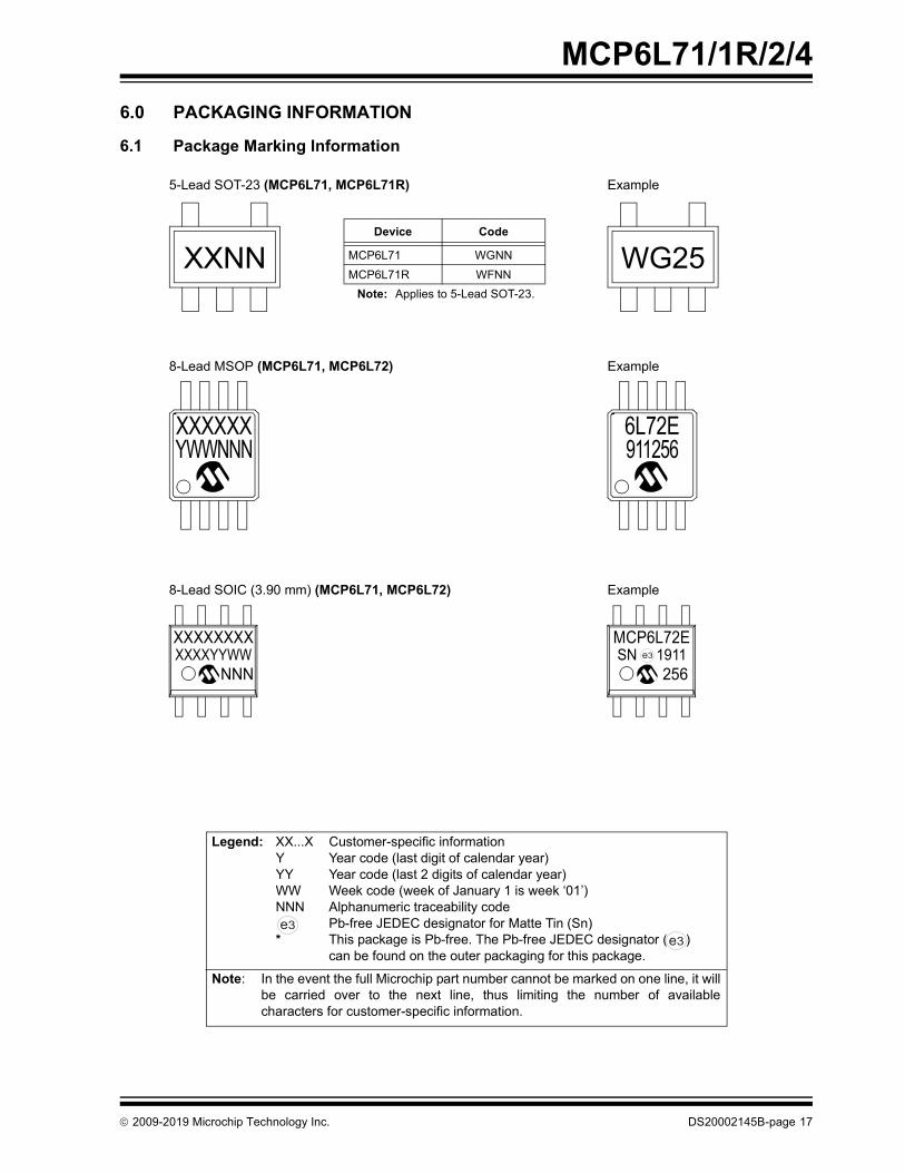
6.0 PACKAGING INFORMATION6.1 Package Marking Information
Device Code
MCP6L71 WGNNMCP6L71R WFNN
Note: Applies to 5-Lead SOT-23.
Legend: XX...X Customer-specific informationY Year code (last digit of calendar year)YY Year code (last 2 digits of calendar year)WW Week code (week of January 1 is week ‘01’)NNN Alphanumeric traceability code Pb-free JEDEC designator for Matte Tin (Sn)* This package is Pb-free. The Pb-free JEDEC designator ( )
can be found on the outer packaging for this package.
Note: In the event the full Microchip part number cannot be marked on one line, it willbe carried over to the next line, thus limiting the number of availablecharacters for customer-specific information.
3e
3e
3e
5-Lead SOT-23 (MCP6L71, MCP6L71R)
XXNN
Example
WG25
XXXXXX
8-Lead MSOP (MCP6L71, MCP6L72)
YWWNNN6L72E
Example
911256
XXXXXXXX
8-Lead SOIC (3.90 mm) (MCP6L71, MCP6L72)
XXXXYYWWNNN
MCP6L72E
Example
SN 1911256
2009-2019 Microchip Technology Inc. DS20002145B-page 17

MCP6L71/1R/2/4
Package Marking Information (Continued)3e
XXXXXXXXXXX
14-Lead SOIC (3.90 mm) (MCP6L74)
XXXXXXXXXXXYYWWNNN
MCP6L74
Example
E/SL1911256
XXXXXXXX
14-Lead TSSOP (4.4 mm) (MCP6L74)
YYWWNNN
6L74EST
Example
1911256
DS20002145B-page 18 2009-2019 Microchip Technology Inc.

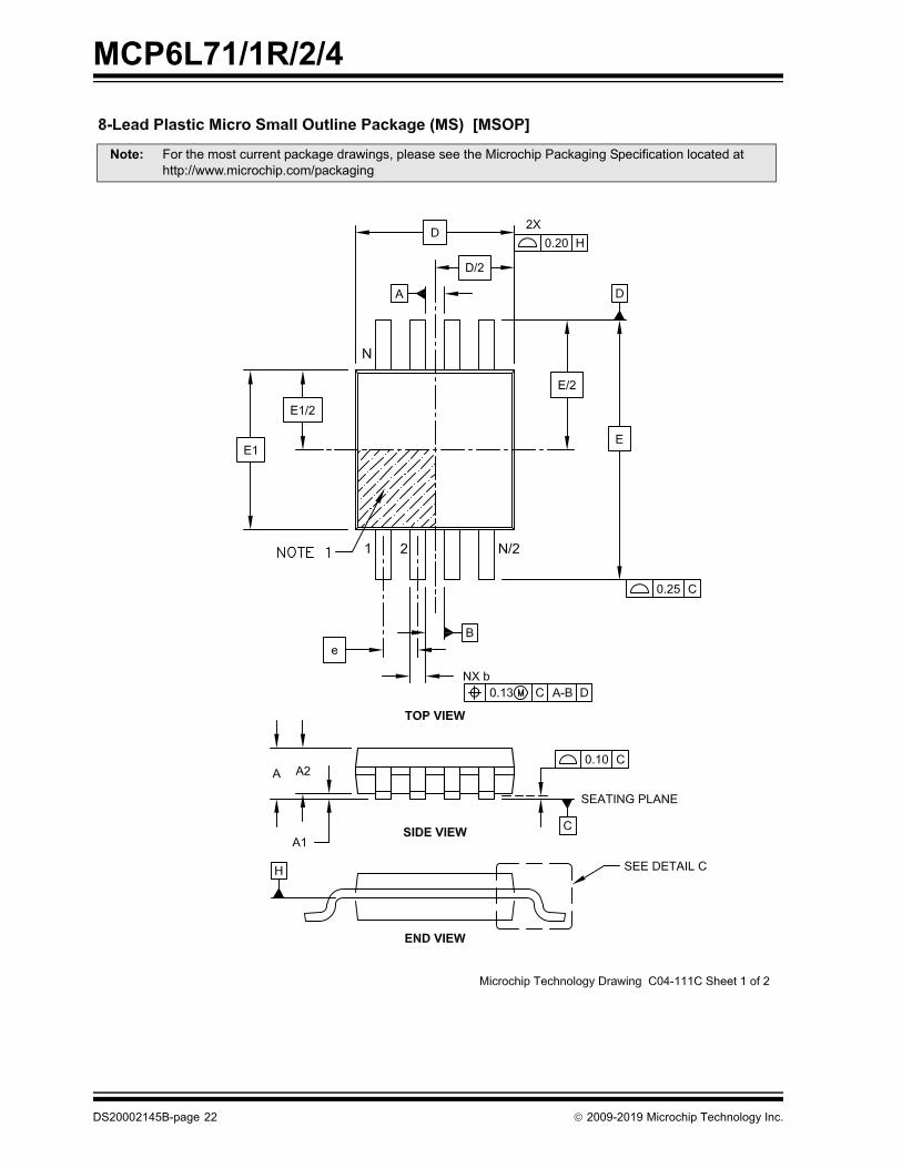
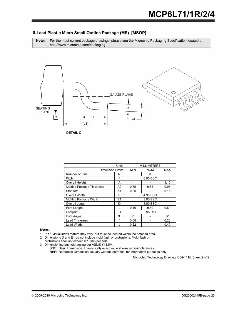
MCP6L71/1R/2/4
0.15 C D2X
NOTE 1 1 2
N
TOP VIEW
SIDE VIEW
Microchip Technology Drawing C04-091-OT Rev F Sheet 1 of 2
For the most current package drawings, please see the Microchip Packaging Specification located athttp://www.microchip.com/packaging
Note:
0.20 C
C
SEATING PLANE
A A2
A1
e
NX bB0.20 C A-B D
e1
D
E1
E1/2
E/2
E
DA
0.20 C 2X
(DATUM D)(DATUM A-B)
A
ASEE SHEET 2
5-Lead Plastic Small Outline Transistor (OT) [SOT23]
2009-2019 Microchip Technology Inc. DS20002145B-page 19

MCP6L71/1R/2/4
Microchip Technology Drawing C04-091-OT Rev F Sheet 2 of 2
For the most current package drawings, please see the Microchip Packaging Specification located athttp://www.microchip.com/packaging
Note:
c
L
L1
VIEW A-ASHEET 1
5-Lead Plastic Small Outline Transistor (OT) [SOT23]
protrusions shall not exceed 0.25mm per side.1.
BSC: Basic Dimension. Theoretically exact value shown without tolerances.2.
Foot Angle
Number of PinsPitchOutside lead pitchOverall HeightMolded Package ThicknessStandoffOverall WidthMolded Package WidthOverall LengthFoot LengthFootprint
Lead ThicknessLead Width
Notes:
L1
bc
Dimension Limits
EE1DL
e1AA2A1
Units
Ne
0°0.080.20 -
--
10°0.260.51
MILLIMETERS
0.95 BSC1.90 BSC
0.30
0.900.89
-
0.60 REF
2.90 BSC-
2.80 BSC1.60 BSC
--
-
MIN5
NOM
1.451.300.15
0.60
MAX
REF: Reference Dimension, usually without tolerance, for information purposes only.
Dimensions D and E1 do not include mold flash or protrusions. Mold flash or
Dimensioning and tolerancing per ASME Y14.5M
DS20002145B-page 20 2009-2019 Microchip Technology Inc.
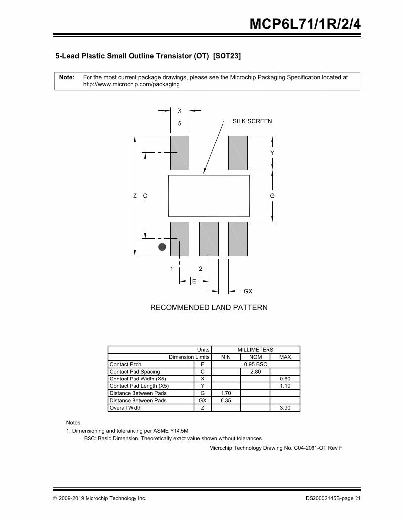
MCP6L71/1R/2/4
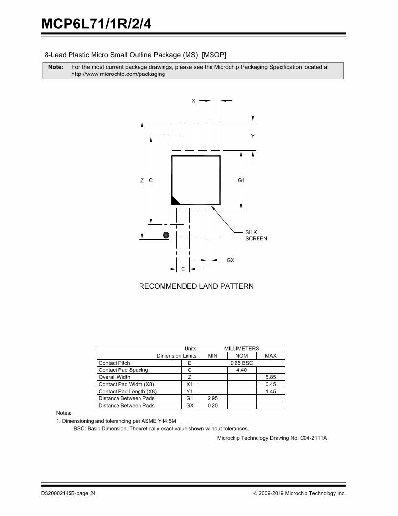
RECOMMENDED LAND PATTERN
5-Lead Plastic Small Outline Transistor (OT) [SOT23]
For the most current package drawings, please see the Microchip Packaging Specification located athttp://www.microchip.com/packaging
Note:
BSC: Basic Dimension. Theoretically exact value shown without tolerances.
Notes:1. Dimensioning and tolerancing per ASME Y14.5M
Microchip Technology Drawing No. C04-2091-OT Rev F
Dimension Limits
Contact Pad Length (X5)
Overall Width
Distance Between Pads
Contact Pad Width (X5)
Contact PitchContact Pad Spacing
3.90
1.10G
Z
Y1.70
0.60
MAXMIN
CX
E
UnitsNOM
0.95 BSC2.80
MILLIMETERS
Distance Between Pads GX 0.35
1
5
X
Y
Z C
E
GX
G
2
SILK SCREEN
2009-2019 Microchip Technology Inc. DS20002145B-page 21
MCP6L71/1R/2/4
Note: For the most current package drawings, please see the Microchip Packaging Specification located at http://www.microchip.com/packaging
DS20002145B-page 22 2009-2019 Microchip Technology Inc.
MCP6L71/1R/2/4
Note: For the most current package drawings, please see the Microchip Packaging Specification located at http://www.microchip.com/packaging
2009-2019 Microchip Technology Inc. DS20002145B-page 23
MCP6L71/1R/2/4
Note: For the most current package drawings, please see the Microchip Packaging Specification located at http://www.microchip.com/packaging
DS20002145B-page 24 2009-2019 Microchip Technology Inc.

MCP6L71/1R/2/4
0.25 C A–B D
CSEATING
PLANE
TOP VIEW
SIDE VIEW
VIEW A–A
0.10 C
0.10 C
Microchip Technology Drawing No. C04-057-SN Rev E Sheet 1 of 2
8X
For the most current package drawings, please see the Microchip Packaging Specification located athttp://www.microchip.com/packaging
Note:
8-Lead Plastic Small Outline (SN) - Narrow, 3.90 mm (.150 In.) Body [SOIC]
1 2
N
h
h
A1
A2A
A
B
e
D
E
E2
E12
E1
NOTE 5
NOTE 5
NX b
0.10 C A–B2X
H 0.23
(L1)L
R0.13
R0.13
VIEW C
SEE VIEW C
NOTE 1
D
2009-2019 Microchip Technology Inc. DS20002145B-page 25
MCP6L71/1R/2/4
Microchip Technology Drawing No. C04-057-SN Rev E Sheet 2 of 2
8-Lead Plastic Small Outline (SN) - Narrow, 3.90 mm (.150 In.) Body [SOIC]
For the most current package drawings, please see the Microchip Packaging Specification located athttp://www.microchip.com/packaging
Note:
Foot Angle 0° - 8°
15°-5°Mold Draft Angle Bottom15°-5°Mold Draft Angle Top0.51-0.31bLead Width0.25-0.17cLead Thickness
1.27-0.40LFoot Length0.50-0.25hChamfer (Optional)
4.90 BSCDOverall Length3.90 BSCE1Molded Package Width6.00 BSCEOverall Width
0.25-0.10A1Standoff--1.25A2Molded Package Thickness
1.75--AOverall Height1.27 BSCePitch
8NNumber of PinsMAXNOMMINDimension Limits
MILLIMETERSUnits
protrusions shall not exceed 0.15mm per side.3. Dimensions D and E1 do not include mold flash or protrusions. Mold flash or
REF: Reference Dimension, usually without tolerance, for information purposes only.BSC: Basic Dimension. Theoretically exact value shown without tolerances.
1. Pin 1 visual index feature may vary, but must be located within the hatched area.2. § Significant Characteristic
4. Dimensioning and tolerancing per ASME Y14.5M
Notes:
§
Footprint L1 1.04 REF
5. Datums A & B to be determined at Datum H.
DS20002145B-page 26 2009-2019 Microchip Technology Inc.

MCP6L71/1R/2/4
RECOMMENDED LAND PATTERN
Microchip Technology Drawing C04-2057-SN Rev E
8-Lead Plastic Small Outline (SN) - Narrow, 3.90 mm Body [SOIC]
BSC: Basic Dimension. Theoretically exact value shown without tolerances.
Notes:Dimensioning and tolerancing per ASME Y14.5M1.
For the most current package drawings, please see the Microchip Packaging Specification located athttp://www.microchip.com/packaging
Note:
Dimension LimitsUnits
CContact Pad SpacingContact Pitch
MILLIMETERS
1.27 BSCMIN
EMAX
5.40
Contact Pad Length (X8)Contact Pad Width (X8)
Y1X1
1.550.60
NOM
E
X1
C
Y1
SILK SCREEN
2009-2019 Microchip Technology Inc. DS20002145B-page 27

MCP6L71/1R/2/4
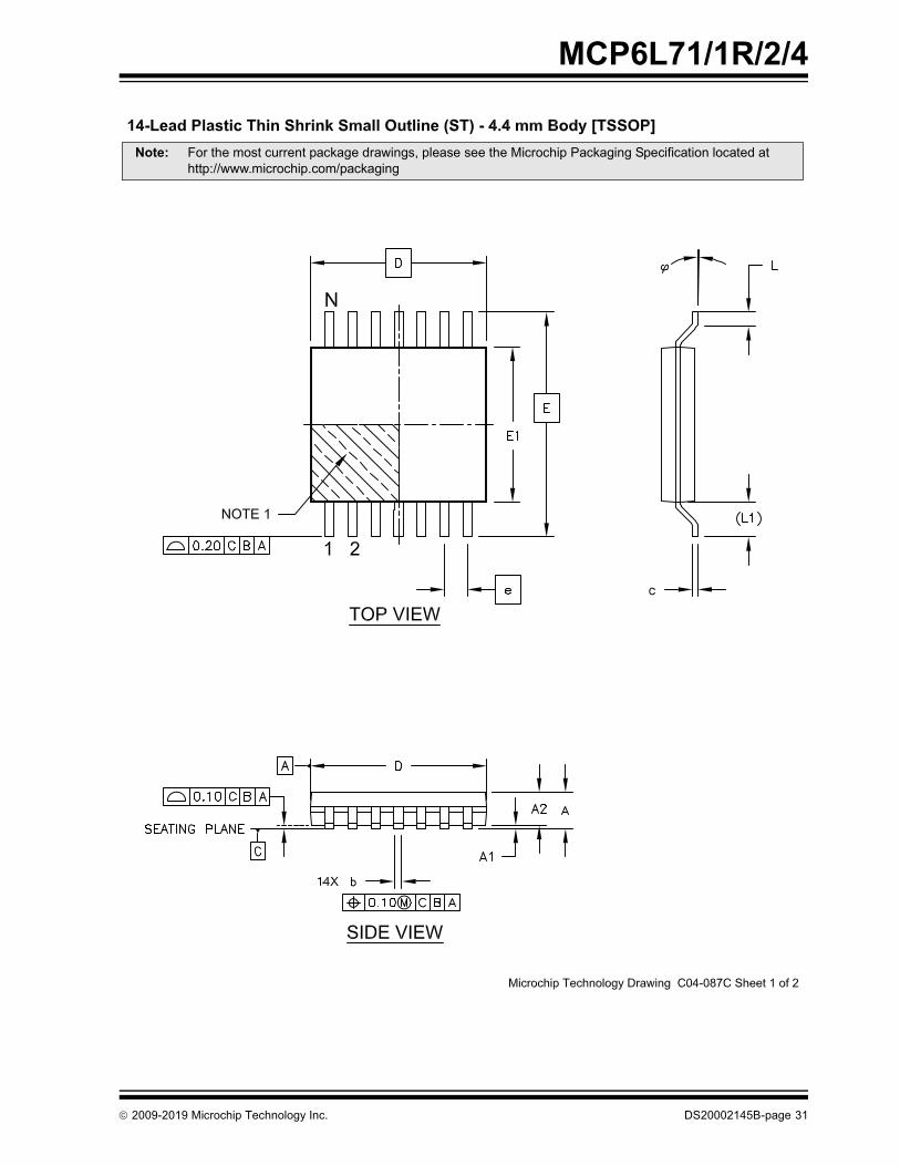
Microchip Technology Drawing No. C04-065-SL Rev D Sheet 1 of 2
For the most current package drawings, please see the Microchip Packaging Specification located athttp://www.microchip.com/packaging
Note:
14-Lead Plastic Small Outline (SL) - Narrow, 3.90 mm Body [SOIC]
0.20 C
0.25 C A–B D
1 2
N
2X N/2 TIPS
TOP VIEW
SIDE VIEW
VIEW A–A
A
e
B
E
D
E2
D
E1
E22
NX b
A1
A2ACSEATING
PLANE
0.10 C14X
0.10 C A–B
0.10 C D
c
hh
H
SEE VIEW C
(L1)L
R0.13R0.13
VIEW C
NOTE 1 3
0.10 C
NOTE 5
NOTE 5
2X
2X
DS20002145B-page 28 2009-2019 Microchip Technology Inc.

MCP6L71/1R/2/4
Microchip Technology Drawing No. C04-065-SL Rev D Sheet 2 of 2
14-Lead Plastic Small Outline (SL) - Narrow, 3.90 mm Body [SOIC]
For the most current package drawings, please see the Microchip Packaging Specification located athttp://www.microchip.com/packaging
Note:
Foot Angle 0° - 8°
15°-5°Mold Draft Angle Bottom15°-5°Mold Draft Angle Top0.51-0.31bLead Width0.25-0.10cLead Thickness
1.04 REFL1Footprint
0.50-0.25hChamfer (Optional)8.65 BSCDOverall Length3.90 BSCE1Molded Package Width6.00 BSCEOverall Width
0.25-0.10A1Standoff--1.25A2Molded Package Thickness
1.75--AOverall Height1.27 BSCePitch
14NNumber of PinsMAXNOMMINDimension Limits
MILLIMETERSUnits
Foot Length L 0.40 - 1.27
§
or protrusion, which shall not exceed 0.25 mm per side.
3.
REF: Reference Dimension, usually without tolerance, for information purposes only.BSC: Basic Dimension. Theoretically exact value shown without tolerances.
1.2.
4.
Notes:
Dimension D does not include mold flash, protrusions or gate burrs, which shall
Pin 1 visual index feature may vary, but must be located within the hatched area.§ Significant Characteristic
Dimensioning and tolerancing per ASME Y14.5M
not exceed 0.15 mm per end. Dimension E1 does not include interlead flash
5. Datums A & B to be determined at Datum H.
Lead Angle 0° - -
2009-2019 Microchip Technology Inc. DS20002145B-page 29

MCP6L71/1R/2/4
RECOMMENDED LAND PATTERN
Dimension LimitsUnits
Contact Pitch
MILLIMETERS
1.27 BSCMIN
EMAX
Contact Pad Length (X14)Contact Pad Width (X14)
YX
1.550.60
NOM
CContact Pad Spacing 5.40
BSC: Basic Dimension. Theoretically exact value shown without tolerances.
Notes:Dimensioning and tolerancing per ASME Y14.5M1.
For the most current package drawings, please see the Microchip Packaging Specification located athttp://www.microchip.com/packaging
Note:
E
X
Y
C
SILK SCREEN
Microchip Technology Drawing No. C04-2065-SL Rev D
14-Lead Plastic Small Outline (SL) - Narrow, 3.90 mm Body [SOIC]
1 2
14
DS20002145B-page 30 2009-2019 Microchip Technology Inc.
MCP6L71/1R/2/4
Note: For the most current package drawings, please see the Microchip Packaging Specification located at http://www.microchip.com/packaging
2009-2019 Microchip Technology Inc. DS20002145B-page 31

MCP6L71/1R/2/4
Note: For the most current package drawings, please see the Microchip Packaging Specification located at http://www.microchip.com/packaging
DS20002145B-page 32 2009-2019 Microchip Technology Inc.

MCP6L71/1R/2/4
Note: For the most current package drawings, please see the Microchip Packaging Specification located at http://www.microchip.com/packaging
2009-2019 Microchip Technology Inc. DS20002145B-page 33

MCP6L71/1R/2/4
NOTES:DS20002145B-page 34 2009-2019 Microchip Technology Inc.

MCP6L71/1R/2/4
APPENDIX A: REVISION HISTORYRevision B (October 2019)The following is the list of modifications:1. Updated Section 6.0 “Packaging
Information”.
Revision A (March 2009)• Original data sheet release.
2009-2019 Microchip Technology Inc. DS20002145B-page 35

MCP6L71/1R/2/4
NOTES:DS20002145B-page 36 2009-2019 Microchip Technology Inc.
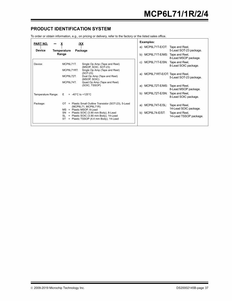
MCP6L71/1R/2/4
PRODUCT IDENTIFICATION SYSTEMTo order or obtain information, e.g., on pricing or delivery, refer to the factory or the listed sales office.Device: MCP6L71T: Single Op Amp (Tape and Reel)
(MSOP, SOIC, SOT-23)MCP6L71RT: Single Op Amp (Tape and Reel)
(SOT-23)MCP6L72T: Dual Op Amp (Tape and Reel)
(MSOP, SOIC)MCP6L74T: Quad Op Amp (Tape and Reel)
(SOIC, TSSOP)
Temperature Range: E = -40°C to +125°C
Package: OT = Plastic Small Outline Transistor (SOT-23), 5-Lead(MCP6L71, MCP6L71R)
MS = Plastic MSOP, 8-LeadSN = Plastic SOIC (3.90 mm Body), 8-LeadSL = Plastic SOIC (3.90 mm Body), 14-LeadST = Plastic TSSOP (4.4 mm Body), 14-Lead
PART NO. X /XX
PackageTemperatureRange
Device
Examples:a) MCP6L71T-E/OT: Tape and Reel,
5-Lead SOT-23 package.b) MCP6L71T-E/MS: Tape and Reel,
8-Lead MSOP package.c) MCP6L71T-E/SN: Tape and Reel,
8-Lead SOIC package.
a) MCP6L71RT-E/OT: Tape and Reel, 5-Lead SOT-23 package.
a) MCP6L72T-E/MS: Tape and Reel, 8-Lead MSOP package.
b) MCP6L72T-E/SN: Tape and Reel,8-Lead SOIC package.
a) MCP6L74T-E/SL: Tape and Reel,14-Lead SOIC package.
b) MCP6L74-E/ST: Tape and Reel,14-Lead TSSOP package.
–
2009-2019 Microchip Technology Inc. DS20002145B-page 37

MCP6L71/1R/2/4
NOTES:DS20002145B-page 38 2009-2019 Microchip Technology Inc.
Note the following details of the code protection feature on Microchip devices:• Microchip products meet the specification contained in their particular Microchip Data Sheet.
• Microchip believes that its family of products is one of the most secure families of its kind on the market today, when used in the intended manner and under normal conditions.
• There are dishonest and possibly illegal methods used to breach the code protection feature. All of these methods, to our knowledge, require using the Microchip products in a manner outside the operating specifications contained in Microchip’s Data Sheets. Most likely, the person doing so is engaged in theft of intellectual property.
• Microchip is willing to work with the customer who is concerned about the integrity of their code.
• Neither Microchip nor any other semiconductor manufacturer can guarantee the security of their code. Code protection does not mean that we are guaranteeing the product as “unbreakable.”
Code protection is constantly evolving. We at Microchip are committed to continuously improving the code protection features of ourproducts. Attempts to break Microchip’s code protection feature may be a violation of the Digital Millennium Copyright Act. If such actsallow unauthorized access to your software or other copyrighted work, you may have a right to sue for relief under that Act.
Information contained in this publication regarding deviceapplications and the like is provided only for your convenienceand may be superseded by updates. It is your responsibility toensure that your application meets with your specifications.MICROCHIP MAKES NO REPRESENTATIONS ORWARRANTIES OF ANY KIND WHETHER EXPRESS ORIMPLIED, WRITTEN OR ORAL, STATUTORY OROTHERWISE, RELATED TO THE INFORMATION,INCLUDING BUT NOT LIMITED TO ITS CONDITION,QUALITY, PERFORMANCE, MERCHANTABILITY ORFITNESS FOR PURPOSE. Microchip disclaims all liabilityarising from this information and its use. Use of Microchipdevices in life support and/or safety applications is entirely atthe buyer’s risk, and the buyer agrees to defend, indemnify andhold harmless Microchip from any and all damages, claims,suits, or expenses resulting from such use. No licenses areconveyed, implicitly or otherwise, under any Microchipintellectual property rights unless otherwise stated.
2009-2019 Microchip Technology Inc.
For information regarding Microchip’s Quality Management Systems, please visit www.microchip.com/quality.
TrademarksThe Microchip name and logo, the Microchip logo, Adaptec, AnyRate, AVR, AVR logo, AVR Freaks, BesTime, BitCloud, chipKIT, chipKIT logo, CryptoMemory, CryptoRF, dsPIC, FlashFlex, flexPWR, HELDO, IGLOO, JukeBlox, KeeLoq, Kleer, LANCheck, LinkMD, maXStylus, maXTouch, MediaLB, megaAVR, Microsemi, Microsemi logo, MOST, MOST logo, MPLAB, OptoLyzer, PackeTime, PIC, picoPower, PICSTART, PIC32 logo, PolarFire, Prochip Designer, QTouch, SAM-BA, SenGenuity, SpyNIC, SST, SST Logo, SuperFlash, Symmetricom, SyncServer, Tachyon, TempTrackr, TimeSource, tinyAVR, UNI/O, Vectron, and XMEGA are registered trademarks of Microchip Technology Incorporated in the U.S.A. and other countries.
APT, ClockWorks, The Embedded Control Solutions Company, EtherSynch, FlashTec, Hyper Speed Control, HyperLight Load, IntelliMOS, Libero, motorBench, mTouch, Powermite 3, Precision Edge, ProASIC, ProASIC Plus, ProASIC Plus logo, Quiet-Wire, SmartFusion, SyncWorld, Temux, TimeCesium, TimeHub, TimePictra, TimeProvider, Vite, WinPath, and ZL are registered trademarks of Microchip Technology Incorporated in the U.S.A.
Adjacent Key Suppression, AKS, Analog-for-the-Digital Age, Any Capacitor, AnyIn, AnyOut, BlueSky, BodyCom, CodeGuard, CryptoAuthentication, CryptoAutomotive, CryptoCompanion, CryptoController, dsPICDEM, dsPICDEM.net, Dynamic Average Matching, DAM, ECAN, EtherGREEN, In-Circuit Serial Programming, ICSP, INICnet, Inter-Chip Connectivity, JitterBlocker, KleerNet, KleerNet logo, memBrain, Mindi, MiWi, MPASM, MPF, MPLAB Certified logo, MPLIB, MPLINK, MultiTRAK, NetDetach, Omniscient Code Generation, PICDEM, PICDEM.net, PICkit, PICtail, PowerSmart, PureSilicon, QMatrix, REAL ICE, Ripple Blocker, SAM-ICE, Serial Quad I/O, SMART-I.S., SQI, SuperSwitcher, SuperSwitcher II, Total Endurance, TSHARC, USBCheck, VariSense, ViewSpan, WiperLock, Wireless DNA, and ZENA are trademarks of Microchip Technology Incorporated in the U.S.A. and other countries.
SQTP is a service mark of Microchip Technology Incorporated in the U.S.A.The Adaptec logo, Frequency on Demand, Silicon Storage Technology, and Symmcom are registered trademarks of Microchip Technology Inc. in other countries.GestIC is a registered trademark of Microchip Technology Germany II GmbH & Co. KG, a subsidiary of Microchip Technology Inc., in other countries. All other trademarks mentioned herein are property of their respective companies.
© 2009-2019, Microchip Technology Incorporated, All Rights Reserved.
ISBN: 978-1-5224-5292-8
DS20002145B-page 39
DS20002145B-page 40 2009-2019 Microchip Technology Inc.
AMERICASCorporate Office2355 West Chandler Blvd.Chandler, AZ 85224-6199Tel: 480-792-7200 Fax: 480-792-7277Technical Support: http://www.microchip.com/supportWeb Address: www.microchip.comAtlantaDuluth, GA Tel: 678-957-9614 Fax: 678-957-1455Austin, TXTel: 512-257-3370 BostonWestborough, MA Tel: 774-760-0087 Fax: 774-760-0088ChicagoItasca, IL Tel: 630-285-0071 Fax: 630-285-0075DallasAddison, TX Tel: 972-818-7423 Fax: 972-818-2924DetroitNovi, MI Tel: 248-848-4000Houston, TX Tel: 281-894-5983IndianapolisNoblesville, IN Tel: 317-773-8323Fax: 317-773-5453Tel: 317-536-2380Los AngelesMission Viejo, CA Tel: 949-462-9523Fax: 949-462-9608Tel: 951-273-7800 Raleigh, NC Tel: 919-844-7510New York, NY Tel: 631-435-6000San Jose, CA Tel: 408-735-9110Tel: 408-436-4270Canada - TorontoTel: 905-695-1980 Fax: 905-695-2078
ASIA/PACIFICAustralia - SydneyTel: 61-2-9868-6733China - BeijingTel: 86-10-8569-7000 China - ChengduTel: 86-28-8665-5511China - ChongqingTel: 86-23-8980-9588China - DongguanTel: 86-769-8702-9880 China - GuangzhouTel: 86-20-8755-8029 China - HangzhouTel: 86-571-8792-8115 China - Hong Kong SARTel: 852-2943-5100 China - NanjingTel: 86-25-8473-2460China - QingdaoTel: 86-532-8502-7355China - ShanghaiTel: 86-21-3326-8000 China - ShenyangTel: 86-24-2334-2829China - ShenzhenTel: 86-755-8864-2200 China - SuzhouTel: 86-186-6233-1526 China - WuhanTel: 86-27-5980-5300China - XianTel: 86-29-8833-7252China - XiamenTel: 86-592-2388138 China - ZhuhaiTel: 86-756-3210040
ASIA/PACIFICIndia - BangaloreTel: 91-80-3090-4444 India - New DelhiTel: 91-11-4160-8631India - PuneTel: 91-20-4121-0141Japan - OsakaTel: 81-6-6152-7160 Japan - TokyoTel: 81-3-6880- 3770 Korea - DaeguTel: 82-53-744-4301Korea - SeoulTel: 82-2-554-7200Malaysia - Kuala LumpurTel: 60-3-7651-7906Malaysia - PenangTel: 60-4-227-8870Philippines - ManilaTel: 63-2-634-9065SingaporeTel: 65-6334-8870Taiwan - Hsin ChuTel: 886-3-577-8366Taiwan - KaohsiungTel: 886-7-213-7830Taiwan - TaipeiTel: 886-2-2508-8600 Thailand - BangkokTel: 66-2-694-1351Vietnam - Ho Chi MinhTel: 84-28-5448-2100
EUROPEAustria - WelsTel: 43-7242-2244-39Fax: 43-7242-2244-393Denmark - CopenhagenTel: 45-4450-2828 Fax: 45-4485-2829Finland - EspooTel: 358-9-4520-820France - ParisTel: 33-1-69-53-63-20 Fax: 33-1-69-30-90-79 Germany - GarchingTel: 49-8931-9700Germany - HaanTel: 49-2129-3766400Germany - HeilbronnTel: 49-7131-72400Germany - KarlsruheTel: 49-721-625370Germany - MunichTel: 49-89-627-144-0 Fax: 49-89-627-144-44Germany - RosenheimTel: 49-8031-354-560Israel - Ra’anana Tel: 972-9-744-7705Italy - Milan Tel: 39-0331-742611 Fax: 39-0331-466781Italy - PadovaTel: 39-049-7625286 Netherlands - DrunenTel: 31-416-690399 Fax: 31-416-690340Norway - TrondheimTel: 47-7288-4388Poland - WarsawTel: 48-22-3325737 Romania - BucharestTel: 40-21-407-87-50Spain - MadridTel: 34-91-708-08-90Fax: 34-91-708-08-91Sweden - GothenbergTel: 46-31-704-60-40Sweden - StockholmTel: 46-8-5090-4654UK - WokinghamTel: 44-118-921-5800Fax: 44-118-921-5820
Worldwide Sales and Service
05/14/19