Embed Size (px)
Citation preview
ADS1210ADS1211
24-Bit ANALOG-TO-DIGITAL CONVERTER
FEATURES DELTA-SIGMA A/D CONVERTER
23 BITS EFFECTIVE RESOLUTION AT 10HzAND 20 BITS AT 1000Hz
DIFFERENTIAL INPUTS
PROGRAMMABLE GAIN AMPLIFIER
FLEXIBLE SPI™-COMPATIBLE SSIINTERFACE WITH 2-WIRE MODE
PROGRAMMABLE CUT-OFF FREQUENCYUP TO 15.6kHz
INTERNAL/EXTERNAL REFERENCE
ON-CHIP SELF-CALIBRATION
ADS1211 INCLUDES 4-CHANNEL MUX
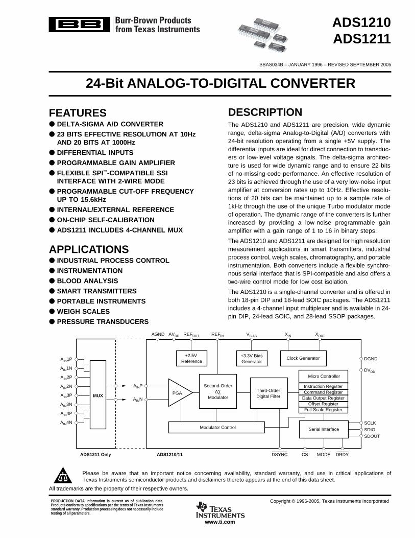
DESCRIPTIONThe ADS1210 and ADS1211 are precision, wide dynamicrange, delta-sigma Analog-to-Digital (A/D) converters with24-bit resolution operating from a single +5V supply. Thedifferential inputs are ideal for direct connection to transduc-ers or low-level voltage signals. The delta-sigma architec-ture is used for wide dynamic range and to ensure 22 bitsof no-missing-code performance. An effective resolution of23 bits is achieved through the use of a very low-noise inputamplifier at conversion rates up to 10Hz. Effective resolu-tions of 20 bits can be maintained up to a sample rate of1kHz through the use of the unique Turbo modulator modeof operation. The dynamic range of the converters is furtherincreased by providing a low-noise programmable gainamplifier with a gain range of 1 to 16 in binary steps.
The ADS1210 and ADS1211 are designed for high resolutionmeasurement applications in smart transmitters, industrialprocess control, weigh scales, chromatography, and portableinstrumentation. Both converters include a flexible synchro-nous serial interface that is SPI-compatible and also offers atwo-wire control mode for low cost isolation.
The ADS1210 is a single-channel converter and is offered inboth 18-pin DIP and 18-lead SOIC packages. The ADS1211includes a 4-channel input multiplexer and is available in 24-pin DIP, 24-lead SOIC, and 28-lead SSOP packages.
APPLICATIONS INDUSTRIAL PROCESS CONTROL
INSTRUMENTATION
BLOOD ANALYSIS
SMART TRANSMITTERS
PORTABLE INSTRUMENTS
WEIGH SCALES
PRESSURE TRANSDUCERS
ADS1210
ADS1211
ADS1210
ADS1211ADS1211
PGA
+2.5V Reference
+3.3V BiasGenerator
Clock Generator
Serial Interface
Second-Order∆∑
Modulator
Instruction RegisterCommand Register
Data Output RegisterOffset Register
Full-Scale Register
Third-OrderDigital Filter
Micro Controller
Modulator Control
AGND AVDD REFOUT REFIN VBIAS XIN XOUT
MODEDSYNCADS1211 Only ADS1210/11 CS DRDY
AINP
AINN
SCLK
DGND
DVDD
SDIOSDOUT
MUX
AIN1P
AIN1N
AIN2P
AIN2N
AIN3P
AIN3N
AIN4P
AIN4N
SBAS034B – JANUARY 1996 – REVISED SEPTEMBER 2005
www.ti.com
PRODUCTION DATA information is current as of publication date.Products conform to specifications per the terms of Texas Instrumentsstandard warranty. Production processing does not necessarily includetesting of all parameters.
Copyright © 1996-2005, Texas Instruments Incorporated
Please be aware that an important notice concerning availability, standard warranty, and use in critical applications ofTexas Instruments semiconductor products and disclaimers thereto appears at the end of this data sheet.
All trademarks are the property of their respective owners.
ADS1210, ADS12112SBAS034Bwww.ti.com
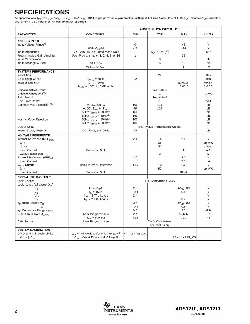
All specifications TMIN to TMAX, AVDD = DVDD = +5V, fXIN = 10MHz, programmable gain amplifier setting of 1, Turbo Mode Rate of 1, REFOUT disabled,VBIAS disabled,and external 2.5V reference, unless otherwise specified.
SPECIFICATIONS
ADS1210U, P/ADS1211U, P, E
PARAMETER CONDITIONS MIN TYP MAX UNITS
ANALOG INPUTInput Voltage Range(1) 0 +5 V
With VBIAS(2) –10 +10 V
Input Impedance G = Gain, TMR = Turbo Mode Rate 4/(G • TMR)(3) MΩProgrammable Gain Amplifier User Programmable: 1, 2, 4, 8, or 16 1 16Input Capacitance 8 pFInput Leakage Current At +25°C 5 50 pA
At TMIN to TMAX 1 nA
SYSTEMS PERFORMANCEResolution 24 BitsNo Missing Codes fDATA = 60Hz 22 BitsIntegral Linearity fDATA = 60Hz ±0.0015 %FSR
fDATA = 1000Hz, TMR of 16 ±0.0015 %FSRUnipolar Offset Error(4) See Note 5Unipolar Offset Drift(6) 1 µV/°CGain Error(4) See Note 5Gain Error Drift(6) 1 µV/°CCommon-Mode Rejection(9) At DC, +25°C 100 115 dB
At DC, TMIN to TMAX 90 115 dB50Hz, fDATA = 50Hz(7) 160 dB60Hz, fDATA = 60Hz(7) 160 dB
Normal-Mode Rejection 50Hz, fDATA = 50Hz(7) 100 dB60Hz, fDATA = 60Hz(7) 100 dB
Output Noise See Typical Performance CurvesPower Supply Rejection DC, 50Hz, and 60Hz 65 dB
VOLTAGE REFERENCEInternal Reference (REFOUT) 2.4 2.5 2.6 V
Drift 25 ppm/°CNoise 50 µVp-pLoad Current Source or Sink 1 mAOutput Impedance 2 Ω
External Reference (REFIN) 2.0 3.0 VLoad Current 2.5 µA
VBIAS Output Using Internal Reference 3.15 3.3 3.45 VDrift 50 ppm/°CLoad Current Source or Sink 10mA
DIGITAL INPUT/OUTPUTLogic Family TTL Compatible CMOSLogic Level: (all except XIN)
VIH IIH = +5µA 2.0 DVDD +0.3 VVIL IIL = +5µA –0.3 0.8 VVOH IOH = 2 TTL Loads 2.4 VVOL IOL = 2 TTL Loads 0.4 V
XIN Input Levels: VIH 3.5 DVDD +0.3 VVIL –0.3 0.8 V
XIN Frequency Range (fXIN) 0.5 10 MHzOutput Data Rate (fDATA) User Programmable 2.4 15,625 Hz
fXIN = 500kHz 0.12 781 HzData Format User Programmable Two’s Complement
or Offset Binary
SYSTEM CALIBRATIONOffset and Full-Scale Limits VFS = Full-Scale Differential Voltage(8) 0.7 • (2 • REFIN)/G
VFS – | VOS | VOS = Offset Differential Voltage(8) 1.3 • (2 • REFIN)/G
ADS1210, ADS1211 3SBAS034B www.ti.com
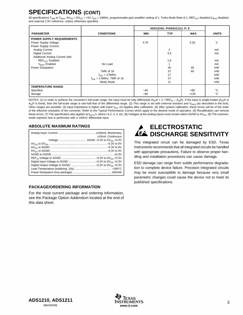
POWER SUPPLY REQUIREMENTSPower Supply Voltage 4.75 5.25 VPower Supply Current:
Analog Current 2 mADigital Current 3.5 mAAdditional Analog Current with
REFOUT Enabled 1.6 mAVBIAS Enabled No Load 1 mA
Power Dissipation 26 40 mWTMR of 16 37 60 mW
fXIN = 2.5MHz 17 mWfXIN = 2.5MHz, TMR of 16 27 mW
Sleep Mode 11 mW
TEMPERATURE RANGESpecified –40 +85 °CStorage –60 +125 °C
NOTES: (1) In order to achieve the converter’s full-scale range, the input must be fully differential (AINN = 2 • REFIN – AINP). If the input is single-ended (AINN orAINP is fixed), then the full-scale range is one-half that of the differential range. (2) This range is set with external resistors and VBIAS (as described in the text).Other ranges are possible. (3) Input impedance is higher with lower fXIN. (4) Applies after calibration. (5) After system calibration, these errors will be of the orderof the effective resolution of the converter. Refer to the Typical Performance Curves which apply to the desired mode of operation. (6) Recalibration can removethese errors. (7) The specification also applies at fDATA /i, where i is 2, 3, 4, etc. (8) Voltages at the analog inputs must remain within AGND to AVDD. (9) The common-mode rejection test is performed with a 100mV differential input.
SPECIFICATIONS (CONT)
ADS1210U, P/ADS1211U, P, E
PARAMETER CONDITIONS MIN TYP MAX UNITS
PACKAGE/ORDERING INFORMATION
For the most current package and ordering information,see the Package Option Addendum located at the end ofthis data sheet.
Analog Input: Current ................................................ ±100mA, Momentary±10mA, Continuous
Voltage ................................... AGND –0.3V to AVDD +0.3VAVDD to DVDD ........................................................................... –0.3V to 6VAVDD to AGND ......................................................................... –0.3V to 6VDVDD to DGND ......................................................................... –0.3V to 6VAGND to DGND ................................................................................ ±0.3VREFIN Voltage to AGND ............................................ –0.3V to AVDD +0.3VDigital Input Voltage to DGND .................................. –0.3V to DVDD +0.3VDigital Output Voltage to DGND ............................... –0.3V to DVDD +0.3VLead Temperature (soldering, 10s) .............................................. +300°CPower Dissipation (Any package) .................................................. 500mW
ABSOLUTE MAXIMUM RATINGS
All specifications TMIN to TMAX, AVDD = DVDD = +5V, fXIN = 10MHz, programmable gain amplifier setting of 1, Turbo Mode Rate of 1, REFOUT disabled,VBIAS disabled,and external 2.5V reference, unless otherwise specified.
ELECTROSTATICDISCHARGE SENSITIVITY
This integrated circuit can be damaged by ESD. TexasInstruments recommends that all integrated circuits be handledwith appropriate precautions. Failure to observe proper han-dling and installation procedures can cause damage.
ESD damage can range from subtle performance degrada-tion to complete device failure. Precision integrated circuitsmay be more susceptible to damage because very smallparametric changes could cause the device not to meet itspublished specifications.
ADS1210, ADS12114SBAS034Bwww.ti.com
PGA
+2.5VReference
+3.3V BiasGenerator
Clock Generator
Serial Interface
Second-Order∆Σ
Modulator
Instruction RegisterCommand Register
Data Output RegisterOffset Register
Full-Scale Register
Third-OrderDigital Filter
Micro Controller
Modulator Control
11
9
10
1213
AGND AVDD REF OUT REF IN VBIAS XIN XOUT
3
1
2
16 17 18 4 7 8
6 5 1415
DSYNC CS DRDYMODE
AINP
AINN
SCLK
DGND
DVDD
SDIOSDOUT
ADS1210
1
2
3
4
5
6
7
8
9
18
17
16
15
14
13
12
11
10
AINP
AINN
AGND
VBIAS
CS
DSYNC
XIN
XOUT
DGND
REFIN
REFOUT
AVDD
MODE
DRDY
SDOUT
SDIO
SCLK
DVDD
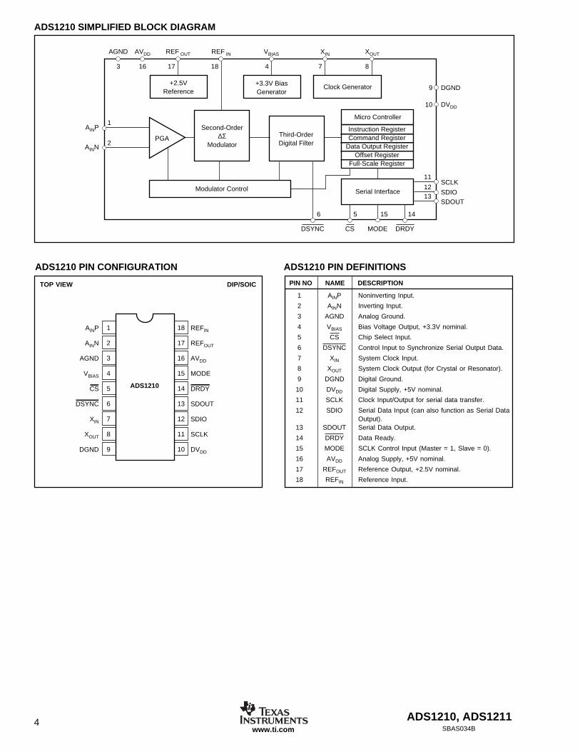
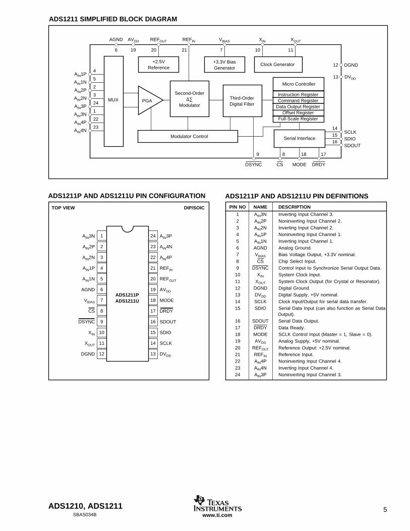
ADS1210 SIMPLIFIED BLOCK DIAGRAM
ADS1210 PIN DEFINITIONS
PIN NO NAME DESCRIPTION
1 AINP Noninverting Input.
2 AINN Inverting Input.
3 AGND Analog Ground.
4 VBIAS Bias Voltage Output, +3.3V nominal.
5 CS Chip Select Input.
6 DSYNC Control Input to Synchronize Serial Output Data.
7 XIN System Clock Input.
8 XOUT System Clock Output (for Crystal or Resonator).
9 DGND Digital Ground.
10 DVDD Digital Supply, +5V nominal.
11 SCLK Clock Input/Output for serial data transfer.
12 SDIO Serial Data Input (can also function as Serial DataOutput).
13 SDOUT Serial Data Output.
14 DRDY Data Ready.
15 MODE SCLK Control Input (Master = 1, Slave = 0).
16 AVDD Analog Supply, +5V nominal.
17 REFOUT Reference Output, +2.5V nominal.
18 REFIN Reference Input.
TOP VIEW DIP/SOIC
ADS1210 PIN CONFIGURATION
ADS1210, ADS1211 5SBAS034B www.ti.com
PGA
+2.5VReference
+3.3V BiasGenerator
Clock Generator
Serial Interface
Second-Order∆∑
Modulator
Third-OrderDigital Filter
Modulator Control
14
12
13
1516
AGND AVDD REFOUT REFIN VBIAS XIN XOUT
6 19 20 21 7 10 11
9 8 1718
DSYNC CS DRDYMODE
SCLK
DGND
DVDD
SDIOSDOUT
4
5
2
3
24
1
22
23
MUX
AIN1P
AIN1N
AIN2P
AIN2N
AIN3P
AIN3N
AIN4P
AIN4N
Instruction RegisterCommand Register
Data Output RegisterOffset Register
Full-Scale Register
Micro Controller
ADS1211 SIMPLIFIED BLOCK DIAGRAM
ADS1211P AND ADS1211U PIN DEFINITIONS
TOP VIEW DIP/SOIC
ADS1211P AND ADS1211U PIN CONFIGURATION
PIN NO NAME DESCRIPTION
1 AIN3N Inverting Input Channel 3.2 AIN2P Noninverting Input Channel 2.3 AIN2N Inverting Input Channel 2.4 AIN1P Noninverting Input Channel 1.5 AIN1N Inverting Input Channel 1.6 AGND Analog Ground.7 VBIAS Bias Voltage Output, +3.3V nominal.8 CS Chip Select Input.9 DSYNC Control Input to Synchronize Serial Output Data.10 XIN System Clock Input.11 XOUT System Clock Output (for Crystal or Resonator).12 DGND Digital Ground.13 DVDD Digital Supply, +5V nominal.14 SCLK Clock Input/Output for serial data transfer.15 SDIO Serial Data Input (can also function as Serial Data
Output).16 SDOUT Serial Data Output.17 DRDY Data Ready.18 MODE SCLK Control Input (Master = 1, Slave = 0).19 AVDD Analog Supply, +5V nominal.20 REFOUT Reference Output: +2.5V nominal.21 REFIN Reference Input.22 AIN4P Noninverting Input Channel 4.23 AIN4N Inverting Input Channel 4.24 AIN3P Noninverting Input Channel 3.
ADS1211PADS1211U
1
2
3
4
5
6
7
8
9
10
11
12
24
23
22
21
20
19
18
17
16
15
14
13
AIN3N
AIN2P
AIN2N
AIN1P
AIN1N
AGND
VBIAS
CS
DSYNC
XIN
XOUT
DGND
AIN3P
AIN4N
AIN4P
REFIN
REFOUT
AVDD
MODE
DRDY
SDOUT
SDIO
SCLK
DVDD
ADS1210, ADS12116SBAS034Bwww.ti.com
ADS1211E
1
2
3
4
5
6
7
8
9
10
11
12
13
14
28
27
26
25
24
23
22
21
20
19
18
17
16
15
AIN3N
AIN2P
AIN2N
AIN1P
AIN1N
AGND
VBIAS
NIC
NIC
CS
DSYNC
XIN
XOUT
DGND
AIN3P
AIN4N
AIN4P
REFIN
REFOUT
AVDD
MODE
NIC
NIC
DRDY
SDOUT
SDIO
SCLK
DVDD
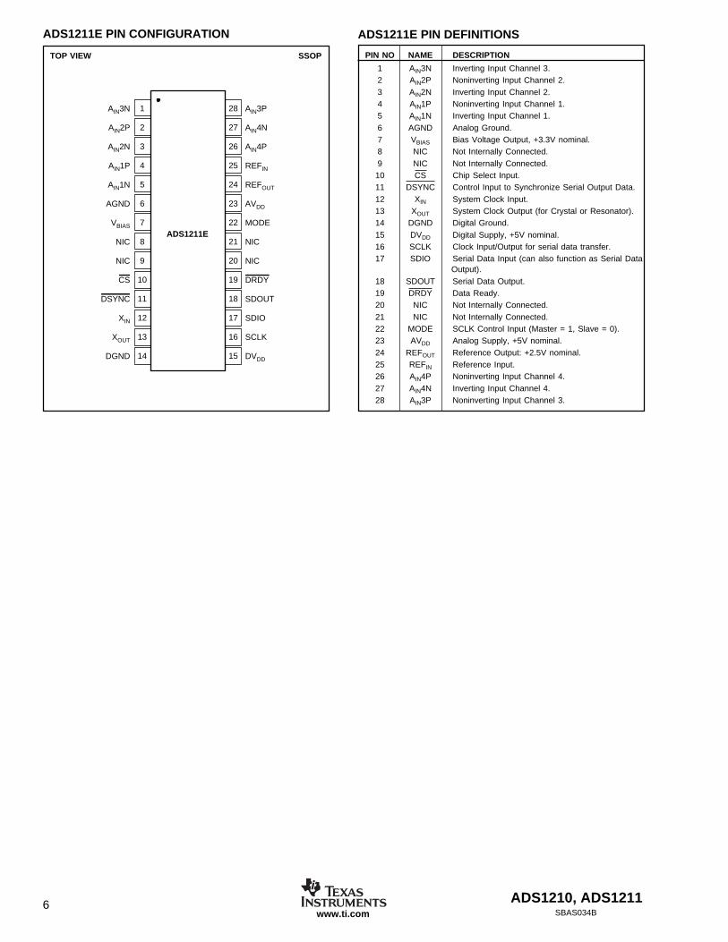
ADS1211E PIN DEFINITIONS
PIN NO NAME DESCRIPTION
1 AIN3N Inverting Input Channel 3.2 AIN2P Noninverting Input Channel 2.3 AIN2N Inverting Input Channel 2.4 AIN1P Noninverting Input Channel 1.5 AIN1N Inverting Input Channel 1.6 AGND Analog Ground.7 VBIAS Bias Voltage Output, +3.3V nominal.8 NIC Not Internally Connected.9 NIC Not Internally Connected.10 CS Chip Select Input.11 DSYNC Control Input to Synchronize Serial Output Data.12 XIN System Clock Input.13 XOUT System Clock Output (for Crystal or Resonator).14 DGND Digital Ground.15 DVDD Digital Supply, +5V nominal.16 SCLK Clock Input/Output for serial data transfer.17 SDIO Serial Data Input (can also function as Serial Data
Output).18 SDOUT Serial Data Output.19 DRDY Data Ready.20 NIC Not Internally Connected.21 NIC Not Internally Connected.22 MODE SCLK Control Input (Master = 1, Slave = 0).23 AVDD Analog Supply, +5V nominal.24 REFOUT Reference Output: +2.5V nominal.25 REFIN Reference Input.26 AIN4P Noninverting Input Channel 4.27 AIN4N Inverting Input Channel 4.28 AIN3P Noninverting Input Channel 3.
ADS1211E PIN CONFIGURATION
TOP VIEW SSOP
ADS1210, ADS1211 7SBAS034B www.ti.com
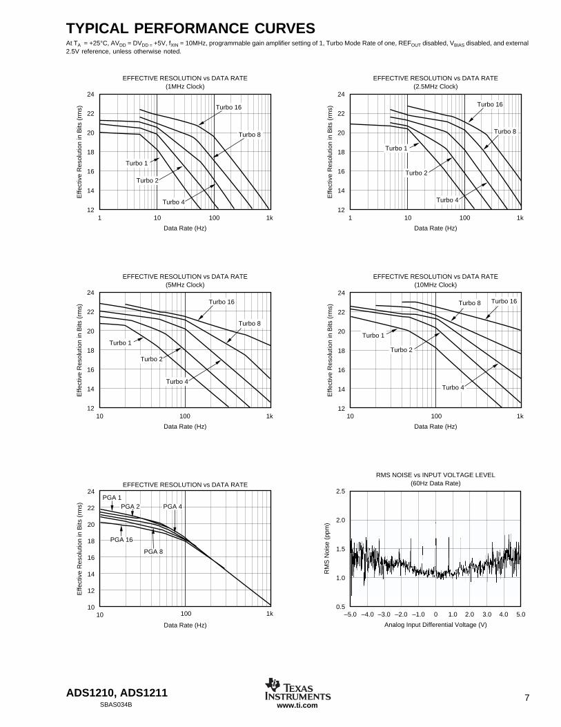
TYPICAL PERFORMANCE CURVESAt TA = +25°C, AVDD = DVDD = +5V, fXIN = 10MHz, programmable gain amplifier setting of 1, Turbo Mode Rate of one, REFOUT disabled, VBIAS disabled, and external2.5V reference, unless otherwise noted.
RMS NOISE vs INPUT VOLTAGE LEVEL(60Hz Data Rate)
Analog Input Differential Voltage (V)
–5.0 –4.0 –3.0 –2.0 –1.0 0 1.0 2.0 3.0 4.0 5.0
RM
S N
oise
(pp
m)
2.5
2.0
1.5
1.0
0.5
24
22
20
18
16
14
12
EFFECTIVE RESOLUTION vs DATA RATE(2.5MHz Clock)
Data Rate (Hz)
1 10 100 1k
Effe
ctiv
e R
esol
utio
n in
Bits
(rm
s)
Turbo 1
Turbo 2
Turbo 4
Turbo 8
Turbo 16
24
22
20
18
16
14
12
EFFECTIVE RESOLUTION vs DATA RATE(5MHz Clock)
Data Rate (Hz)
10 100 1k
Effe
ctiv
e R
esol
utio
n in
Bits
(rm
s)
Turbo 1
Turbo 2
Turbo 4
Turbo 8
Turbo 16
EFFECTIVE RESOLUTION vs DATA RATE(10MHz Clock)
Data Rate (Hz)
10 100 1k
Effe
ctiv
e R
esol
utio
n in
Bits
(rm
s)Turbo 1
Turbo 2
Turbo 4
Turbo 8 Turbo 1624
22
20
18
16
14
12
EFFECTIVE RESOLUTION vs DATA RATE
Data Rate (Hz)
10 100 1k
Effe
ctiv
e R
esol
utio
n in
Bits
(rm
s)
PGA 124
22
20
18
16
14
12
10
PGA 2 PGA 4
PGA 16
PGA 8
24
22
20
18
16
14
12
EFFECTIVE RESOLUTION vs DATA RATE(1MHz Clock)
Data Rate (Hz)
1 10 100 1k
Effe
ctiv
e R
esol
utio
n in
Bits
(rm
s)
Turbo 1
Turbo 2
Turbo 4
Turbo 8
Turbo 16
ADS1210, ADS12118SBAS034Bwww.ti.com
POWER DISSIPATION vs TURBO MODE RATE(REFOUT Enabled)
Turbo Mode Rate
10MHz
1 2 4 8 16
Pow
er D
issi
patio
n (m
W)
50.0
40.0
30.0
20.0
5MHz
2.5MHz
1MHz
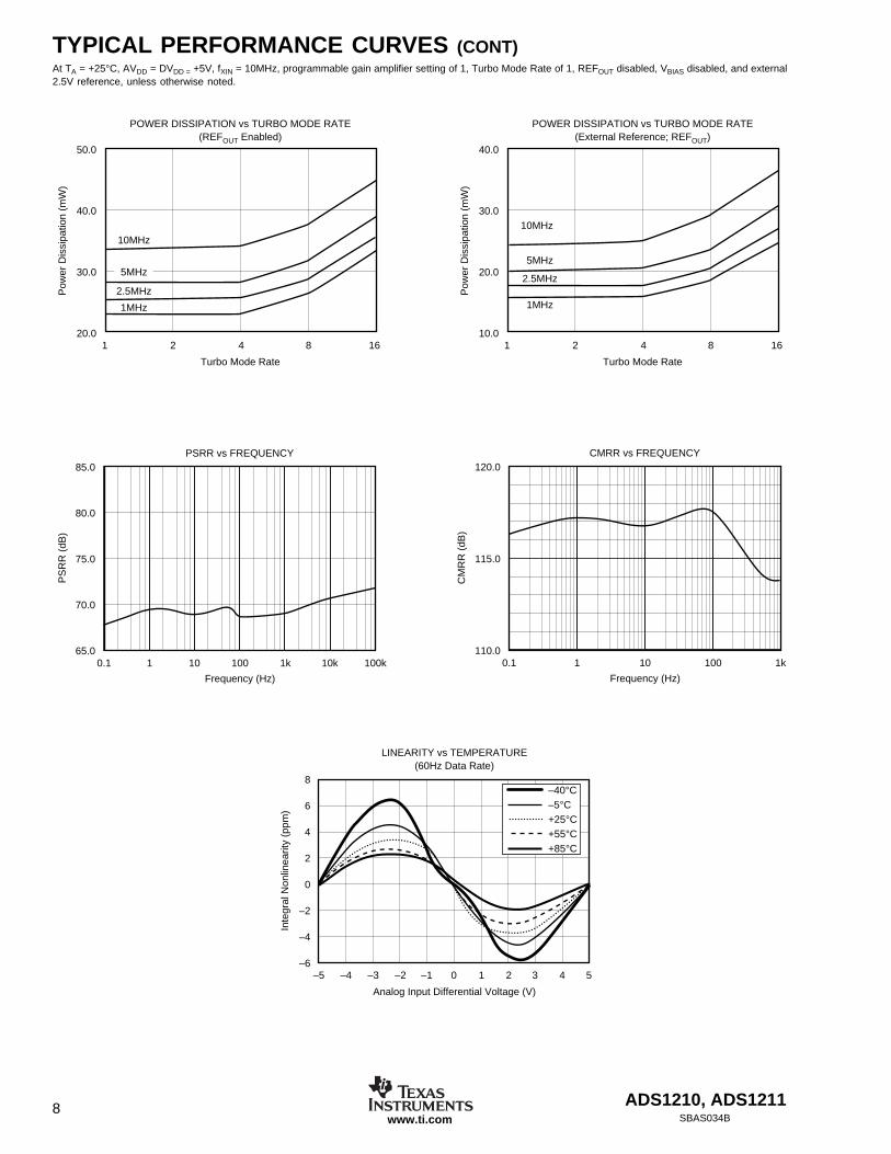
TYPICAL PERFORMANCE CURVES (CONT)At TA = +25°C, AVDD = DVDD = +5V, fXIN = 10MHz, programmable gain amplifier setting of 1, Turbo Mode Rate of 1, REFOUT disabled, VBIAS disabled, and external2.5V reference, unless otherwise noted.
85.0
80.0
75.0
70.0
65.0
PSRR vs FREQUENCY
PS
RR
(dB
)
0.1 1 10 100
Frequency (Hz)
1k 10k 100k
120.0
115.0
110.0
CMRR vs FREQUENCYC
MR
R (
dB)
0.1 1 10
Frequency (Hz)
100 1k
POWER DISSIPATION vs TURBO MODE RATE(External Reference; REFOUT)
Turbo Mode Rate
10MHz
1 2 4 8 16
Pow
er D
issi
patio
n (m
W)
40.0
30.0
20.0
10.0
5MHz
2.5MHz
1MHz
LINEARITY vs TEMPERATURE(60Hz Data Rate)
Analog Input Differential Voltage (V)
–5 –4 –3 –2 –1 0 1 2 3 4 5
Inte
gral
Non
linea
rity
(ppm
)
8
6
4
2
0
–2
–4
–6
–40°C–5°C+25°C+55°C+85°C
ADS1210, ADS1211 9SBAS034B www.ti.com
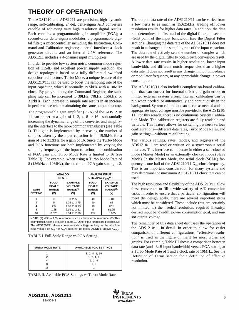
ANALOG ANALOG INPUTINPUT(1) UTILIZING VBIAS
(1,2)
FULL- EXAMPLE FULL- EXAMPLESCALE VOLTAGE SCALE VOLTAGE
GAIN RANGE RANGE(3) RANGE RANGE(3)
SETTING (V) (V) (V) (V)
1 10 0 to 5 40 ±102 5 1.25 to 3.75 20 ±54 2.5 1.88 to 3.13 10 ±2.58 1.25 2.19 to 2.81 5 ±1.25
16 0.625 2.34 to 2.66 2.5 ±0.625
NOTE: (1) With a 2.5V reference, such as the internal reference. (2) Thisexample utilizes the circuit in Figure 12. Other input ranges are possible. (3)The ADS1210/11 allows common-mode voltage as long as the absoluteinput voltage on AINP or AINN does not go below AGND or above AVDD.
THEORY OF OPERATIONThe ADS1210 and ADS1211 are precision, high dynamicrange, self-calibrating, 24-bit, delta-sigma A/D converterscapable of achieving very high resolution digital results.Each contains a programmable gain amplifier (PGA); asecond-order delta-sigma modulator; a programmable digi-tal filter; a microcontroller including the Instruction, Com-mand and Calibration registers; a serial interface; a clockgenerator circuit; and an internal 2.5V reference. TheADS1211 includes a 4-channel input multiplexer.
In order to provide low system noise, common-mode rejec-tion of 115dB and excellent power supply rejection, thedesign topology is based on a fully differential switchedcapacitor architecture. Turbo Mode, a unique feature of theADS1210/11, can be used to boost the sampling rate of theinput capacitor, which is normally 19.5kHz with a 10MHzclock. By programming the Command Register, the sam-pling rate can be increased to 39kHz, 78kHz, 156kHz, or312kHz. Each increase in sample rate results in an increasein performance when maintaining the same output data rate.
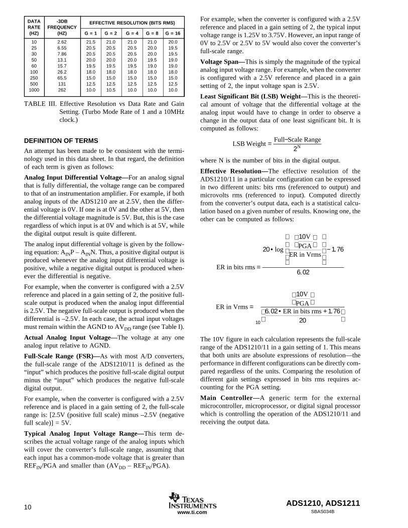
The programmable gain amplifier (PGA) of the ADS1210/11 can be set to a gain of 1, 2, 4, 8 or 16—substantiallyincreasing the dynamic range of the converter and simplify-ing the interface to the more common transducers (see TableI). This gain is implemented by increasing the number ofsamples taken by the input capacitor from 19.5kHz for again of 1 to 312kHz for a gain of 16. Since the Turbo Modeand PGA functions are both implemented by varying thesampling frequency of the input capacitor, the combinationof PGA gain and Turbo Mode Rate is limited to 16 (seeTable II). For example, when using a Turbo Mode Rate of8 (156kHz at 10MHz), the maximum PGA gain setting is 2.
TABLE I. Full-Scale Range vs PGA Setting.
TURBO MODE RATE AVAILABLE PGA SETTINGS
1 1, 2, 4, 8, 162 1, 2, 4, 84 1, 2, 48 1, 2
16 1
TABLE II. Available PGA Settings vs Turbo Mode Rate.
The output data rate of the ADS1210/11 can be varied froma few hertz to as much as 15,625kHz, trading off lowerresolution results for higher data rates. In addition, the datarate determines the first null of the digital filter and sets the–3dB point of the input bandwidth (see the Digital Filtersection). Changing the data rate of the ADS1210/11 does notresult in a change in the sampling rate of the input capacitor.The data rate effectively sets the number of samples whichare used by the digital filter to obtain each conversion result.A lower data rate results in higher resolution, lower inputbandwidth, and different notch frequencies than a higherdata rate. It does not result in any change in input impedanceor modulator frequency, or any appreciable change in powerconsumption.
The ADS1210/11 also includes complete on-board calibra-tion that can correct for internal offset and gain errors orlimited external system errors. Internal calibration can berun when needed, or automatically and continuously in thebackground. System calibration can be run as needed and theappropriate input voltages must be provided to the ADS1210/11. For this reason, there is no continuous System Calibra-tion Mode. The calibration registers are fully readable andwritable. This feature allows for switching between variousconfigurations—different data rates, Turbo Mode Rates, andgain settings—without re-calibrating.
The various settings, rates, modes, and registers of theADS1210/11 are read or written via a synchronous serialinterface. This interface can operate in either a self-clockedmode (Master Mode) or an externally clocked mode (SlaveMode). In the Master Mode, the serial clock (SCLK) fre-quency is one-half of the ADS1210/11 XIN clock frequency.This is an important consideration for many systems andmay determine the maximum ADS1210/11 clock that can beused.
The high resolution and flexibility of the ADS1210/11 allowthese converters to fill a wide variety of A/D conversiontasks. In order to ensure that a particular configuration willmeet the design goals, there are several important itemswhich must be considered. These include (but are certainlynot limited to) the needed resolution, required linearity,desired input bandwidth, power consumption goal, and sen-sor output voltage.
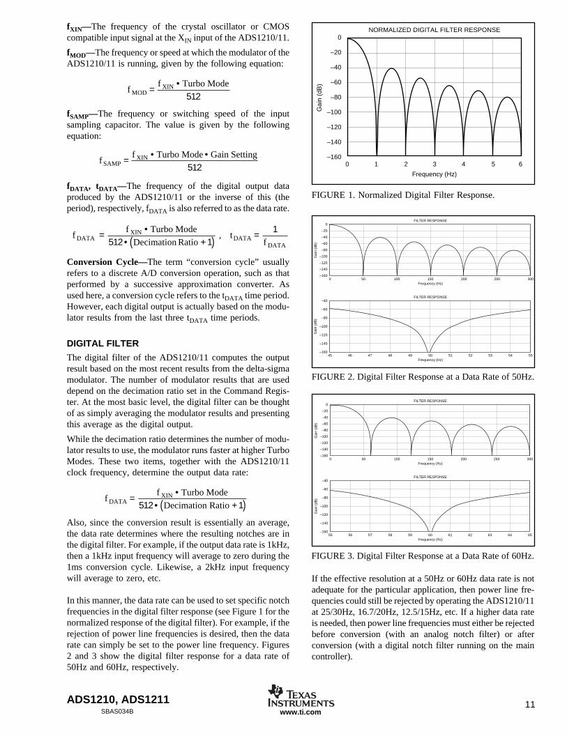
The remainder of this data sheet discusses the operation ofthe ADS1210/11 in detail. In order to allow for easiercomparison of different configurations, “effective resolu-tion” is used as the figure of merit for most tables andgraphs. For example, Table III shows a comparison betweendata rate (and –3dB input bandwidth) versus PGA setting ata Turbo Mode Rate of 1 and a clock rate of 10MHz. See theDefinition of Terms section for a definition of effectiveresolution.
ADS1210, ADS121110SBAS034Bwww.ti.com
DATA -3DBRATE FREQUENCY(HZ) (HZ) G = 1 G = 2 G = 4 G = 8 G = 16
10 2.62 21.5 21.0 21.0 21.0 20.025 6.55 20.5 20.5 20.5 20.0 19.530 7.86 20.5 20.5 20.5 20.0 19.550 13.1 20.0 20.0 20.0 19.5 19.060 15.7 19.5 19.5 19.5 19.0 19.0
100 26.2 18.0 18.0 18.0 18.0 18.0250 65.5 15.0 15.0 15.0 15.0 15.0500 131 12.5 12.5 12.5 12.5 12.51000 262 10.0 10.5 10.0 10.0 10.0
EFFECTIVE RESOLUTION (BITS RMS)
TABLE III. Effective Resolution vs Data Rate and GainSetting. (Turbo Mode Rate of 1 and a 10MHzclock.)
DEFINITION OF TERMS
An attempt has been made to be consistent with the termi-nology used in this data sheet. In that regard, the definitionof each term is given as follows:
Analog Input Differential Voltage—For an analog signalthat is fully differential, the voltage range can be comparedto that of an instrumentation amplifier. For example, if bothanalog inputs of the ADS1210 are at 2.5V, then the differ-ential voltage is 0V. If one is at 0V and the other at 5V, thenthe differential voltage magnitude is 5V. But, this is the caseregardless of which input is at 0V and which is at 5V, whilethe digital output result is quite different.
The analog input differential voltage is given by the follow-ing equation: AINP – AINN. Thus, a positive digital output isproduced whenever the analog input differential voltage ispositive, while a negative digital output is produced when-ever the differential is negative.
For example, when the converter is configured with a 2.5Vreference and placed in a gain setting of 2, the positive full-scale output is produced when the analog input differentialis 2.5V. The negative full-scale output is produced when thedifferential is –2.5V. In each case, the actual input voltagesmust remain within the AGND to AVDD range (see Table I).
Actual Analog Input Voltage—The voltage at any oneanalog input relative to AGND.
Full-Scale Range (FSR)—As with most A/D converters,the full-scale range of the ADS1210/11 is defined as the“input” which produces the positive full-scale digital outputminus the “input” which produces the negative full-scaledigital output.
For example, when the converter is configured with a 2.5Vreference and is placed in a gain setting of 2, the full-scalerange is: [2.5V (positive full scale) minus –2.5V (negativefull scale)] = 5V.
Typical Analog Input Voltage Range—This term de-scribes the actual voltage range of the analog inputs whichwill cover the converter’s full-scale range, assuming thateach input has a common-mode voltage that is greater thanREFIN/PGA and smaller than (AVDD – REFIN/PGA).
LSB Weight = Full−Scale Range
2N
For example, when the converter is configured with a 2.5Vreference and placed in a gain setting of 2, the typical inputvoltage range is 1.25V to 3.75V. However, an input range of0V to 2.5V or 2.5V to 5V would also cover the converter’sfull-scale range.
Voltage Span—This is simply the magnitude of the typicalanalog input voltage range. For example, when the converteris configured with a 2.5V reference and placed in a gainsetting of 2, the input voltage span is 2.5V.
Least Significant Bit (LSB) Weight—This is the theoreti-cal amount of voltage that the differential voltage at theanalog input would have to change in order to observe achange in the output data of one least significant bit. It iscomputed as follows:
where N is the number of bits in the digital output.
Effective Resolution—The effective resolution of theADS1210/11 in a particular configuration can be expressedin two different units: bits rms (referenced to output) andmicrovolts rms (referenced to input). Computed directlyfrom the converter’s output data, each is a statistical calcu-lation based on a given number of results. Knowing one, theother can be computed as follows:
The 10V figure in each calculation represents the full-scalerange of the ADS1210/11 in a gain setting of 1. This meansthat both units are absolute expressions of resolution—theperformance in different configurations can be directly com-pared regardless of the units. Comparing the resolution ofdifferent gain settings expressed in bits rms requires ac-counting for the PGA setting.
Main Controller—A generic term for the externalmicrocontroller, microprocessor, or digital signal processorwhich is controlling the operation of the ADS1210/11 andreceiving the output data.
ER in bits rms =
20 • log
10VPGA
ER in Vrms
− 1.76
6.02
ER in Vrms =
10
10VPGA
6.02 • ER in bits rms + 1.7620
ADS1210, ADS1211 11SBAS034B www.ti.com
f DATA = f XIN • Turbo Mode
512 • Decimation Ratio + 1( )
f DATA = f XIN • Turbo Mode
512 • Decimation Ratio + 1( ) , tDATA = 1f DATA
FILTER RESPONSE
Frequency (Hz)
–40
–60
–80
–100
–120
–140
–16045 46 47 48 49 50 51 52 53 54 55
FILTER RESPONSE
Frequency (Hz)
0
–20
–40
–60
–80
–100
–120
–140
–1600 50 100 150 200 250 300
Gai
n (d
B)
Gai
n (d
B)
NORMALIZED DIGITAL FILTER RESPONSE
Frequency (Hz)
0
–20
–40
–60
–80
–100
–120
–140
–1600 1 2 3 4 5 6
Gai
n (d
B)
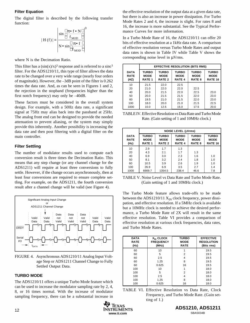
FIGURE 3. Digital Filter Response at a Data Rate of 60Hz.
f MOD = f XIN • Turbo Mode
512
f SAMP = f XIN • Turbo Mode • Gain Setting
512
FIGURE 1. Normalized Digital Filter Response.
FIGURE 2. Digital Filter Response at a Data Rate of 50Hz.
If the effective resolution at a 50Hz or 60Hz data rate is notadequate for the particular application, then power line fre-quencies could still be rejected by operating the ADS1210/11at 25/30Hz, 16.7/20Hz, 12.5/15Hz, etc. If a higher data rateis needed, then power line frequencies must either be rejectedbefore conversion (with an analog notch filter) or afterconversion (with a digital notch filter running on the maincontroller).
fXIN—The frequency of the crystal oscillator or CMOScompatible input signal at the XIN input of the ADS1210/11.
fMOD—The frequency or speed at which the modulator of theADS1210/11 is running, given by the following equation:
fSAMP—The frequency or switching speed of the inputsampling capacitor. The value is given by the followingequation:
fDATA, tDATA—The frequency of the digital output dataproduced by the ADS1210/11 or the inverse of this (theperiod), respectively, fDATA is also referred to as the data rate.
Conversion Cycle—The term “conversion cycle” usuallyrefers to a discrete A/D conversion operation, such as thatperformed by a successive approximation converter. Asused here, a conversion cycle refers to the tDATA time period.However, each digital output is actually based on the modu-lator results from the last three tDATA time periods.
DIGITAL FILTER
The digital filter of the ADS1210/11 computes the outputresult based on the most recent results from the delta-sigmamodulator. The number of modulator results that are useddepend on the decimation ratio set in the Command Regis-ter. At the most basic level, the digital filter can be thoughtof as simply averaging the modulator results and presentingthis average as the digital output.
While the decimation ratio determines the number of modu-lator results to use, the modulator runs faster at higher TurboModes. These two items, together with the ADS1210/11clock frequency, determine the output data rate:
Also, since the conversion result is essentially an average,the data rate determines where the resulting notches are inthe digital filter. For example, if the output data rate is 1kHz,then a 1kHz input frequency will average to zero during the1ms conversion cycle. Likewise, a 2kHz input frequencywill average to zero, etc.
In this manner, the data rate can be used to set specific notchfrequencies in the digital filter response (see Figure 1 for thenormalized response of the digital filter). For example, if therejection of power line frequencies is desired, then the datarate can simply be set to the power line frequency. Figures2 and 3 show the digital filter response for a data rate of50Hz and 60Hz, respectively.
FILTER RESPONSE
Frequency (Hz)
–40
–60
–80
–100
–120
–140
–16055 56 57 58 59 60 61 62 63 64 65
FILTER RESPONSE
Frequency (Hz)
0
–20
–40
–60
–80
–100
–120
–140
–1600 50 100 150 200 250 300
Gai
n (d
B)
Gai
n (d
B)
ADS1210, ADS121112SBAS034Bwww.ti.com
Filter Equation
The digital filter is described by the following transferfunction:
where N is the Decimation Ratio.
This filter has a (sin(x)/x)3 response and is referred to a sinc3
filter. For the ADS1210/11, this type of filter allows the datarate to be changed over a very wide range (nearly four ordersof magnitude). However, the –3dB point of the filter is 0.262times the data rate. And, as can be seen in Figures 1 and 2,the rejection in the stopband (frequencies higher than thefirst notch frequency) may only be –40dB.
These factors must be considered in the overall systemdesign. For example, with a 50Hz data rate, a significantsignal at 75Hz may alias back into the passband at 25Hz.The analog front end can be designed to provide the neededattenuation to prevent aliasing, or the system may simplyprovide this inherently. Another possibility is increasing thedata rate and then post filtering with a digital filter on themain controller.
Filter Settling
The number of modulator results used to compute eachconversion result is three times the Decimation Ratio. Thismeans that any step change (or any channel change for theADS1211) will require at least three conversions to fullysettle. However, if the change occurs asynchronously, then atleast four conversions are required to ensure complete set-tling. For example, on the ADS1211, the fourth conversionresult after a channel change will be valid (see Figure 4).
| H (f ) | =sin
π • f • Nf MOD
N • sinπ • ff MOD
3
the effective resolution of the output data at a given data rate,but there is also an increase in power dissipation. For TurboMode Rates 2 and 4, the increase is slight. For rates 8 and16, the increase is more substantial. See the Typical Perfor-mance Curves for more information.
In a Turbo Mode Rate of 16, the ADS1210/11 can offer 20bits of effective resolution at a 1kHz data rate. A comparisonof effective resolution versus Turbo Mode Rates and outputdata rates is shown in Table IV while Table V shows thecorresponding noise level in µVrms.
TURBO MODE
The ADS1210/11 offers a unique Turbo Mode feature whichcan be used to increase the modulator sampling rate by 2, 4,8, or 16 times normal. With the increase of modulatorsampling frequency, there can be a substantial increase in
DATA TURBO TURBO TURBO TURBO TURBORATE MODE MODE MODE MODE MODE(HZ) RATE 1 RATE 2 RATE 4 RATE 8 RATE 16
10 21.5 22.0 22.520 21.0 22.0 22.0 22.540 20.0 21.5 22.0 22.5 23.050 20.0 21.5 21.5 22.0 23.060 19.5 21.0 21.5 22.0 23.0100 18.0 20.0 21.0 21.5 22.51000 10.0 12.5 15.0 17.5 20.0
EFFECTIVE RESOLUTION (BITS RMS)
TABLE IV. Effective Resolution vs Data Rate and Turbo ModeRate. (Gain setting of 1 and 10MHz clock.)
DATA TURBO TURBO TURBO TURBO TURBORATE MODE MODE MODE MODE MODE(Hz) RATE 1 RATE 2 RATE 4 RATE 8 RATE 16
10 2.9 1.7 1.320 4.3 2.1 1.7 1.340 6.9 3.0 2.3 1.6 1.050 8.1 3.2 2.4 1.8 1.060 10.5 3.9 2.6 1.9 1.0100 26.9 6.9 3.5 2.7 1.41000 6909.7 1354.5 238.4 46.6 7.8
TABLE V. Noise Level vs Data Rate and Turbo Mode Rate.(Gain setting of 1 and 10MHz clock.)
NOISE LEVEL (µVrms)
The Turbo Mode feature allows trade-offs to be madebetween the ADS1210/11 XIN clock frequency, power dissi-pation, and effective resolution. If a 5MHz clock is availablebut a 10MHz clock is needed to achieve the desired perfor-mance, a Turbo Mode Rate of 2X will result in the sameeffective resolution. Table VI provides a comparison ofeffective resolution at various clock frequencies, data rates,and Turbo Mode Rates.
DATA XIN CLOCK TURBO EFFECTIVERATE FREQUENCY MODE RESOLUTION(Hz) (MHz) RATE (Bits rms)
60 10 1 19.560 5 2 19.560 2.5 4 19.560 1.25 8 19.560 0.625 16 19.5100 10 1 18.0100 5 2 18.0100 2.5 4 18.0100 1.25 8 18.0100 0.625 16 18.0
TABLE VI. Effective Resolution vs Data Rate, ClockFrequency, and Turbo Mode Rate. (Gain set-ting of 1.)
FIGURE 4. Asynchronous ADS1210/11 Analog Input Volt-age Step or ADS1211 Channel Change to FullySettled Output Data.
DRDY
SerialI/O
ValidData
ValidData
ValidData
ValidData
Datanot
Valid
Datanot
Valid
Datanot
Valid
Significant Analog Input Changeor
ADS1211 Channel Change
tDATA
ADS1210, ADS1211 13SBAS034B www.ti.com
The Turbo Mode Rate (TMR) is programmed via the Sam-pling Frequency bits of the Command Register. Due to theincrease in input capacitor sampling frequency, higher TurboMode settings result in lower analog input impedance;
AIN Impedance (Ω) = (10MHz/fXIN)•4.3E6/(G•TMR)
where G is the gain setting. Because the modulator rate alsochanges in direct relation to the Turbo Mode setting, highervalues result in a lower impedance for the REFIN input:
REFIN Impedance (Ω) = (10MHz/fXIN)•1E6/TMR
The Turbo Mode Rate can be set to 1, 2, 4, 8, or 16. Consultthe graphs shown in the Typical Performance Curves for fulldetails on the performance of the ADS1210/11 operating indifferent Turbo Mode Rates. Keep in mind that higher TurboMode Rates result in fewer available gain settings as shownin Table II.
PROGRAMMABLE GAIN AMPLIFIER
The programmable gain amplifier gain setting is programmedvia the PGA Gain bits of the Command Register. Changesin the gain setting (G) of the programmable gain amplifierresults in an increase in the input capacitor sampling fre-quency. Thus, higher gain settings result in a lower analoginput impedance:
AIN Impedance (Ω) = (10MHz/fXIN)•4.3E6/(G•TMR)
where TMR is the Turbo Mode Rate. Because the modulatorspeed does not depend on the gain setting, the input imped-ance seen at REFIN does not change.
The PGA can be set to gains of 1, 2, 4, 8, or 16. These gainsettings with their resulting full-scale range and typicalvoltage range are shown in Table I. Keep in mind that higherTurbo Mode Rates result in fewer available gain settings asshown in Table II.
SOFTWARE GAIN
The excellent performance, flexibility, and low cost of theADS1210/11 allow the converter to be considered for de-signs which would not normally need a 24-bit ADC. Forexample, many designs utilize a 12-bit converter and a high-gain INA or PGA for digitizing low amplitude signals. Forsome of these cases, the ADS1210/11 by itself may be asolution, even though the maximum gain is limited to 16.
To get around the gain limitation, the digital result cansimply be shifted up by “n” bits in the main controller—resulting in a gain of “n” times G, where G is the gainsetting. While this type of manipulation of the output datais obvious, it is easy to miss how much the gain can beincreased in this manner on a 24-bit converter.
For example, shifting the result up by three bits when theADS1210/11 is set to a gain of 16 results in an effective gainof 128. At lower data rates, the converter can easily providemore than 12 bits of resolution. Even higher gains arepossible. The limitation is a combination of the needed datarate, desired noise performance, and desired linearity.
CALIBRATION
The ADS1210/11 offers several different types of calibra-tion, and the particular calibration desired is programmedvia the Command Register. In the case of BackgroundCalibration, the calibration will repeat at regular intervalsindefinitely. For all others, the calibration is performed onceand then normal operation is resumed.
Each type of calibration is covered in detail in its respectivesection. In general, calibration is recommended immediatelyafter power-on and whenever there is a “significant” changein the operating environment. The amount of change whichshould cause a re-calibration is dependent on the applica-tion, effective resolution, etc. Where high accuracy is impor-tant, re-calibration should be done on changes in tempera-ture and power supply. In all cases, re-calibration should bedone when the gain, Turbo Mode, or data rate is changed.
After a calibration has been accomplished, the Offset Cali-bration Register and the Full-Scale Calibration Registercontain the results of the calibration. The data in theseregisters are accurate to the effective resolution of theADS1210/11’s mode of operation during the calibration.Thus, these values will show a variation (or noise) equiva-lent to a regular conversion result.
For those cases where this error must be reduced, it istempting to consider running the calibration at a slower datarate and then increasing the converter’s data rate after thecalibration is complete. Unfortunately, this will not work asexpected. The reason is that the results calculated at theslower data rate would not be valid for the higher data rate.Instead, the calibration should be done repeatedly. Aftereach calibration, the results can be read and stored. After thedesired number of calibrations, the main controller cancompute an average and write this value into the calibrationregisters. The resulting error in the calibration values will bereduced by the square root of the number of calibrationswhich were averaged.
The calibration registers can also be used to provide systemoffset and gain corrections separate from those computed bythe ADS1210/11. For example, these might be burned intoE2PROM during final product testing. On power-on, themain controller would load these values into the calibrationregisters. A further possibility is a look-up table based on thecurrent temperature.
Note that the values in the calibration registers will vary fromconfiguration to configuration and from part to part. There isno method of reliably computing what a particular calibrationregister should be to correct for a given amount of systemerror. It is possible to present the ADS1210/11 with a knownamount of error, perform a calibration, read the desiredcalibration register, change the error value, perform anothercalibration, read the new value and use these values tointerpolate an intermediate value.
ADS1210, ADS121114SBAS034Bwww.ti.com
ValidData
DRDY
SerialI/O
ValidData
SOC(1)
tDATA
NormalMode
OffsetCalibration on
System Offset(2)
AnalogInput
Conversion
System OffsetCalibration Mode
PossiblyValidData
PossiblyValidData
NormalMode
NOTES: (1) SOC = System Offset Calibration instruction.(2) In Slave Mode, this function requires 4 cycles.
ValidData
DRDY
SerialI/O
ValidData
SC(1)
tDATA
NormalMode
ValidData
ValidData
NormalMode
OffsetCalibration on
Internal Offset(2)
Self-CalibrationMode
Full-ScaleCalibration on
Internal Full-Scale
AnalogInput
Conversion
NOTES: (1) SC = Self-Calibration instruction. (2) In Slave Mode, this function requires 4 cycles.
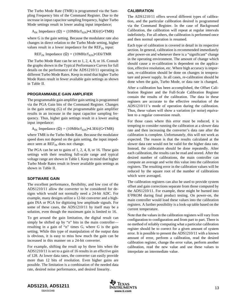
FIGURE 5. Self-Calibration Timing.
Mode bits are reset to 000 (Normal Mode). A single conver-sion is done with DRDY HIGH. After this conversion, theDRDY signal goes LOW indicating resumption of normaloperation.
Normal operation returns within a single conversion cyclebecause it is assumed that the input voltage at the converter’sinput is not removed immediately after the offset calibrationis performed. In this case, the digital filter already containsa valid result.
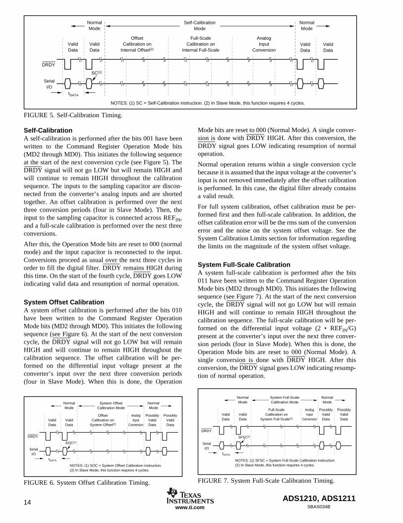
For full system calibration, offset calibration must be per-formed first and then full-scale calibration. In addition, theoffset calibration error will be the rms sum of the conversionerror and the noise on the system offset voltage. See theSystem Calibration Limits section for information regardingthe limits on the magnitude of the system offset voltage.
System Full-Scale CalibrationA system full-scale calibration is performed after the bits011 have been written to the Command Register OperationMode bits (MD2 through MD0). This initiates the followingsequence (see Figure 7). At the start of the next conversioncycle, the DRDY signal will not go LOW but will remainHIGH and will continue to remain HIGH throughout thecalibration sequence. The full-scale calibration will be per-formed on the differential input voltage (2 • REFIN/G)present at the converter’s input over the next three conver-sion periods (four in Slave Mode). When this is done, theOperation Mode bits are reset to 000 (Normal Mode). Asingle conversion is done with DRDY HIGH. After thisconversion, the DRDY signal goes LOW indicating resump-tion of normal operation.
FIGURE 7. System Full-Scale Calibration Timing.
Self-CalibrationA self-calibration is performed after the bits 001 have beenwritten to the Command Register Operation Mode bits(MD2 through MD0). This initiates the following sequenceat the start of the next conversion cycle (see Figure 5). TheDRDY signal will not go LOW but will remain HIGH andwill continue to remain HIGH throughout the calibrationsequence. The inputs to the sampling capacitor are discon-nected from the converter’s analog inputs and are shortedtogether. An offset calibration is performed over the nextthree conversion periods (four in Slave Mode). Then, theinput to the sampling capacitor is connected across REFIN,and a full-scale calibration is performed over the next threeconversions.
After this, the Operation Mode bits are reset to 000 (normalmode) and the input capacitor is reconnected to the input.Conversions proceed as usual over the next three cycles inorder to fill the digital filter. DRDY remains HIGH duringthis time. On the start of the fourth cycle, DRDY goes LOWindicating valid data and resumption of normal operation.
System Offset CalibrationA system offset calibration is performed after the bits 010have been written to the Command Register OperationMode bits (MD2 through MD0). This initiates the followingsequence (see Figure 6). At the start of the next conversioncycle, the DRDY signal will not go LOW but will remainHIGH and will continue to remain HIGH throughout thecalibration sequence. The offset calibration will be per-formed on the differential input voltage present at theconverter’s input over the next three conversion periods(four in Slave Mode). When this is done, the Operation
FIGURE 6. System Offset Calibration Timing.
ValidData
DRDY
SerialI/O
ValidData
SFSC(1)
tDATA
NormalMode
Full-ScaleCalibration on
System Full-Scale(2)
AnalogInput
Conversion
System Full-ScaleCalibration Mode
PossiblyValidData
PossiblyValidData
NormalMode
NOTES: (1) SFSC = System Full-Scale Calibration instruction.(2) In Slave Mode, this function requires 4 cycles.
ADS1210, ADS1211 15SBAS034B www.ti.com
NormalMode
Background CalibrationMode
ValidData
DRDY
SerialI/O
ValidData
BC(1)
tDATA
OffsetCalibration on
Internal Offset(2)
AnalogInput
Conversion
AnalogInput
Conversion
Cycle Repeatswith OffsetCalibration
Full-ScaleCalibration on
Internal Full-Scale
NOTES: (1) BC = Background Calibration instruction. (2) In Slave Mode, the very first offsetcalibration will require 4 cycles. All subsequent offset calibrations will require 3 cycles.
Normal operation returns within a single conversion cyclebecause it is assumed that the input voltage at the converter’sinput is not removed immediately after the full-scale calibra-tion is performed. In this case, the digital filter alreadycontains a valid result.
For full system calibration, offset calibration must be per-formed first and then full-scale calibration. The calibrationerror will be a sum of the rms noise on the conversion resultand the input signal noise. See the System Calibration Limitssection for information regarding the limits on the magni-tude of the system full-scale voltage.
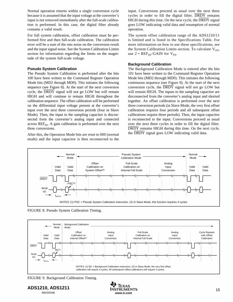
Pseudo System CalibrationThe Pseudo System Calibration is performed after the bits100 have been written to the Command Register OperationMode bits (MD2 through MD0). This initiates the followingsequence (see Figure 8). At the start of the next conversioncycle, the DRDY signal will not go LOW but will remainHIGH and will continue to remain HIGH throughout thecalibration sequence. The offset calibration will be performedon the differential input voltage present at the converter’sinput over the next three conversion periods (four in SlaveMode). Then, the input to the sampling capacitor is discon-nected from the converter’s analog input and connectedacross REFIN. A gain calibration is performed over the nextthree conversions.
After this, the Operation Mode bits are reset to 000 (normalmode) and the input capacitor is then reconnected to the
FIGURE 8. Pseudo System Calibration Timing.
FIGURE 9. Background Calibration Timing.
ValidData
DRDY
SerialI/O
ValidData
PSC(1)
tDATA
NormalMode
ValidData
ValidData
NormalMode
OffsetCalibration on
System Offset(2)
Pseudo SystemCalibration Mode
Full-ScaleCalibration on
Internal Full-Scale
AnalogInput
Conversion
NOTES: (1) PSC = Pseudo System Calibration instruction. (2) In Slave Mode, this function requires 4 cycles.
input. Conversions proceed as usual over the next threecycles in order to fill the digital filter. DRDY remainsHIGH during this time. On the next cycle, the DRDY signalgoes LOW indicating valid data and resumption of normaloperation.
The system offset calibration range of the ADS1210/11is limited and is listed in the Specifications Table. Formore information on how to use these specifications, seethe System Calibration Limits section. To calculate VOS,use 2 • REFIN /GAIN for VFS.
Background CalibrationThe Background Calibration Mode is entered after the bits101 have been written to the Command Register OperationMode bits (MD2 through MD0). This initiates the followingcontinuous sequence (see Figure 9). At the start of the nextconversion cycle, the DRDY signal will not go LOW butwill remain HIGH. The inputs to the sampling capacitor aredisconnected from the converter’s analog input and shortedtogether. An offset calibration is performed over the nextthree conversion periods (in Slave Mode, the very first offsetcalibration requires four periods and all subsequent offsetcalibrations require three periods). Then, the input capacitoris reconnected to the input. Conversions proceed as usualover the next three cycles in order to fill the digital filter.DRDY remains HIGH during this time. On the next cycle,the DRDY signal goes LOW indicating valid data.
ADS1210, ADS121116SBAS034Bwww.ti.com
Also, during this cycle, the sampling capacitor is discon-nected from the converter’s analog input and is connectedacross REFIN. A gain calibration is initiated and proceedsover the next three conversions. After this, the input capaci-tor is once again connected to the analog input. Conversionsproceed as usual over the next three cycles in order to fill thedigital filter. DRDY remains HIGH during this time. On thenext cycle, the DRDY signal goes LOW indicating validdata, the input to the sampling capacitor is shorted, and anoffset calibration is initiated. At this point, the BackgroundCalibration sequence repeats.
In essence, the Background Calibration Mode performscontinuous self-calibration where the offset and gain cali-brations are interleaved with regular conversions. Thus, thedata rate is reduced by a factor of 6. The advantage is thatthe converter is continuously adjusting to environmentalchanges such as ambient or component temperature (due toairflow variations).
The ADS1210/11 will remain in the Background Calibra-tion Mode indefinitely. To move to any other mode, theCommand Register Operation Mode bits (MD2 throughMD0) must be set to the appropriate values.
System Calibration Offset and Full-ScaleCalibration LimitsThe System Offset and Full-Scale Calibration range of theADS1210/11 is limited and is listed in the SpecificationsTable. The range is specified as:
(VFS – | VOS |) < 1.3 • (2 • REFIN)/GAIN(VFS – | VOS |) > 0.7 • (2 • REFIN)/GAIN
where VFS is the system full-scale voltage and | VOS | is theabsolute value of the system offset voltage. In the followingdiscussion, keep in mind that these voltages are differentialvoltages.
For example, with the internal reference (2.5V) and a gain oftwo, the previous equations become (after some manipulation):
VFS – 3.25 < VOS < VFS – 1.75
If VFS is perfect at 2.5V (positive full-scale), then VOS mustbe greater than –0.75V and less than 0.75V. Thus, when offsetcalibration is performed, the positive input can be no morethan 0.75V below or above the negative input. If this range isexceeded, the ADS1210/11 may not calibrate properly.
This calculation method works for all gains other than one.For a gain of one and the internal reference (2.5V), theequation becomes:
VFS – 6.5 < VOS < VFS – 3.5
With a 5V positive full-scale input, VOS must be greater than–1.5V and less than 1.5V. Since the offset represents acommon-mode voltage and the input voltage range in a gainof one is 0V to 5V, a common-mode voltage will cause theactual input voltage to possibly go below 0V or above 5V.The specifications also show that for the specifications to bevalid, the input voltage must not go below AGND by morethan 30mV or above AVDD by more than 30mV.
This will be an important consideration in many systemswhich use a 2.5V or greater reference, as the input range isconstrained by the expected power supply variations. Inaddition, the expected full-scale voltage will impact theallowable offset voltage (and vice-versa) as the combinationof the two must remain within the power supply and groundpotentials, regardless of the results obtained via the rangecalculation shown previously.
There are only two solutions to this constraint: either thesystem design must ensure that the full-scale and offsetvoltage variations will remain within the power supply andground potentials, or the part must be used in a gain of 2 orgreater.
SLEEP MODE
The Sleep Mode is entered after the bits 110 have beenwritten to the Command Register Operation Mode bits(MD2 through MD0). This mode is exited by entering a newmode into the MD2-MD0 bits.
The Sleep Mode causes the analog section and a good dealof the digital section to power down. For full analog powerdown, the VBIAS generator and the internal reference mustalso be powered down by setting the BIAS and REFO bitsin the Command Register accordingly. The power dissipa-tion shown in the Specifications Table is with the internalreference and the VBIAS generator disabled.
To initiate serial communication with the converter while itis in Sleep Mode, one of the following procedures must beused: If CS is being used, simply taking CS LOW willenable serial communication to proceed normally. If CS isnot being used (tied LOW) and the ADS1210/11 is in theMaster Mode, then a falling edge must be produced on theSDIO line. If SDIO is LOW, the SDIO line must be takenHIGH for 2 • tXIN periods (minimum) and then taken LOW.Alternatively, SDIO can be forced HIGH after putting theADS1210/11 to “sleep” and then taken LOW when theSleep Mode is to be exited. Finally, if CS is not being used(tied LOW) and the ADS1210/11 is in the Slave Mode, thensimply sending a normal Instruction Register command willre-establish communication.
Once serial communication is resumed, the Sleep Mode isexited by changing the MD2-MD0 bits to any other mode.When a new mode (other than Sleep) has been entered, theADS1210/11 will execute a very brief internal power-upsequence of the analog and digital circuitry. Once this hasbeen done, one normal conversion cycle is performed beforethe new mode is actually entered. At the end of this conversioncycle, the new mode takes effect and the converter willrespond accordingly. The DRDY signal will remain HIGHthrough the first conversion cycle. It will also remain HIGHthrough the second, even if the new mode is the Normal Mode.
If the VBIAS generator and/or the internal reference havebeen disabled, then they must be manually re-enabled via theappropriate bits in the Command Register. In addition, theinternal reference will have to charge the external bypasscapacitor(s) and possibly other circuitry. There may also be
ADS1210, ADS1211 17SBAS034B www.ti.com
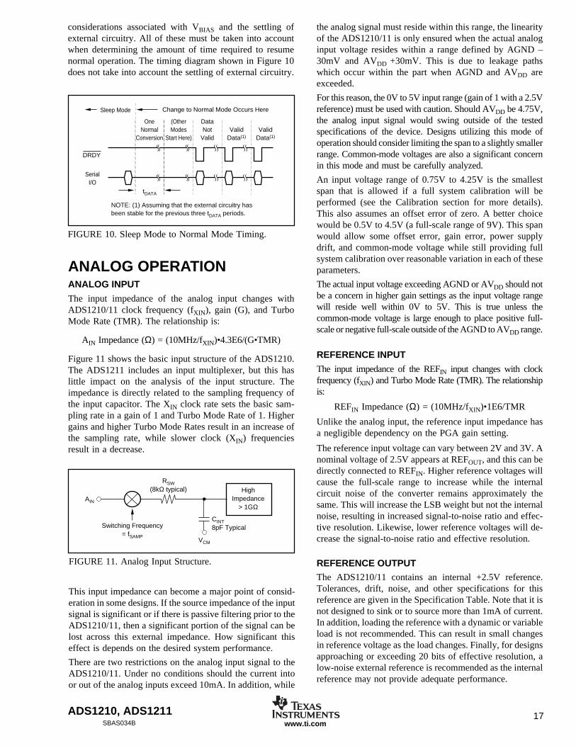
considerations associated with VBIAS and the settling ofexternal circuitry. All of these must be taken into accountwhen determining the amount of time required to resumenormal operation. The timing diagram shown in Figure 10does not take into account the settling of external circuitry.
FIGURE 10. Sleep Mode to Normal Mode Timing.
DRDY
SerialI/O
NOTE: (1) Assuming that the external circuitry hasbeen stable for the previous three tDATA periods.
tDATA
OneNormal
Conversion
(OtherModes
Start Here)
DataNot
ValidValid
Data(1)Valid
Data(1)
Sleep Mode Change to Normal Mode Occurs Here
ANALOG OPERATIONANALOG INPUT
The input impedance of the analog input changes withADS1210/11 clock frequency (fXIN), gain (G), and TurboMode Rate (TMR). The relationship is:
AIN Impedance (Ω) = (10MHz/fXIN)•4.3E6/(G•TMR)
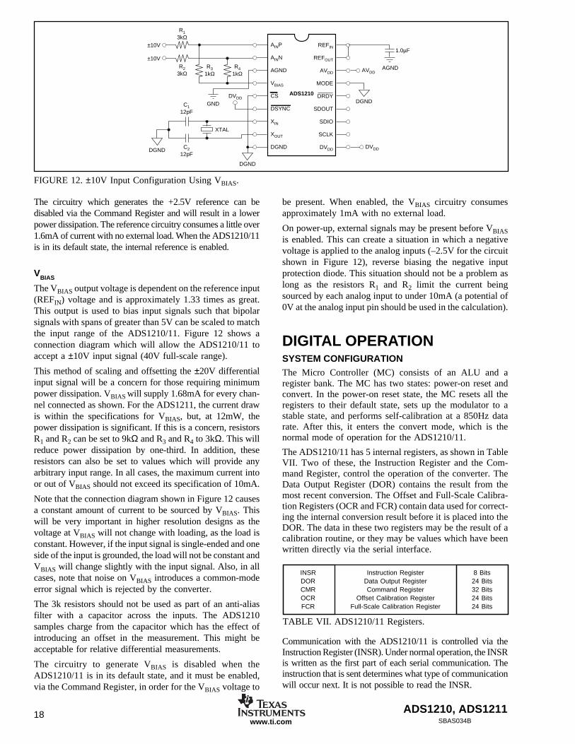
Figure 11 shows the basic input structure of the ADS1210.The ADS1211 includes an input multiplexer, but this haslittle impact on the analysis of the input structure. Theimpedance is directly related to the sampling frequency ofthe input capacitor. The XIN clock rate sets the basic sam-pling rate in a gain of 1 and Turbo Mode Rate of 1. Highergains and higher Turbo Mode Rates result in an increase ofthe sampling rate, while slower clock (XIN) frequenciesresult in a decrease.
FIGURE 11. Analog Input Structure.
RSW(8kΩ typical)
Switching Frequency= fSAMP
HighImpedance
> 1GΩ
CINT8pF Typical
VCM
AIN
This input impedance can become a major point of consid-eration in some designs. If the source impedance of the inputsignal is significant or if there is passive filtering prior to theADS1210/11, then a significant portion of the signal can belost across this external impedance. How significant thiseffect is depends on the desired system performance.
There are two restrictions on the analog input signal to theADS1210/11. Under no conditions should the current intoor out of the analog inputs exceed 10mA. In addition, while
the analog signal must reside within this range, the linearityof the ADS1210/11 is only ensured when the actual analoginput voltage resides within a range defined by AGND –30mV and AVDD +30mV. This is due to leakage pathswhich occur within the part when AGND and AVDD areexceeded.
For this reason, the 0V to 5V input range (gain of 1 with a 2.5Vreference) must be used with caution. Should AVDD be 4.75V,the analog input signal would swing outside of the testedspecifications of the device. Designs utilizing this mode ofoperation should consider limiting the span to a slightly smallerrange. Common-mode voltages are also a significant concernin this mode and must be carefully analyzed.
An input voltage range of 0.75V to 4.25V is the smallestspan that is allowed if a full system calibration will beperformed (see the Calibration section for more details).This also assumes an offset error of zero. A better choicewould be 0.5V to 4.5V (a full-scale range of 9V). This spanwould allow some offset error, gain error, power supplydrift, and common-mode voltage while still providing fullsystem calibration over reasonable variation in each of theseparameters.
The actual input voltage exceeding AGND or AVDD should notbe a concern in higher gain settings as the input voltage rangewill reside well within 0V to 5V. This is true unless thecommon-mode voltage is large enough to place positive full-scale or negative full-scale outside of the AGND to AVDD range.
REFERENCE INPUT
The input impedance of the REFIN input changes with clockfrequency (fXIN) and Turbo Mode Rate (TMR). The relationshipis:
REFIN Impedance (Ω) = (10MHz/fXIN)•1E6/TMR
Unlike the analog input, the reference input impedance hasa negligible dependency on the PGA gain setting.
The reference input voltage can vary between 2V and 3V. Anominal voltage of 2.5V appears at REFOUT, and this can bedirectly connected to REFIN. Higher reference voltages willcause the full-scale range to increase while the internalcircuit noise of the converter remains approximately thesame. This will increase the LSB weight but not the internalnoise, resulting in increased signal-to-noise ratio and effec-tive resolution. Likewise, lower reference voltages will de-crease the signal-to-noise ratio and effective resolution.
REFERENCE OUTPUTThe ADS1210/11 contains an internal +2.5V reference.Tolerances, drift, noise, and other specifications for thisreference are given in the Specification Table. Note that it isnot designed to sink or to source more than 1mA of current.In addition, loading the reference with a dynamic or variableload is not recommended. This can result in small changesin reference voltage as the load changes. Finally, for designsapproaching or exceeding 20 bits of effective resolution, alow-noise external reference is recommended as the internalreference may not provide adequate performance.
ADS1210, ADS121118SBAS034Bwww.ti.com
ADS1210
AINP
AINN
AGND
VBIAS
CS
DSYNC
XIN
XOUT
DGND
REFIN
REFOUT
AVDD
MODE
DRDY
SDOUT
SDIO
SCLK
DVDD
XTAL
C112pF
DVDD
GND
DGND
DGND
DGND
R13kΩ
R23kΩ
R41kΩ
R31kΩ
C212pF
±10V
±10V
AVDDAGND
DVDD
1.0µF
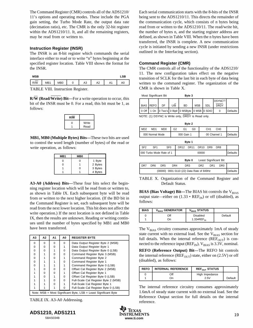
FIGURE 12. ±10V Input Configuration Using VBIAS.
The circuitry which generates the +2.5V reference can bedisabled via the Command Register and will result in a lowerpower dissipation. The reference circuitry consumes a little over1.6mA of current with no external load. When the ADS1210/11is in its default state, the internal reference is enabled.
VBIAS
The VBIAS output voltage is dependent on the reference input(REFIN) voltage and is approximately 1.33 times as great.This output is used to bias input signals such that bipolarsignals with spans of greater than 5V can be scaled to matchthe input range of the ADS1210/11. Figure 12 shows aconnection diagram which will allow the ADS1210/11 toaccept a ±10V input signal (40V full-scale range).
This method of scaling and offsetting the ±20V differentialinput signal will be a concern for those requiring minimumpower dissipation. VBIAS will supply 1.68mA for every chan-nel connected as shown. For the ADS1211, the current drawis within the specifications for VBIAS, but, at 12mW, thepower dissipation is significant. If this is a concern, resistorsR1 and R2 can be set to 9kΩ and R3 and R4 to 3kΩ. This willreduce power dissipation by one-third. In addition, theseresistors can also be set to values which will provide anyarbitrary input range. In all cases, the maximum current intoor out of VBIAS should not exceed its specification of 10mA.
Note that the connection diagram shown in Figure 12 causesa constant amount of current to be sourced by VBIAS. Thiswill be very important in higher resolution designs as thevoltage at VBIAS will not change with loading, as the load isconstant. However, if the input signal is single-ended and oneside of the input is grounded, the load will not be constant andVBIAS will change slightly with the input signal. Also, in allcases, note that noise on VBIAS introduces a common-modeerror signal which is rejected by the converter.
The 3k resistors should not be used as part of an anti-aliasfilter with a capacitor across the inputs. The ADS1210samples charge from the capacitor which has the effect ofintroducing an offset in the measurement. This might beacceptable for relative differential measurements.
The circuitry to generate VBIAS is disabled when theADS1210/11 is in its default state, and it must be enabled,via the Command Register, in order for the VBIAS voltage to
be present. When enabled, the VBIAS circuitry consumesapproximately 1mA with no external load.
On power-up, external signals may be present before VBIASis enabled. This can create a situation in which a negativevoltage is applied to the analog inputs (–2.5V for the circuitshown in Figure 12), reverse biasing the negative inputprotection diode. This situation should not be a problem aslong as the resistors R1 and R2 limit the current beingsourced by each analog input to under 10mA (a potential of0V at the analog input pin should be used in the calculation).
DIGITAL OPERATIONSYSTEM CONFIGURATIONThe Micro Controller (MC) consists of an ALU and aregister bank. The MC has two states: power-on reset andconvert. In the power-on reset state, the MC resets all theregisters to their default state, sets up the modulator to astable state, and performs self-calibration at a 850Hz datarate. After this, it enters the convert mode, which is thenormal mode of operation for the ADS1210/11.
The ADS1210/11 has 5 internal registers, as shown in TableVII. Two of these, the Instruction Register and the Com-mand Register, control the operation of the converter. TheData Output Register (DOR) contains the result from themost recent conversion. The Offset and Full-Scale Calibra-tion Registers (OCR and FCR) contain data used for correct-ing the internal conversion result before it is placed into theDOR. The data in these two registers may be the result of acalibration routine, or they may be values which have beenwritten directly via the serial interface.
TABLE VII. ADS1210/11 Registers.
INSR Instruction Register 8 BitsDOR Data Output Register 24 BitsCMR Command Register 32 BitsOCR Offset Calibration Register 24 BitsFCR Full-Scale Calibration Register 24 Bits
Communication with the ADS1210/11 is controlled via theInstruction Register (INSR). Under normal operation, the INSRis written as the first part of each serial communication. Theinstruction that is sent determines what type of communicationwill occur next. It is not possible to read the INSR.
ADS1210, ADS1211 19SBAS034B www.ti.com
The Command Register (CMR) controls all of the ADS1210/11’s options and operating modes. These include the PGAgain setting, the Turbo Mode Rate, the output data rate(decimation ratio), etc. The CMR is the only 32-bit registerwithin the ADS1210/11. It, and all the remaining registers,may be read from or written to.
Instruction Register (INSR)The INSR is an 8-bit register which commands the serialinterface either to read or to write “n” bytes beginning at thespecified register location. Table VIII shows the format forthe INSR.
Each serial communication starts with the 8-bits of the INSRbeing sent to the ADS1210/11. This directs the remainder ofthe communication cycle, which consists of n bytes beingread from or written to the ADS1210/11. The read/write bit,the number of bytes n, and the starting register address aredefined, as shown in Table VIII. When the n bytes have beentransferred, the INSR is complete. A new communicationcycle is initiated by sending a new INSR (under restrictionsoutlined in the Interfacing section).
Command Register (CMR)The CMR controls all of the functionality of the ADS1210/11. The new configuration takes effect on the negativetransition of SCLK for the last bit in each byte of data beingwritten to the command register. The organization of theCMR is shown in Table X.
The internal reference circuitry consumes approximately1.6mA of steady state current with no external load. See theReference Output section for full details on the internalreference.
TABLE VIII. Instruction Register.
R/W (Read/Write) Bit—For a write operation to occur, thisbit of the INSR must be 0. For a read, this bit must be 1, asfollows:
MB1, MB0 (Multiple Bytes) Bits—These two bits are usedto control the word length (number of bytes) of the read orwrite operation, as follows:
A3-A0 (Address) Bits—These four bits select the begin-ning register location which will be read from or written to,as shown in Table IX. Each subsequent byte will be readfrom or written to the next higher location. (If the BD bit inthe Command Register is set, each subsequent byte will beread from the next lower location. This bit does not affect thewrite operation.) If the next location is not defined in TableIX, then the results are unknown. Reading or writing contin-ues until the number of bytes specified by MB1 and MB0have been transferred.
A3 A2 A1 A0 REGISTER BYTE
0 0 0 0 Data Output Register Byte 2 (MSB)0 0 0 1 Data Output Register Byte 10 0 1 0 Data Output Register Byte 0 (LSB)0 1 0 0 Command Register Byte 3 (MSB)0 1 0 1 Command Register Byte 20 1 1 0 Command Register Byte 10 1 1 1 Command Register Byte 0 (LSB)1 0 0 0 Offset Cal Register Byte 2 (MSB)1 0 0 1 Offset Cal Register Byte 11 0 1 0 Offset Cal Register Byte 0 (LSB)1 1 0 0 Full-Scale Cal Register Byte 2 (MSB)1 1 0 1 Full-Scale Cal Register Byte 11 1 1 0 Full-Scale Cal Register Byte 0 (LSB)
Note: MSB = Most Significant Byte, LSB = Least Significant Byte
R/W
0 Write1 Read
MB1 MB0
0 0 1 Byte0 1 2 Bytes1 0 3 Bytes1 1 4 Bytes
TABLE IX. A3-A0 Addressing.
MSB LSB
R/W MB1 MB0 0 A3 A2 A1 A0
The VBIAS circuitry consumes approximately 1mA of steadystate current with no external load. See the VBIAS section forfull details. When the internal reference (REFOUT) is con-nected to the reference input (REFIN), VBIAS is 3.3V, nominal.
REFO (Reference Output) Bit—The REFO bit controlsthe internal reference (REFOUT) state, either on (2.5V) or off(disabled), as follows:
REFO INTERNAL REFERENCE REFOUT STATUS
0 Off High Impedance1 On 2.5V Default
BIAS (Bias Voltage) Bit—The BIAS bit controls the VBIASoutput state—either on (1.33 • REFIN) or off (disabled), asfollows:
BIAS VBIAS GENERATOR VBIAS STATUS
0 Off Disabled Default1 On 1.33•REFIN
Most Significant Bit Byte 3
DSYNC(1)
BIAS REFO DF U/B BD MSB SDL DRDY
0 Off 1 On 0 Two’s 0 Biplr 0 MSByte 0 MSB 0 SDIO 0 Defaults
NOTE: (1) DSYNC is Write only, DRDY is Read only.
Byte 2
MD2 MD1 MD0 G2 G1 G0 CH1 CH0
000 Normal Mode 000 Gain 1 00 Channel 1 Defaults
Byte 1
SF2 SF1 SF0 DR12 DR11 DR10 DR9 DR8
000 Turbo Mode Rate of 1 00000 Defaults
Byte 0 Least Significant Bit
DR7 DR6 DR5 DR4 DR3 DR2 DR1 DR0
(00000) 0001 0110 (22) Data Rate of 849Hz Defaults
TABLE X. Organization of the Command Register andDefault Status.
ADS1210, ADS121120SBAS034Bwww.ti.com
DF (Data Format) Bit—The DF bit controls the format ofthe output data, either Two’s Complement or Offset Binary,as follows:
DF FORMAT ANALOG INPUT DIGITAL OUTPUT
0 Two’s +Full-Scale 7FFFFFH DefaultComplement Zero 000000H
–Full-Scale 800000H
1 Offset Binary +Full-Scale FFFFFFH
Zero 800000H
–Full-scale 000000H
These two formats are the same for all bits except the mostsignificant, which is simply inverted in one format vs theother. This bit only applies to the Data Output Register—ithas no effect on the other registers.
U/B (Unipolar) Bit—The U/B bit controls the limits im-posed on the output data, as follows:
U/B MODE LIMITS
0 Bipolar None Default1 Unipolar Zero to +Full-Scale only
The particular mode has no effect on the actual full-scalerange of the ADS1210/11, data format, or data format vsinput voltage. In the bipolar mode, the ADS1210/11 oper-ates normally. In the unipolar mode, the conversion result islimited to positive values only (zero included).
This bit only controls what is placed in the Data OutputRegister. It has no effect on internal data. When cleared, thevery next conversion will produce a valid bipolar result.
BD (Byte Order) Bit—The BD bit controls the order inwhich bytes of data are read, either most significant bytefirst or least significant byte, as follows:
SDL (Serial Data Line) Bit—The SDL bit controls whichpin on the ADS1210/11 will be used as the serial data outputpin, either SDIO or SDOUT, as follows:
The MSB bit only affects read operations; it has no effect onwrite operations.
SDL SERIAL DATA OUTPUT PIN
0 SDIO Default1 SDOUT
If SDL is LOW, then SDIO will be used for both input andoutput of serial data—see the Timing section for moredetails on how the SDIO pin transitions between these twostates. In addition, SDOUT will remain in a tri-state condi-tion at all times.
Important Note: Since the default condition is SDL LOW,SDIO has the potential of becoming an output once everydata output cycle if the ADS1210/11 is in the Master Mode.This will occur until the Command Register can be writtenand the SDL bit set HIGH. See the Interfacing section formore information.
DRDY (Data Ready) Bit—The DRDY bit is a read-only bitwhich reflects the state of the ADS1210/11’s DRDY outputpin, as follows:
DRDY MEANING0 Data Ready1 Data Not Ready
DSYNC (Data Synchronization) Bit—The DSYNC bit isa write-only bit which occupies the same location as DRDY.When a ‘one’ is written to this location, the effect on theADS1210/11 is the same as if the DSYNC input pin hadbeen taken LOW and returned HIGH. That is, the modulatorcount for the current conversion cycle will be reset to zero.
The DSYNC bit is provided in order to reduce the number ofinterface signals that are needed between the ADS1210/11and the main controller. Consult “Making Use of DSYNC”in the Serial Interface section for more information.
MD2-MD0 (Operating Mode) Bits—The MD2-MD0 bitsinitiate or enable the various calibration sequences, as follows:
DSYNC MEANING
0 No Change in Modulator Count1 Modulator Count Reset to Zero
MD2 MD1 MD0 OPERATING MODE
0 0 0 Normal Mode0 0 1 Self-Calibration0 1 0 System Offset Calibration0 1 1 System Full-Scale Calibration1 0 0 Pseudo System Calibration1 0 1 Background Calibration1 1 0 Sleep1 1 1 Reserved
The Normal Mode, Background Calibration Mode, andSleep Mode are permanent modes and the ADS1210/11 willremain in these modes indefinitely. All other modes aretemporary and will revert to Normal Mode once the appro-priate actions are complete. See the Calibration and SleepMode sections for more information.
BD BYTE ACCESS ORDER
0 Most Significant Defaultto Least Significant Byte
1 Least Significantto Most Significant Byte
Note that when BD is clear and a multi-byte read is initiated,A3-A0 of the Instruction Register is the address of the mostsignificant byte and subsequent bytes reside at higher ad-dresses. If BD is set, then A3-A0 is the address of the leastsignificant byte and subsequent bytes reside at lower ad-dresses. The BD bit only affects read operations; it has noeffect on write operations.
MSB (Bit Order) Bit—The MSB bit controls the order inwhich bits within a byte of data are read, either mostsignificant bit first or least significant bit, as follows:
MSB BIT ORDER
0 Most Significant Bit First Default1 Least Significant Bit First
ADS1210, ADS1211 21SBAS034B www.ti.com
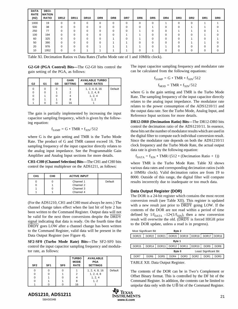
DATA DECI-RATE MATION(HZ) RATIO DR12 DR11 DR10 DR9 DR8 DR7 DR6 DR5 DR4 DR3 DR2 DR1 DR0
1000 19 0 0 0 0 0 0 0 0 1 0 0 1 1500 38 0 0 0 0 0 0 0 1 0 0 1 1 0250 77 0 0 0 0 0 0 1 0 0 1 1 0 1100 194 0 0 0 0 0 1 1 0 0 0 0 1 060 325 0 0 0 0 1 0 1 0 0 0 1 0 150 390 0 0 0 0 1 1 0 0 0 0 1 1 020 976 0 0 0 1 1 1 1 0 1 0 0 0 010 1952 0 0 1 1 1 1 0 1 0 0 0 0 0
Table XI. Decimation Ratios vs Data Rates (Turbo Mode rate of 1 and 10MHz clock).
CH1 CH0 ACTIVE INPUT
0 0 Channel 1 Default0 1 Channel 21 0 Channel 31 1 Channel 4
TURBO AVAILABLEMODE PGA
SF2 SF1 SF0 RATE SETTINGS
0 0 0 1 1, 2, 4, 8, 16 Default0 0 1 2 1, 2, 4, 80 1 0 4 1, 2, 40 1 1 8 1, 21 0 0 16 1
Most Significant Bit Byte 2
DOR23 DOR22 DOR21 DOR20 DOR19 DOR18 DOR17 DOR16
Byte 1
DOR15 DOR14 DOR13 DOR12 DOR11 DOR10 DOR9 DOR8
Byte 0 Least Significant Bit
DOR7 DOR6 DOR5 DOR4 DOR3 DOR2 DOR1 DOR0
TABLE XII. Data Output Register.
G2-G0 (PGA Control) Bits—The G2-G0 bits control thegain setting of the PGA, as follows:
GAIN AVAILABLE TURBOG2 G1 G0 SETTING MODE RATES
0 0 0 1 1, 2, 4, 8, 16 Default0 0 1 2 1, 2, 4, 80 1 0 4 1, 2, 40 1 1 8 1, 21 0 0 16 1
The gain is partially implemented by increasing the inputcapacitor sampling frequency, which is given by the follow-ing equation:
fSAMP = G • TMR • fXIN/512
where G is the gain setting and TMR is the Turbo ModeRate. The product of G and TMR cannot exceed 16. Thesampling frequency of the input capacitor directly relates tothe analog input impedance. See the Programmable GainAmplifier and Analog Input sections for more details.
CH1-CH0 (Channel Selection) Bits—The CH1 and CH0 bitscontrol the input multiplexer on the ADS1211, as follows:
(For the ADS1210, CH1 and CH0 must always be zero.) Thechannel change takes effect when the last bit of byte 2 hasbeen written to the Command Register. Output data will notbe valid for the next three conversions despite the DRDYsignal indicating that data is ready. On the fourth time thatDRDY goes LOW after a channel change has been writtento the Command Register, valid data will be present in theData Output Register (see Figure 4).
SF2-SF0 (Turbo Mode Rate) Bits—The SF2-SF0 bitscontrol the input capacitor sampling frequency and modula-tor rate, as follows:
The input capacitor sampling frequency and modulator ratecan be calculated from the following equations:
fSAMP = G • TMR • fXIN/ 512
fMOD = TMR • fXIN/512
where G is the gain setting and TMR is the Turbo ModeRate. The sampling frequency of the input capacitor directlyrelates to the analog input impedance. The modulator raterelates to the power consumption of the ADS1210/11 andthe output data rate. See the Turbo Mode, Analog Input, andReference Input sections for more details.
DR12-DR0 (Decimation Ratio) Bits—The DR12-DR0 bitscontrol the decimation ratio of the ADS1210/11. In essence,these bits set the number of modulator results which are used inthe digital filter to compute each individual conversion result.Since the modulator rate depends on both the ADS1210/11clock frequency and the Turbo Mode Rate, the actual outputdata rate is given by the following equation:
fDATA = fXIN • TMR/ (512 • (Decimation Ratio + 1))
where TMR is the Turbo Mode Rate. Table XI showsvarious data rates and corresponding decimation ratios (witha 10MHz clock). Valid decimation ratios are from 19 to8000. Outside of this range, the digital filter will computeresults incorrectly due to inadequate or too much data.
Data Output Register (DOR)The DOR is a 24-bit register which contains the most recentconversion result (see Table XII). This register is updatedwith a new result just prior to DRDY going LOW. If thecontents of the DOR are not read within a period of timedefined by 1/fDATA –12•(1/fXIN), then a new conversionresult will overwrite the old. (DRDY is forced HIGH priorto the DOR update, unless a read is in progress).
The contents of the DOR can be in Two’s Complement orOffset Binary format. This is controlled by the DF bit of theCommand Register. In addition, the contents can be limited tounipolar data only with the U/B bit of the Command Register.
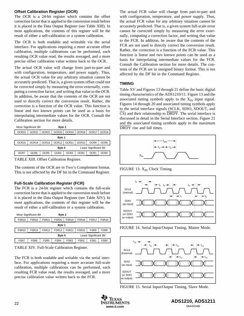
ADS1210, ADS121122SBAS034Bwww.ti.com
Offset Calibration Register (OCR)The OCR is a 24-bit register which contains the offsetcorrection factor that is applied to the conversion result beforeit is placed in the Data Output Register (see Table XIII). Inmost applications, the contents of this register will be theresult of either a self-calibration or a system calibration.
The OCR is both readable and writeable via the serialinterface. For applications requiring a more accurate offsetcalibration, multiple calibrations can be performed, eachresulting OCR value read, the results averaged, and a moreprecise offset calibration value written back to the OCR.
The actual OCR value will change from part-to-part andwith configuration, temperature, and power supply. Thus,the actual OCR value for any arbitrary situation cannot beaccurately predicted. That is, a given system offset could notbe corrected simply by measuring the error externally, com-puting a correction factor, and writing that value to the OCR.In addition, be aware that the contents of the OCR are notused to directly correct the conversion result. Rather, thecorrection is a function of the OCR value. This function islinear and two known points can be used as a basis forinterpolating intermediate values for the OCR. Consult theCalibration section for more details.
Most Significant Bit Byte 2
OCR23 OCR22 OCR21 OCR20 OCR19 OCR18 OCR17 OCR16
Byte 1
OCR15 OCR14 OCR13 OCR12 OCR11 OCR10 OCR9 OCR8
Byte 0 Least Significant Bit
OCR7 OCR6 OCR5 OCR4 OCR3 OCR2 OCR1 OCR0
TABLE XIII. Offset Calibration Register.
The contents of the OCR are in Two’s Complement format.This is not affected by the DF bit in the Command Register.
Full-Scale Calibration Register (FCR)The FCR is a 24-bit register which contains the full-scalecorrection factor that is applied to the conversion result beforeit is placed in the Data Output Register (see Table XIV). Inmost applications, the contents of this register will be theresult of either a self-calibration or a system calibration.
TABLE XIV. Full-Scale Calibration Register.
Most Significant Bit Byte 2
FSR23 FSR22 FSR21 FSR20 FSR19 FSR18 FSR17 FSR16
Byte 1
FSR15 FSR14 FSR13 FSR12 FSR11 FSR10 FSR9 FSR8
Byte 0 Least Significant Bit
FSR7 FSR6 FSR5 FSR4 FSR3 FSR2 FSR1 FSR0
The FCR is both readable and writable via the serial inter-face. For applications requiring a more accurate full-scalecalibration, multiple calibrations can be performed, eachresulting FCR value read, the results averaged, and a moreprecise calibration value written back to the FCR.
The actual FCR value will change from part-to-part andwith configuration, temperature, and power supply. Thus,the actual FCR value for any arbitrary situation cannot beaccurately predicted. That is, a given system full-scale errorcannot be corrected simply by measuring the error exter-nally, computing a correction factor, and writing that valueto the FCR. In addition, be aware that the contents of theFCR are not used to directly correct the conversion result.Rather, the correction is a function of the FCR value. Thisfunction is linear and two known points can be used as abasis for interpolating intermediate values for the FCR.Consult the Calibration section for more details. The con-tents of the FCR are in unsigned binary format. This is notaffected by the DF bit in the Command Register.
TIMING
Table XV and Figures 13 through 21 define the basic digitaltiming characteristics of the ADS1210/11. Figure 13 and theassociated timing symbols apply to the XIN input signal.Figures 14 through 20 and associated timing symbols applyto the serial interface signals (SCLK, SDIO, SDOUT, andCS) and their relationship to DRDY. The serial interface isdiscussed in detail in the Serial Interface section. Figure 21and the associated timing symbols apply to the maximumDRDY rise and fall times.
FIGURE 13. XIN Clock Timing.
tXIN
t2
XIN
t3
FIGURE 14. Serial Input/Output Timing, Master Mode.
FIGURE 15. Serial Input/Output Timing, Slave Mode.
t10
t11 t12 t14
t13 t15
SCLK(External)
SDIO(as input)
SDOUT(or SDlO
as output)
t4t5 t6 t8
t7 t9
SCLK(Internal)
SDIO(as input)
SDOUT(or SDlO
as output)
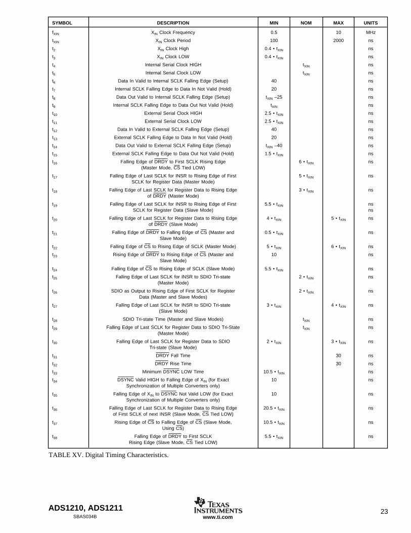
ADS1210, ADS1211 23SBAS034B www.ti.com
TABLE XV. Digital Timing Characteristics.
SYMBOL DESCRIPTION MIN NOM MAX UNITS
fXIN XIN Clock Frequency 0.5 10 MHz
tXIN XIN Clock Period 100 2000 ns
t2 XIN Clock High 0.4 • tXIN ns
t3 XIN Clock LOW 0.4 • tXIN ns
t4 Internal Serial Clock HIGH tXIN ns
t5 Internal Serial Clock LOW tXIN ns
t6 Data In Valid to Internal SCLK Falling Edge (Setup) 40 ns
t7 Internal SCLK Falling Edge to Data In Not Valid (Hold) 20 ns
t8 Data Out Valid to Internal SCLK Falling Edge (Setup) tXIN –25 ns
t9 Internal SCLK Falling Edge to Data Out Not Valid (Hold) tXIN ns
t10 External Serial Clock HIGH 2.5 • tXIN ns
t11 External Serial Clock LOW 2.5 • tXIN ns
t12 Data In Valid to External SCLK Falling Edge (Setup) 40 ns
t13 External SCLK Falling Edge to Data In Not Valid (Hold) 20 ns
t14 Data Out Valid to External SCLK Falling Edge (Setup) tXIN –40 ns
t15 External SCLK Falling Edge to Data Out Not Valid (Hold) 1.5 • tXIN ns
t16 Falling Edge of DRDY to First SCLK Rising Edge 6 • tXIN ns(Master Mode, CS Tied LOW)
t17 Falling Edge of Last SCLK for INSR to Rising Edge of First 5 • tXIN nsSCLK for Register Data (Master Mode)
t18 Falling Edge of Last SCLK for Register Data to Rising Edge 3 • tXIN nsof DRDY (Master Mode)
t19 Falling Edge of Last SCLK for INSR to Rising Edge of First 5.5 • tXIN nsSCLK for Register Data (Slave Mode) ns
t20 Falling Edge of Last SCLK for Register Data to Rising Edge 4 • tXIN 5 • tXIN nsof DRDY (Slave Mode)
t21 Falling Edge of DRDY to Falling Edge of CS (Master and 0.5 • tXIN nsSlave Mode)
t22 Falling Edge of CS to Rising Edge of SCLK (Master Mode) 5 • tXIN 6 • tXIN ns
t23 Rising Edge of DRDY to Rising Edge of CS (Master and 10 nsSlave Mode)
t24 Falling Edge of CS to Rising Edge of SCLK (Slave Mode) 5.5 • tXIN ns
t25 Falling Edge of Last SCLK for INSR to SDIO Tri-state 2 • tXIN ns(Master Mode)
t26 SDIO as Output to Rising Edge of First SCLK for Register 2 • tXIN nsData (Master and Slave Modes)
t27 Falling Edge of Last SCLK for INSR to SDIO Tri-state 3 • tXIN 4 • tXIN ns(Slave Mode)
t28 SDIO Tri-state Time (Master and Slave Modes) tXIN ns
t29 Falling Edge of Last SCLK for Register Data to SDIO Tri-State tXIN ns(Master Mode)
t30 Falling Edge of Last SCLK for Register Data to SDIO 2 • tXIN 3 • tXIN nsTri-state (Slave Mode)
t31 DRDY Fall Time 30 ns
t32 DRDY Rise Time 30 ns
t33 Minimum DSYNC LOW Time 10.5 • tXIN ns
t34 DSYNC Valid HIGH to Falling Edge of XIN (for Exact 10 nsSynchronization of Multiple Converters only)
t35 Falling Edge of XIN to DSYNC Not Valid LOW (for Exact 10 nsSynchronization of Multiple Converters only)
t36 Falling Edge of Last SCLK for Register Data to Rising Edge 20.5 • tXIN nsof First SCLK of next INSR (Slave Mode, CS Tied LOW)
t37 Rising Edge of CS to Falling Edge of CS (Slave Mode, 10.5 • tXIN nsUsing CS)
t38 Falling Edge of DRDY to First SCLK 5.5 • tXIN nsRising Edge (Slave Mode, CS Tied LOW)
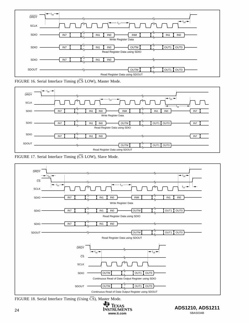
ADS1210, ADS121124SBAS034Bwww.ti.com
FIGURE 17. Serial Interface Timing (CS LOW), Slave Mode.
FIGURE 16. Serial Interface Timing (CS LOW), Master Mode.
t21
DRDY
CS
SCLK
SDIO
t23
IN0IN1IN0IN1IN7 INM
t22 t17
Write Register Data
t18
SDIO OUT0OUT1IN0IN1IN7 OUTM
Read Register Data using SDIO
SDIO IN0IN1IN7
SDOUT OUT0OUT1OUTM
Read Register Data using SDOUT
DRDY
CS
SCLK
SDIO OUT0OUT1OUTM
Continuous Read of Data Output Register using SDIO
Continuous Read of Data Output Register using SDOUT
t18t16
SDOUT OUT0OUT1OUTM
FIGURE 18. Serial Interface Timing (Using CS), Master Mode.
t16
t17t18
IN7 IN1 IN0 INM IN1 IN0
IN7 IN1 IN0 OUTM OUT1 OUT0
Write Register Data
OUTM OUT1 OUT0
IN7 IN1 IN0
Read Register Data using SDIO
Read Register Data using SDOUT
DRDY
SCLK
SDIO
SDIO
SDIO
SDOUT
t20
t36
t38
t19
IN7IN0IN1INMIN1 IN0IN7
Write Register Data
OUT0OUT1OUTM
Read Register Data using SDOUT
IN7
IN7
OUT0OUT1OUTMIN1 IN0IN7
IN1 IN0IN7
Read Register Data using SDIO
DRDY
SCLK
SDIO
SDIO
SDIO
SDOUT
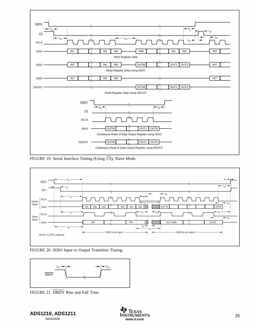
ADS1210, ADS1211 25SBAS034B www.ti.com
OUT M OUT0
OUT MSB OUT0
t26
t16
t22
t24
t38 t19
SDIO is an input SDIO is an output
t28
t21
IN7
IN7 IN6
t23
t18
t29
t20
t30
t27
t17
t25
t26
IN5 IN2 IN1 IN0
IN0
DRDY
CS(1)
SDIO
SCLK
SCLK
SDIO
MasterMode
SlaveMode
NOTE: (1) CS is optional.
FIGURE 19. Serial Interface Timing (Using CS), Slave Mode.
t21
DRDY
CS
SCLK
SDIO
t37
t23
t24
IN7IN0IN1IN0IN1IN7 INM
t24 t19
Write Register Data
t20
SDIO IN7OUT0OUT1IN0IN1IN7 OUTM
Read Register Data Using SDIO
SDIO IN7IN0IN1IN7
SDOUT OUT0OUT1OUTM
Read Register Data Using SDOUT
DRDY
CS
SCLK
SDIO OUT0OUT1OUTM
Continuous Read of Data Output Register using SDIO
Continuous Read of Data Output Register using SDOUT
t20t16
SDOUT OUT0OUT1OUTM
FIGURE 20. SDIO Input to Output Transition Timing.
FIGURE 21. DRDY Rise and Fall Time.
t31 t32
DRDY
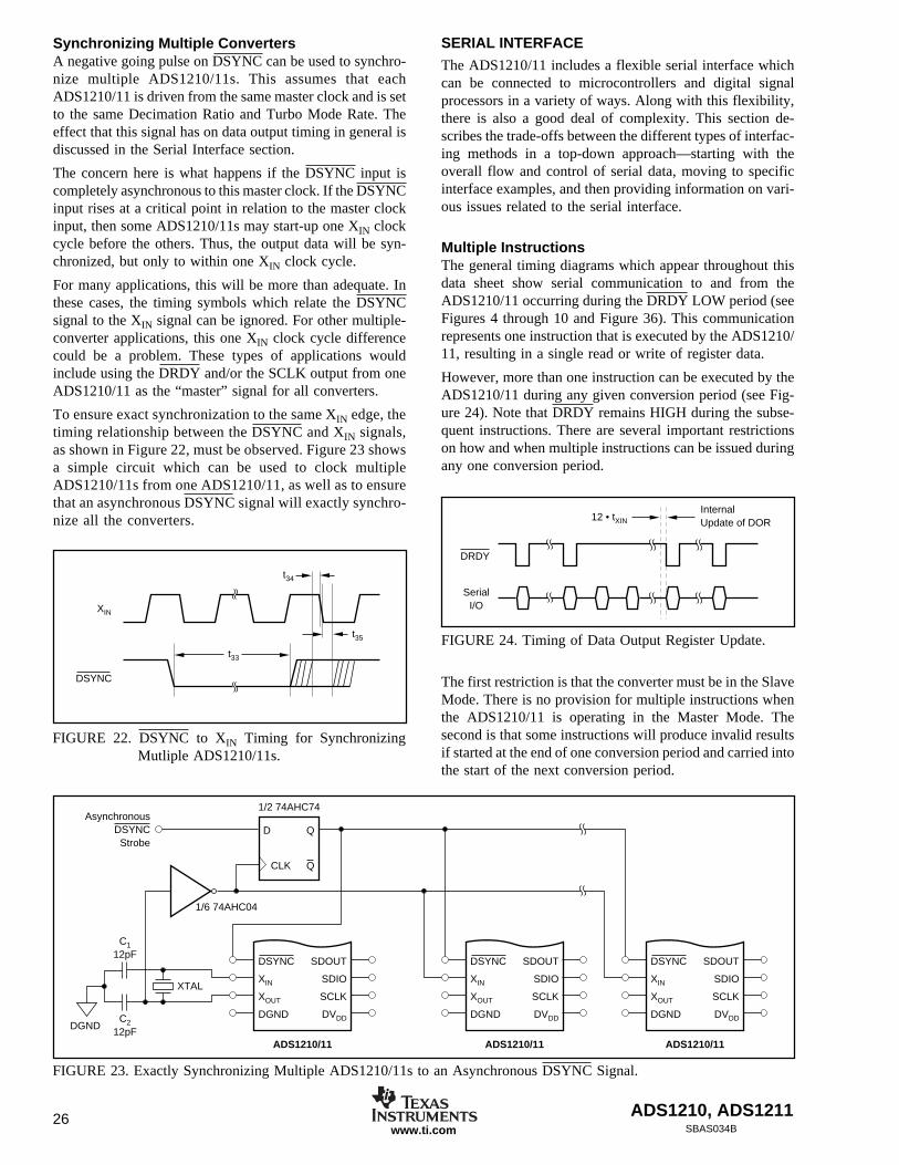
ADS1210, ADS121126SBAS034Bwww.ti.com
Synchronizing Multiple ConvertersA negative going pulse on DSYNC can be used to synchro-nize multiple ADS1210/11s. This assumes that eachADS1210/11 is driven from the same master clock and is setto the same Decimation Ratio and Turbo Mode Rate. Theeffect that this signal has on data output timing in general isdiscussed in the Serial Interface section.
The concern here is what happens if the DSYNC input iscompletely asynchronous to this master clock. If the DSYNCinput rises at a critical point in relation to the master clockinput, then some ADS1210/11s may start-up one XIN clockcycle before the others. Thus, the output data will be syn-chronized, but only to within one XIN clock cycle.
For many applications, this will be more than adequate. Inthese cases, the timing symbols which relate the DSYNCsignal to the XIN signal can be ignored. For other multiple-converter applications, this one XIN clock cycle differencecould be a problem. These types of applications wouldinclude using the DRDY and/or the SCLK output from oneADS1210/11 as the “master” signal for all converters.
To ensure exact synchronization to the same XIN edge, thetiming relationship between the DSYNC and XIN signals,as shown in Figure 22, must be observed. Figure 23 showsa simple circuit which can be used to clock multipleADS1210/11s from one ADS1210/11, as well as to ensurethat an asynchronous DSYNC signal will exactly synchro-nize all the converters.
FIGURE 22. DSYNC to XIN Timing for SynchronizingMutliple ADS1210/11s.
SERIAL INTERFACE
The ADS1210/11 includes a flexible serial interface whichcan be connected to microcontrollers and digital signalprocessors in a variety of ways. Along with this flexibility,there is also a good deal of complexity. This section de-scribes the trade-offs between the different types of interfac-ing methods in a top-down approach—starting with theoverall flow and control of serial data, moving to specificinterface examples, and then providing information on vari-ous issues related to the serial interface.
Multiple InstructionsThe general timing diagrams which appear throughout thisdata sheet show serial communication to and from theADS1210/11 occurring during the DRDY LOW period (seeFigures 4 through 10 and Figure 36). This communicationrepresents one instruction that is executed by the ADS1210/11, resulting in a single read or write of register data.
However, more than one instruction can be executed by theADS1210/11 during any given conversion period (see Fig-ure 24). Note that DRDY remains HIGH during the subse-quent instructions. There are several important restrictionson how and when multiple instructions can be issued duringany one conversion period.
DRDY
SerialI/O
12 • tXINInternalUpdate of DOR
FIGURE 24. Timing of Data Output Register Update.
The first restriction is that the converter must be in the SlaveMode. There is no provision for multiple instructions whenthe ADS1210/11 is operating in the Master Mode. Thesecond is that some instructions will produce invalid resultsif started at the end of one conversion period and carried intothe start of the next conversion period.
FIGURE 23. Exactly Synchronizing Multiple ADS1210/11s to an Asynchronous DSYNC Signal.
t33
t34
t35
XIN
DSYNC
C212pF
C112pF
XTAL
DSYNC
XIN
XOUT
DGND
ADS1210/11
SDOUT
SDIO
SCLK
DVDD
D
CLK
1/2 74AHC74
1/6 74AHC04
Q
Q
DSYNC
XIN
XOUT
DGND
ADS1210/11
SDOUT
SDIO
SCLK
DVDD
DSYNC
XIN
XOUT
DGND
ADS1210/11
SDOUT
SDIO
SCLK
DVDD
AsynchronousDSYNCStrobe
DGND
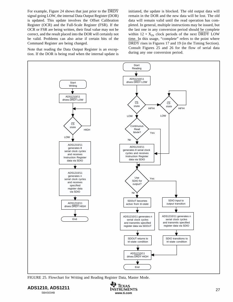
ADS1210, ADS1211 27SBAS034B www.ti.com
StartWriting
ADS1210/11drives DRDY LOW
CSstate
ADS1210/11generates 8
serial clock cyclesand receives
Instruction Registerdata via SDIO
ADS1210/11generates n
serial clock cyclesand receives
specifiedregister data
via SDIO
ADS1210/11drives DRDY HIGH
End
ADS1210/11generates 8 serial clock
cycles and receivesInstruction Register
data via SDIO
ADS1210/11 generates nserial clock cycles
and transmits specifiedregister data via SDOUT
End
StartReading
ADS1210/11drives DRDY LOW
CSstate
ContinuousRead
Mode?
ADS1210/11drives DRDY HIGH
SDOUT returns totri-state condition
SDOUT becomesactive from tri-state
UseSDIO foroutput?
HIGH
No
Yes
LOW
HIGH
No
Yes
ADS1210/11 generates nserial clock cycles
and transmits specifiedregister data via SDIO
SDIO transitions totri-state condition
SDIO input tooutput transition
CS state
LOW LOW
HIGH
For example, Figure 24 shows that just prior to the DRDYsignal going LOW, the internal Data Output Register (DOR)is updated. This update involves the Offset CalibrationRegister (OCR) and the Full-Scale Register (FSR). If theOCR or FSR are being written, their final value may not becorrect, and the result placed into the DOR will certainly notbe valid. Problems can also arise if certain bits of theCommand Register are being changed.
Note that reading the Data Output Register is an excep-tion. If the DOR is being read when the internal update is
initiated, the update is blocked. The old output data willremain in the DOR and the new data will be lost. The olddata will remain valid until the read operation has com-pleted. In general, multiple instructions may be issued, butthe last one in any conversion period should be completewithin 12 • XIN clock periods of the next DRDY LOWtime. In this usage, “complete” refers to the point whereDRDY rises in Figures 17 and 19 (in the Timing Section).Consult Figures 25 and 26 for the flow of serial dataduring any one conversion period.
FIGURE 25. Flowchart for Writing and Reading Register Data, Master Mode.
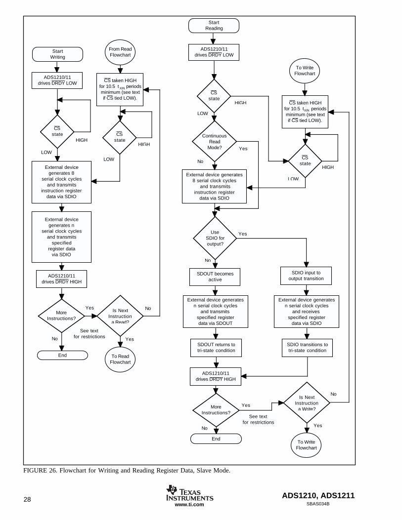
ADS1210, ADS121128SBAS034Bwww.ti.com
StartWriting
ADS1210/11drives DRDY LOW
CSstate
External devicegenerates 8
serial clock cyclesand transmits
instruction registerdata via SDIO
External devicegenerates n
serial clock cyclesand transmits
specifiedregister data
via SDIO
ADS1210/11drives DRDY HIGH
End
External device generates8 serial clock cycles
and receives instruction register
data via SDIO
External device generatesn serial clock cycles
and transmits specified registerdata via SDOUT
End
StartReading
ADS1210/11drives DRDY LOW
CSstate
ContinuousRead
Mode?
ADS1210/11drives DRDY HIGH
SDOUT returns totri-state condition
SDOUT becomesactive
UseSDIO foroutput?
LOW
HIGH
No
YesLOW
No
Yes
External device generatesn serial clock cycles
and receives specified register
data via SDIO
SDIO transitions totri-state condition
SDIO input tooutput transition
MoreInstructions?
No
Yes Is NextInstruction
a Read?
To ReadFlowchart
From ReadFlowchart
CS taken HIGHfor 10.5 t periodsminimum (see textif CS tied LOW).
CSstate
HIGH
MoreInstructions?
No
Is NextInstruction
a Write?
To WriteFlowchart
Yes
See textfor restrictions
Yes
To WriteFlowchart
CS taken HIGHfor 10.5 t periodsminimum (see textif CS tied LOW).
CSstate
LOW
HIGH
No
See textfor restrictions Yes
No
LOW
HIGH
FIGURE 26. Flowchart for Writing and Reading Register Data, Slave Mode.
XIN
XIN
transmits
ADS1210, ADS1211 29SBAS034B www.ti.com
The recommended solution to this problem is to actively pullSDIO LOW. If SDIO is LOW when the ADS1210/11 entersthe instruction byte, then the resulting instruction is a writeof one byte of data to the Data Output Register, which resultsin no internal operation.
If the SDIO signal cannot be actively pulled LOW, thenanother possibility is to time the initialization of thecontroller’s serial port such that it becomes active betweenadjacent DRDY LOW periods. The default configuration forthe ADS1210/11 produces a data rate of 814Hz—a conver-sion period of 1.2ms. This time should be more than ad-equate for most microcontrollers and DSPs to monitor DRDYand initialize the serial port at the appropriate time.
Master ModeThe Master Mode is active when the MODE input is HIGH.All serial clock cycles will be produced by the ADS1210/11in this mode, and the SCLK pin is configured as an output.The frequency of the serial clock will be one-half of the XINfrequency. Multiple instructions cannot be issued during asingle conversion period in this mode—only one instructionper conversion cycle is possible.
The Master Mode will be difficult for some microcontrollers,particularly when the XIN input frequency is greater than afew MHz, as the serial clock may exceed the microcontroller’smaximum serial clock frequency. For the majority of digitalsignal processors, this will be much less of a concern. Inaddition, if SDIO is being used as an input and an output,then the transition time from input to output may be aconcern. This will be true for both microcontrollers andDSPs. See Figure 20 in the Timing section.
Note that if CS is tied LOW, there are special considerationsregarding SDIO as outlined previously in this section. Alsonote that if CS is being used to control the flow of data fromthe ADS1210/11 and it remains HIGH for one or moreconversion periods, the ADS1210/11 will operate properly.However, the result in the Data Output Register will be lostwhen it is overwritten by each new result. Just prior to thisupdate, DRDY will be forced HIGH and will return LOWafter the update.
Slave ModeMost systems will use the ADS1210/11 in the Slave Mode.This mode allows multiple instructions to be issued perconversion period as well as allowing the main controller toset the serial clock frequency and pace the serial datatransfer. The ADS1210/11 is in the Slave Mode when theMODE input is LOW.
There are several important items regarding the serial clockfor this mode of operation. The maximum serial clockfrequency cannot exceed the ADS1210/11 XIN frequencydivided by 5 (see Figure 15 in the Timing section).
When using SDIO as the serial output, the falling edge of thelast serial clock cycle of the instruction byte will cause theSDIO pin to begin its transition from input to output.Between three and four XIN cycles after this falling edge, theSDIO pin will become an output. This transition may be toofast for some microcontrollers and digital signal processors.
Using CS and Continuous Read ModeThe serial interface may make use of the CS signal, or thisinput may simply be tied LOW. There are several issuesassociated with choosing to do one or the other.
The CS signal does not directly control the tri-state conditionof the SDOUT or SDIO output. These signals are normallyin the tri-state condition. They only become active whenserial data is being transmitted from the ADS1210/11. If theADS1210/11 is in the middle of a serial transfer and SDOUTor SDIO is an output, taking CS HIGH will not tri-state theoutput signal.
If there are multiple serial peripherals utilizing the sameserial I/O lines and communication may occur with anyperipheral at any time, then the CS signal must be used. TheADS1210/11 may be in the Master Mode or the Slave Mode.In the Master Mode, the CS signal is used to hold-off serialcommunication with a “ready” (DRDY LOW) ADS1210/11until the main controller can accommodate the communica-tion. In the Slave Mode, the CS signal is used to enablecommunication with the ADS1210/11.
The CS input has another use. If the CS state is left LOWafter a read of the Data Output Register has been performed,then the next time that DRDY goes LOW, the ADS1210/11Instruction Register will not be entered. Instead, the Instruc-tion Register contents will be re-used, and the new contentsof the Data Output Register, or some part thereof, will betransmitted. This will occur as long as CS is LOW and nottoggled.
This mode of operation is called the Continuous Read Modeand is shown in the read flowcharts of Figures 25 and 26. Itis also shown in the Timing Diagrams of Figures 18 and 19in the Timing section. Note that once CS has been takenHIGH, the Continuous Read Mode will be enabled (but notentered) and can never be disabled. The mode is actuallyentered and exited as described above.
Power-On Conditions for SDIOEven if the SDIO connection will be used only for input,there is one important item to consider regarding SDIO. Thisonly applies when the ADS1210/11 is in the Master Modeand CS will be tied LOW. At power-up, the serial I/O linesof most microcontrollers and digital signal processors will bein a tri-state condition, or they will be configured as inputs.When power is applied to the ADS1210/11, it will beginoperating as defined by the default condition of the Com-mand Register (see Table X in the System Configurationsection). This condition defines SDIO as the data output pin.
Since the ADS1210/11 is in the Master Mode and CS is tiedLOW, the serial clock will run whenever DRDY is LOW andan instruction will be entered and executed. If the SDIO lineis HIGH, as it might be with an active pull-up, then theinstruction is a read operation and SDIO will become anoutput every DRDY LOW period—for 32 serial clock cycles.When the serial port on the main controller is enabled, signalcontention could result.
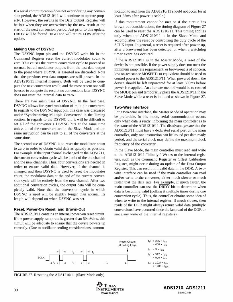
ADS1210, ADS121130SBAS034Bwww.ti.com
If a serial communication does not occur during any conver-sion period, the ADS1210/11 will continue to operate prop-erly. However, the results in the Data Output Register willbe lost when they are overwritten by the new result at thestart of the next conversion period. Just prior to this update,DRDY will be forced HIGH and will return LOW after theupdate.
Making Use of DSYNCThe DSYNC input pin and the DSYNC write bit in theCommand Register reset the current modulator count tozero. This causes the current conversion cycle to proceed asnormal, but all modulator outputs from the last data outputto the point where DSYNC is asserted are discarded. Notethat the previous two data outputs are still present in theADS1210/11 internal memory. Both will be used to com-pute the next conversion result, and the most recent one willbe used to compute the result two conversions later. DSYNCdoes not reset the internal data to zero.
There are two main uses of DSYNC. In the first case,DSYNC allows for synchronization of multiple converters.In regards to the DSYNC input pin, this case was discussedunder “Synchronizing Multiple Converters” in the Timingsection. In regards to the DSYNC bit, it will be difficult toset all of the converter’s DSYNC bits at the same timeunless all of the converters are in the Slave Mode and thesame instruction can be sent to all of the converters at thesame time.
The second use of DSYNC is to reset the modulator countto zero in order to obtain valid data as quickly as possible.For example, if the input channel is changed on the ADS1211,the current conversion cycle will be a mix of the old channeland the new channels. Thus, four conversions are needed inorder to ensure valid data. However, if the channel ischanged and then DSYNC is used to reset the modulatorcount, the modulator data at the end of the current conver-sion cycle will be entirely from the new channel. After twoadditional conversion cycles, the output data will be com-pletely valid. Note that the conversion cycle in whichDSYNC is used will be slightly longer than normal. Itslength will depend on when DSYNC was set.
Reset, Power-On Reset, and Brown-OutThe ADS1210/11 contains an internal power-on reset circuit.If the power supply ramp rate is greater than 50mV/ms, thiscircuit will be adequate to ensure that the device powers upcorrectly. (Due to oscillator settling considerations, commu-
nication to and from the ADS1210/11 should not occur for atleast 25ms after power is stable.)
If this requirement cannot be met or if the circuit hasbrown-out considerations, the timing diagram of Figure 27can be used to reset the ADS1210/11. This timing appliesonly when the ADS1210/11 is in the Slave Mode andaccomplishes the reset by controlling the duty cycle of theSCLK input. In general, a reset is required after power-up,after a brown-out has been detected, or when a watchdogtimer event has occured.
If the ADS1210/11 is in the Master Mode, a reset of thedevice is not possible. If the power supply does not meet theminimum ramp rate requirement, or brown-out is of concern,low on-resistance MOSFETs or equivalent should be used tocontrol power to the ADS1210/11. When powered down, thedevice should be left unpowered for at least 300ms beforepower is reapplied. An alternate method would be to controlthe MODE pin and temporarily place the ADS1210/11 in theSlave Mode while a reset is initiated as shown in Figure 27.
Two-Wire InterfaceFor a two-wire interface, the Master Mode of operation maybe preferable. In this mode, serial communication occursonly when data is ready, informing the main controller as tothe status of the ADS1210/11. The disadvantages are that theADS1210/11 must have a dedicated serial port on the maincontroller, only one instruction can be issued per data readyperiod, and the serial clock may define the maximum clockfrequency of the converter.
In the Slave Mode, the main controller must read and writeto the ADS1210/11 “blindly.” Writes to the internal regis-ters, such as the Command Register or Offset CalibrationRegister, might occur during an update of the Data OutputRegister. This can result in invalid data in the DOR. A two-wire interface can be used if the main controller can readand/or write to the converter, either much slower or muchfaster that the data rate. For example, if much faster, themain controller can use the DRDY bit to determine whendata is becoming valid (polling it multiple times during oneconversion cycle). Thus, the controller obtains some idea ofwhen to write to the internal register. If much slower, thenreads of the DOR might always return valid data (multipleconversions have occurred since the last read of the DOR orsince any write of the internal registers).
FIGURE 27. Resetting the ADS1210/11 (Slave Mode only).
t1: > 256 • tXIN
< 400 • tXIN
t2: > 5 • tXIN
t3: > 512 • tXIN
< 900 • tXIN
t4: ≥ 1024 • tXIN
< 1200 • tXIN
t1 t3 t4
t2 t2
SCLK
Reset Occursat Falling Edge
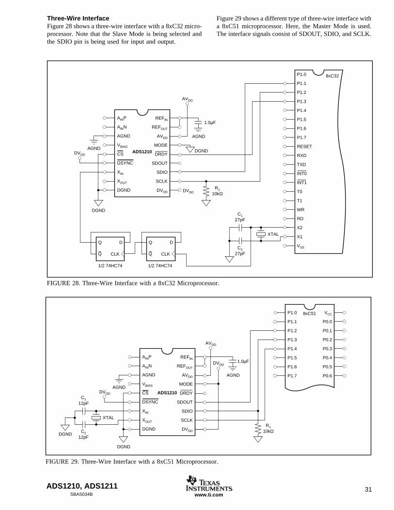
ADS1210, ADS1211 31SBAS034B www.ti.com
FIGURE 29. Three-Wire Interface with a 8xC51 Microprocessor.
Three-Wire InterfaceFigure 28 shows a three-wire interface with a 8xC32 micro-processor. Note that the Slave Mode is being selected andthe SDIO pin is being used for input and output.
ADS1210
AINP
AINN
AGND
VBIAS
CS
DSYNC
XIN
XOUT
DGND
REFIN
REFOUT
AVDD
MODE
DRDY
SDOUT
SDIO
SCLK
DVDD
P1.0
P1.1
P1.2
P1.3
P1.4
P1.5
P1.6
P1.7
VCC
P0.0
P0.1
P0.2
P0.3
P0.4
P0.5
P0.6
8xC51
C212pF
C112pF
DVDD
AGND
DGND
DGND
AVDD
DVDD
XTAL
AGND
1.0µF
R110kΩ
FIGURE 28. Three-Wire Interface with a 8xC32 Microprocessor.
ADS1210
AINP
AINN
AGND
VBIAS
CS
DSYNC
XIN
XOUT
DGND
REFIN
REFOUT
AVDD
MODE
DRDY
SDOUT
SDIO
SCLK
DVDD
P1.0
P1.1
P1.2
P1.3
P1.4
P1.5
P1.6
P1.7
RESET
RXD
TXD
INT0
INT1
T0
T1
WR
RD
X2
X1
VSS
8xC32
C227pF
C127pF
DVDD
AGND DGND
DGND
AVDD
DVDD
D
CLK
Q
Q
D
CLK
Q
Q
1/2 74HC74 1/2 74HC74
XTAL
AGND
1.0µF
R110kΩ
Figure 29 shows a different type of three-wire interface witha 8xC51 microprocessor. Here, the Master Mode is used.The interface signals consist of SDOUT, SDIO, and SCLK.
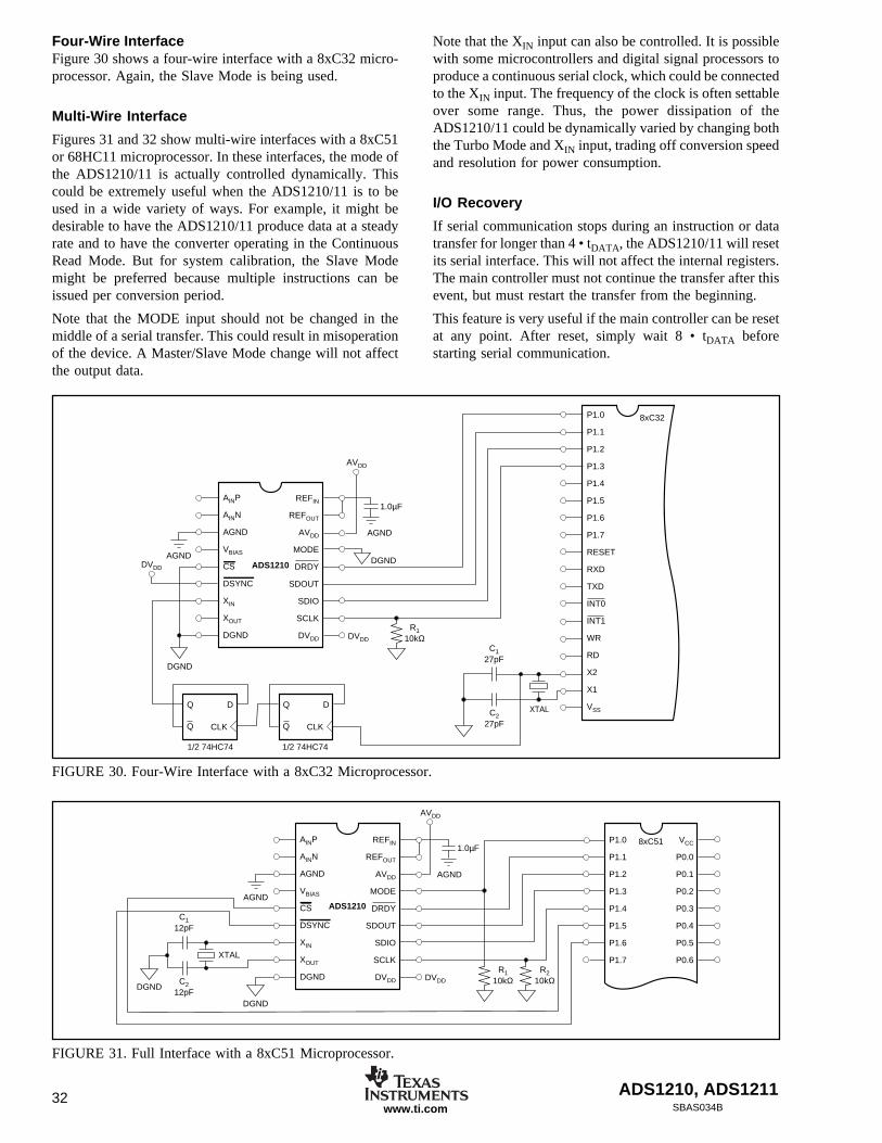
ADS1210, ADS121132SBAS034Bwww.ti.com
Four-Wire InterfaceFigure 30 shows a four-wire interface with a 8xC32 micro-processor. Again, the Slave Mode is being used.
Multi-Wire Interface
Figures 31 and 32 show multi-wire interfaces with a 8xC51or 68HC11 microprocessor. In these interfaces, the mode ofthe ADS1210/11 is actually controlled dynamically. Thiscould be extremely useful when the ADS1210/11 is to beused in a wide variety of ways. For example, it might bedesirable to have the ADS1210/11 produce data at a steadyrate and to have the converter operating in the ContinuousRead Mode. But for system calibration, the Slave Modemight be preferred because multiple instructions can beissued per conversion period.
Note that the MODE input should not be changed in themiddle of a serial transfer. This could result in misoperationof the device. A Master/Slave Mode change will not affectthe output data.
Note that the XIN input can also be controlled. It is possiblewith some microcontrollers and digital signal processors toproduce a continuous serial clock, which could be connectedto the XIN input. The frequency of the clock is often settableover some range. Thus, the power dissipation of theADS1210/11 could be dynamically varied by changing boththe Turbo Mode and XIN input, trading off conversion speedand resolution for power consumption.
I/O Recovery
If serial communication stops during an instruction or datatransfer for longer than 4 • tDATA, the ADS1210/11 will resetits serial interface. This will not affect the internal registers.The main controller must not continue the transfer after thisevent, but must restart the transfer from the beginning.
This feature is very useful if the main controller can be resetat any point. After reset, simply wait 8 • tDATA beforestarting serial communication.
FIGURE 31. Full Interface with a 8xC51 Microprocessor.
FIGURE 30. Four-Wire Interface with a 8xC32 Microprocessor.
ADS1210
AINP
AINN
AGND
VBIAS
CS
DSYNC
XIN
XOUT
DGND
REFIN
REFOUT
AVDD
MODE
DRDY
SDOUT
SDIO
SCLK
DVDD
P1.0
P1.1
P1.2
P1.3
P1.4
P1.5
P1.6
P1.7
VCC
P0.0
P0.1
P0.2
P0.3
P0.4
P0.5
P0.6
8xC51
C212pF
C112pF
XTAL
AGND
DGND
AVDD
DVDD
DGND
AGND
1.0µF
R110kΩ
R210kΩ
ADS1210
AINP
AINN
AGND
VBIAS
CS
DSYNC
XIN
XOUT
DGND
REFIN
REFOUT
AVDD
MODE
DRDY
SDOUT
SDIO
SCLK
DVDD
P1.0
P1.1
P1.2
P1.3
P1.4
P1.5
P1.6
P1.7
RESET
RXD
TXD
INT0
INT1
WR
RD
X2
X1
VSS
8xC32
C227pF
C127pF
DVDD
AGND DGND
DGND
AVDD
DVDD
D
CLK
Q
Q
D
CLK
Q
Q
1/2 74HC74 1/2 74HC74
XTAL
AGND
1.0µF
R110kΩ
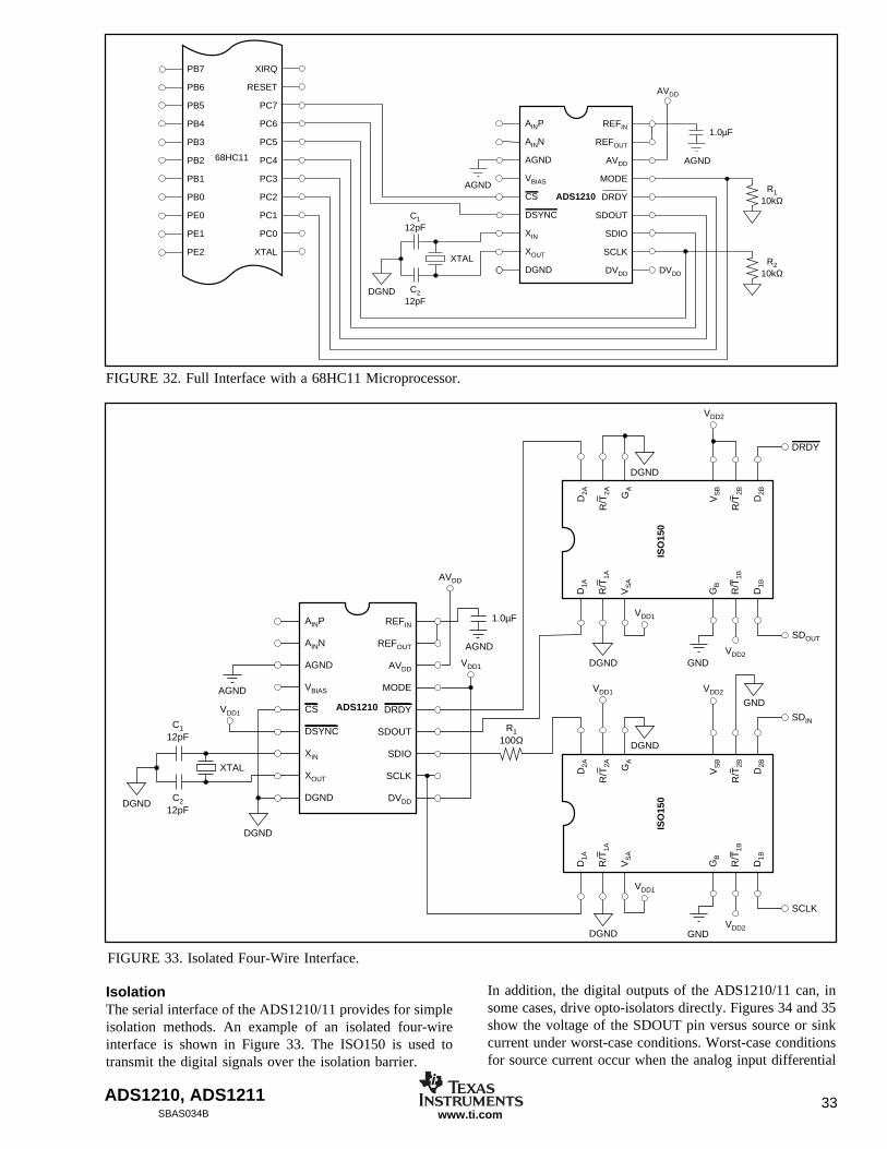
ADS1210, ADS1211 33SBAS034B www.ti.com
FIGURE 32. Full Interface with a 68HC11 Microprocessor.
IsolationThe serial interface of the ADS1210/11 provides for simpleisolation methods. An example of an isolated four-wireinterface is shown in Figure 33. The ISO150 is used totransmit the digital signals over the isolation barrier.
In addition, the digital outputs of the ADS1210/11 can, insome cases, drive opto-isolators directly. Figures 34 and 35show the voltage of the SDOUT pin versus source or sinkcurrent under worst-case conditions. Worst-case conditionsfor source current occur when the analog input differential
FIGURE 33. Isolated Four-Wire Interface.
ADS1210
AINP
AINN
AGND
VBIAS
CS
DSYNC
XIN
XOUT
DGND
REFIN
REFOUT
AVDD
MODE
DRDY
SDOUT
SDIO
SCLK
DVDD
PB7
PB6
PB5
PB4
PB3
PB2
PB1
PB0
PE0
PE1
PE2
XIRQ
RESET
PC7
PC6
PC5
PC4
PC3
PC2
PC1
PC0
XTAL
68HC11
C212pF
C112pF
AGND
DGND
AVDD
DVDD
XTAL
AGND
1.0µF
R110kΩ
R210kΩ
ADS1210
AINP
AINN
AGND
VBIAS
CS
DSYNC
XIN
XOUT
DGND
REFIN
REFOUT
AVDD
MODE
DRDY
SDOUT
SDIO
SCLK
DVDD
XTAL
C212pF
C112pF
VDD1
AGND
DGND
DGND
AVDD
VDD1IS
O15
0
D1A
R/T
1A
VS
A
GB
R/T
1B
D1B
D2A
R/T
2A GA
VS
B
R/T
2B
D2B
VDD2VDD1
VDD1
VDD2
R1100Ω DGND
GND
DGND GND
SCLK
SDIN
VDD2
VDD1
VDD2
DGND
DGND GND
SDOUT
DRDY
ISO
150
D1A
R/T
1A
VS
A
GB
R/T
1B
D1B
D2A
R/T
2A GA
VS
B
R/T
2B
D2B
AGND
1.0µF
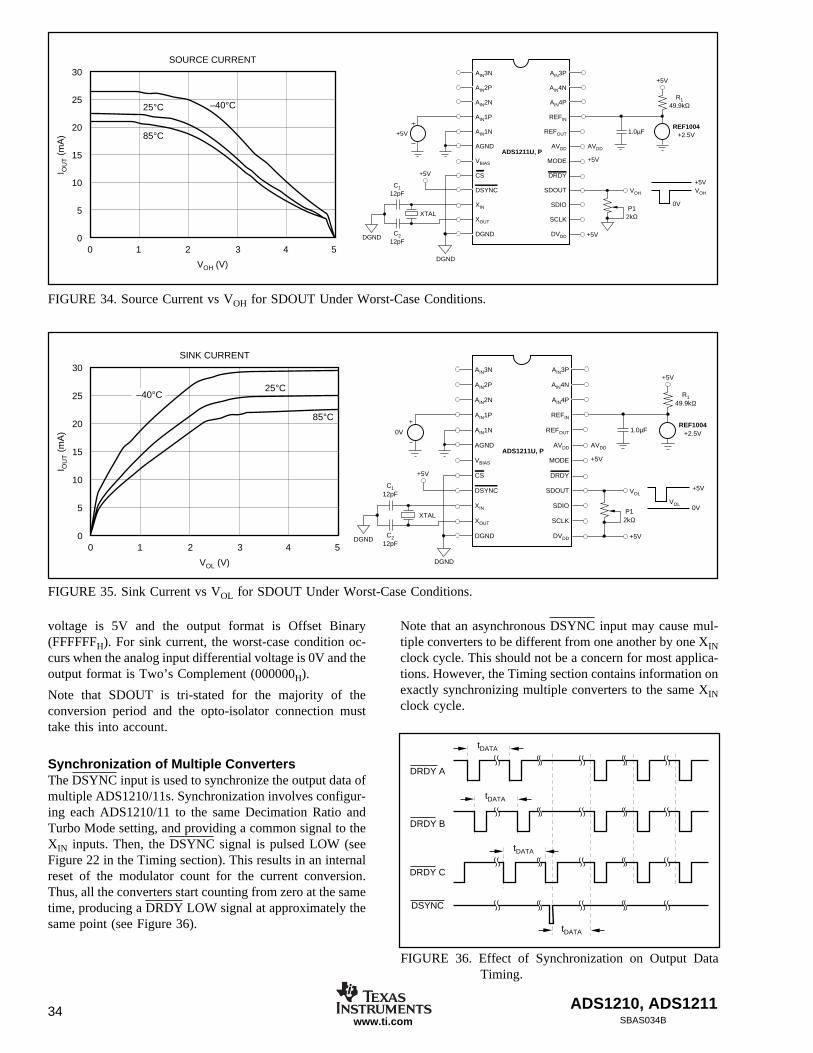
ADS1210, ADS121134SBAS034Bwww.ti.com
ADS1211U, P
AIN3N
AIN2P
AIN2N
AIN1P
AIN1N
AGND
VBIAS
CS
DSYNC
XIN
XOUT
DGND
AIN3P
AIN4N
AIN4P
REFIN
REFOUT
AVDD
MODE
DRDY
SDOUT
SDIO
SCLK
DVDD
AVDD
+5V
+5V
VOL
0VVOL
+5V
R149.9kΩ
C212pF
C112pF
DGND
XTAL
DGND
REF1004+2.5V0V
+5V
P12kΩ
1.0µF
+5V
ADS1211U, P
AIN3N
AIN2P
AIN2N
AIN1P
AIN1N
AGND
VBIAS
CS
DSYNC
XIN
XOUT
DGND
AIN3P
AIN4N
AIN4P
REFIN
REFOUT
AVDD
MODE
DRDY
SDOUT
SDIO
SCLK
DVDD
1.0µF
AVDD
+5V
+5V
+5V
0V
+5V
R149.9kΩ
C212pF
C112pF
XTAL
DGND
DGND
REF1004+2.5V+5V
VOHVOH
P12kΩ
+5V
DRDY A
DRDY B
DRDY C
DSYNC
tDATA
tDATA
tDATA
tDATA
voltage is 5V and the output format is Offset Binary(FFFFFFH). For sink current, the worst-case condition oc-curs when the analog input differential voltage is 0V and theoutput format is Two’s Complement (000000H).
Note that SDOUT is tri-stated for the majority of theconversion period and the opto-isolator connection musttake this into account.
Synchronization of Multiple ConvertersThe DSYNC input is used to synchronize the output data ofmultiple ADS1210/11s. Synchronization involves configur-ing each ADS1210/11 to the same Decimation Ratio andTurbo Mode setting, and providing a common signal to theXIN inputs. Then, the DSYNC signal is pulsed LOW (seeFigure 22 in the Timing section). This results in an internalreset of the modulator count for the current conversion.Thus, all the converters start counting from zero at the sametime, producing a DRDY LOW signal at approximately thesame point (see Figure 36).
Note that an asynchronous DSYNC input may cause mul-tiple converters to be different from one another by one XINclock cycle. This should not be a concern for most applica-tions. However, the Timing section contains information onexactly synchronizing multiple converters to the same XINclock cycle.
FIGURE 36. Effect of Synchronization on Output DataTiming.
FIGURE 35. Sink Current vs VOL for SDOUT Under Worst-Case Conditions.
30
25
20
15
10
5
0
SINK CURRENT
VOL (V)
0 1 2 3 4 5
I OU
T (
mA
)
25°C
85°C
–40°C
FIGURE 34. Source Current vs VOH for SDOUT Under Worst-Case Conditions.
30
25
20
15
10
5
0
SOURCE CURRENT
VOH (V)
0 21 3 4 5
I OU
T (
mA
)
25°C
85°C
–40°C
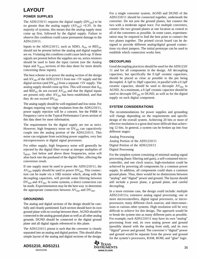
ADS1210, ADS1211 35SBAS034B www.ti.com
LAYOUTPOWER SUPPLIES
The ADS1210/11 requires the digital supply (DVDD) to beno greater than the analog supply (AVDD) +0.3V. In themajority of systems, this means that the analog supply mustcome up first, followed by the digital supply. Failure toobserve this condition could cause permanent damage to theADS1210/11.
Inputs to the ADS1210/11, such as SDIO, AIN, or REFIN,should not be present before the analog and digital suppliesare on. Violating this condition could cause latch-up. If thesesignals are present before the supplies are on, series resistorsshould be used to limit the input current (see the AnalogInput and VBIAS sections of this data sheet for more detailsconcerning these inputs).
The best scheme is to power the analog section of the designand AVDD of the ADS1210/11 from one +5V supply and thedigital section (and DVDD) from a separate +5V supply. Theanalog supply should come up first. This will ensure that AINand REFIN do not exceed AVDD and that the digital inputsare present only after AVDD has been established, and thatthey do not exceed DVDD.
The analog supply should be well-regulated and low-noise. Fordesigns requiring very high resolution from the ADS1210/11,power supply rejection will be a concern. See the PSRR vsFrequency curve in the Typical Performance Curves section ofthis data sheet for more information.
The requirements for the digital supply are not as strict.However, high frequency noise on DVDD can capacitivelycouple into the analog portion of the ADS1210/11. Thisnoise can originate from switching power supplies, very fastmicroprocessors or digital signal processors.
For either supply, high frequency noise will generally berejected by the digital filter except at interger multiplies offMOD. Just below and above these frequencies, noise willalias back into the passband of the digital filter, affecting theconversion result.
If one supply must be used to power the ADS1210/11, theAVDD supply should be used to power DVDD. This connec-tion can be made via a 10Ω resistor which, along with thedecoupling capacitors, will provide some filtering betweenDVDD and AVDD. In some systems, a direct connection canbe made. Experimentation may be the best way to determinethe appropriate connection between AVDD and DVDD.
GROUNDING
The analog and digital sections of the design should be care-fully and cleanly partitioned. Each section should have its ownground plane with no overlap between them. AGND should beconnected to the analog ground plane as well as all other analoggrounds. DGND should be connected to the digital groundplane and all digital signals referenced to this plane.
The ADS1210/11 pinout is such that the converter is cleanlyseparated into an analog and digital portion. This should allowsimple layout of the analog and digital sections of the design.
For a single converter system, AGND and DGND of theADS1210/11 should be connected together, underneath theconverter. Do not join the ground planes, but connect thetwo with a moderate signal trace. For multiple converters,connect the two ground planes at one location as central toall of the converters as possible. In some cases, experimen-tation may be required to find the best point to connect thetwo planes together. The printed circuit board can be de-signed to provide different analog/digital ground connec-tions via short jumpers. The initial prototype can be used toestablish which connection works best.
DECOUPLING
Good decoupling practices should be used for the ADS1210/11 and for all components in the design. All decouplingcapacitors, but specifically the 0.1µF ceramic capacitors,should be placed as close as possible to the pin beingdecoupled. A 1µF to 10µF capacitor, in parallel with a 0.1µFceramic capacitor, should be used to decouple AVDD toAGND. At a minimum, a 0.1µF ceramic capacitor should beused to decouple DVDD to DGND, as well as for the digitalsupply on each digital component.
SYSTEM CONSIDERATIONS
The recommendations for power supplies and groundingwill change depending on the requirements and specificdesign of the overall system. Achieving 20 bits or more ofeffective resolution is a great deal more difficult than achiev-ing 12 bits. In general, a system can be broken up into fourdifferent stages:
Analog ProcessingAnalog Portion of the ADS1210/11Digital Portion of the ADS1210/11Digital Processing
For the simplest system consisting of minimal analog signalprocessing (basic filtering and gain), a self-contained micro-controller, and one clock source, high-resolution could beachieved by powering all components by a common powersupply. In addition, all components could share a commonground plane. Thus, there would be no distinctions between“analog” and “digital” power and ground. The layout shouldstill include a power plane, a ground plane, and carefuldecoupling.
In a more extreme case, the design could include: multipleADS1210/11s; extensive analog signal processing; one ormore microcontrollers, digital signal processors, or micro-processors; many different clock sources; and interconnec-tions to various other systems. High resolution will be verydifficult to achieve for this design. The approach would beto break the system into as many different parts as possible.For example, each ADS1210/11 may have its own “analog”processing front end, its own analog power and ground(possibly shared with the analog front end), and its own“digital” power and ground. The converter’s “digital” powerand ground would be separate from the power and groundfor the system’s processors, RAM, ROM, and “glue” logic.
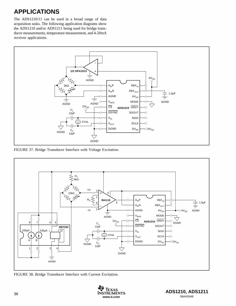
ADS1210, ADS121136SBAS034Bwww.ti.com
FIGURE 37. Bridge Transducer Interface with Voltage Excitation.
FIGURE 38. Bridge Transducer Interface with Current Excitation.
APPLICATIONSThe ADS1210/11 can be used in a broad range of dataacquisition tasks. The following application diagrams showthe ADS1210 and/or ADS1211 being used for bridge trans-ducer measurements, temperature measurement, and 4-20mAreceiver applications.
ADS1210
AINP
AINN
AGND
VBIAS
CS
DSYNC
XIN
XOUT
DGND
REFIN
REFOUT
AVDD
MODE
DRDY
SDOUT
SDIO
SCLK
DVDDC212pF
C112pF
DVDD
AGND
DGND
AGND
AVDD
DVDDDGND
1/2 OPA1013
3kΩ
AGND
XTAL
AGND
1.0µF
ADS1210
AINP
AINN
AGND
VBIAS
CS
DSYNC
XIN
XOUT
DGND
REFIN
REFOUT
AVDD
MODE
DRDY
SDOUT
SDIO
SCLK
DVDDC212pF
C112pF
XTAL
DVDD
DGND
DGND
AGND
DGND
AGND
AVDD
DVDD
INA118
10kΩ1
35
8
2
6RG
+In
–In
R16kΩ
7
A B
O
C
I
REF200
1 2 3 4
8 6 5
100µA 100µA
AGND
1.0µF
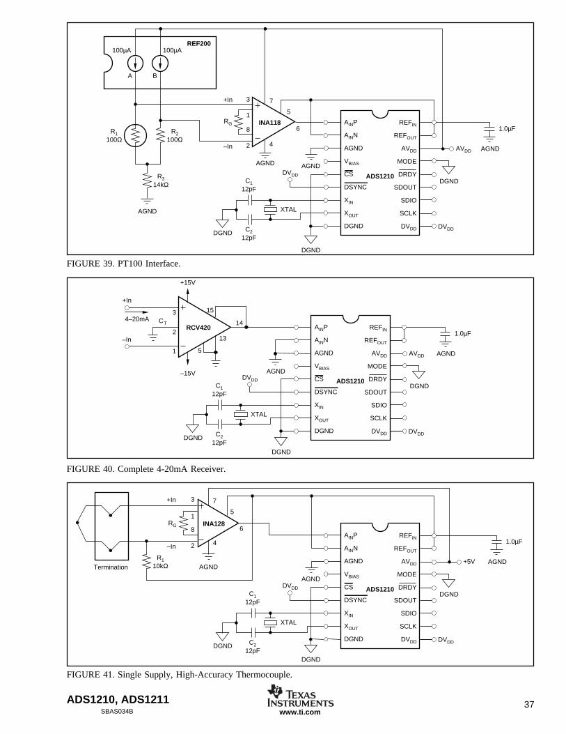
ADS1210, ADS1211 37SBAS034B www.ti.com
FIGURE 39. PT100 Interface.
FIGURE 40. Complete 4-20mA Receiver.
FIGURE 41. Single Supply, High-Accuracy Thermocouple.
ADS1210
AINP
AINN
AGND
VBIAS
CS
DSYNC
XIN
XOUT
DGND
REFIN
REFOUT
AVDD
MODE
DRDY
SDOUT
SDIO
SCLK
DVDDC212pF
C112pF
DVDD
AGND
DGND
DGND
DGND
XTAL
AVDD
DVDD
RCV420
15
+In
3
2–In
1
CT
–15V
14
13
5
+15V
4–20mA
AGND
1.0µF
ADS1210
AINP
AINN
AGND
VBIAS
CS
DSYNC
XIN
XOUT
DGND
REFIN
REFOUT
AVDD
MODE
DRDY
SDOUT
SDIO
SCLK
DVDDC212pF
C112pF
DVDD
AGND
DGND
DGND
DGND
AGND XTAL
AGND
AVDD
DVDD
INA1181
3 7
4
8
2
6
5
RG
+In
–In
A B
REF200100µA 100µA
R314kΩ
R2100Ω
R1100Ω
AGND
1.0µF
ADS1210
AINP
AINN
AGND
VBIAS
CS
DSYNC
XIN
XOUT
DGND
REFIN
REFOUT
AVDD
MODE
DRDY
SDOUT
SDIO
SCLK
DVDDC212pF
C112pF
DVDD
AGND
DGND
DGND
DGND
XTAL
+5V
DVDD
INA128RG
R110kΩ AGND
1
3 7
8
2
6
4
5
+In
–In
TerminationAGND
1.0µF
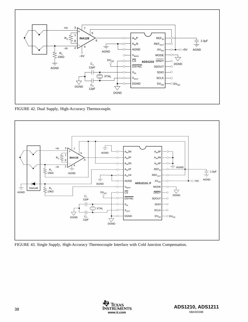
ADS1210, ADS121138SBAS034Bwww.ti.com
C212pF
C112pF
DVDD
DGND
XTAL
+5V
DVDD
AGND
AGND
AGND
DGND
DGND
INA118RG
R110kΩ
R213kΩAGND
1
3 7
8
2
6
4
5
+In
–In
ADS1211U, P
AIN3N
AIN2P
AIN2N
AIN1P
AIN1N
AGND
VBIAS
CS
DSYNC
XIN
XOUT
DGND
AIN3P
AIN4N
AIN4P
REFIN
REFOUT
AVDD
MODE
DRDY
SDOUT
SDIO
SCLK
DVDD
AGND
1N4148
AGND
1.0µF
FIGURE 42. Dual Supply, High-Accuracy Thermocouple.
FIGURE 43. Single Supply, High-Accuracy Thermocouple Interface with Cold Junction Compensation.
ADS1210
AINP
AINN
AGND
VBIAS
CS
DSYNC
XIN
XOUT
DGND
REFIN
REFOUT
AVDD
MODE
DRDY
SDOUT
SDIO
SCLK
DVDDC212pF
C112pF
DVDD
DGND
DGND
DGND
XTAL
+5V
DVDD
AGND
AGND
INA128RG
R110kΩ
1
3 7
8
2
6
4
5
+In
–In
–5V
AGND
1.0µF
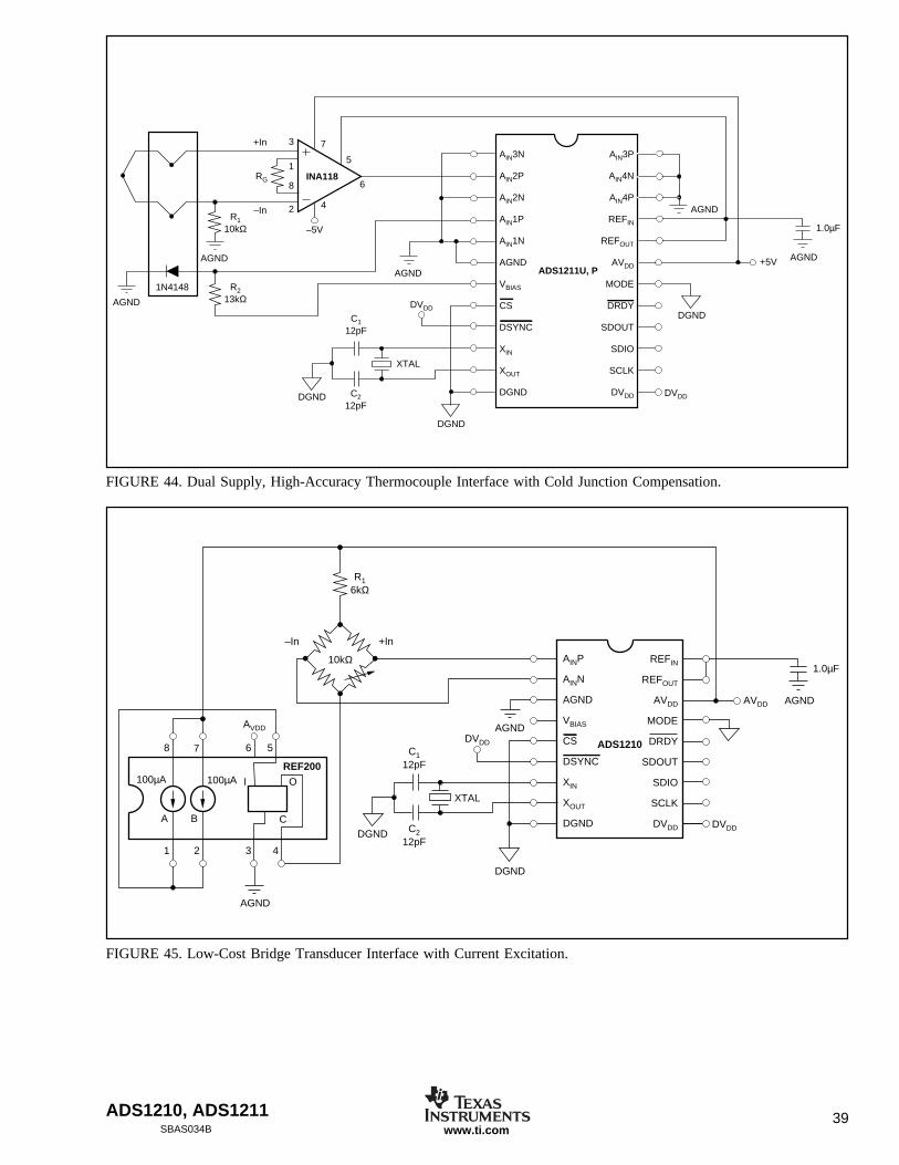
ADS1210, ADS1211 39SBAS034B www.ti.com
C212pF
C112pF
DVDD
DGND
XTAL
–5V
+5V
DVDD
AGND
AGND
DGND
DGND
INA118RG
R110kΩ
R213kΩAGND
1
3 7
8
2
6
4
5
+In
–In
ADS1211U, P
AIN3N
AIN2P
AIN2N
AIN1P
AIN1N
AGND
VBIAS
CS
DSYNC
XIN
XOUT
DGND
AIN3P
AIN4N
AIN4P
REFIN
REFOUT
AVDD
MODE
DRDY
SDOUT
SDIO
SCLK
DVDD
AGND
1N4148
AGND
1.0µF
FIGURE 44. Dual Supply, High-Accuracy Thermocouple Interface with Cold Junction Compensation.
FIGURE 45. Low-Cost Bridge Transducer Interface with Current Excitation.
ADS1210
AINP
AINN
AGND
VBIAS
CS
DSYNC
XIN
XOUT
DGND
REFIN
REFOUT
AVDD
MODE
DRDY
SDOUT
SDIO
SCLK
DVDDC212pF
C112pF
XTAL
DVDD
AGNDAVDD
DGND
DGND
AGND
AVDD
DVDD
10kΩ
–In +In
R16kΩ
7
A B
O
C
I
REF200
1 2 3 4
8 6 5
100µA 100µA
AGND
1.0µF
ADS1210, ADS121140SBAS034Bwww.ti.com
TOPIC INDEX
TOPIC PAGE TOPIC PAGE
ANALOG OPERATION .................................................................17
ANALOG INPUT ....................................................................................... 17
REFERENCE INPUT ................................................................................ 17
REFERENCE OUTPUT ............................................................................ 17
VBIAS ..................................................................................................................................................... 18
DIGITAL OPERATION ..................................................................18
SYSTEM CONFIGURATION .................................................................... 18
Instruction Register (INSR) ................................................................... 19
Command Register (CMR) .................................................................... 19
Data Output Register (DOR) ................................................................. 21
Offset Calibration Register (OCR) ........................................................ 22
Full-Scale Calibration Register (FCR) ................................................... 22
TIMING ..................................................................................................... 22
Synchronizing Multiple Converters ........................................................ 26
SERIAL INTERFACE ............................................................................... 26
Multiple Instructions ............................................................................... 26
Using CS and Continuous Read Mode ................................................ 29
Power-On Conditions for SDIO ............................................................. 29
Master Mode .......................................................................................... 29
Slave Mode ............................................................................................ 29
Making Use of DSYNC ......................................................................... 30
Reset, Power-On Reset, and Brown-Out ............................................. 30
Two-Wire Interface ................................................................................ 30
Three-Wire Interface .............................................................................. 30
Four-Wire Interface ................................................................................ 30
Multi-Wire Interface ............................................................................... 32
I/O Recovery .......................................................................................... 32
Isolation ................................................................................................. 33
Synchronization of Multiple Converters ................................................ 34
LAYOUT ........................................................................................ 35
POWER SUPPLIES ................................................................................. 35
GROUNDING............................................................................................ 35
DECOUPLING .......................................................................................... 35
SYSTEM CONSIDERATIONS ................................................................. 35
APPLICATIONS ............................................................................36
FEATURES ..................................................................................... 1
APPLICATIONS ............................................................................. 1
DESCRIPTION ............................................................................... 1
SPECIFICATIONS .......................................................................... 2
ABSOLUTE MAXIMUM RATINGS ............................................................. 3
ELECTROSTATIC DISCHARGE SENSITIVITY ........................................ 3
PACKAGE INFORMATION ........................................................................ 3
ORDERING INFORMATION ...................................................................... 3
ADS1210 SIMPLIFIED BLOCK DIAGRAM ................................................ 4
ADS1210 PIN CONFIGURATION .............................................................. 4
ADS1210 PIN DEFINITIONS ..................................................................... 4
ADS1211 SIMPLIFIED BLOCK DIAGRAM ................................................ 5
ADS1211P and ADS1211U PIN CONFIGURATION ................................. 5
ADS1211P and ADS1211U PIN DEFINITIONS ........................................ 5
ADS1211E PIN CONFIGURATION ........................................................... 6
ADS1211E PIN DEFINITIONS ................................................................... 6
TYPICAL PERFORMANCE CURVES ........................................... 7
THEORY OF OPERATION ............................................................ 9
DEFINITION OF TERMS ......................................................................... 10
DIGITAL FILTER ...................................................................................... 11
Filter Equation ....................................................................................... 12
Filter Settling .......................................................................................... 12
TURBO MODE ......................................................................................... 12
PROGRAMMABLE GAIN AMPLIFIER ..................................................... 13
SOFTWARE GAIN ................................................................................... 13
CALIBRATION .......................................................................................... 13
Self-Calibration ...................................................................................... 14
System Offset Calibration ..................................................................... 14
System Full-Scale Calibration ............................................................... 14
Pseudo System Calibration ................................................................... 15
Background Calibration ......................................................................... 15
System Calibration Offset and Full-Scale Calibration Limits ................ 16
SLEEP MODE .......................................................................................... 16
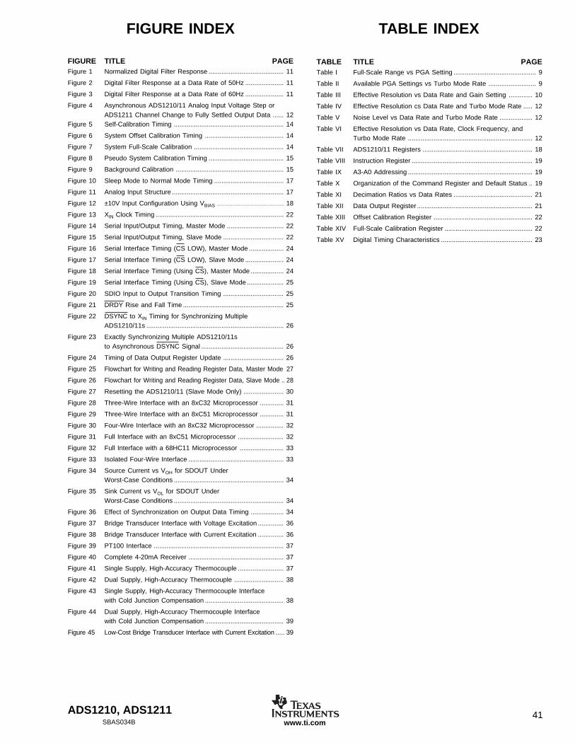
ADS1210, ADS1211 41SBAS034B www.ti.com
FIGURE INDEX TABLE INDEX
FIGURE TITLE PAGEFigure 1 Normalized Digital Filter Response ......................................... 11
Figure 2 Digital Filter Response at a Data Rate of 50Hz ..................... 11
Figure 3 Digital Filter Response at a Data Rate of 60Hz ..................... 11
Figure 4 Asynchronous ADS1210/11 Analog Input Voltage Step orADS1211 Channel Change to Fully Settled Output Data ...... 12
Figure 5 Self-Calibration Timing ............................................................ 14
Figure 6 System Offset Calibration Timing ........................................... 14
Figure 7 System Full-Scale Calibration ................................................. 14
Figure 8 Pseudo System Calibration Timing ......................................... 15
Figure 9 Background Calibration ........................................................... 15
Figure 10 Sleep Mode to Normal Mode Timing ...................................... 17
Figure 11 Analog Input Structure ............................................................. 17
Figure 12 ±10V Input Configuration Using VBIAS .................................................... 18
Figure 13 XIN Clock Timing ...................................................................... 22
Figure 14 Serial Input/Output Timing, Master Mode ............................... 22
Figure 15 Serial Input/Output Timing, Slave Mode ................................. 22
Figure 16 Serial Interface Timing (CS LOW), Master Mode ................... 24
Figure 17 Serial Interface Timing (CS LOW), Slave Mode ..................... 24
Figure 18 Serial Interface Timing (Using CS), Master Mode .................. 24
Figure 19 Serial Interface Timing (Using CS), Slave Mode .................... 25
Figure 20 SDIO Input to Output Transition Timing ................................. 25
Figure 21 DRDY Rise and Fall Time ....................................................... 25
Figure 22 DSYNC to XIN Timing for Synchronizing MultipleADS1210/11s ........................................................................... 26
Figure 23 Exactly Synchronizing Multiple ADS1210/11sto Asynchronous DSYNC Signal ............................................. 26
Figure 24 Timing of Data Output Register Update ................................. 26
Figure 25 Flowchart for Writing and Reading Register Data, Master Mode 27
Figure 26 Flowchart for Writing and Reading Register Data, Slave Mode .. 28
Figure 27 Resetting the ADS1210/11 (Slave Mode Only) ...................... 30
Figure 28 Three-Wire Interface with an 8xC32 Microprocessor ............. 31
Figure 29 Three-Wire Interface with an 8xC51 Microprocessor ............. 31
Figure 30 Four-Wire Interface with an 8xC32 Microprocessor ............... 32
Figure 31 Full Interface with an 8xC51 Microprocessor ......................... 32
Figure 32 Full Interface with a 68HC11 Microprocessor ........................ 33
Figure 33 Isolated Four-Wire Interface .................................................... 33
Figure 34 Source Current vs VOH for SDOUT UnderWorst-Case Conditions ............................................................ 34
Figure 35 Sink Current vs VOL for SDOUT UnderWorst-Case Conditions ............................................................ 34
Figure 36 Effect of Synchronization on Output Data Timing .................. 34
Figure 37 Bridge Transducer Interface with Voltage Excitation .............. 36
Figure 38 Bridge Transducer Interface with Current Excitation .............. 36
Figure 39 PT100 Interface ....................................................................... 37
Figure 40 Complete 4-20mA Receiver .................................................... 37
Figure 41 Single Supply, High-Accuracy Thermocouple ......................... 37
Figure 42 Dual Supply, High-Accuracy Thermocouple ........................... 38
Figure 43 Single Supply, High-Accuracy Thermocouple Interfacewith Cold Junction Compensation ........................................... 38
Figure 44 Dual Supply, High-Accuracy Thermocouple Interfacewith Cold Junction Compensation ........................................... 39
Figure 45 Low-Cost Bridge Transducer Interface with Current Excitation ..... 39
TABLE TITLE PAGETable I Full-Scale Range vs PGA Setting ............................................. 9
Table II Available PGA Settings vs Turbo Mode Rate .......................... 9
Table III Effective Resolution vs Data Rate and Gain Setting ............. 10
Table IV Effective Resolution cs Data Rate and Turbo Mode Rate ..... 12
Table V Noise Level vs Data Rate and Turbo Mode Rate .................. 12
Table VI Effective Resolution vs Data Rate, Clock Frequency, andTurbo Mode Rate .................................................................... 12
Table VII ADS1210/11 Registers ............................................................ 18
Table VIII Instruction Register .................................................................. 19
Table IX A3-A0 Addressing .................................................................... 19
Table X Organization of the Command Register and Default Status .. 19
Table XI Decimation Ratios vs Data Rates ........................................... 21
Table XII Data Output Register ............................................................... 21
Table XIII Offset Calibration Register ...................................................... 22
Table XIV Full-Scale Calibration Register ................................................ 22
Table XV Digital Timing Characteristics .................................................. 23
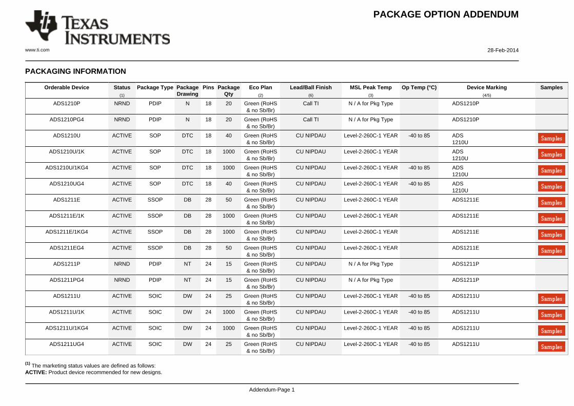
PACKAGE OPTION ADDENDUM
www.ti.com 28-Feb-2014
Addendum-Page 1
PACKAGING INFORMATION
Orderable Device Status(1)
Package Type PackageDrawing
Pins PackageQty
Eco Plan(2)
Lead/Ball Finish(6)
MSL Peak Temp(3)
Op Temp (°C) Device Marking(4/5)
Samples
ADS1210P NRND PDIP N 18 20 Green (RoHS& no Sb/Br)
Call TI N / A for Pkg Type ADS1210P
ADS1210PG4 NRND PDIP N 18 20 Green (RoHS& no Sb/Br)
Call TI N / A for Pkg Type ADS1210P
ADS1210U ACTIVE SOP DTC 18 40 Green (RoHS& no Sb/Br)
CU NIPDAU Level-2-260C-1 YEAR -40 to 85 ADS1210U
ADS1210U/1K ACTIVE SOP DTC 18 1000 Green (RoHS& no Sb/Br)
CU NIPDAU Level-2-260C-1 YEAR ADS1210U
ADS1210U/1KG4 ACTIVE SOP DTC 18 1000 Green (RoHS& no Sb/Br)
CU NIPDAU Level-2-260C-1 YEAR -40 to 85 ADS1210U
ADS1210UG4 ACTIVE SOP DTC 18 40 Green (RoHS& no Sb/Br)
CU NIPDAU Level-2-260C-1 YEAR -40 to 85 ADS1210U
ADS1211E ACTIVE SSOP DB 28 50 Green (RoHS& no Sb/Br)
CU NIPDAU Level-2-260C-1 YEAR ADS1211E
ADS1211E/1K ACTIVE SSOP DB 28 1000 Green (RoHS& no Sb/Br)
CU NIPDAU Level-2-260C-1 YEAR ADS1211E
ADS1211E/1KG4 ACTIVE SSOP DB 28 1000 Green (RoHS& no Sb/Br)
CU NIPDAU Level-2-260C-1 YEAR ADS1211E
ADS1211EG4 ACTIVE SSOP DB 28 50 Green (RoHS& no Sb/Br)
CU NIPDAU Level-2-260C-1 YEAR ADS1211E
ADS1211P NRND PDIP NT 24 15 Green (RoHS& no Sb/Br)
CU NIPDAU N / A for Pkg Type ADS1211P
ADS1211PG4 NRND PDIP NT 24 15 Green (RoHS& no Sb/Br)
CU NIPDAU N / A for Pkg Type ADS1211P
ADS1211U ACTIVE SOIC DW 24 25 Green (RoHS& no Sb/Br)
CU NIPDAU Level-2-260C-1 YEAR -40 to 85 ADS1211U
ADS1211U/1K ACTIVE SOIC DW 24 1000 Green (RoHS& no Sb/Br)
CU NIPDAU Level-2-260C-1 YEAR -40 to 85 ADS1211U
ADS1211U/1KG4 ACTIVE SOIC DW 24 1000 Green (RoHS& no Sb/Br)
CU NIPDAU Level-2-260C-1 YEAR -40 to 85 ADS1211U
ADS1211UG4 ACTIVE SOIC DW 24 25 Green (RoHS& no Sb/Br)
CU NIPDAU Level-2-260C-1 YEAR -40 to 85 ADS1211U
(1) The marketing status values are defined as follows:ACTIVE: Product device recommended for new designs.
PACKAGE OPTION ADDENDUM
www.ti.com 28-Feb-2014
Addendum-Page 2
LIFEBUY: TI has announced that the device will be discontinued, and a lifetime-buy period is in effect.NRND: Not recommended for new designs. Device is in production to support existing customers, but TI does not recommend using this part in a new design.PREVIEW: Device has been announced but is not in production. Samples may or may not be available.OBSOLETE: TI has discontinued the production of the device.
(2) Eco Plan - The planned eco-friendly classification: Pb-Free (RoHS), Pb-Free (RoHS Exempt), or Green (RoHS & no Sb/Br) - please check http://www.ti.com/productcontent for the latest availabilityinformation and additional product content details.TBD: The Pb-Free/Green conversion plan has not been defined.Pb-Free (RoHS): TI's terms "Lead-Free" or "Pb-Free" mean semiconductor products that are compatible with the current RoHS requirements for all 6 substances, including the requirement thatlead not exceed 0.1% by weight in homogeneous materials. Where designed to be soldered at high temperatures, TI Pb-Free products are suitable for use in specified lead-free processes.Pb-Free (RoHS Exempt): This component has a RoHS exemption for either 1) lead-based flip-chip solder bumps used between the die and package, or 2) lead-based die adhesive used betweenthe die and leadframe. The component is otherwise considered Pb-Free (RoHS compatible) as defined above.Green (RoHS & no Sb/Br): TI defines "Green" to mean Pb-Free (RoHS compatible), and free of Bromine (Br) and Antimony (Sb) based flame retardants (Br or Sb do not exceed 0.1% by weightin homogeneous material)
(3) MSL, Peak Temp. - The Moisture Sensitivity Level rating according to the JEDEC industry standard classifications, and peak solder temperature.
(4) There may be additional marking, which relates to the logo, the lot trace code information, or the environmental category on the device.
(5) Multiple Device Markings will be inside parentheses. Only one Device Marking contained in parentheses and separated by a "~" will appear on a device. If a line is indented then it is a continuationof the previous line and the two combined represent the entire Device Marking for that device.
(6) Lead/Ball Finish - Orderable Devices may have multiple material finish options. Finish options are separated by a vertical ruled line. Lead/Ball Finish values may wrap to two lines if the finishvalue exceeds the maximum column width.
Important Information and Disclaimer:The information provided on this page represents TI's knowledge and belief as of the date that it is provided. TI bases its knowledge and belief on informationprovided by third parties, and makes no representation or warranty as to the accuracy of such information. Efforts are underway to better integrate information from third parties. TI has taken andcontinues to take reasonable steps to provide representative and accurate information but may not have conducted destructive testing or chemical analysis on incoming materials and chemicals.TI and TI suppliers consider certain information to be proprietary, and thus CAS numbers and other limited information may not be available for release.
In no event shall TI's liability arising out of such information exceed the total purchase price of the TI part(s) at issue in this document sold by TI to Customer on an annual basis.
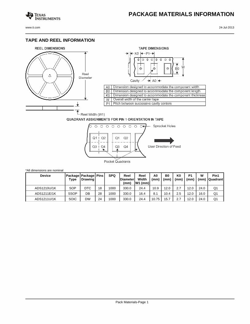
TAPE AND REEL INFORMATION
*All dimensions are nominal
Device PackageType
PackageDrawing
Pins SPQ ReelDiameter
(mm)
ReelWidth
W1 (mm)
A0(mm)
B0(mm)
K0(mm)
P1(mm)
W(mm)
Pin1Quadrant
ADS1210U/1K SOP DTC 18 1000 330.0 24.4 10.9 12.0 2.7 12.0 24.0 Q1
ADS1211E/1K SSOP DB 28 1000 330.0 16.4 8.1 10.4 2.5 12.0 16.0 Q1
ADS1211U/1K SOIC DW 24 1000 330.0 24.4 10.75 15.7 2.7 12.0 24.0 Q1
PACKAGE MATERIALS INFORMATION
www.ti.com 24-Jul-2013
Pack Materials-Page 1

*All dimensions are nominal
Device Package Type Package Drawing Pins SPQ Length (mm) Width (mm) Height (mm)
ADS1210U/1K SOP DTC 18 1000 367.0 367.0 45.0
ADS1211E/1K SSOP DB 28 1000 367.0 367.0 38.0
ADS1211U/1K SOIC DW 24 1000 367.0 367.0 45.0
PACKAGE MATERIALS INFORMATION
www.ti.com 24-Jul-2013
Pack Materials-Page 2
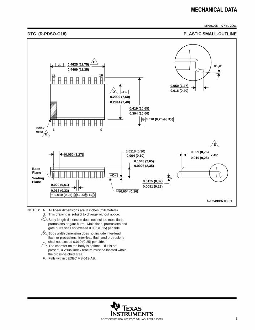
MECHANICAL DATA
MPDS095 – APRIL 2001
1POST OFFICE BOX 655303 • DALLAS, TEXAS 75265
DTC (R-PDSO-G18) PLASTIC SMALL-OUTLINE
4202498/A 03/01
Area1
18 10
9
0.4469 (11,35)
0.4625 (11,75)–A– 0°–8°
0.016 (0,40)0.050 (1,27)
0.2914 (7,40)
0.2992 (7,60)
0.394 (10,00)
0.419 (10,65)
0.010 (0,25) B
0.0091 (0,23)
0.0125 (0,32)
BasePlane
SeatingPlane
0.004 (0,10)0.0118 (0,30)
0.0926 (2,35)0.1043 (2,65)
0.004 (0,10)
0.010 (0,25)
0.029 (0,75)0.050 (1,27)
0.013 (0,33)
0.020 (0,51)
Index
x 45°
M
C
D –B–
M
E
0.010 (0,25) M MC A B S
–C–
E
NOTES: A. All linear dimensions are in inches (millimeters).B. This drawing is subject to change without notice.
C. Body length dimension does not include mold flash,protrusions or gate burrs. Mold flash, protrusions andgate burrs shall not exceed 0.006 (0,15) per side.
D. Body width dimension does not include inter-leadflash or protrusions. Inter-lead flash and protrusionsshall not exceed 0.010 (0,25) per side.
E. The chamfer on the body is optional. If it is notpresent, a visual index feature must be located withinthe cross-hatched area.
F. Falls within JEDEC MS-013-AB.
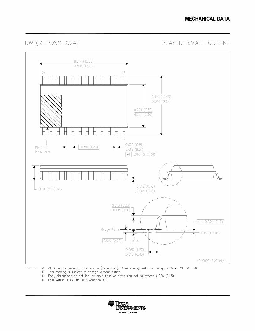
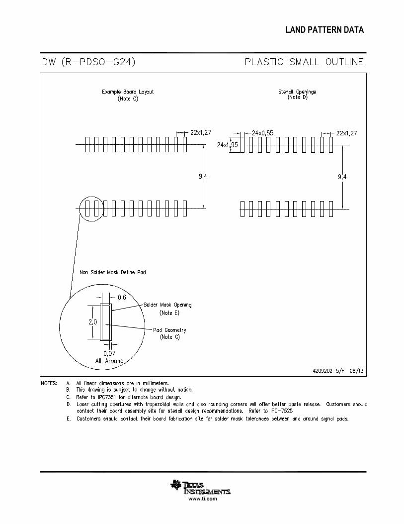
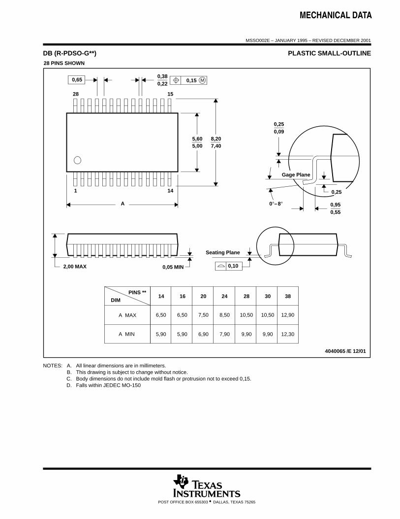
MECHANICAL DATA
MSSO002E – JANUARY 1995 – REVISED DECEMBER 2001
POST OFFICE BOX 655303 • DALLAS, TEXAS 75265
DB (R-PDSO-G**) PLASTIC SMALL-OUTLINE
4040065 /E 12/01
28 PINS SHOWN
Gage Plane
8,207,40
0,550,95
0,25
38
12,90
12,30
28
10,50
24
8,50
Seating Plane
9,907,90
30
10,50
9,90
0,38
5,605,00
15
0,22
14
A
28
1
2016
6,506,50
14
0,05 MIN
5,905,90
DIM
A MAX
A MIN
PINS **
2,00 MAX
6,90
7,50
0,65 M0,15
0°–8°
0,10
0,090,25
NOTES: A. All linear dimensions are in millimeters.B. This drawing is subject to change without notice.C. Body dimensions do not include mold flash or protrusion not to exceed 0,15.D. Falls within JEDEC MO-150

IMPORTANT NOTICETexas Instruments Incorporated and its subsidiaries (TI) reserve the right to make corrections, enhancements, improvements and otherchanges to its semiconductor products and services per JESD46, latest issue, and to discontinue any product or service per JESD48, latestissue. Buyers should obtain the latest relevant information before placing orders and should verify that such information is current andcomplete. All semiconductor products (also referred to herein as “components”) are sold subject to TI’s terms and conditions of salesupplied at the time of order acknowledgment.TI warrants performance of its components to the specifications applicable at the time of sale, in accordance with the warranty in TI’s termsand conditions of sale of semiconductor products. Testing and other quality control techniques are used to the extent TI deems necessaryto support this warranty. Except where mandated by applicable law, testing of all parameters of each component is not necessarilyperformed.TI assumes no liability for applications assistance or the design of Buyers’ products. Buyers are responsible for their products andapplications using TI components. To minimize the risks associated with Buyers’ products and applications, Buyers should provideadequate design and operating safeguards.TI does not warrant or represent that any license, either express or implied, is granted under any patent right, copyright, mask work right, orother intellectual property right relating to any combination, machine, or process in which TI components or services are used. Informationpublished by TI regarding third-party products or services does not constitute a license to use such products or services or a warranty orendorsement thereof. Use of such information may require a license from a third party under the patents or other intellectual property of thethird party, or a license from TI under the patents or other intellectual property of TI.Reproduction of significant portions of TI information in TI data books or data sheets is permissible only if reproduction is without alterationand is accompanied by all associated warranties, conditions, limitations, and notices. TI is not responsible or liable for such altereddocumentation. Information of third parties may be subject to additional restrictions.Resale of TI components or services with statements different from or beyond the parameters stated by TI for that component or servicevoids all express and any implied warranties for the associated TI component or service and is an unfair and deceptive business practice.TI is not responsible or liable for any such statements.Buyer acknowledges and agrees that it is solely responsible for compliance with all legal, regulatory and safety-related requirementsconcerning its products, and any use of TI components in its applications, notwithstanding any applications-related information or supportthat may be provided by TI. Buyer represents and agrees that it has all the necessary expertise to create and implement safeguards whichanticipate dangerous consequences of failures, monitor failures and their consequences, lessen the likelihood of failures that might causeharm and take appropriate remedial actions. Buyer will fully indemnify TI and its representatives against any damages arising out of the useof any TI components in safety-critical applications.In some cases, TI components may be promoted specifically to facilitate safety-related applications. With such components, TI’s goal is tohelp enable customers to design and create their own end-product solutions that meet applicable functional safety standards andrequirements. Nonetheless, such components are subject to these terms.No TI components are authorized for use in FDA Class III (or similar life-critical medical equipment) unless authorized officers of the partieshave executed a special agreement specifically governing such use.Only those TI components which TI has specifically designated as military grade or “enhanced plastic” are designed and intended for use inmilitary/aerospace applications or environments. Buyer acknowledges and agrees that any military or aerospace use of TI componentswhich have not been so designated is solely at the Buyer's risk, and that Buyer is solely responsible for compliance with all legal andregulatory requirements in connection with such use.TI has specifically designated certain components as meeting ISO/TS16949 requirements, mainly for automotive use. In any case of use ofnon-designated products, TI will not be responsible for any failure to meet ISO/TS16949.Products ApplicationsAudio www.ti.com/audio Automotive and Transportation www.ti.com/automotiveAmplifiers amplifier.ti.com Communications and Telecom www.ti.com/communicationsData Converters dataconverter.ti.com Computers and Peripherals www.ti.com/computersDLP® Products www.dlp.com Consumer Electronics www.ti.com/consumer-appsDSP dsp.ti.com Energy and Lighting www.ti.com/energyClocks and Timers www.ti.com/clocks Industrial www.ti.com/industrialInterface interface.ti.com Medical www.ti.com/medicalLogic logic.ti.com Security www.ti.com/securityPower Mgmt power.ti.com Space, Avionics and Defense www.ti.com/space-avionics-defenseMicrocontrollers microcontroller.ti.com Video and Imaging www.ti.com/videoRFID www.ti-rfid.comOMAP Applications Processors www.ti.com/omap TI E2E Community e2e.ti.comWireless Connectivity www.ti.com/wirelessconnectivity
Mailing Address: Texas Instruments, Post Office Box 655303, Dallas, Texas 75265Copyright © 2014, Texas Instruments Incorporated