Embed Size (px)
Citation preview

2130 IEEE JOURNAL OF SOLID-STATE CIRCUITS, VOL. 45, NO. 10, OCTOBER 2010
Circuit Design and Modeling Techniques forEnhancing the Clock-Data Compensation Effect
Under Resonant Supply NoiseDong Jiao, Jie Gu, Member, IEEE, and Chris H. Kim, Member, IEEE
Abstract—Recent publications have shown that clock jitter canimprove timing margin through the compensation effect betweenthe clock cycle and the datapath delay under the influence of res-onant supply noise. This paper presents a comprehensive study ofthis beneficial clock-data compensation effect including an anal-ysis of its dependency on various design parameters and a newphase-shifted clock buffer design that can enhance the effect. Mea-surement result from a 1.2 V, 65 nm test chip shows an 8–27% in-crease in the maximum operating frequency while saving 85% ofthe clock buffer area compared to prior art. An accurate timingmodel is derived to estimate the beneficial jitter effect.
Index Terms—Clock-data compensation, clock distribution, res-onant noise, supply noise.
I. INTRODUCTION
P OWER supply noise is considered to be one of the majorperformance limiting factors in scaled technologies [1].
Traditionally, passive decoupling techniques based on on-chipdecoupling capacitors or damping resistors were used to reducethe supply network impedance [2]–[4]. Several circuit tech-niques have been proposed to alleviate the supply noise impacton circuit performance by minimizing clock jitter [5]–[11].Supply noise in the 100 MHz to 300 MHz resonant frequencyband has been shown as the dominant noise component ina typical high performance microprocessor [12]–[14]. Fig. 1shows the measured supply network impedance of an Intel Ne-halem microprocessor which exhibits a large impedance peakat around 150 MHz [15]. Resonant supply noise is caused bythe LC tank formed between the package/bonding inductanceand the die capacitance and thus affects the entire chip. This socalled “first droop noise” can be excited by a sudden currentspike caused by a clock edge or a processor wakeup operation[16], [17]. Due to its large magnitude, resonant noise consti-tutes the worst-case supply noise scenario which has triggered
Manuscript received November 22, 2009; revised May 09, 2010; acceptedJuly 15, 2010. Date of current version September 24, 2010. This paper was ap-proved by Associate Editor Stephan Rusu. This work was supported in part bythe Semiconductor Research Corporation under award 2008-HJ-1804.
D. Jiao and C. H. Kim are with the Department of Electrical and ComputerEngineering, University of Minnesota, Minneapolis, MN 55455 USA (e-mail:[email protected]).
J. Gu is with the MaxLinear Incorporated, Carlsbad, CA 92011 USA.Color versions of one or more of the figures in this paper are available online
at http://ieeexplore.ieee.org.Digital Object Identifier 10.1109/JSSC.2010.2063931
Fig. 1. Measured supply network impedance response of Intel’s Nehalemmicroprocessor [15].
a flurry of research activities in the circuit design community[3], [14], [18].
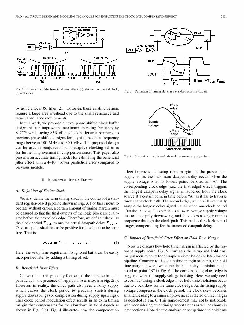
Recent papers have revealed an intriguing timing compensa-tion effect between the clock cycle and the datapath delay inthe presence of resonant supply noise [16], [17], [19]. This phe-nomenon, which we will refer to as the “beneficial jitter” effect,is illustrated in Fig. 2. A simple pipeline circuit consisting of aphase-locked loop (PLL), a clock path and a datapath is shown.In traditional analysis, the clock period is assumed to be con-stant while only the datapath delay is assumed to change underthe influence of supply noise. Fig. 2(b) illustrates example wave-forms based on the traditional analysis showing several sam-pling failures during the event of a supply voltage undershoot.In reality, however, the clock path delay is also modulated bythe supply noise and therefore stretches the clock period duringsupply downswings. As a result, the clock path delay and data-path delay compensate for each other which alleviates the timingmargin. Fig. 2(c) shows example waveforms for this scenario inwhich the output is always sampled correctly by the stretchedclock cycle.
Adaptive clocking schemes utilizing this principle have beenemployed in Intel Nehalem processors [15], [20]. There, a PLL-based clock generator is designed to track the supply noise sothat the clock period stretching effect is maximized. An alter-native way to enhance the beneficial jitter effect is shifting thephase of the supply noise seen by the clock path [16], [17], [19],for example by using an RC filtered supply voltage for the entireclock path. A similar approach has been used in Intel Pentium4processors where the supply noise of the clock buffer is reduced
0018-9200/$26.00 © 2010 IEEE
JIAO et al.: CIRCUIT DESIGN AND MODELING TECHNIQUES FOR ENHANCING THE CLOCK-DATA COMPENSATION EFFECT 2131
Fig. 2. Illustration of the beneficial jitter effect. (a); (b) constant-period clock;(c) real clock.
by using a local RC filter [21]. However, these existing designsrequire a large area overhead due to the small resistance andlarge capacitance requirements.
In this work, we propose a novel phase-shifted clock bufferdesign that can improve the maximum operating frequency by8–27% while saving 85% of the clock buffer area compared toprevious phase-shifted designs for a typical resonant frequencyrange between 100 MHz and 300 MHz. The proposed designcan be used in conjunction with adaptive clocking schemesfor further improvement in chip performance. This paper alsopresents an accurate timing model for estimating the beneficialjitter effect with a 4–10 lower prediction error compared toprevious models.
II. BENEFICIAL JITTER EFFECT
A. Definition of Timing Slack
We first define the term timing slack in the context of a stan-dard register-based pipeline shown in Fig. 3. For this circuit tooperate without errors, a certain amount of timing margin mustbe ensured so that the final outputs of the logic block are evalu-ated before the next clock edge. Therefore, we define “slack” asthe clock period minus the actual datapath delay .Obviously, the slack has to be positive for the circuit to be errorfree. That is:
(1)
Here, the setup time requirement is ignored but it can be easilyincorporated later by adding a timing offset.
B. Beneficial Jitter Effect
Conventional analysis only focuses on the increase in data-path delay in the presence of supply noise as shown in Fig. 2(b).However, in reality, the clock path also sees a noisy supplywhich causes the clock period to gradually stretch duringsupply downswings (or compression during supply upswings).This clock period modulation effect results in an extra timingmargin that compensates for the slowdown in the datapath asshown in Fig. 2(c). Fig. 4 illustrates how the compensation
Fig. 3. Definition of timing slack in a standard pipeline circuit.
Fig. 4. Setup time margin analysis under resonant supply noise.
effect improves the setup time margin. In the presence ofsupply noise, the maximum datapath delay occurs when thesupply voltage is at its lowest point, denoted as “A”. Thecorresponding clock edge (i.e., the first edge) which triggersthe longest datapath delay signal is launched from the clocksource at a certain point in time before “A” as it has to traversethrough the clock path. The second edge, which will eventuallysample the longest delay signal, is launched one clock periodafter the 1st edge. It experiences a lower average supply voltagedue to the supply downswing, and thus takes a longer time topropagate through the clock path. This makes the clock periodlonger, compensating for the increased datapath delay.
C. Impact of Beneficial Jitter Effect on Hold Time Margin
Now we discuss how hold time margin is affected by the res-onant supply noise. Fig. 5 illustrates the setup and hold timemargin requirements for a simple register-based (or latch-based)pipeline. Contrary to the setup time margin scenario, the holdtime margin is worst when the datapath delay is minimum, de-noted as point “B” in Fig. 6. The corresponding clock edge istriggered when the supply voltage is rising. Here, we only needto consider a single clock edge since hold time violations occurdue to clock skew for the same clock edge. As the rising supplyvoltage compresses the clock period, the clock skew becomessmaller, leading to a minor improvement in the hold time marginas depicted in Fig. 6. This improvement may not be noticeablewhen considering other timing uncertainties as will be shown inlater sections. Note that the analysis on setup time and hold time
2132 IEEE JOURNAL OF SOLID-STATE CIRCUITS, VOL. 45, NO. 10, OCTOBER 2010
Fig. 5. Illustration of setup and hold time margin in a register-based (or latch-based) pipeline.
Fig. 6. Hold time margin analysis under resonant supply noise.
margins is applicable to both register-based and latch-based de-signs.
III. MODELING OF BENEFICIAL JITTER EFFECT
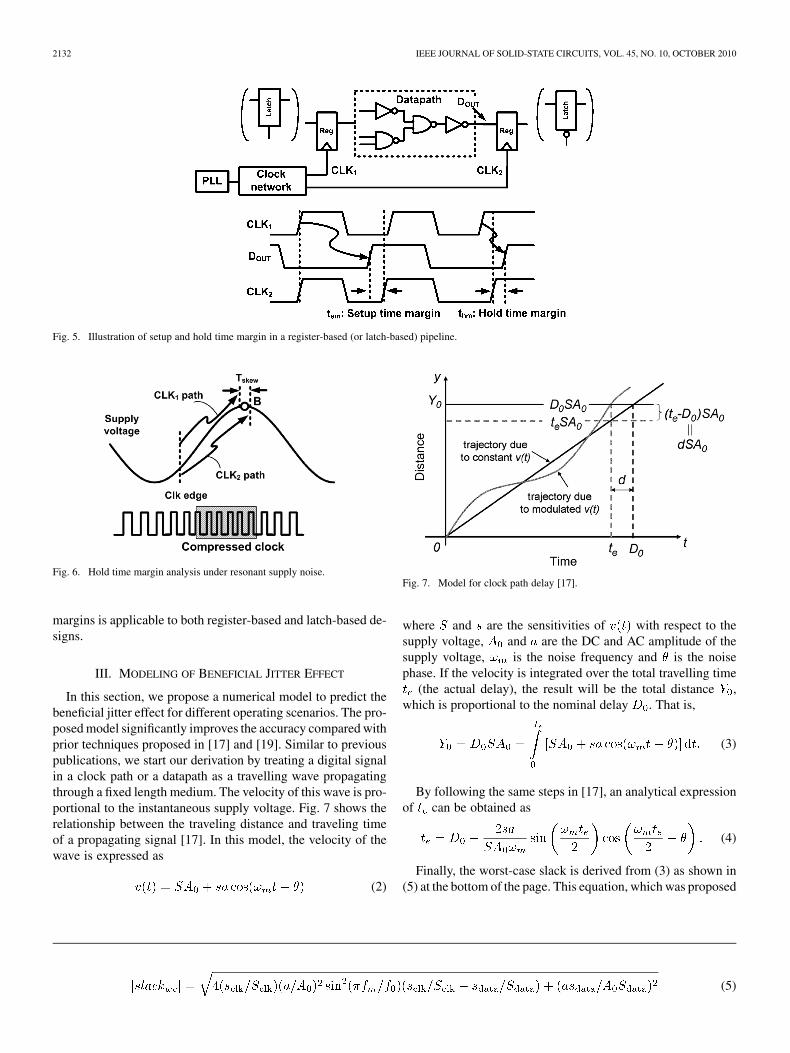
In this section, we propose a numerical model to predict thebeneficial jitter effect for different operating scenarios. The pro-posed model significantly improves the accuracy compared withprior techniques proposed in [17] and [19]. Similar to previouspublications, we start our derivation by treating a digital signalin a clock path or a datapath as a travelling wave propagatingthrough a fixed length medium. The velocity of this wave is pro-portional to the instantaneous supply voltage. Fig. 7 shows therelationship between the traveling distance and traveling timeof a propagating signal [17]. In this model, the velocity of thewave is expressed as
(2)
Fig. 7. Model for clock path delay [17].
where and are the sensitivities of with respect to thesupply voltage, and are the DC and AC amplitude of thesupply voltage, is the noise frequency and is the noisephase. If the velocity is integrated over the total travelling time
(the actual delay), the result will be the total distance ,which is proportional to the nominal delay . That is,
(3)
By following the same steps in [17], an analytical expressionof can be obtained as
(4)
Finally, the worst-case slack is derived from (3) as shown in(5) at the bottom of the page. This equation, which was proposed
(5)
JIAO et al.: CIRCUIT DESIGN AND MODELING TECHNIQUES FOR ENHANCING THE CLOCK-DATA COMPENSATION EFFECT 2133
in [17], predicts a timing improvement only when the delay sen-sitivity of the clock path is less than that of the datapath. How-ever, detailed HSPICE simulation reveals (see Fig. 12) a signif-icant improvement in the worst-case setup time margin (7% ofthe clock period) even when the clock path and the datapath havethe same delay sensitivities. This fact suggests that an improvedmodel is needed to aid designers in better understanding the im-pact of the beneficial jitter effect. In this work, we derive a moreaccurate timing model by using numerical methods to solve (3)rather than resorting to unjustified approximations. Results pre-sented later in this section will show that accurately solving (3)is the most important step in deriving a timing model that is re-liable under various operating conditions.
We will use the standard register-based pipeline circuitshown in Fig. 5 to describe the flow for deriving the setuptiming margin. Suppose the first clock edge launched fromthe clock generation block at time takes to arriveat the register. The input data of the first register starts topropagate through the datapath at time and takes toreach the input of the second register. Now assume the secondclock edge is launched at time and takes topropagate through the clock path. Then, the setup time margincan be calculated as
(6)
This procedure is repeated numerically by sweeping from 0 toand the minimum value becomes the worst-case setup time
margin. For modeling the hold time margin, is set to 0 andtwo different nominal clock path delays are used whensolving for and , indicating that we are considering theclock skew for the same clock edge propagating through twodifferent clock paths.
IV. INTRINSIC BENEFICIAL JITTER EFFECT
In this section, we verify the beneficial jitter effect in an in-dustrial 1.2 V, 65 nm process and analyze its dependency onseveral design parameters. The test circuit is similar to the oneshown in Fig. 3 comprising a 1.9 GHz clock source, an 18-stageinverter chain datapath and an 11-stage clock buffer chain witha nominal delay of 1.0 ns. The delay sensitivities of the clockpath and the datapath with respect to supply noise (i.e., and
) were both set to be 2. Here, we define delay sensitivity asthe percentage increase in the path delay normalized to the per-centage decrease in the supply voltage at a 10% supply noisecondition. That is, a delay sensitivity of 2 means that the delayof a certain path increases by 20% for a 10% decrease in thesupply voltage.
A. Intrinsic Beneficial Jitter Effect
Timing slacks for different clock launching times are shownin Fig. 8 for a 200 MHz resonant supply noise. The x axis showsthe time when a clock edge leaves the clock source and the y axisshows the corresponding timing slack. The dark line representsthe timing slack based on the conventional analysis which onlyconsiders the change in the datapath delay while the gray lineconsiders the change in the clock period as well. An 11 ps (or2.1% of the clock cycle) improvement in the worst-case slackdue to the beneficial jitter effect is observed.
Fig. 8. Slack versus clock launching time under resonant supply noise.
Fig. 9. Dependency of worst-case slack on clock path delay.
B. Factors Affecting the Intrinsic Beneficial Jitter Effect
Clock Path Delay: Fig. 9 shows the dependency of the worst-case slack on the clock path delay simulated by changing thenumber of clock buffer stages. For extremely long or short clockpath delays, the slack considering the beneficial jitter effect (i.e.,noisy clock supply) approaches the conventional analysis case(i.e., clean clock supply). This is because a very short clockpath makes the clock period modulation effect weaker and con-versely, a very long clock path makes each clock edge see asimilar average supply voltage.
Delay Sensitivity to Supply Noise: Fig. 10 shows the sim-ulated worst-case slack when the datapath delay sensitivity isfixed at 2 and the clock path delay sensitivity is varied from 0 to2.4 through the adjustment of the interconnect load, the numberof clock buffer stages, and the supply noise amplitude seen bythe clock path. The optimal timing compensation effect occurswhen the clock path delay sensitivity is around 1.2. A clock pathdelay sensitivity lower than the optimal point makes the clockperiod less sensitive to the supply noise making the beneficialjitter effect weaker. On the other hand, a higher sensitivity even-tually leads to a worse timing slack due to the excessively com-pressed clock periods during supply upswings.
Supply Noise Frequency: The worst-case slack for supplynoise frequencies from 50 MHz to 1.6 GHz are shown in Fig. 11.At extremely low frequencies, the worst-case slack converges to
2134 IEEE JOURNAL OF SOLID-STATE CIRCUITS, VOL. 45, NO. 10, OCTOBER 2010
Fig. 10. Dependency of worst-case slack on clock path delay sensitivity.
Fig. 11. Dependency of worst-case slack on supply noise frequency.
the clean clock case since two consecutive clock edges see al-most the same supply voltage. When the resonant frequency ishigh, the noisy clock supply case again converges to the cleansupply case. This is because of the negligible difference in thesupply voltages seen by two consecutive clock edges due to theaveraging effect.
C. Modeling of Intrinsic Beneficial Jitter Effect
The methodology described in Section III for modeling thebeneficial jitter effect was verified with HSPICE. The clockfrequency and the maximum clock skew were assumed to be1.9 GHz and 20 ps, respectively [22]. A resonant noise with afrequency of 200 MHz and an amplitude of was usedfor the simulations.
In the first test, setup and hold time margins were examinedfor different clock path delays. The results in Fig. 12 show a45 ps change in the setup time margin and the detailed behavioris precisely captured by the proposed model. When comparedwith previous models, the maximum estimation error is im-proved from 26 ps to only 3 ps. Moreover, our proposed modelalso closely matches the simulation results for hold time marginas shown in Fig. 13. The maximum error is less than 1 ps for all
Fig. 12. Dependency of setup time margin on clock path delay.
Fig. 13. Dependency of hold time margin on clock path delay.
TABLE IMAXIMUM MODELING ERROR FOR DIFFERENT CLOCK PATH DELAYS
(� � ��� GHz, � � ��� MHz, � � �, � � �)
clock path delays used in the simulations. A latch-based pipelinecircuit was also simulated and the results are summarized inTable I.
We also tested the accuracy of the model for different supplynoise frequencies. As shown in Fig. 14, the setup time marginis improved due to the beneficial jitter effect for a typical reso-nant frequency range of 100 MHz to 300 MHz. Similar to theprevious test, both setup and hold time margins were simulatedfor register-based and latch-based pipeline circuits and the re-sults are summarized in Table II. A significant improvement inthe modeling accuracy is achieved.
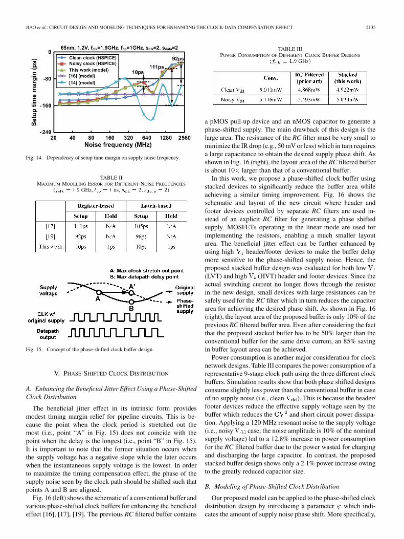
JIAO et al.: CIRCUIT DESIGN AND MODELING TECHNIQUES FOR ENHANCING THE CLOCK-DATA COMPENSATION EFFECT 2135
Fig. 14. Dependency of setup time margin on supply noise frequency.
TABLE IIMAXIMUM MODELING ERROR FOR DIFFERENT NOISE FREQUENCIES
(� � ��� GHz, � � � ns, � � �, � � �)
Fig. 15. Concept of the phase-shifted clock buffer design.
V. PHASE-SHIFTED CLOCK DISTRIBUTION
A. Enhancing the Beneficial Jitter Effect Using a Phase-ShiftedClock Distribution
The beneficial jitter effect in its intrinsic form providesmodest timing margin relief for pipeline circuits. This is be-cause the point when the clock period is stretched out themost (i.e., point “A” in Fig. 15) does not coincide with thepoint when the delay is the longest (i.e., point “B” in Fig. 15).It is important to note that the former situation occurs whenthe supply voltage has a negative slope while the later occurswhen the instantaneous supply voltage is the lowest. In orderto maximize the timing compensation effect, the phase of thesupply noise seen by the clock path should be shifted such thatpoints A and B are aligned.
Fig. 16 (left) shows the schematic of a conventional buffer andvarious phase-shifted clock buffers for enhancing the beneficialeffect [16], [17], [19]. The previous RC filtered buffer contains
TABLE IIIPOWER CONSUMPTION OF DIFFERENT CLOCK BUFFER DESIGNS
�� � ��� GHz�
a pMOS pull-up device and an nMOS capacitor to generate aphase-shifted supply. The main drawback of this design is thelarge area. The resistance of the RC filter must be very small tominimize the IR drop (e.g., 50 mV or less) which in turn requiresa large capacitance to obtain the desired supply phase shift. Asshown in Fig. 16 (right), the layout area of the RC filtered bufferis about 10 larger than that of a conventional buffer.
In this work, we propose a phase-shifted clock buffer usingstacked devices to significantly reduce the buffer area whileachieving a similar timing improvement. Fig. 16 shows theschematic and layout of the new circuit where header andfooter devices controlled by separate RC filters are used in-stead of an explicit RC filter for generating a phase shiftedsupply. MOSFETs operating in the linear mode are used forimplementing the resistors, enabling a much smaller layoutarea. The beneficial jitter effect can be further enhanced byusing high header/footer devices to make the buffer delaymore sensitive to the phase-shifted supply noise. Hence, theproposed stacked buffer design was evaluated for both low(LVT) and high (HVT) header and footer devices. Since theactual switching current no longer flows through the resistorin the new design, small devices with large resistances can besafely used for the RC filter which in turn reduces the capacitorarea for achieving the desired phase shift. As shown in Fig. 16(right), the layout area of the proposed buffer is only 10% of theprevious RC filtered buffer area. Even after considering the factthat the proposed stacked buffer has to be 50% larger than theconventional buffer for the same drive current, an 85% savingin buffer layout area can be achieved.
Power consumption is another major consideration for clocknetwork designs. Table III compares the power consumption of arepresentative 9-stage clock path using the three different clockbuffers. Simulation results show that both phase shifted designsconsume slightly less power than the conventional buffer in caseof no supply noise (i.e., clean ). This is because the header/footer devices reduce the effective supply voltage seen by thebuffer which reduces the and short circuit power dissipa-tion. Applying a 120 MHz resonant noise to the supply voltage(i.e., noisy case, the noise amplitude is 10% of the nominalsupply voltage) led to a 12.8% increase in power consumptionfor the RC filtered buffer due to the power wasted for chargingand discharging the large capacitor. In contrast, the proposedstacked buffer design shows only a 2.1% power increase owingto the greatly reduced capacitor size.
B. Modeling of Phase-Shifted Clock Distribution
Our proposed model can be applied to the phase-shifted clockdistribution design by introducing a parameter which indi-cates the amount of supply noise phase shift. More specifically,
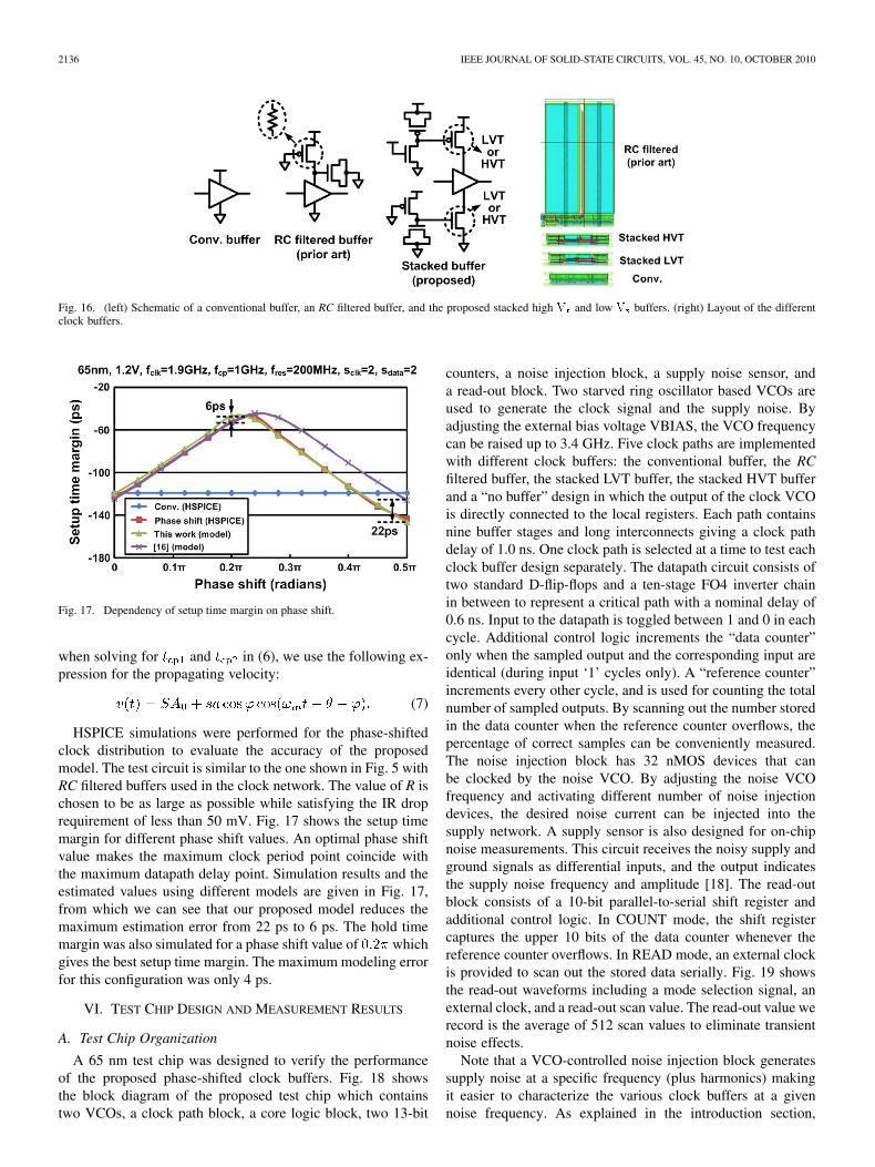
2136 IEEE JOURNAL OF SOLID-STATE CIRCUITS, VOL. 45, NO. 10, OCTOBER 2010
Fig. 16. (left) Schematic of a conventional buffer, an RC filtered buffer, and the proposed stacked high � and low � buffers. (right) Layout of the differentclock buffers.
Fig. 17. Dependency of setup time margin on phase shift.
when solving for and in (6), we use the following ex-pression for the propagating velocity:
(7)
HSPICE simulations were performed for the phase-shiftedclock distribution to evaluate the accuracy of the proposedmodel. The test circuit is similar to the one shown in Fig. 5 withRC filtered buffers used in the clock network. The value of R ischosen to be as large as possible while satisfying the IR droprequirement of less than 50 mV. Fig. 17 shows the setup timemargin for different phase shift values. An optimal phase shiftvalue makes the maximum clock period point coincide withthe maximum datapath delay point. Simulation results and theestimated values using different models are given in Fig. 17,from which we can see that our proposed model reduces themaximum estimation error from 22 ps to 6 ps. The hold timemargin was also simulated for a phase shift value of whichgives the best setup time margin. The maximum modeling errorfor this configuration was only 4 ps.
VI. TEST CHIP DESIGN AND MEASUREMENT RESULTS
A. Test Chip Organization
A 65 nm test chip was designed to verify the performanceof the proposed phase-shifted clock buffers. Fig. 18 showsthe block diagram of the proposed test chip which containstwo VCOs, a clock path block, a core logic block, two 13-bit
counters, a noise injection block, a supply noise sensor, anda read-out block. Two starved ring oscillator based VCOs areused to generate the clock signal and the supply noise. Byadjusting the external bias voltage VBIAS, the VCO frequencycan be raised up to 3.4 GHz. Five clock paths are implementedwith different clock buffers: the conventional buffer, the RCfiltered buffer, the stacked LVT buffer, the stacked HVT bufferand a “no buffer” design in which the output of the clock VCOis directly connected to the local registers. Each path containsnine buffer stages and long interconnects giving a clock pathdelay of 1.0 ns. One clock path is selected at a time to test eachclock buffer design separately. The datapath circuit consists oftwo standard D-flip-flops and a ten-stage FO4 inverter chainin between to represent a critical path with a nominal delay of0.6 ns. Input to the datapath is toggled between 1 and 0 in eachcycle. Additional control logic increments the “data counter”only when the sampled output and the corresponding input areidentical (during input ‘1’ cycles only). A “reference counter”increments every other cycle, and is used for counting the totalnumber of sampled outputs. By scanning out the number storedin the data counter when the reference counter overflows, thepercentage of correct samples can be conveniently measured.The noise injection block has 32 nMOS devices that canbe clocked by the noise VCO. By adjusting the noise VCOfrequency and activating different number of noise injectiondevices, the desired noise current can be injected into thesupply network. A supply sensor is also designed for on-chipnoise measurements. This circuit receives the noisy supply andground signals as differential inputs, and the output indicatesthe supply noise frequency and amplitude [18]. The read-outblock consists of a 10-bit parallel-to-serial shift register andadditional control logic. In COUNT mode, the shift registercaptures the upper 10 bits of the data counter whenever thereference counter overflows. In READ mode, an external clockis provided to scan out the stored data serially. Fig. 19 showsthe read-out waveforms including a mode selection signal, anexternal clock, and a read-out scan value. The read-out value werecord is the average of 512 scan values to eliminate transientnoise effects.
Note that a VCO-controlled noise injection block generatessupply noise at a specific frequency (plus harmonics) makingit easier to characterize the various clock buffers at a givennoise frequency. As explained in the introduction section,
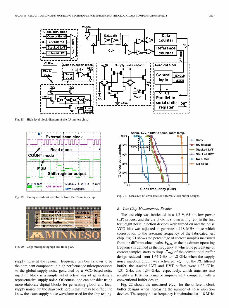
JIAO et al.: CIRCUIT DESIGN AND MODELING TECHNIQUES FOR ENHANCING THE CLOCK-DATA COMPENSATION EFFECT 2137
Fig. 18. High level block diagram of the 65 nm test chip.
Fig. 19. Example read-out waveforms from the 65 nm test chip.
Fig. 20. Chip microphotograph and floor plan.
supply noise at the resonant frequency has been shown to bethe dominant component in high performance microprocessorsso the global supply noise generated by a VCO-based noiseinjection block is a simple yet effective way of generating arepresentative supply noise. Of course, one can consider usingmore elaborate digital blocks for generating global and localsupply noises but the drawback here is that it may be difficult toknow the exact supply noise waveform used for the chip testing.
Fig. 21. Measured bit error rate for different clock buffer designs.
B. Test Chip Measurement Results
The test chip was fabricated in a 1.2 V, 65 nm low power(LP) process and the die photo is shown in Fig. 20. In the firsttest, eight noise injection devices were turned on and the noiseVCO bias was adjusted to generate a 118 MHz noise whichcorresponds to the resonant frequency of the fabricated testchip. Fig. 21 shows the percentage of correct samples measuredfrom the different clock paths. or the maximum operatingfrequency is defined as the frequency at which the percentage ofcorrect samples starts to drop. of the conventional bufferdesign reduced from 1.64 GHz to 1.2 GHz when the supplynoise injection circuit was activated. of the RC filteredbuffer, the stacked LVT and HVT buffers were 1.33 GHz,1.31 GHz, and 1.34 GHz, respectively, which translate intoroughly a 10% performance improvement compared with aconventional buffer design.
Fig. 22 shows the measured for the different clockbuffer designs when increasing the number of noise injectiondevices. The supply noise frequency is maintained at 118 MHz.
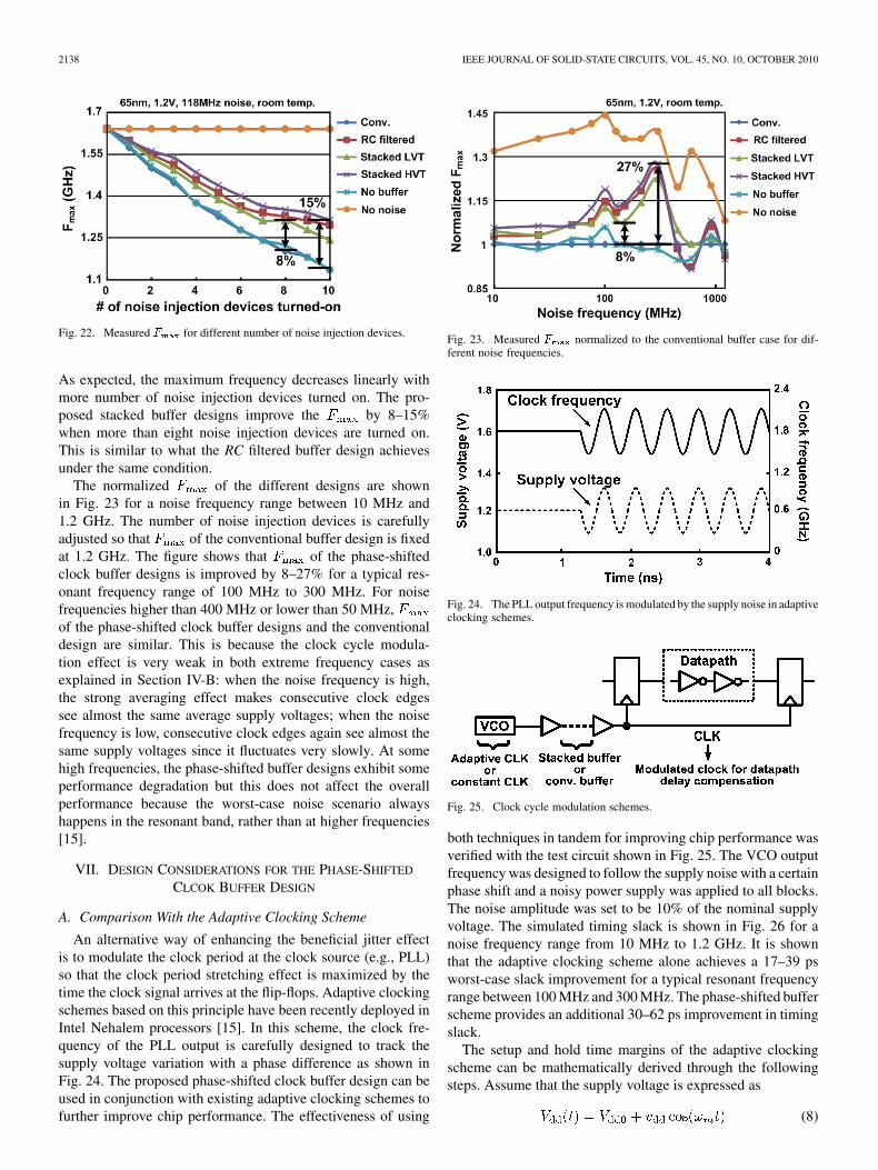
2138 IEEE JOURNAL OF SOLID-STATE CIRCUITS, VOL. 45, NO. 10, OCTOBER 2010
Fig. 22. Measured � for different number of noise injection devices.
As expected, the maximum frequency decreases linearly withmore number of noise injection devices turned on. The pro-posed stacked buffer designs improve the by 8–15%when more than eight noise injection devices are turned on.This is similar to what the RC filtered buffer design achievesunder the same condition.
The normalized of the different designs are shownin Fig. 23 for a noise frequency range between 10 MHz and1.2 GHz. The number of noise injection devices is carefullyadjusted so that of the conventional buffer design is fixedat 1.2 GHz. The figure shows that of the phase-shiftedclock buffer designs is improved by 8–27% for a typical res-onant frequency range of 100 MHz to 300 MHz. For noisefrequencies higher than 400 MHz or lower than 50 MHz,of the phase-shifted clock buffer designs and the conventionaldesign are similar. This is because the clock cycle modula-tion effect is very weak in both extreme frequency cases asexplained in Section IV-B: when the noise frequency is high,the strong averaging effect makes consecutive clock edgessee almost the same average supply voltages; when the noisefrequency is low, consecutive clock edges again see almost thesame supply voltages since it fluctuates very slowly. At somehigh frequencies, the phase-shifted buffer designs exhibit someperformance degradation but this does not affect the overallperformance because the worst-case noise scenario alwayshappens in the resonant band, rather than at higher frequencies[15].
VII. DESIGN CONSIDERATIONS FOR THE PHASE-SHIFTED
CLCOK BUFFER DESIGN
A. Comparison With the Adaptive Clocking Scheme
An alternative way of enhancing the beneficial jitter effectis to modulate the clock period at the clock source (e.g., PLL)so that the clock period stretching effect is maximized by thetime the clock signal arrives at the flip-flops. Adaptive clockingschemes based on this principle have been recently deployed inIntel Nehalem processors [15]. In this scheme, the clock fre-quency of the PLL output is carefully designed to track thesupply voltage variation with a phase difference as shown inFig. 24. The proposed phase-shifted clock buffer design can beused in conjunction with existing adaptive clocking schemes tofurther improve chip performance. The effectiveness of using
Fig. 23. Measured � normalized to the conventional buffer case for dif-ferent noise frequencies.
Fig. 24. The PLL output frequency is modulated by the supply noise in adaptiveclocking schemes.
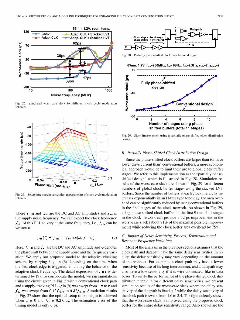
Fig. 25. Clock cycle modulation schemes.
both techniques in tandem for improving chip performance wasverified with the test circuit shown in Fig. 25. The VCO outputfrequency was designed to follow the supply noise with a certainphase shift and a noisy power supply was applied to all blocks.The noise amplitude was set to be 10% of the nominal supplyvoltage. The simulated timing slack is shown in Fig. 26 for anoise frequency range from 10 MHz to 1.2 GHz. It is shownthat the adaptive clocking scheme alone achieves a 17–39 psworst-case slack improvement for a typical resonant frequencyrange between 100 MHz and 300 MHz. The phase-shifted bufferscheme provides an additional 30–62 ps improvement in timingslack.
The setup and hold time margins of the adaptive clockingscheme can be mathematically derived through the followingsteps. Assume that the supply voltage is expressed as
(8)
JIAO et al.: CIRCUIT DESIGN AND MODELING TECHNIQUES FOR ENHANCING THE CLOCK-DATA COMPENSATION EFFECT 2139
Fig. 26. Simulated worst-case slack for different clock cycle modulationschemes.
Fig. 27. Setup time margin versus design parameters of clock cycle modulationschemes.
where and are the DC and AC amplitudes and isthe supply noise frequency. We can expect the clock frequency
of this PLL to vary at the same frequency, i.e., can bewritten as
(9)
Here, and are the DC and AC amplitude and denotesthe phase shift between the supply noise and the frequency vari-ation. We apply our proposed model to the adaptive clockingscheme by varying in (6) depending on the time whenthe first clock edge is triggered, emulating the behavior of theadaptive clock frequency. The detail expression of is de-termined by (9). To corroborate the model, we ran simulationsusing the circuit given in Fig. 2 with a conventional clock pathand a supply-tracking PLL. in (9) was swept from to and
was swept from to . Simulation resultsin Fig. 27 show that the optimal setup time margin is achievedwhen is 0 and is . The estimation error of thetiming model is only 6 ps.
Fig. 28. Partially phase-shifted clock distribution design.
Fig. 29. Slack improvement using a partially phase-shifted clock distributiondesign.
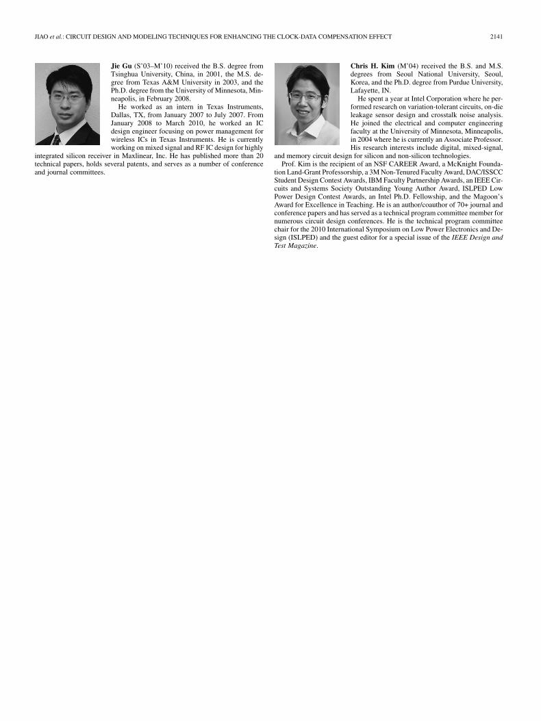
B. Partially Phase-Shifted Clock Distribution Design
Since the phase-shifted clock buffers are larger than (or havelower drive current than) conventional buffers, a more econom-ical approach would be to limit their use to global clock bufferstages. We refer to this implementation as the “partially phase-shifted design” which is illustrated in Fig. 28. Simulation re-sults of the worst-case slack are shown in Fig. 29 for differentnumbers of global clock buffer stages using the stacked LVTbuffers. Since the number of buffers at each clock hierarchy in-creases exponentially in an H-tree type topology, the area over-head can be significantly reduced by using conventional buffersin the final stages of the clock network. As shown in Fig. 29,using phase-shifted clock buffers in the first 9 out of 11 stagesin the clock network can provide a 52 ps improvement in theworst-case slack (about 71% of the maximal possible improve-ment) while reducing the clock buffer area overhead by 75%.
C. Impact of Delay Sensitivity, Process, Temperature andResonant Frequency Variations
Most of the analysis in the previous sections assumes that theclock path and datapath have the same delay sensitivities. In re-ality, the delay sensitivity may vary depending on the amountof interconnect. For example, a clock path may have a lowersensitivity because of its long interconnect, and a datapath mayalso have a low sensitivity if it is wire dominated, like in databuses. To verify the performance of the phase-shifted clock dis-tribution technique for different delay sensitivities, we presentsimulation results of the worst-case slack where the delay sen-sitivity of the datapath is fixed at 2 while the delay sensitivity ofthe clock path is swept from 1.6 to 2.4. The figure clearly showsthat the worst-case slack is improved using the proposed clockbuffer for the entire delay sensitivity range. Also shown are the

2140 IEEE JOURNAL OF SOLID-STATE CIRCUITS, VOL. 45, NO. 10, OCTOBER 2010
Fig. 30. Impact of random process variation on the worst-case slack at 25 Cand 110 C. Monte Carlo simulations were performed using the followingparameters:� � ��� � ����,� � ��� � ����, � � ��� � ����,� � ��� � ����.
average and values of the worst-case slack from Monte Carlosimulations with random local and variations. Despitethe slight degradation in the timing slack, the proposed stackedclock buffer design provides a consistent timing improvement inthe presence of random process variation at 25 C and 110 C.
VIII. CONCLUSION
In this paper, we have presented a comprehensive study ofthe clock data compensation effect occuring in the event of res-onant supply noise. A novel phase-shifted clock buffer designwas proposed to enhance the timing compensation between theclock path and the datapath. A 1.2 V, 65 nm test chip demon-strates an 8–27% performance improvement in for typicalresonant noise frequencies from 100 MHz to 300 MHz. Com-pared with the previous RC filtered phase-shifted buffer, our de-sign saves 85% of the clock buffer area while achieving similarperformance improvement. Several practical issues of the pro-posed clock buffers were discussed including comparison withthe adaptive clocking scheme and partially applying the pro-posed phase-shifted clock buffers. A mathematical frameworkwas also proposed to model the timing margin improvements.The proposed numerical method was verified with extensiveHSPICE simulations showing a 4–10 reduction in estimationerror compared with prior modeling techniques.
REFERENCES
[1] M. Saint-Laurent and M. Swaminathan, “Impact of power-supply noiseon timing in high-frequency microprocessors,” IEEE Trans. AdvancedPackaging, vol. 27, no. 1, pp. 135–144, Feb. 2004.
[2] M. D. Pant, P. Pant, and D. S. Wills, “On-chip decoupling capacitor op-timization using architectural level prediction,” IEEE Trans. Very LargeScale Integr. (VLSI) Syst., vol. 10, no. 3, pp. 319–326, Jun. 2002.
[3] J. Xu, P. Hazucha, and M. Huang et al., “On-die supply-resonance sup-pression using band-limited active damping,” in IEEE Int. Solid-StateCircuits Conf. (ISSCC) Dig. Tech. Papers, Feb. 2007, pp. 286–603.
[4] J. Gu, R. Harjani, and C. Kim, “Distributed active decoupling capaci-tors for on-chip supply noise cancellation in digital VLSI circuits,” inSymp. VLSI Circuits Dig., Jun. 2006, pp. 216–217.
[5] M. Mansuri and C. K. Yang, “A low-power adaptive bandwidth PLLand clock buffer with supply-noise compensation,” IEEE J. Solid-StateCircuits, vol. 38, no. 11, pp. 1804–1812, Nov. 2003.
[6] L. H. Chen, M. Marek-Sadowska, and F. Brewer, “Coping with bufferdelay change due to power and ground noise,” in Proc. Des. Autom.Conf. (DAC), Jul. 2002, pp. 860–865.
[7] T. Fischer, J. Desai, B. Doyle, S. Naffziger, and B. Patella, “A 90-nmvariable frequency clock system for a power-managed itanium archi-tecture processor,” IEEE J. Solid-State Circuits, vol. 41, no. 1, pp.218–228, Jan. 2006.
[8] S. Yasuda and S. Fujita, “Compact fault recovering flip-flop withadjusting clock timing triggered by error detection,” in Proc. IEEECustom Integrated Circuits Conf. (CICC), Sep. 2007, pp. 721–724.
[9] N. Agarwal and S. S. Rath, “Low-jitter clock distribution circuit,” USPatent 6,842,136 B1, Jan. 11, 2005.
[10] M. Saint-Laurent, “Clock distribution network using feedback forskew compensation and jitter filtering,” US Patent 7,317,342 B2, Jan.8, 2008.
[11] V. Gutnik and A. Chandrakasan, “Clock distribution circuits andmethods of operating same that use multiple clock circuits connectedby phase detector circuits to generate and synchronize local clocksignals,” US Patent 7,571,359 B2, Aug. 4, 2009.
[12] T. Rahal-Arabi, G. Taylor, M. Ma, and C. Webb, “Design and validationof the Pentium III and Pentium 4 processors power delivery,” in Symp.VLSI Circuits Dig., Jun. 2002, pp. 220–223.
[13] S. Pant and E. Chiprout, “Power grid physics and implications forCAD,” in Proc. Design Automation Conf. (DAC), Jul. 2006, pp.199–204.
[14] E. Hailu, D. Boerstler, K. Miki, J. Qi, M. Wang, and M. Riley, “A circuitfor reducing large transient current effects on processor power grids,”in IEEE Int. Solid-State Circuits Conf. (ISSCC) Dig. Tech. Papers, Feb.2006, pp. 2238–2245.
[15] N. Kurd, P. Mosalikanti, M. Neidengard, J. Douglas, and R. Kumar,“Next generation Intel core micro-architecture (Nehalem) clocking,”IEEE J. Solid-State Circuits, vol. 44, no. 4, pp. 1121–1129, Apr. 2009.
[16] T. Rahal-Arabi, G. Taylor, J. Barkatullah, K. L. Wong, and M. Ma, “En-hancing microprocessor immunity to power supply noise with clock/data compensation,” in Symp. VLSI Circuits Dig., Jun. 2005, pp. 16–19.
[17] K. L. Wong, T. Rahal-Arabi, M. Ma, and G. Taylor, “Enhancing mi-croprocessor immunity to power supply noise with clock-data compen-sation,” IEEE J. Solid-State Circuits, vol. 41, no. 4, pp. 749–758, Apr.2006.
[18] J. Gu, H. Eom, and C. H. Kim, “A switched decoupling capacitor circuitfor on-chip supply resonance damping,” in Symp. VLSI Circuits Dig.,2007, pp. 126–127.
[19] D. Jiao, J. Gu, P. Jain, and C. Kim, “Enhancing beneficial jitter usingphase-shifted clock distribution,” in Proc. IEEE Int. Symp. Low PowerElectronics and Design (ISLPED), Aug. 2008, pp. 21–26.
[20] N. Kurd, J. Barkatullah, and P. Madland, “Adaptive frequency clockgeneration system,” US Patent 7,042,259 B2, May 9, 2006.
[21] N. A. Kurd, J. S. Barkarullah, R. O. Dizon, T. D. Fletcher, and P.D. Madland, “A multigigahertz clocking scheme for the Pentium 4microprocessor,” IEEE J. Solid-State Circuits, vol. 36, no. 11, pp.1647–1653, Nov. 2001.
[22] J. M. Hart, K. T. Lee, and D. Chen et al., “Implementation of a fourth-generation 1.8-GHz dual-core SPARC V9 microprocessor,” IEEE J.Solid-State Circuits, vol. 41, no. 1, pp. 210–217, Jan. 2006.
Dong Jiao received the B.S. degree in electrical en-gineering from Tsinghua University, Beijing, China,in 2006, and the M.S. degree in electrical and com-puter engineering from the University of Minnesota,Minneapolis, in 2009, where he is currently pursuingthe Ph.D. degree.
He spent the summer of 2008 working as an internwith Seagate involved in MRAM design and simula-tion. His research interests include power integrity formixed-signal ICs and low-power digital and SRAMdesign.
JIAO et al.: CIRCUIT DESIGN AND MODELING TECHNIQUES FOR ENHANCING THE CLOCK-DATA COMPENSATION EFFECT 2141
Jie Gu (S’03–M’10) received the B.S. degree fromTsinghua University, China, in 2001, the M.S. de-gree from Texas A&M University in 2003, and thePh.D. degree from the University of Minnesota, Min-neapolis, in February 2008.
He worked as an intern in Texas Instruments,Dallas, TX, from January 2007 to July 2007. FromJanuary 2008 to March 2010, he worked an ICdesign engineer focusing on power management forwireless ICs in Texas Instruments. He is currentlyworking on mixed signal and RF IC design for highly
integrated silicon receiver in Maxlinear, Inc. He has published more than 20technical papers, holds several patents, and serves as a number of conferenceand journal committees.
Chris H. Kim (M’04) received the B.S. and M.S.degrees from Seoul National University, Seoul,Korea, and the Ph.D. degree from Purdue University,Lafayette, IN.
He spent a year at Intel Corporation where he per-formed research on variation-tolerant circuits, on-dieleakage sensor design and crosstalk noise analysis.He joined the electrical and computer engineeringfaculty at the University of Minnesota, Minneapolis,in 2004 where he is currently an Associate Professor.His research interests include digital, mixed-signal,
and memory circuit design for silicon and non-silicon technologies.Prof. Kim is the recipient of an NSF CAREER Award, a McKnight Founda-
tion Land-Grant Professorship, a 3M Non-Tenured Faculty Award, DAC/ISSCCStudent Design Contest Awards, IBM Faculty Partnership Awards, an IEEE Cir-cuits and Systems Society Outstanding Young Author Award, ISLPED LowPower Design Contest Awards, an Intel Ph.D. Fellowship, and the Magoon’sAward for Excellence in Teaching. He is an author/coauthor of 70+ journal andconference papers and has served as a technical program committee member fornumerous circuit design conferences. He is the technical program committeechair for the 2010 International Symposium on Low Power Electronics and De-sign (ISLPED) and the guest editor for a special issue of the IEEE Design andTest Magazine.


![A 68 Parallel Row Access Neuromorphic Core with 22K Multi ...people.ece.umn.edu/groups/VLSIresearch/papers/2018/IEDM18_Eflash_slides.pdf · IEDM’17 [2] Weight Resolution YES (ReRAM)](https://img.pdfslide.us/doc/110x75/5e39517ced87f00cdb6af9d5/a-68-parallel-row-access-neuromorphic-core-with-22k-multi-iedma17-2-weight.jpg)