Embed Size (px)
Citation preview
IEEE JOURNAL OF SOLID-STATE CIRCUITS, VOL. 46, NO. 6, JUNE 2011 1495
A 3T Gain Cell Embedded DRAM UtilizingPreferential Boosting for High Density and
Low Power On-Die CachesKi Chul Chun, Pulkit Jain, Jung Hwa Lee, and Chris H. Kim, Senior Member, IEEE
Abstract—Circuit techniques for enabling a sub-0.9 V logic-com-patible embedded DRAM (eDRAM) are presented. A boosted 3Tgain cell utilizes Read Word-line (RWL) preferential boosting toincrease read margin and improve data retention time. Read speedis enhanced with a hybrid current/voltage sense amplifier that al-lows the Read Bit-line (RBL) to remain close to VDD. A regu-lated bit-line write scheme for driving the Write Bit-line (WBL) isequipped with a steady-state storage node voltage monitor to over-come the data ‘1’ write disturbance problem of the PMOS gain cellwithout introducing another boosted supply for the Write Word-line (WWL) over-drive. An adaptive and die-to-die adjustable readreference bias generator is proposed to cope with PVT variations.Monte Carlo simulations compare the 6-sigma read and write per-formance of proposed eDRAM against conventional designs. Mea-surement results from a 64 kb eDRAM test chip implemented in a65 nm low-leakage CMOS process show a 1.25 ms data retentiontime with a 2 ns random cycle time at 0.9 V, 85 C, and a 91.3 Wper Mb static power dissipation at 1.0 V, 85 C.
Index Terms—Cache, logic-compatible eDRAM, low-power,low-voltage, 3T gain cell.
I. INTRODUCTION
P OWER dissipation has become the chief performance lim-iter in modern microprocessors, triggering a flurry of re-
search activities on low-power design techniques. One of themost effective ways to curb chip power is to integrate morememory: a larger cache memory improves micro-architecturalperformance with only a modest increase in power. Asa result, the past decade has seen a precipitous increase in theamount of on-die embedded memory. Approximately half thechip area is devoted to cache memory in state-of-the-art de-signs. For example, Intel’s 8-core Nehalem processor has 24MB of shared L3 cache based on SRAM cells [1] while IBM’sPOWER7 processor has a 32 MB L3 cache built in an em-bedded DRAM (eDRAM) technology [2]. The need for robusthigh-density embedded memories is projected to grow as de-signers continue to seek power-conscious ways to improve chipperformance.In order to maintain the historical growth in chip perfor-
mance, designers must continue to delivery memory solutions
Manuscript received June 14, 2010; revised October 02, 2010; accepted Jan-uary 23, 2011. Date of publication May 05, 2011; date of current version May25, 2011. This paper was approved by Associate Editor Sreedhar Natarajan.K. C. Chun, P. Jain, and C. H. Kim are with the Department of Electrical
and Computer Engineering, University of Minnesota, Minneapolis, MN 55455USA (e-mail: [email protected]).J. H. Lee is with the DRAMDesign Team, Memory Division, Samsung Elec-
tronics, Hwasung, Kyeonggi-Do 445-701, Korea.Digital Object Identifier 10.1109/JSSC.2011.2128150
for achieving low static power and high operating speed.SRAMs have been the embedded memory of choice due totheir logic compatibility and fast access time. Recently, em-bedded DRAMs (eDRAMs) have been gaining popularity inthe research community due to features such as small cell size,low cell leakage, and non-ratioed circuit operation. There havebeen a number of successful eDRAM designs based on tradi-tional 1T1C DRAM cells as well as logic-compatible gain cells[2]–[9]. 1T1C cells are denser than gain cells, but at the cost of acapacitor process, and the noise margin is reduced substantiallyat low voltages as the read operation is based on the chargesharing principle. Gain cells are made of logic devices allowingthem to be built in a standard CMOS process with minimalalteration. The cell can be implemented using three transistors,or even two transistors when used with delicate read controlcircuits, achieving roughly 2x higher bit cell densities thanSRAMs [7]–[9]. Furthermore, gain cells can have smaller cellleakage current than SRAMs in sleep mode due to the smallernumber of devices and the super cut-off biasing condition. Thewrite margin is better than SRAMs since there is no contentionbetween the access device and the cross-coupled latch in aneDRAM cell. Despite these favorable features, conventionalgain cells suffer from short data retention times due to the smallstorage capacitor and various leakage sources in the presence ofprocess–voltage–temperature (PVT) variation [7], [8] requiringcareful margin distribution, cell tracking, and reference voltagecontrol. Short retention times result in larger refresh power andpoor read performance. In this work, we address the aforemen-tioned challenges by proposing various circuit techniques toimprove the data retention time of gain cell based eDRAMs.The remainder of this paper is organized as follows. Section II
introduces the basic operation of a conventional 3T eDRAMgain cell. Section III presents the proposed circuit techniquesto enhance the date retention time and improve the read speedof gain cell eDRAMs. Section IV compares access speeds andpower dissipations of 6T SRAM and 3T eDRAM arrays by run-ning Monte Carlo simulations. Section V describes hardwaremeasurement results from a 65 nm test chip. Conclusions aregiven in Section VI.
II. BASIC OPERATION OF A CONVENTIONAL 3T EDRAMGAIN CELL
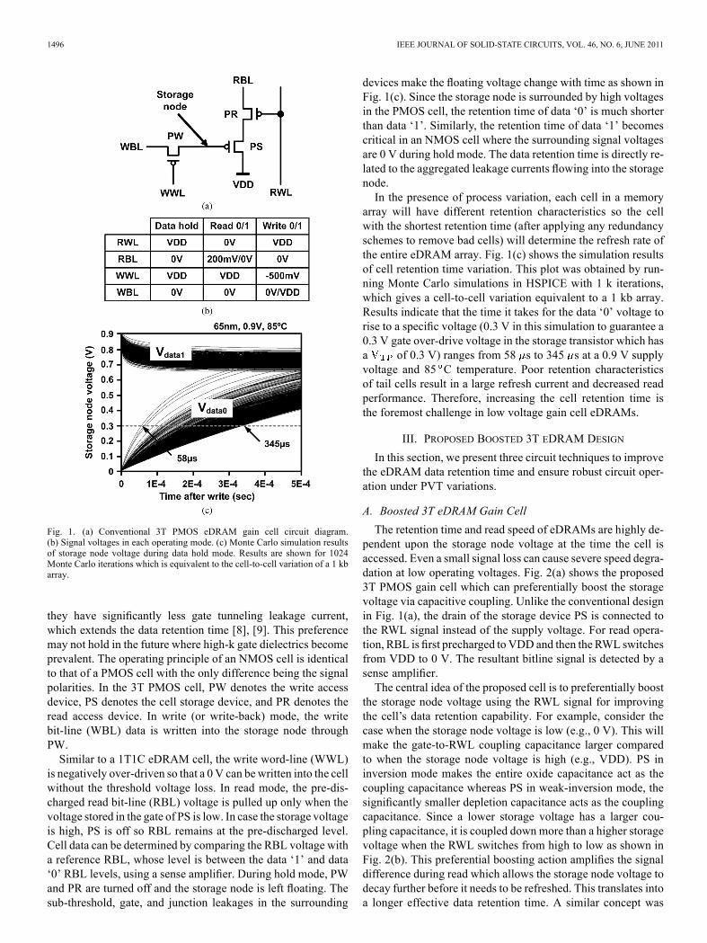
To aid the understanding of our proposed techniques, in thissection, we first describe the basic operation of a conventional3T eDRAM gain cell. Fig. 1(a) shows the cell schematic andFig. 1(b) summarizes the signal conditions for each operatingmode. PMOS devices are chosen over NMOS devices because
0018-9200/$26.00 © 2011 IEEE
1496 IEEE JOURNAL OF SOLID-STATE CIRCUITS, VOL. 46, NO. 6, JUNE 2011
Fig. 1. (a) Conventional 3T PMOS eDRAM gain cell circuit diagram.(b) Signal voltages in each operating mode. (c) Monte Carlo simulation resultsof storage node voltage during data hold mode. Results are shown for 1024Monte Carlo iterations which is equivalent to the cell-to-cell variation of a 1 kbarray.
they have significantly less gate tunneling leakage current,which extends the data retention time [8], [9]. This preferencemay not hold in the future where high-k gate dielectrics becomeprevalent. The operating principle of an NMOS cell is identicalto that of a PMOS cell with the only difference being the signalpolarities. In the 3T PMOS cell, PW denotes the write accessdevice, PS denotes the cell storage device, and PR denotes theread access device. In write (or write-back) mode, the writebit-line (WBL) data is written into the storage node throughPW.Similar to a 1T1C eDRAM cell, the write word-line (WWL)
is negatively over-driven so that a 0 V can be written into the cellwithout the threshold voltage loss. In read mode, the pre-dis-charged read bit-line (RBL) voltage is pulled up only when thevoltage stored in the gate of PS is low. In case the storage voltageis high, PS is off so RBL remains at the pre-discharged level.Cell data can be determined by comparing the RBL voltage witha reference RBL, whose level is between the data ‘1’ and data‘0’ RBL levels, using a sense amplifier. During hold mode, PWand PR are turned off and the storage node is left floating. Thesub-threshold, gate, and junction leakages in the surrounding
devices make the floating voltage change with time as shown inFig. 1(c). Since the storage node is surrounded by high voltagesin the PMOS cell, the retention time of data ‘0’ is much shorterthan data ‘1’. Similarly, the retention time of data ‘1’ becomescritical in an NMOS cell where the surrounding signal voltagesare 0 V during hold mode. The data retention time is directly re-lated to the aggregated leakage currents flowing into the storagenode.In the presence of process variation, each cell in a memory
array will have different retention characteristics so the cellwith the shortest retention time (after applying any redundancyschemes to remove bad cells) will determine the refresh rate ofthe entire eDRAM array. Fig. 1(c) shows the simulation resultsof cell retention time variation. This plot was obtained by run-ning Monte Carlo simulations in HSPICE with 1 k iterations,which gives a cell-to-cell variation equivalent to a 1 kb array.Results indicate that the time it takes for the data ‘0’ voltage torise to a specific voltage (0.3 V in this simulation to guarantee a0.3 V gate over-drive voltage in the storage transistor which hasa of 0.3 V) ranges from 58 s to 345 s at a 0.9 V supplyvoltage and 85 C temperature. Poor retention characteristicsof tail cells result in a large refresh current and decreased readperformance. Therefore, increasing the cell retention time isthe foremost challenge in low voltage gain cell eDRAMs.
III. PROPOSED BOOSTED 3T EDRAM DESIGN
In this section, we present three circuit techniques to improvethe eDRAM data retention time and ensure robust circuit oper-ation under PVT variations.
A. Boosted 3T eDRAM Gain Cell
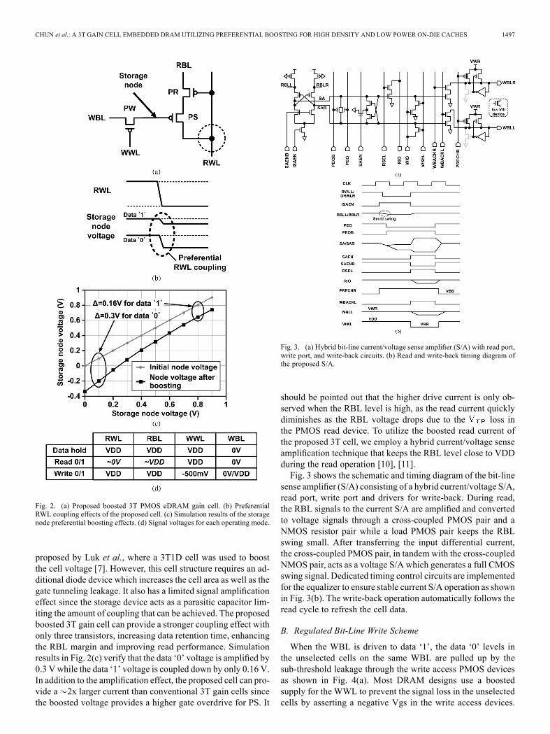
The retention time and read speed of eDRAMs are highly de-pendent upon the storage node voltage at the time the cell isaccessed. Even a small signal loss can cause severe speed degra-dation at low operating voltages. Fig. 2(a) shows the proposed3T PMOS gain cell which can preferentially boost the storagevoltage via capacitive coupling. Unlike the conventional designin Fig. 1(a), the drain of the storage device PS is connected tothe RWL signal instead of the supply voltage. For read opera-tion, RBL is first precharged to VDD and then the RWL switchesfrom VDD to 0 V. The resultant bitline signal is detected by asense amplifier.The central idea of the proposed cell is to preferentially boost
the storage node voltage using the RWL signal for improvingthe cell’s data retention capability. For example, consider thecase when the storage node voltage is low (e.g., 0 V). This willmake the gate-to-RWL coupling capacitance larger comparedto when the storage node voltage is high (e.g., VDD). PS ininversion mode makes the entire oxide capacitance act as thecoupling capacitance whereas PS in weak-inversion mode, thesignificantly smaller depletion capacitance acts as the couplingcapacitance. Since a lower storage voltage has a larger cou-pling capacitance, it is coupled down more than a higher storagevoltage when the RWL switches from high to low as shown inFig. 2(b). This preferential boosting action amplifies the signaldifference during read which allows the storage node voltage todecay further before it needs to be refreshed. This translates intoa longer effective data retention time. A similar concept was
CHUN et al.: A 3T GAIN CELL EMBEDDED DRAM UTILIZING PREFERENTIAL BOOSTING FOR HIGH DENSITY AND LOW POWER ON-DIE CACHES 1497
Fig. 2. (a) Proposed boosted 3T PMOS eDRAM gain cell. (b) PreferentialRWL coupling effects of the proposed cell. (c) Simulation results of the storagenode preferential boosting effects. (d) Signal voltages for each operating mode.
proposed by Luk et al., where a 3T1D cell was used to boostthe cell voltage [7]. However, this cell structure requires an ad-ditional diode device which increases the cell area as well as thegate tunneling leakage. It also has a limited signal amplificationeffect since the storage device acts as a parasitic capacitor lim-iting the amount of coupling that can be achieved. The proposedboosted 3T gain cell can provide a stronger coupling effect withonly three transistors, increasing data retention time, enhancingthe RBL margin and improving read performance. Simulationresults in Fig. 2(c) verify that the data ‘0’ voltage is amplified by0.3 V while the data ‘1’ voltage is coupled down by only 0.16 V.In addition to the amplification effect, the proposed cell can pro-vide a 2x larger current than conventional 3T gain cells sincethe boosted voltage provides a higher gate overdrive for PS. It
Fig. 3. (a) Hybrid bit-line current/voltage sense amplifier (S/A) with read port,write port, and write-back circuits. (b) Read and write-back timing diagram ofthe proposed S/A.
should be pointed out that the higher drive current is only ob-served when the RBL level is high, as the read current quicklydiminishes as the RBL voltage drops due to the loss inthe PMOS read device. To utilize the boosted read current ofthe proposed 3T cell, we employ a hybrid current/voltage senseamplification technique that keeps the RBL level close to VDDduring the read operation [10], [11].Fig. 3 shows the schematic and timing diagram of the bit-line
sense amplifier (S/A) consisting of a hybrid current/voltage S/A,read port, write port and drivers for write-back. During read,the RBL signals to the current S/A are amplified and convertedto voltage signals through a cross-coupled PMOS pair and aNMOS resistor pair while a load PMOS pair keeps the RBLswing small. After transferring the input differential current,the cross-coupled PMOS pair, in tandem with the cross-coupledNMOS pair, acts as a voltage S/A which generates a full CMOSswing signal. Dedicated timing control circuits are implementedfor the equalizer to ensure stable current S/A operation as shownin Fig. 3(b). The write-back operation automatically follows theread cycle to refresh the cell data.
B. Regulated Bit-Line Write Scheme
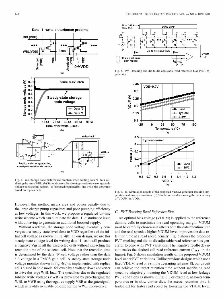
When the WBL is driven to data ‘1’, the data ‘0’ levels inthe unselected cells on the same WBL are pulled up by thesub-threshold leakage through the write access PMOS devicesas shown in Fig. 4(a). Most DRAM designs use a boostedsupply for the WWL to prevent the signal loss in the unselectedcells by asserting a negative Vgs in the write access devices.
1498 IEEE JOURNAL OF SOLID-STATE CIRCUITS, VOL. 46, NO. 6, JUNE 2011
Fig. 4. (a) Storage node disturbance problem when writing data ‘1’ to a cellsharing the sameWBL. (b) Simulation results showing steady-state storage nodevoltage in case of no refresh. (c) Proposed regulated bit-line write bias generatorbased on replica cells.
However, this method incurs area and power penalty due tothe large charge pump capacitors and poor pumping efficiencyat low voltages. In this work, we propose a regulated bit-linewrite scheme which can eliminate the data ‘1’ disturbance issuewithout having to generate an additional boosted supply.Without a refresh, the storage node voltage eventually con-
verges to a steady-state level close to VDD regardless of the ini-tial cell voltage as shown in Fig. 4(b). In our design, we use thissteady-state voltage level for writing data ‘1’, as it will producea negative Vgs in all the unselected cells without impacting theretention time of the selected cell. Note that the retention timeis determined by the data ‘0’ cell voltage rather than the data‘1’ voltage in a PMOS gain cell. A steady-state storage nodevoltage monitor shown in Fig. 4(c) is implemented with replicacells biased in hold mode, followed by a voltage down converterto drive the large WBL load. The speed loss due to the regulatedbit-line write voltage (VWR) is prevented by pre-charging theWBL to VWR using the negative supply VBB as the gate signal,which is readily available on-chip for the WWL under-drive.
Fig. 5. PVT-tracking and die-to-die adjustable read reference bias (VDUM)generator.
Fig. 6. (a) Simulation results of the proposed VDUM generator tracking tem-perature and process variations. (b) Simulation results showing the dependencyof VDUM on VDD.
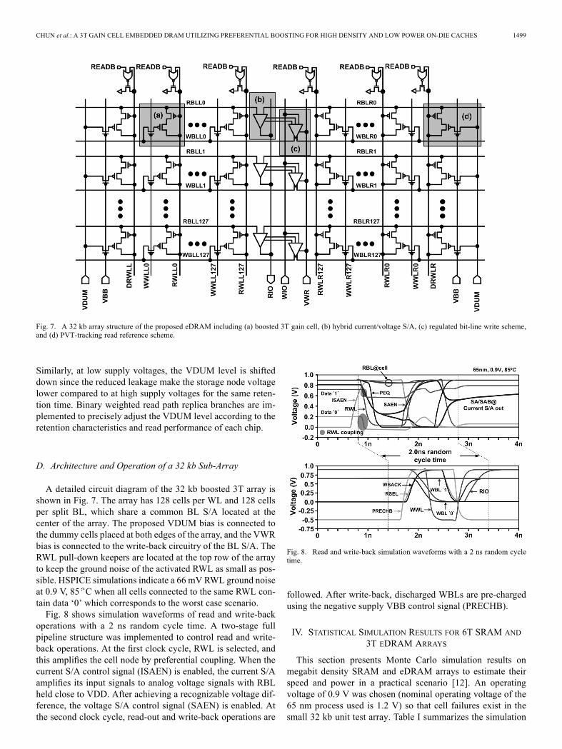
C. PVT-Tracking Read Reference Bias
An optimal bias voltage (VDUM) is applied to the referencedummy cells to maximize the read operating margin. VDUMmust be carefully chosen as it affects both the data retention timeand the read speed; a higher VDUM level improves the data re-tention time at a read speed penalty. Fig. 5 shows the proposedPVT-tracking and die-to-die adjustable read reference bias gen-erator to cope with PVT variations. The negative feedback cir-cuit tracks the desired cell read reference current ( in thefigure). Fig. 6 shows simulation results of the proposed VDUMlevel under PVT variations. Unlike previous designs which use afixed VDUM level or a simple averaging scheme [8], our circuitcan achieve the target retention time without sacrificing readspeed by adaptively lowering the VDUM level at low leakagePVT conditions as shown in Fig. 6. For example, at lower tem-peratures or in slow corner dies, the excess retention time istraded off for faster read speed by lowering the VDUM level.
CHUN et al.: A 3T GAIN CELL EMBEDDED DRAM UTILIZING PREFERENTIAL BOOSTING FOR HIGH DENSITY AND LOW POWER ON-DIE CACHES 1499
Fig. 7. A 32 kb array structure of the proposed eDRAM including (a) boosted 3T gain cell, (b) hybrid current/voltage S/A, (c) regulated bit-line write scheme,and (d) PVT-tracking read reference scheme.
Similarly, at low supply voltages, the VDUM level is shifteddown since the reduced leakage make the storage node voltagelower compared to at high supply voltages for the same reten-tion time. Binary weighted read path replica branches are im-plemented to precisely adjust the VDUM level according to theretention characteristics and read performance of each chip.
D. Architecture and Operation of a 32 kb Sub-Array
A detailed circuit diagram of the 32 kb boosted 3T array isshown in Fig. 7. The array has 128 cells per WL and 128 cellsper split BL, which share a common BL S/A located at thecenter of the array. The proposed VDUM bias is connected tothe dummy cells placed at both edges of the array, and the VWRbias is connected to the write-back circuitry of the BL S/A. TheRWL pull-down keepers are located at the top row of the arrayto keep the ground noise of the activated RWL as small as pos-sible. HSPICE simulations indicate a 66 mV RWL ground noiseat 0.9 V, 85 C when all cells connected to the same RWL con-tain data ‘0’ which corresponds to the worst case scenario.Fig. 8 shows simulation waveforms of read and write-back
operations with a 2 ns random cycle time. A two-stage fullpipeline structure was implemented to control read and write-back operations. At the first clock cycle, RWL is selected, andthis amplifies the cell node by preferential coupling. When thecurrent S/A control signal (ISAEN) is enabled, the current S/Aamplifies its input signals to analog voltage signals with RBLheld close to VDD. After achieving a recognizable voltage dif-ference, the voltage S/A control signal (SAEN) is enabled. Atthe second clock cycle, read-out and write-back operations are
Fig. 8. Read and write-back simulation waveforms with a 2 ns random cycletime.
followed. After write-back, discharged WBLs are pre-chargedusing the negative supply VBB control signal (PRECHB).
IV. STATISTICAL SIMULATION RESULTS FOR 6T SRAM AND
3T EDRAM ARRAYS
This section presents Monte Carlo simulation results onmegabit density SRAM and eDRAM arrays to estimate theirspeed and power in a practical scenario [12]. An operatingvoltage of 0.9 V was chosen (nominal operating voltage of the65 nm process used is 1.2 V) so that cell failures exist in thesmall 32 kb unit test array. Table I summarizes the simulation
1500 IEEE JOURNAL OF SOLID-STATE CIRCUITS, VOL. 46, NO. 6, JUNE 2011
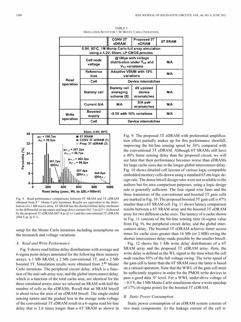
TABLE ISIMULATION SETUP FOR 1 M MONTE CARLO ITERATIONS
Fig. 9. Read performance comparisons between 6T SRAM and 3T eDRAMobtained from Monte Carlo iterations. Results are equivalent to the distri-bution of a 1 Mb macro array. 6T SRAM has the shortest bitline delay attributedto the differential swing nature and large drive current (361.7 ps@ ) followedby the proposed 3T eDRAM (607.4 ps @ ) and the conventional 3T eDRAM(944.5 ps @ ).
setup for the Monte Carlo iterations including assumptions onthe mismatch and voltage variations.
A. Read and Write Performance
Fig. 9 shows read bitline delay distributions with average and6-sigma point delays annotated for the following three memoryarrays; a 1 Mb SRAM, a 2 Mb conventional 3T, and a 2 Mbboosted 3T. Simulation results were obtained from 2 MonteCarlo iterations. The peripheral circuit delay, which is a func-tion of the unit sub-array size, and the global interconnect delay,which is a function of the total cache area, are identical for thethree simulated arrays since we selected an SRAMwith half thenumber of cells as the eDRAMs. Recall that an SRAM bitcellis about twice the area of an eDRAM bitcell. The single-endedsensing nature and the gradual loss in the storage node voltageof the conventional 3T eDRAM result in a 6-sigma read bit-linedelay that is 2.6 times longer than a 6T SRAM as shown in
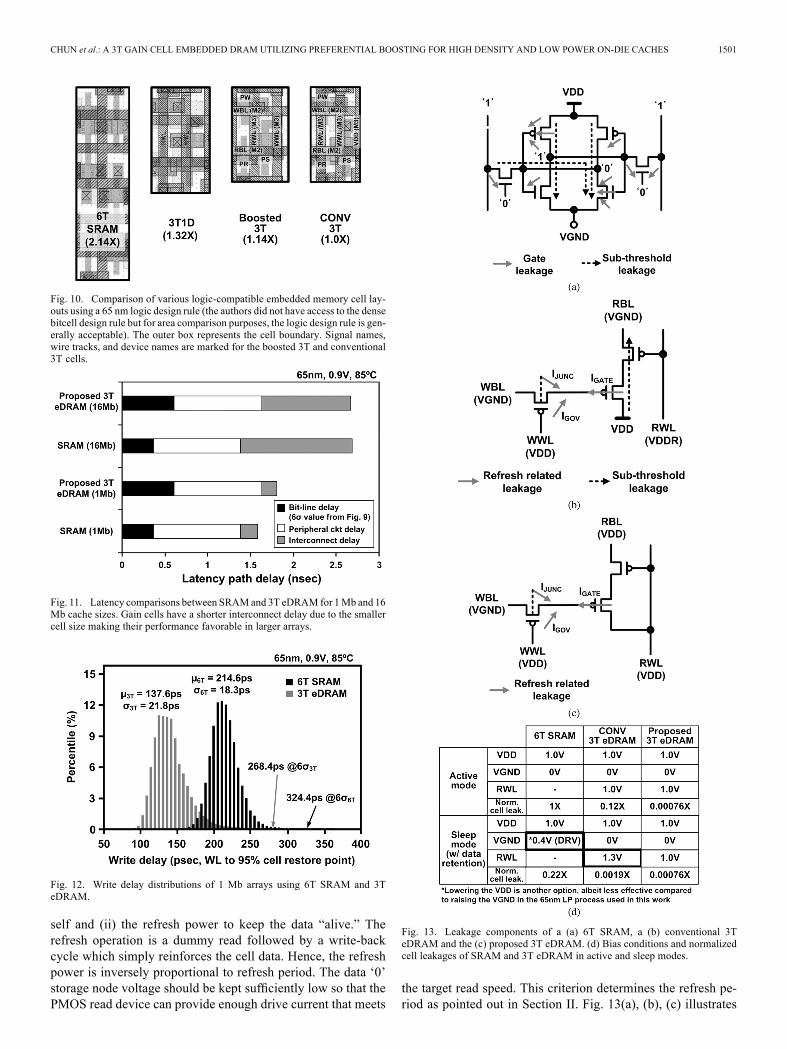
Fig. 9. The proposed 3T eDRAM with preferential amplifica-tion effect partially makes up for this performance shortfall,improving the bit-line sensing speed by 36% compared withthe conventional 3T eDRAM. Although 6T SRAMs still havea 40% faster sensing delay than the proposed circuit, we willsee later that their performance becomes worse than eDRAMsfor large cache sizes due to the longer global interconnect delay.Fig. 10 shows detailed cell layouts of various logic-compatibleembedded memory cells drawn using a standard 65 nm logic de-sign rule. The dense bitcell design rules were not available to theauthors but for area comparison purposes, using a logic designrule is generally sufficient. The four signal wire lines and thethree transistors of the conventional and boosted 3T gain cellsare marked in Fig. 10. The proposed boosted 3T gain cell is 47%smaller than a 6T SRAM cell. Fig. 11 shows latency comparisonresults between a 6T SRAM array and the boosted 3T eDRAMarray for two different cache sizes. The latency of a cache shownin Fig. 11 consists of the bit-line sensing time (6-sigma valuefrom Fig. 9), the peripheral circuit delay, and the global inter-connect delay. The boosted 3T eDRAM achieves faster accesstimes for cache sizes greater than 16 Mb (or 2 MB) owing theshorter interconnect delay made possible by the smaller bitcell.Fig. 12 shows the 1 Mb write delay distributions of a 6T
SRAM array and the proposed 3T eDRAM array. Here, thewrite delay is defined as the WL signal to the time when the cellnode reaches 95% of the full voltage swing. The write speed ofthe gain cell is faster than the 6T SRAM since the latter is basedon a ratioed operation. Note that the WWL of the gain cell mustbe sufficiently negative in order for the PMOS write devices topass a good data ‘0’ level. For a WWL under-drive voltage of0.5 V, the 1MbMonte Carlo simulations show awrite speedup
of 17% (6-sigma point) for the boosted 3T eDRAM.
B. Static Power Consumption
Static power consumption of an eDRAM system consists oftwo main components: (i) the leakage current of the cell it-
CHUN et al.: A 3T GAIN CELL EMBEDDED DRAM UTILIZING PREFERENTIAL BOOSTING FOR HIGH DENSITY AND LOW POWER ON-DIE CACHES 1501
Fig. 10. Comparison of various logic-compatible embedded memory cell lay-outs using a 65 nm logic design rule (the authors did not have access to the densebitcell design rule but for area comparison purposes, the logic design rule is gen-erally acceptable). The outer box represents the cell boundary. Signal names,wire tracks, and device names are marked for the boosted 3T and conventional3T cells.
Fig. 11. Latency comparisons between SRAMand 3T eDRAM for 1Mb and 16Mb cache sizes. Gain cells have a shorter interconnect delay due to the smallercell size making their performance favorable in larger arrays.
Fig. 12. Write delay distributions of 1 Mb arrays using 6T SRAM and 3TeDRAM.
self and (ii) the refresh power to keep the data “alive.” Therefresh operation is a dummy read followed by a write-backcycle which simply reinforces the cell data. Hence, the refreshpower is inversely proportional to refresh period. The data ‘0’storage node voltage should be kept sufficiently low so that thePMOS read device can provide enough drive current that meets
Fig. 13. Leakage components of a (a) 6T SRAM, a (b) conventional 3TeDRAM and the (c) proposed 3T eDRAM. (d) Bias conditions and normalizedcell leakages of SRAM and 3T eDRAM in active and sleep modes.
the target read speed. This criterion determines the refresh pe-riod as pointed out in Section II. Fig. 13(a), (b), (c) illustrates
1502 IEEE JOURNAL OF SOLID-STATE CIRCUITS, VOL. 46, NO. 6, JUNE 2011
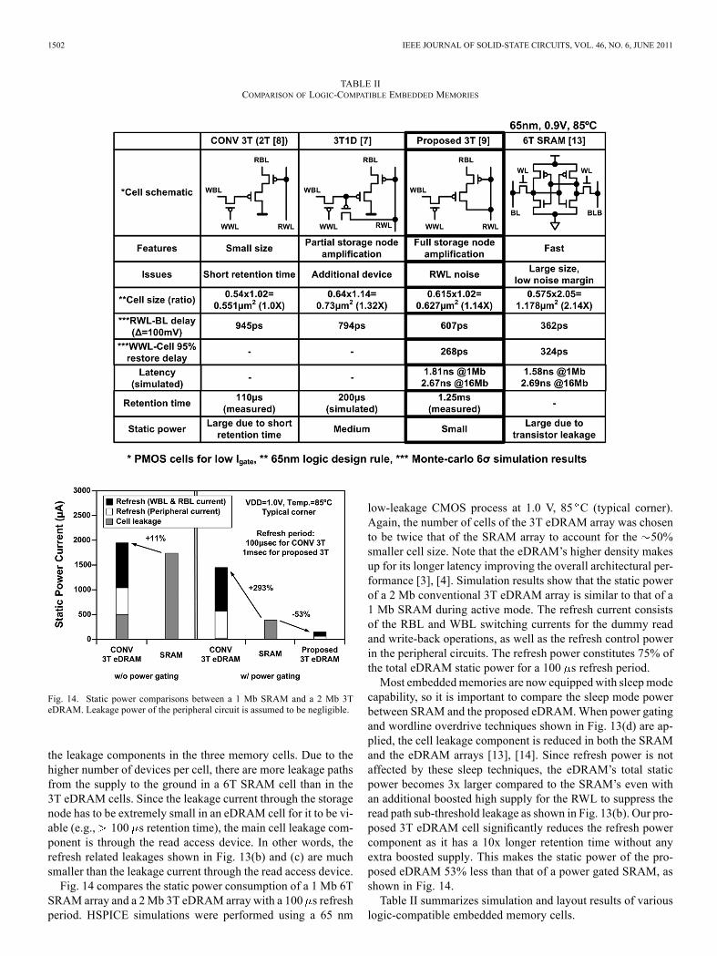
TABLE IICOMPARISON OF LOGIC-COMPATIBLE EMBEDDED MEMORIES
Fig. 14. Static power comparisons between a 1 Mb SRAM and a 2 Mb 3TeDRAM. Leakage power of the peripheral circuit is assumed to be negligible.
the leakage components in the three memory cells. Due to thehigher number of devices per cell, there are more leakage pathsfrom the supply to the ground in a 6T SRAM cell than in the3T eDRAM cells. Since the leakage current through the storagenode has to be extremely small in an eDRAM cell for it to be vi-able (e.g., 100 s retention time), the main cell leakage com-ponent is through the read access device. In other words, therefresh related leakages shown in Fig. 13(b) and (c) are muchsmaller than the leakage current through the read access device.Fig. 14 compares the static power consumption of a 1 Mb 6T
SRAM array and a 2Mb 3T eDRAM array with a 100 s refreshperiod. HSPICE simulations were performed using a 65 nm
low-leakage CMOS process at 1.0 V, 85 C (typical corner).Again, the number of cells of the 3T eDRAM array was chosento be twice that of the SRAM array to account for the 50%smaller cell size. Note that the eDRAM’s higher density makesup for its longer latency improving the overall architectural per-formance [3], [4]. Simulation results show that the static powerof a 2 Mb conventional 3T eDRAM array is similar to that of a1 Mb SRAM during active mode. The refresh current consistsof the RBL and WBL switching currents for the dummy readand write-back operations, as well as the refresh control powerin the peripheral circuits. The refresh power constitutes 75% ofthe total eDRAM static power for a 100 s refresh period.Most embeddedmemories are now equipped with sleepmode
capability, so it is important to compare the sleep mode powerbetween SRAM and the proposed eDRAM.When power gatingand wordline overdrive techniques shown in Fig. 13(d) are ap-plied, the cell leakage component is reduced in both the SRAMand the eDRAM arrays [13], [14]. Since refresh power is notaffected by these sleep techniques, the eDRAM’s total staticpower becomes 3x larger compared to the SRAM’s even withan additional boosted high supply for the RWL to suppress theread path sub-threshold leakage as shown in Fig. 13(b). Our pro-posed 3T eDRAM cell significantly reduces the refresh powercomponent as it has a 10x longer retention time without anyextra boosted supply. This makes the static power of the pro-posed eDRAM 53% less than that of a power gated SRAM, asshown in Fig. 14.Table II summarizes simulation and layout results of various
logic-compatible embedded memory cells.
CHUN et al.: A 3T GAIN CELL EMBEDDED DRAM UTILIZING PREFERENTIAL BOOSTING FOR HIGH DENSITY AND LOW POWER ON-DIE CACHES 1503
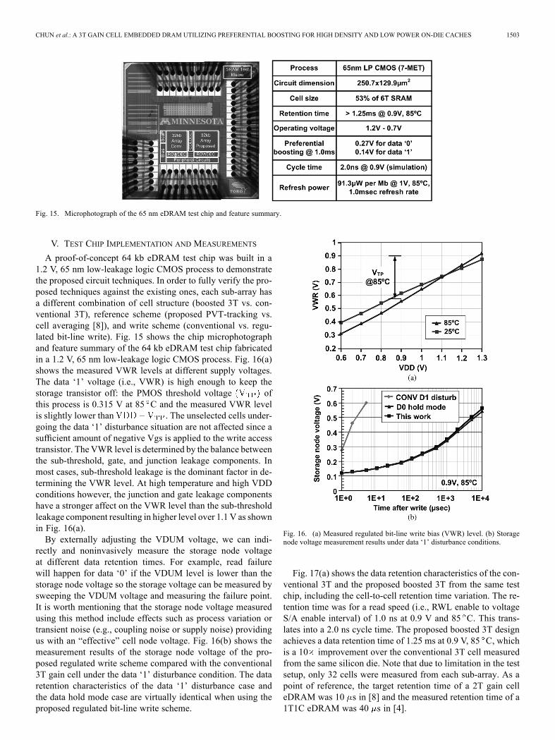
Fig. 15. Microphotograph of the 65 nm eDRAM test chip and feature summary.
V. TEST CHIP IMPLEMENTATION AND MEASUREMENTS
A proof-of-concept 64 kb eDRAM test chip was built in a1.2 V, 65 nm low-leakage logic CMOS process to demonstratethe proposed circuit techniques. In order to fully verify the pro-posed techniques against the existing ones, each sub-array hasa different combination of cell structure (boosted 3T vs. con-ventional 3T), reference scheme (proposed PVT-tracking vs.cell averaging [8]), and write scheme (conventional vs. regu-lated bit-line write). Fig. 15 shows the chip microphotographand feature summary of the 64 kb eDRAM test chip fabricatedin a 1.2 V, 65 nm low-leakage logic CMOS process. Fig. 16(a)shows the measured VWR levels at different supply voltages.The data ‘1’ voltage (i.e., VWR) is high enough to keep thestorage transistor off: the PMOS threshold voltage ofthis process is 0.315 V at 85 C and the measured VWR levelis slightly lower than . The unselected cells under-going the data ‘1’ disturbance situation are not affected since asufficient amount of negative Vgs is applied to the write accesstransistor. The VWR level is determined by the balance betweenthe sub-threshold, gate, and junction leakage components. Inmost cases, sub-threshold leakage is the dominant factor in de-termining the VWR level. At high temperature and high VDDconditions however, the junction and gate leakage componentshave a stronger affect on the VWR level than the sub-thresholdleakage component resulting in higher level over 1.1 V as shownin Fig. 16(a).By externally adjusting the VDUM voltage, we can indi-
rectly and noninvasively measure the storage node voltageat different data retention times. For example, read failurewill happen for data ‘0’ if the VDUM level is lower than thestorage node voltage so the storage voltage can be measured bysweeping the VDUM voltage and measuring the failure point.It is worth mentioning that the storage node voltage measuredusing this method include effects such as process variation ortransient noise (e.g., coupling noise or supply noise) providingus with an “effective” cell node voltage. Fig. 16(b) shows themeasurement results of the storage node voltage of the pro-posed regulated write scheme compared with the conventional3T gain cell under the data ‘1’ disturbance condition. The dataretention characteristics of the data ‘1’ disturbance case andthe data hold mode case are virtually identical when using theproposed regulated bit-line write scheme.
Fig. 16. (a) Measured regulated bit-line write bias (VWR) level. (b) Storagenode voltage measurement results under data ‘1’ disturbance conditions.
Fig. 17(a) shows the data retention characteristics of the con-ventional 3T and the proposed boosted 3T from the same testchip, including the cell-to-cell retention time variation. The re-tention time was for a read speed (i.e., RWL enable to voltageS/A enable interval) of 1.0 ns at 0.9 V and 85 C. This trans-lates into a 2.0 ns cycle time. The proposed boosted 3T designachieves a data retention time of 1.25 ms at 0.9 V, 85 C, whichis a 10 improvement over the conventional 3T cell measuredfrom the same silicon die. Note that due to limitation in the testsetup, only 32 cells were measured from each sub-array. As apoint of reference, the target retention time of a 2T gain celleDRAM was 10 s in [8] and the measured retention time of a1T1C eDRAM was 40 s in [4].
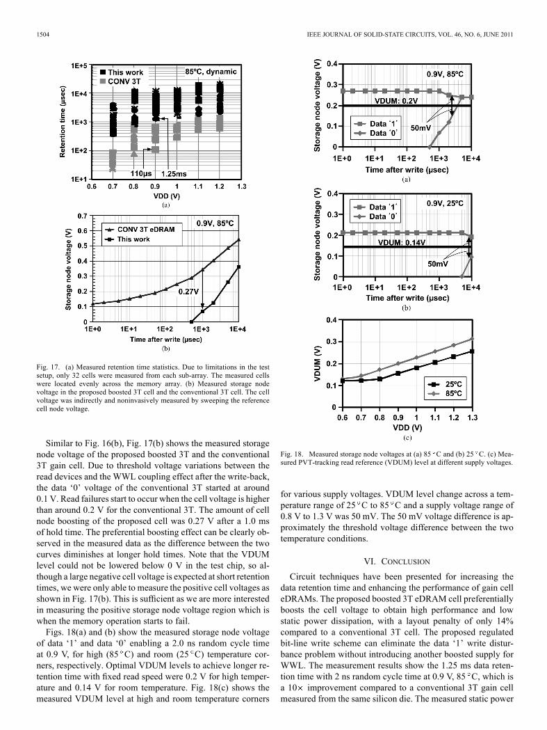
1504 IEEE JOURNAL OF SOLID-STATE CIRCUITS, VOL. 46, NO. 6, JUNE 2011
Fig. 17. (a) Measured retention time statistics. Due to limitations in the testsetup, only 32 cells were measured from each sub-array. The measured cellswere located evenly across the memory array. (b) Measured storage nodevoltage in the proposed boosted 3T cell and the conventional 3T cell. The cellvoltage was indirectly and noninvasively measured by sweeping the referencecell node voltage.
Similar to Fig. 16(b), Fig. 17(b) shows the measured storagenode voltage of the proposed boosted 3T and the conventional3T gain cell. Due to threshold voltage variations between theread devices and the WWL coupling effect after the write-back,the data ‘0’ voltage of the conventional 3T started at around0.1 V. Read failures start to occur when the cell voltage is higherthan around 0.2 V for the conventional 3T. The amount of cellnode boosting of the proposed cell was 0.27 V after a 1.0 msof hold time. The preferential boosting effect can be clearly ob-served in the measured data as the difference between the twocurves diminishes at longer hold times. Note that the VDUMlevel could not be lowered below 0 V in the test chip, so al-though a large negative cell voltage is expected at short retentiontimes, we were only able to measure the positive cell voltages asshown in Fig. 17(b). This is sufficient as we are more interestedin measuring the positive storage node voltage region which iswhen the memory operation starts to fail.Figs. 18(a) and (b) show the measured storage node voltage
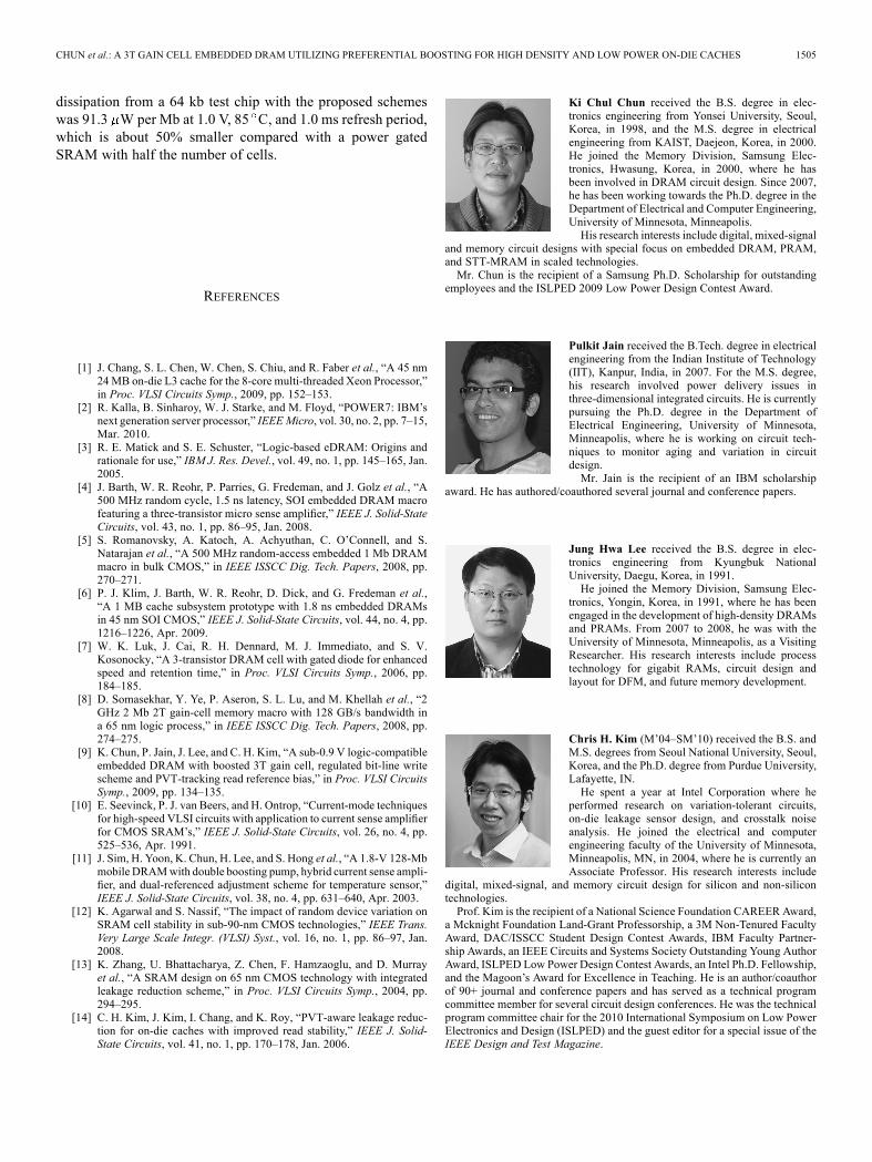
of data ‘1’ and data ‘0’ enabling a 2.0 ns random cycle timeat 0.9 V, for high (85 C) and room (25 C) temperature cor-ners, respectively. Optimal VDUM levels to achieve longer re-tention time with fixed read speed were 0.2 V for high temper-ature and 0.14 V for room temperature. Fig. 18(c) shows themeasured VDUM level at high and room temperature corners
Fig. 18. Measured storage node voltages at (a) 85 C and (b) 25 C. (c) Mea-sured PVT-tracking read reference (VDUM) level at different supply voltages.
for various supply voltages. VDUM level change across a tem-perature range of 25 C to 85 C and a supply voltage range of0.8 V to 1.3 V was 50 mV. The 50 mV voltage difference is ap-proximately the threshold voltage difference between the twotemperature conditions.
VI. CONCLUSION
Circuit techniques have been presented for increasing thedata retention time and enhancing the performance of gain celleDRAMs. The proposed boosted 3T eDRAM cell preferentiallyboosts the cell voltage to obtain high performance and lowstatic power dissipation, with a layout penalty of only 14%compared to a conventional 3T cell. The proposed regulatedbit-line write scheme can eliminate the data ‘1’ write distur-bance problem without introducing another boosted supply forWWL. The measurement results show the 1.25 ms data reten-tion time with 2 ns random cycle time at 0.9 V, 85 C, which isa 10 improvement compared to a conventional 3T gain cellmeasured from the same silicon die. The measured static power
CHUN et al.: A 3T GAIN CELL EMBEDDED DRAM UTILIZING PREFERENTIAL BOOSTING FOR HIGH DENSITY AND LOW POWER ON-DIE CACHES 1505
dissipation from a 64 kb test chip with the proposed schemeswas 91.3 W per Mb at 1.0 V, 85 C, and 1.0 ms refresh period,which is about 50% smaller compared with a power gatedSRAM with half the number of cells.
REFERENCES
[1] J. Chang, S. L. Chen, W. Chen, S. Chiu, and R. Faber et al., “A 45 nm24MB on-die L3 cache for the 8-core multi-threaded Xeon Processor,”in Proc. VLSI Circuits Symp., 2009, pp. 152–153.
[2] R. Kalla, B. Sinharoy, W. J. Starke, and M. Floyd, “POWER7: IBM’snext generation server processor,” IEEEMicro, vol. 30, no. 2, pp. 7–15,Mar. 2010.
[3] R. E. Matick and S. E. Schuster, “Logic-based eDRAM: Origins andrationale for use,” IBM J. Res. Devel., vol. 49, no. 1, pp. 145–165, Jan.2005.
[4] J. Barth, W. R. Reohr, P. Parries, G. Fredeman, and J. Golz et al., “A500 MHz random cycle, 1.5 ns latency, SOI embedded DRAM macrofeaturing a three-transistor micro sense amplifier,” IEEE J. Solid-StateCircuits, vol. 43, no. 1, pp. 86–95, Jan. 2008.
[5] S. Romanovsky, A. Katoch, A. Achyuthan, C. O’Connell, and S.Natarajan et al., “A 500 MHz random-access embedded 1 Mb DRAMmacro in bulk CMOS,” in IEEE ISSCC Dig. Tech. Papers, 2008, pp.270–271.
[6] P. J. Klim, J. Barth, W. R. Reohr, D. Dick, and G. Fredeman et al.,“A 1 MB cache subsystem prototype with 1.8 ns embedded DRAMsin 45 nm SOI CMOS,” IEEE J. Solid-State Circuits, vol. 44, no. 4, pp.1216–1226, Apr. 2009.
[7] W. K. Luk, J. Cai, R. H. Dennard, M. J. Immediato, and S. V.Kosonocky, “A 3-transistor DRAM cell with gated diode for enhancedspeed and retention time,” in Proc. VLSI Circuits Symp., 2006, pp.184–185.
[8] D. Somasekhar, Y. Ye, P. Aseron, S. L. Lu, and M. Khellah et al., “2GHz 2 Mb 2T gain-cell memory macro with 128 GB/s bandwidth ina 65 nm logic process,” in IEEE ISSCC Dig. Tech. Papers, 2008, pp.274–275.
[9] K. Chun, P. Jain, J. Lee, and C. H. Kim, “A sub-0.9 V logic-compatibleembedded DRAM with boosted 3T gain cell, regulated bit-line writescheme and PVT-tracking read reference bias,” in Proc. VLSI CircuitsSymp., 2009, pp. 134–135.
[10] E. Seevinck, P. J. van Beers, and H. Ontrop, “Current-mode techniquesfor high-speed VLSI circuits with application to current sense amplifierfor CMOS SRAM’s,” IEEE J. Solid-State Circuits, vol. 26, no. 4, pp.525–536, Apr. 1991.
[11] J. Sim, H. Yoon, K. Chun, H. Lee, and S. Hong et al., “A 1.8-V 128-Mbmobile DRAMwith double boosting pump, hybrid current sense ampli-fier, and dual-referenced adjustment scheme for temperature sensor,”IEEE J. Solid-State Circuits, vol. 38, no. 4, pp. 631–640, Apr. 2003.
[12] K. Agarwal and S. Nassif, “The impact of random device variation onSRAM cell stability in sub-90-nm CMOS technologies,” IEEE Trans.Very Large Scale Integr. (VLSI) Syst., vol. 16, no. 1, pp. 86–97, Jan.2008.
[13] K. Zhang, U. Bhattacharya, Z. Chen, F. Hamzaoglu, and D. Murrayet al., “A SRAM design on 65 nm CMOS technology with integratedleakage reduction scheme,” in Proc. VLSI Circuits Symp., 2004, pp.294–295.
[14] C. H. Kim, J. Kim, I. Chang, and K. Roy, “PVT-aware leakage reduc-tion for on-die caches with improved read stability,” IEEE J. Solid-State Circuits, vol. 41, no. 1, pp. 170–178, Jan. 2006.
Ki Chul Chun received the B.S. degree in elec-tronics engineering from Yonsei University, Seoul,Korea, in 1998, and the M.S. degree in electricalengineering from KAIST, Daejeon, Korea, in 2000.He joined the Memory Division, Samsung Elec-tronics, Hwasung, Korea, in 2000, where he hasbeen involved in DRAM circuit design. Since 2007,he has been working towards the Ph.D. degree in theDepartment of Electrical and Computer Engineering,University of Minnesota, Minneapolis.His research interests include digital, mixed-signal
and memory circuit designs with special focus on embedded DRAM, PRAM,and STT-MRAM in scaled technologies.Mr. Chun is the recipient of a Samsung Ph.D. Scholarship for outstanding
employees and the ISLPED 2009 Low Power Design Contest Award.
Pulkit Jain received the B.Tech. degree in electricalengineering from the Indian Institute of Technology(IIT), Kanpur, India, in 2007. For the M.S. degree,his research involved power delivery issues inthree-dimensional integrated circuits. He is currentlypursuing the Ph.D. degree in the Department ofElectrical Engineering, University of Minnesota,Minneapolis, where he is working on circuit tech-niques to monitor aging and variation in circuitdesign.Mr. Jain is the recipient of an IBM scholarship
award. He has authored/coauthored several journal and conference papers.
Jung Hwa Lee received the B.S. degree in elec-tronics engineering from Kyungbuk NationalUniversity, Daegu, Korea, in 1991.He joined the Memory Division, Samsung Elec-
tronics, Yongin, Korea, in 1991, where he has beenengaged in the development of high-density DRAMsand PRAMs. From 2007 to 2008, he was with theUniversity of Minnesota, Minneapolis, as a VisitingResearcher. His research interests include processtechnology for gigabit RAMs, circuit design andlayout for DFM, and future memory development.
Chris H. Kim (M’04–SM’10) received the B.S. andM.S. degrees from Seoul National University, Seoul,Korea, and the Ph.D. degree from Purdue University,Lafayette, IN.He spent a year at Intel Corporation where he
performed research on variation-tolerant circuits,on-die leakage sensor design, and crosstalk noiseanalysis. He joined the electrical and computerengineering faculty of the University of Minnesota,Minneapolis, MN, in 2004, where he is currently anAssociate Professor. His research interests include
digital, mixed-signal, and memory circuit design for silicon and non-silicontechnologies.Prof. Kim is the recipient of a National Science Foundation CAREERAward,
a Mcknight Foundation Land-Grant Professorship, a 3M Non-Tenured FacultyAward, DAC/ISSCC Student Design Contest Awards, IBM Faculty Partner-ship Awards, an IEEE Circuits and Systems Society Outstanding Young AuthorAward, ISLPED Low Power Design Contest Awards, an Intel Ph.D. Fellowship,and the Magoon’s Award for Excellence in Teaching. He is an author/coauthorof 90+ journal and conference papers and has served as a technical programcommittee member for several circuit design conferences. He was the technicalprogram committee chair for the 2010 International Symposium on Low PowerElectronics and Design (ISLPED) and the guest editor for a special issue of theIEEE Design and Test Magazine.


![A 68 Parallel Row Access Neuromorphic Core with 22K Multi ...people.ece.umn.edu/groups/VLSIresearch/papers/2018/IEDM18_Eflash_slides.pdf · IEDM’17 [2] Weight Resolution YES (ReRAM)](https://img.pdfslide.us/doc/110x75/5e39517ced87f00cdb6af9d5/a-68-parallel-row-access-neuromorphic-core-with-22k-multi-iedma17-2-weight.jpg)