Embed Size (px)
Citation preview
- 1 -
Width-dependent Statistical Leakage Modeling for Random Dopant Induced Threshold Voltage Shift
Jie Gu Sachin S. Sapatnekar Chris Kim Department of Electrical and Computer Engineering
University of Minnesota, Minneapolis, MN {jiegu, sachin, chriskim}@umn.edu
ABSTRACT Statistical behavior of device leakage and threshold voltage
shows a strong width dependency under microscopic random dopant fluctuation. Leakage estimation using the conventional square-root method shows a discrepancy as large as 45% compared to the real case because it fails to model the effective VT shift in the subthreshold region. This paper presents a width-dependent statistical leakage model with an estimation error less than 5%. Design examples on SRAMs and domino circuits demonstrate the significance of the proposed model.
Categories and Subject Descriptors B.8.2 [Hardware]: Performance and Reliability ─ Performance Analysis and Design Aids
General Terms Design, Performance
Keywords Leakage, process variation, random dopant fluctuation
1. INTRODUCTION Leakage has become one of the major bottlenecks for device
scaling in nanometer scale CMOS technologies [1]. Systematic and random process variations also worsen in sub-45nm technologies causing the leakage distribution to become wider. It has been reported that leakage can vary by more than 10X between devices on a same die because of its exponential dependency on threshold voltage (VT) [2]. The major contributors to intrinsic VT variations are the doping density variation [3], the gate oxide thickness variation [4], and the device dimension variation [5]. Leakage is also sensitive to environmental factors such as supply voltage and temperature which makes its variation even worse. The intrinsic and environmental leakage variation dictates the amount of power that can be utilized for useful computation which in turn negatively impacts the performance of high-speed VLSI systems.
Leakage and its variation can also cause serious functionality issues in leakage sensitive circuits such as SRAMs and domino gates. SRAM read operation relies on a sufficient on-current to off-current ratio for proper bitline sensing. Increased bitline leakage from the unaccessed cells in large SRAM arrays can lead to a significant bitline delay penalty [6]. In domino circuits, the excessive leakage can cause false evaluations as the keeper
may fail to satisfy the robustness requirements under worst-case conditions [7].
To design robust and energy efficient circuits in the presence of large leakage variation, it is crucial for circuit designers to accurately model the statistical leakage behavior. Many mathematical models have been proposed in the past to obtain an accurate leakage distribution based on given process inputs (VT variation, channel length variation, etc). Chang et al. performed a statistical full-chip leakage analysis considering both inter-die and intra-die spatial correlation using Wilkinson’s method [8]. Acar et al. used the inverse gamma distribution to model full-chip leakage distribution and showed a close match between their model and hardware measurements [9]. More recently, Gu, et. al proposed a statistical leakage model for width-quantized FinFET devices [10]. Here, the authors have considered the fact that the number of fins in a single FinFET device affects the leakage modeling results.
An important point that has not been addressed in prior work is the fact that devices with different widths have different VT means and standard deviations due to the random dopant fluctuation (RDF) within a single device. This so called “random dopant induced VT shift” has been observed by researchers in the electron devices community through 3D TCAD simulations [11,12]. This phenomenon is due to the following two reasons. The placement of dopants is random even within a single
device. We refer to this as the “microscopic” RDF. A single device must therefore be regarded as a group of “infinitesimal sub-devices” each having normal VT distributions.
Device leakage current is the sum of all the infinitesimal sub-device leakage currents which have a lognormal distribution. The mean and sigma of the sum of lognormal distributions is significantly different from the mean and sigma of the original lognormal distribution.
As a result, a lower mean value and a lower standard deviation value are observed for the VT of a larger device. Note that the definition of VT in this discussion is based on the sub-threshold region (i.e. Vgs @ Ids=1µA/µm) and not the strong-inversion region (i.e. Vgs @ max gm) [13].
A common way to model the standard deviation for larger devices is using the well-known “square-root method” which states that the standard deviation of VT is inversely proportional to the square-root of the gate area [14]. However, this method has fundamental limitations. First, the definition of VT is based on the strong-inversion region and hence the method cannot be applied to estimating leakage distributions which are lognormal variables. Also, it does not account for any spatial correlation within the device [15]. These limitations lead to an inaccurate leakage estimation using the conventional square-root model.
In this work, we propose a simple yet accurate model to account for the random dopant induced VT shift for statistical leakage estimation. The highlights of this work are as follows. For the first time, a statistical leakage model is developed that
accounts for the width-dependent VT shift in CMOS devices caused by microscopic RDF.
Permission to make digital or hard copies of all or part of this work for personal or classroom use is granted without fee provided that copies are not made or distributed for profit or commercial advantage and that copies bear this notice and the full citation on the first page. To copy otherwise, or republish, to post on servers or to redistribute to lists, requires prior specific permission and/or a fee. DAC 2007, June 4–8, 2007, San Diego, California, USA Copyright 2007 ACM 978-1-59593-627-1/07/0006…5.00
- 2 -
Unlike previous methods that can only be used for devices with quantized widths, the proposed leakage model can be used for an arbitrary device width. The spatial correlation within a single device can also be handled.
Estimation accuracies of both the proposed and conventional methods are compared for different device widths, VT standard deviations, and correlation coefficients.
Design examples of leakage sensitive circuits using the proposed model are presented.
The organization of this paper is as following. In section 2, the discrepancy between the conventional method and the actual case is discussed to motivate our work. Section 3 proposes a mathematical model to accurately handle the width-dependent leakage and VT shift. Section 4 presents experimental results to verify the accuracy of the developed model. Design examples of leakage sensitive circuits such as SRAMs and domino circuits are presented in section 5. Finally, section 6 draws a conclusion. A predictive 32nm CMOS technology model was used for this work [16]. It is important to mention that although RDF is assumed to be the major source of variation in this work, the model developed in this paper is actually general to any type of process variation which may include both random and spatial-correlated components.
2. CONVENTIONAL STATISTICAL LEAKAGE MODEL AND ITS LIMITATION Equation (1) shows the conventional model for statistical VT
estimation which will be referred to as the square-root method. Here, the mean of VT is a constant and the standard deviation of VT is inversely proportional to the square-root of the gate area.
LW1
∝)V(
ttancons)V(
T
T
⋅σ
=µ (1)
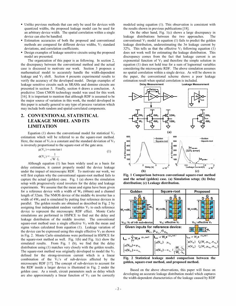
Although equation (1) has been widely used as a basis for delay estimation, it cannot properly model the device leakage under the impact of microscopic RDF. To motivate our work, we will first explain why the conventional square-root method fails to capture the actual (golden) case. Fig. 1 (a) shows the simulation setup with progressively sized inverters for the delay and leakage experiments. We assume that the mean and sigma have been given for a reference device with a width of W0 (60nm) and a channel length of 32nm. The NMOS device of the middle 4x inverter has a width of 4W0 and is simulated by putting four reference devices in parallel. The golden results are obtained as described in Fig. 2 by assigning four independent random variables VT to each reference device to represent the microscopic RDF effect. Monte Carlo simulations are performed in HSPICE to find out the delay and leakage distribution of the middle inverter. The conventional square-root method uses a single effective VT with the mean and sigma values calculated from equation (1). Leakage variation of the device can be expressed using this single effective VT as shown in Fig. 2. Monte Carlo simulations were performed in HSPICE for the square-root method as well. Fig. 1(b) and Fig. 1(c) show the simulated results. From Fig. 1 (b), we find that the delay distribution using (1) matches very closely with the golden results. The square-root method was originally developed to model the VT defined for the strong-inversion current which is a linear combination of the VT’s of sub-devices affected by the microscopic RDF [17]. The concept of sub-devices to account for the RDF inside a larger device is illustrated in Fig. 2 under the golden case. As a result, circuit parameters such as delay which are also approximately a linear function of VT can be correctly
modeled using equation (1). This observation is consistent with the results shown in previous publications [18].
On the other hand, Fig. 1(c) shows a large discrepancy in leakage distributions between the two approaches. The conventional VT model in equation (1) fails to predict the golden leakage distribution, underestimating the 3σ leakage current by 32%. This tells us that the effective VT following equation (1) does not work well for estimating the leakage distribution. This discrepancy comes from the fact that leakage current is an exponential function of VT and therefore the simple solution in equation (1) does not hold true for a sum of lognormal variables considering the microscopic RDF. The above simulation assumes no spatial correlation within a single device. As will be shown in the paper, the conventional scheme shows a poor leakage estimation result when spatial correlation is included.
(a)
(b) (c)
Fig. 1 Comparison between conventional square-root method and the actual (golden) case. (a) Simulation setup; (b) Delay distribution; (c) Leakage distribution.
Fig. 2 Statistical leakage model comparison between the golden, square-root method, and proposed method.
Based on the above observations, this paper will focus on
developing an accurate leakage distribution model which captures the width-dependent characteristics of the leakage caused by RDF
- 3 -
in a nanoscale CMOS device. One assumption used in this paper is that a large device can be considered as a group of smaller devices by ignoring any fringing effect at the device boundary. This is a reasonable assumption for a relatively large device. For minimum width devices where narrow width effect [19] and other fringing effects may not be ignored, our model can be adjusted to account for those situations. For simplicity, we only consider devices with a fixed minimum channel length in this paper. In a real design, the derived model can be easily expanded to a look-up table for handling circuits with multiple channel lengths.
3. PROPOSED STATISTICAL LEAKAGE MODEL The goal of a statistical leakage estimation tool is to obtain an
accurate leakage distribution of a device, circuit block, or full-chip system based on process inputs such as the VT mean and VT sigma of a reference device. Fig. 2 illustrates how the proposed approach is different from the conventional square-root method. Both the proposed and square-root methods introduce an effective VT to represent the device leakage variation using a single variable. However, unlike the square-root method, the mean and sigma of VT in the proposed method is expressed as a function of the device width W as well as the two other inputs (mean and sigma of reference device VT) to match the actual case. The following derivation will show how the actual leakage, which is a sum of lognormal distributions, can be precisely modeled using a single effective VT parameter with a new mean and sigma.
Leakage current of a MOSFET can be expressed as:
T
dsT
VB
)q/kT/(V)q/mkT/(Vleak
We
)e1(WeI⋅−
−−
≅
−∝ (2)
where m is the subthreshold slope coefficient, q is the electron charge, T is the temperature, and k is the Boltzmann’s constant. The term )q/kT/(Vdse− can be ignored as Vds is greater than 3kT/q which is 78mV at room temperature. For simplicity, a constant B is used to represent q/mkT in the following derivation. VT is a Gaussian variable determined by the effective length Leff, dopant concentration Nd, oxide thickness Tox, etc. In this work, we also consider the correlation between the VT of any two devices.
The problem can be now formulated as: Given the mean TxVµ
and sigma TxVσ of VT for a reference device having a width of Wx,
find the mean and sigma value of the effective VT for a device with width Wy that matches the actual (golden) case given in Fig. 2. We will first derive a leakage model assuming an integer multiplicative factor between Wy and Wx, i.e. Wy=nWx. We will later extend the model to a rational number multiplicative factor case in section 3.2.
3.1 Leakage model for discrete width multiplication (Wy=nWx, n: integer)
Let VTy be the effective VT of a device with a width of Wy.
TxVµ and TxVσ are given parameters where VTx is the VT of a
reference device with a width of Wx. The total device leakage can be expressed as:
.eWeW yTiTx VBy
VBn
1ix
⋅−⋅−
=
=∑ (3)
Wy is equal to nWx and iTxV represents the VT of each reference
sub-device considering the microscopic RDF. The mean and sigma of VTy in equation (3) can be expressed using the mean and sigma of VTx using Wilkinson’s method which shows that a sum of
lognormal variables can be approximated to another lognormal variable [20]. For simplicity, we define (µx, σx) as the mean and sigma of the reference device Gaussian variables )VB(
iTx⋅− and
(µy, σy) as those of the total device Gaussian variable )VB( Ty⋅−
in equation (3). We also assume that a correlation coefficient rx between two reference device Gaussian variables )VB(
iTx⋅− is
given to model the spatial correlation. Wilkinson’s method allows us to equate the first moment and second moment of the two lognormal expressions in equation (3) as follows:
2/2/n
1i
2/1
2yy
2xx
2xx nenee)S(Eu σ+µσ+µ
=
σ+µ ==== ∑
2yy
2xx
2x
2xx
2x
2xx
2xx
222r2
n
1ij
2/)r22(21n
1i
n
1i
2222
en))1n(e(ne
)ee2e()S(Eu
σ+µσσσ+µ
+=
σ+σµ−
==
σ+µ
=σ⋅−+=
+== ∑∑∑ (4)
Solving equation (4), we find the following relationship:
∆−σ=σ
∆+µ=µ
2x
2y
xy 21 (5)
where )n
e)1n(eln(
2xx
2x r
2x
σσ ⋅−+−σ=∆ . ∆ is a non-negative
number. By plugging in the constant B, we obtain the following relationship between the VTx and VTy:
22V
2V
VV
B/
B/21
TxTy
TxTy
∆−σ=σ
∆−µ=µ (6)
where )n
e)1n(eln(B2
TxV2
x2
TxV2
Tx
BrB2V
2σσ ⋅−+−σ=∆ .
Equation (6) shows that the mean value of the effective VT is reduced by B/
21 ∆ , which is consistent with our observation in Fig.
1(c) showing that the golden case has a higher average leakage compared to results from the conventional square-root method. The sigma value goes down according to (6) following a similar trend as the square-root method but giving a closer match with the golden case.
Note that the correlation coefficient ry between VTy of two devices is no longer equal to the rx value of the reference device because the device dimensions have changed. An expression for ry is needed to extend the model for the continuous width multiplication case in section 3.2. Hence, we show the derivation of ry in the remainder of this section. Leakage currents of two new devices with equal sizes can be described as:
1yTi1Tx BVy
BVn
1ix eWeW
−−
=
=∑ (7)
2yTi2Tx BVy
BVn
1ix eWeW
−−
=
=∑ .
In order to find the correlation coefficient ry between VTy1 and VTy2, we can equate the correlation coefficient of the left-hand sides to that of the right-hand sides in (7). First of all, the correlation coefficient of the right-hand sides of (7) is:
1e
1e
)eW()eW(
)eW(E)eW(E)eWeW(E
)eW,eW(r
2TyV
2
2TyV
2y
2yT1yT
2yT1yT2yT1yT
2yT1yT
B
Br
BVy
BVy
BVy
BVy
BVy
BVy
BVy
BVy
−
−=
σ⋅σ
⋅−⋅=
σ
σ
−−
−−−−
−−
(8)
- 4 -
Secondly, the correlation coefficient of the left-hand sides of (7) is:
1n
e)1n(e
1e
)eW()eW(
)eW(E)eW(E)eWeW(E
)eW,eW(r
2TxVx
2TxV
2
2TxV
2x
i2Txi1Tx
i2Txi1Txi2Txi1Tx
i2Txi1Tx
rB
Br
BVn
1ix
BVn
1ix
BVn
1ix
BVn
1ix
BVn
1ix
BVn
1ix
BVn
1ix
BVn
1ix
−−+
−=
σ⋅σ
⋅−⋅=
σσ
σ
−
=
−
=
−
=
−
=
−
=
−
=
−
=
−
=
∑∑
∑∑∑∑
∑∑(9)
By equating (8) and (9) and plugging in the relationship between TxVσ and
TyVσ in (6), we find that:
x2V
2V
xBrB
2V
2
y rr
ne)1n(eln
Br
Ty
Tx
2x
2x
2TxV
2Tx ⋅
σσ
=⋅−+
σ=
σσ
(10)
One can also easily prove that 1≥ry≥rx and that ry=1 only when rx=1. Equation (10) shows an interesting observation. As devices become larger, the correlation coefficient between VT of the devices also increases. This is because as dimensions increase, the uncorrelated variation components quickly average out leaving only the correlated variation components to appear in the overall leakage distribution.
3.2 Leakage model for continuous width multiplication (Wy=αWx, α: positive rational number)
Wilkinson’s method cannot be directly applied to solve for the continuous width case: i.e. given TxVµ and TxVσ of VTx for a
device with width Wx, find the TyVµ and TyVσ of VTy for a device with
width Wy where Wy=αWx and α is a positive rational number. To solve this problem, we assume there exists a virtual
reference device with width W0 that satisfies both Wx=mW0 and Wy=nW0. Note that α becomes n/m. 0TVµ , 0TVσ , and r0 denote the mean, standard deviation, and correlation coefficient of VT for the small virtual device. Now we can utilize the results from section 3.1 to carry out our derivation. From equation (6), we have:
2x
2V
2V
xVV
B/
B/21
0TTx
0TTx
∆−σ=σ
∆−µ=µ (11)
where )m
e)1m(eln(B2
0TV2
02
0TV2
0T
BrB2V
2x
σσ ⋅−+−σ=∆ and also:
2y
2V
2V
yVV
B/
B/21
0TTy
0TTy
∆−σ=σ
∆−µ=µ (12)
where )n
e)1n(eln(B2
0TV2
02
0TV2
0T
BrB2V
2y
σσ ⋅−+−σ=∆ .
Solving equations (11) and (12) and applying results from equation (10), we finally find the relationship:
22V
2V
VV
B/
B/21
TxTy
TxTy
∆−σ=σ
∆−µ=µ (13)
where )e)1(e
ln(B2
TxV2
x2
TxV2
Tx
BrB2V
2
α⋅−α+
−σ=∆σσ
. Similarly, we get:
x2V
2V
xBrB
2V
2
y rre)1(eln
Br
Ty
Tx
2x
2x
2TxV
2Tx ⋅
σ
σ=⋅
α−α+
σ=
σσ
(14)
Equations (13) and (14) have the exact same format as equations (6) and (10). This tells us that the same formulas can be applied to both discrete and continuous width cases. Although we started our derivation using a small reference device with a width of Wx, equations (13) and (14) can be used to relate the VT characteristics between any two devices with arbitrary widths, i.e. α can be either larger than 1 or smaller 1. In other word, the derived model can accurately estimate the leakage distribution of an arbitrary width device based on given process inputs for a reference device with any width value. Note that the above derivation is not specific to a certain type of variation. Therefore, the proposed model is general to any process variation sources although RDF is considered as the major cause of variation in this work. The next section will prove the accuracy of the proposed model in (13) and (14).
4. EXPERIMENTAL RESULTS Monte Carlo simulations were performed to compare the
proposed model with the conventional square-root method. The mean and standard deviation values of the reference device were given and multiple reference devices were combined to form a larger device. This setup allows us to verify the leakage distribution for the discrete width multiplication case. Due to the lack of TCAD tools to model the RDF induced VT shift for the continuous width multiplication case, we simply extrapolate the results from the discrete case to a continuous case. Both the theoretical analysis and simulation results exhibit no distinction between the continuous and discrete width multiplication cases.
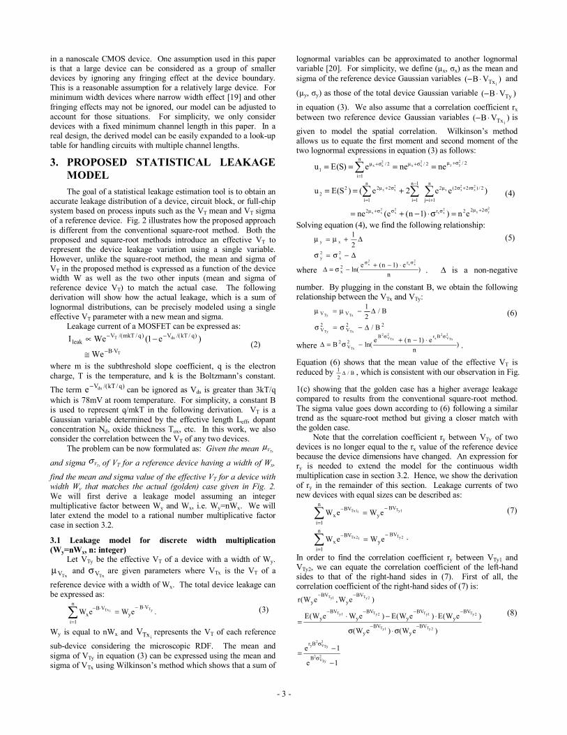
Fig. 3 Statistical leakage estimation results for the golden case, conventional method, and proposed method. (top row: different device widths, middle row: different sigma values, bottom row: different correlation coefficients).
- 5 -
Fig. 3 shows the leakage distribution comparisons for different widths, different VT sigma’s, and different correlation coefficients. The proposed method is compared to the conventional square-root method as well as the golden method. 3σ points on the leakage distributions are marked as a measure of the estimation error. Our proposed method shows a much closer match (less than 5% in most cases) with the golden results while the conventional square-root method exhibits discrepancies as large as 45%. Note that a slightly larger error (12%) is observed for our proposed method when the sigma of the reference device VT is high (Fig. 3, middle right). This stems from the increased error in the Wilkinson’s approximation for Gaussian variables with large standard deviations as mentioned in [20]. Even with this error due to the limitation of Wilkinson’s method, the proposed method still shows a much better fit than the square-root method. Since the intra and inter-die VT variation is normally controlled well below 30%, our model is capable of generating accurate results in a realistic CMOS process.
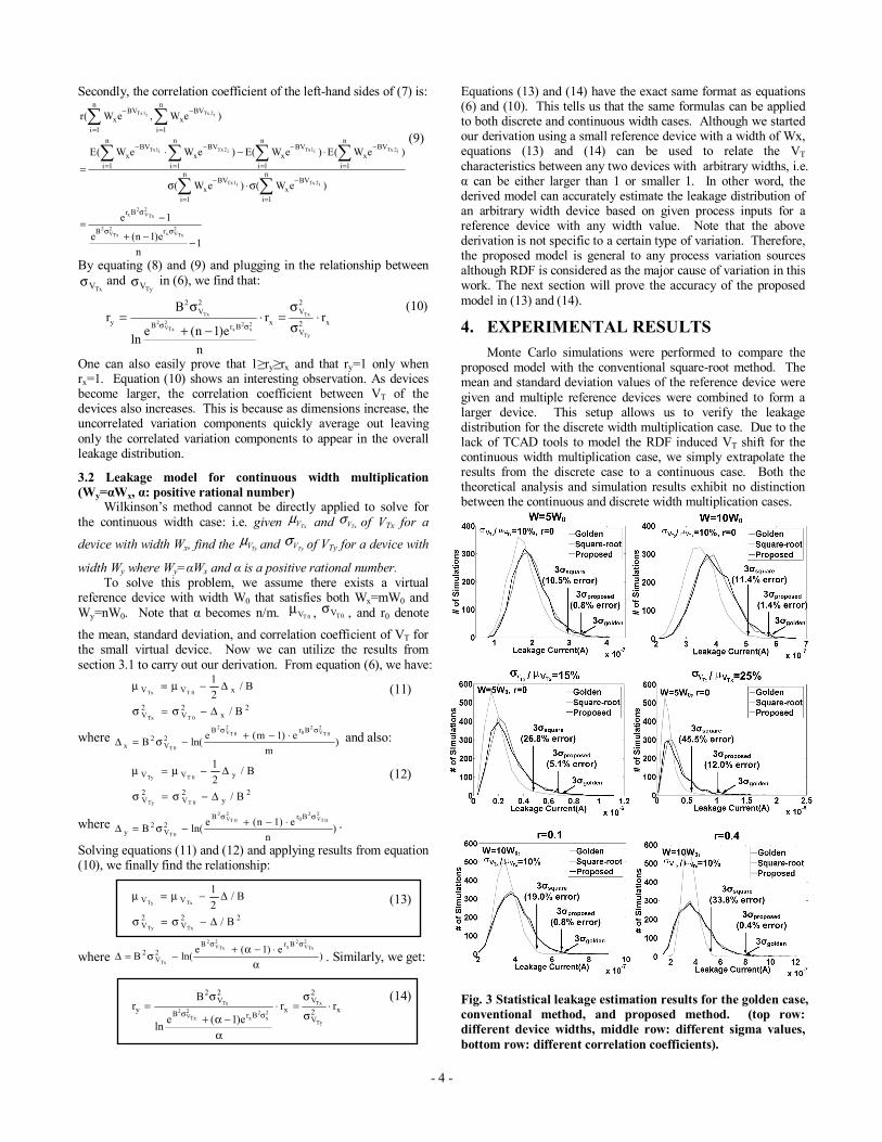
Fig. 4 shows the estimated mean and sigma values of the effective VT for a continuous range of device widths. For larger devices, the mean value of the effective VT estimated by the proposed method is significantly less than that predicted by the square-root method. The difference between the estimated sigma values was less significant. This observation is consistent with what was reported in [11]. Our model summarized in (13) explains the statistical reason behind these physical observations and provides a solution for accurate estimation.
Fig. 4 Estimated mean (top) and standard deviation (bottom) of effective VT versus normalized device width.
5. DESIGNING LEAKAGE SENSITIVE CIRCUITS USING PROPOSED MODEL As mentioned in the introduction, accurate device leakage
modeling is important for estimating the chip power consumption, but is also crucial for optimal design of leakage sensitive circuits such as SRAMs and domino circuits. This section shows design examples using the proposed leakage model for high performance circuits in nanometer CMOS technologies.
5.1 SRAM design: Bitline leakage problem Bitline leakage from unaccessed cells in SRAM bitlines has
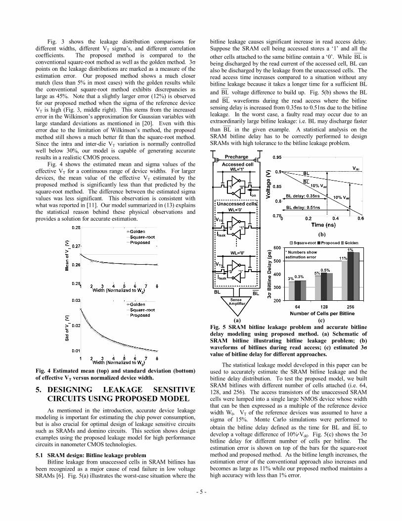
been recognized as a major cause of read failure in low voltage SRAMs [6]. Fig. 5(a) illustrates the worst-case situation where the
bitline leakage causes significant increase in read access delay. Suppose the SRAM cell being accessed stores a ‘1’ and all the other cells attached to the same bitline contain a ‘0’. While BL is being discharged by the read current of the accessed cell, BL can also be discharged by the leakage from the unaccessed cells. The read access time increases compared to a situation without any bitline leakage because it takes a longer time for a sufficient BL and BL voltage difference to build up. Fig. 5(b) shows the BL and BL waveforms during the read access where the bitline sensing delay is increased from 0.35ns to 0.51ns due to the bitline leakage. In the worst case, a faulty read may occur due to an extraordinarily large bitline leakage: i.e. BL may discharge faster than BL in the given example. A statistical analysis on the SRAM bitline delay has to be correctly performed to design SRAMs with high tolerance to the bitline leakage problem.
(a) (c) Fig. 5 SRAM bitline leakage problem and accurate bitline delay modeling using proposed method. (a) Schematic of SRAM bitline illustrating bitline leakage problem; (b) waveforms of bitlines during read access; (c) estimated 3σ value of bitline delay for different approaches.
The statistical leakage model developed in this paper can be used to accurately estimate the SRAM bitline leakage and the bitline delay distribution. To test the proposed model, we built SRAM bitlines with different number of cells attached (i.e. 64, 128, and 256). The access transistors of the unaccessed SRAM cells were lumped into a single large NMOS device whose width that can be then expressed as a multiple of the reference device width W0. VT of the reference devices was assumed to have a sigma of 15%. Monte Carlo simulations were performed to obtain the bitline delay defined as the time for BL and BL to develop a voltage difference of 10%·Vdd. Fig. 5(c) shows the 3σ bitline delay for different number of cells per bitline. The estimation error is shown on top of the bars for the square-root method and proposed method. As the bitline length increases, the estimation error of the conventional approach also increases and becomes as large as 11% while our proposed method maintains a high accuracy with less than 1% error.
(b)
- 6 -
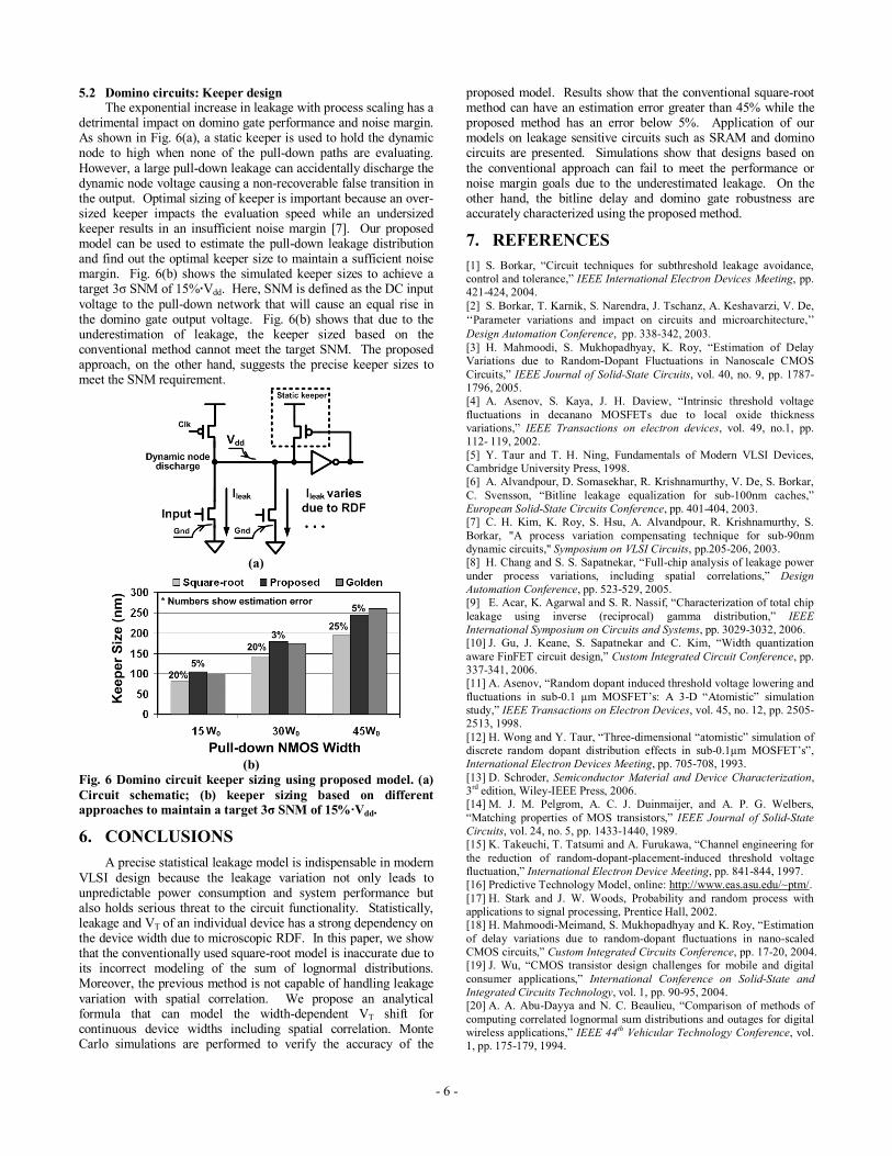
5.2 Domino circuits: Keeper design The exponential increase in leakage with process scaling has a
detrimental impact on domino gate performance and noise margin. As shown in Fig. 6(a), a static keeper is used to hold the dynamic node to high when none of the pull-down paths are evaluating. However, a large pull-down leakage can accidentally discharge the dynamic node voltage causing a non-recoverable false transition in the output. Optimal sizing of keeper is important because an over-sized keeper impacts the evaluation speed while an undersized keeper results in an insufficient noise margin [7]. Our proposed model can be used to estimate the pull-down leakage distribution and find out the optimal keeper size to maintain a sufficient noise margin. Fig. 6(b) shows the simulated keeper sizes to achieve a target 3σ SNM of 15%·Vdd. Here, SNM is defined as the DC input voltage to the pull-down network that will cause an equal rise in the domino gate output voltage. Fig. 6(b) shows that due to the underestimation of leakage, the keeper sized based on the conventional method cannot meet the target SNM. The proposed approach, on the other hand, suggests the precise keeper sizes to meet the SNM requirement.
(a)
(b)
Fig. 6 Domino circuit keeper sizing using proposed model. (a) Circuit schematic; (b) keeper sizing based on different approaches to maintain a target 3σ SNM of 15%·Vdd.
6. CONCLUSIONS A precise statistical leakage model is indispensable in modern
VLSI design because the leakage variation not only leads to unpredictable power consumption and system performance but also holds serious threat to the circuit functionality. Statistically, leakage and VT of an individual device has a strong dependency on the device width due to microscopic RDF. In this paper, we show that the conventionally used square-root model is inaccurate due to its incorrect modeling of the sum of lognormal distributions. Moreover, the previous method is not capable of handling leakage variation with spatial correlation. We propose an analytical formula that can model the width-dependent VT shift for continuous device widths including spatial correlation. Monte Carlo simulations are performed to verify the accuracy of the
proposed model. Results show that the conventional square-root method can have an estimation error greater than 45% while the proposed method has an error below 5%. Application of our models on leakage sensitive circuits such as SRAM and domino circuits are presented. Simulations show that designs based on the conventional approach can fail to meet the performance or noise margin goals due to the underestimated leakage. On the other hand, the bitline delay and domino gate robustness are accurately characterized using the proposed method.
7. REFERENCES [1] S. Borkar, “Circuit techniques for subthreshold leakage avoidance, control and tolerance,” IEEE International Electron Devices Meeting, pp. 421-424, 2004. [2] S. Borkar, T. Karnik, S. Narendra, J. Tschanz, A. Keshavarzi, V. De, ‘‘Parameter variations and impact on circuits and microarchitecture,’’ Design Automation Conference, pp. 338-342, 2003. [3] H. Mahmoodi, S. Mukhopadhyay, K. Roy, “Estimation of Delay Variations due to Random-Dopant Fluctuations in Nanoscale CMOS Circuits,” IEEE Journal of Solid-State Circuits, vol. 40, no. 9, pp. 1787-1796, 2005. [4] A. Asenov, S. Kaya, J. H. Daview, “Intrinsic threshold voltage fluctuations in decanano MOSFETs due to local oxide thickness variations,” IEEE Transactions on electron devices, vol. 49, no.1, pp. 112- 119, 2002. [5] Y. Taur and T. H. Ning, Fundamentals of Modern VLSI Devices, Cambridge University Press, 1998. [6] A. Alvandpour, D. Somasekhar, R. Krishnamurthy, V. De, S. Borkar, C. Svensson, “Bitline leakage equalization for sub-100nm caches,” European Solid-State Circuits Conference, pp. 401-404, 2003. [7] C. H. Kim, K. Roy, S. Hsu, A. Alvandpour, R. Krishnamurthy, S. Borkar, "A process variation compensating technique for sub-90nm dynamic circuits," Symposium on VLSI Circuits, pp.205-206, 2003. [8] H. Chang and S. S. Sapatnekar, “Full-chip analysis of leakage power under process variations, including spatial correlations,” Design Automation Conference, pp. 523-529, 2005. [9] E. Acar, K. Agarwal and S. R. Nassif, “Characterization of total chip leakage using inverse (reciprocal) gamma distribution,” IEEE International Symposium on Circuits and Systems, pp. 3029-3032, 2006. [10] J. Gu, J. Keane, S. Sapatnekar and C. Kim, “Width quantization aware FinFET circuit design,” Custom Integrated Circuit Conference, pp. 337-341, 2006. [11] A. Asenov, “Random dopant induced threshold voltage lowering and fluctuations in sub-0.1 µm MOSFET’s: A 3-D “Atomistic” simulation study,” IEEE Transactions on Electron Devices, vol. 45, no. 12, pp. 2505-2513, 1998. [12] H. Wong and Y. Taur, “Three-dimensional “atomistic” simulation of discrete random dopant distribution effects in sub-0.1µm MOSFET’s”, International Electron Devices Meeting, pp. 705-708, 1993. [13] D. Schroder, Semiconductor Material and Device Characterization, 3rd edition, Wiley-IEEE Press, 2006. [14] M. J. M. Pelgrom, A. C. J. Duinmaijer, and A. P. G. Welbers, “Matching properties of MOS transistors,” IEEE Journal of Solid-State Circuits, vol. 24, no. 5, pp. 1433-1440, 1989. [15] K. Takeuchi, T. Tatsumi and A. Furukawa, “Channel engineering for the reduction of random-dopant-placement-induced threshold voltage fluctuation,” International Electron Device Meeting, pp. 841-844, 1997. [16] Predictive Technology Model, online: http://www.eas.asu.edu/~ptm/. [17] H. Stark and J. W. Woods, Probability and random process with applications to signal processing, Prentice Hall, 2002. [18] H. Mahmoodi-Meimand, S. Mukhopadhyay and K. Roy, “Estimation of delay variations due to random-dopant fluctuations in nano-scaled CMOS circuits,” Custom Integrated Circuits Conference, pp. 17-20, 2004. [19] J. Wu, “CMOS transistor design challenges for mobile and digital consumer applications,” International Conference on Solid-State and Integrated Circuits Technology, vol. 1, pp. 90-95, 2004. [20] A. A. Abu-Dayya and N. C. Beaulieu, “Comparison of methods of computing correlated lognormal sum distributions and outages for digital wireless applications,” IEEE 44th Vehicular Technology Conference, vol. 1, pp. 175-179, 1994.