Embed Size (px)
DESCRIPTION
basics of electronics
Citation preview
S.KAL, IIT - KHARAGPUR
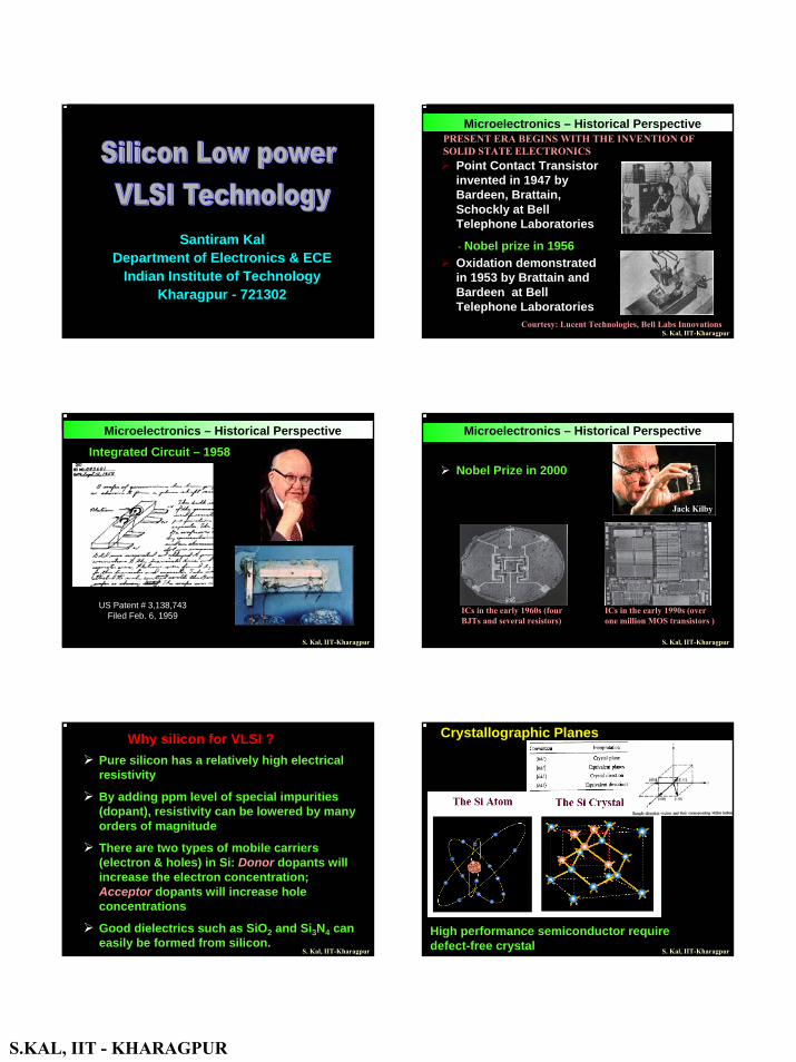
Santiram KalDepartment of Electronics & ECE
Indian Institute of TechnologyKharagpur - 721302
PRESENT ERA BEGINS WITH THE INVENTION OF SOLID STATE ELECTRONICS
Microelectronics – Historical Perspective
Point Contact Transistor invented in 1947 by Bardeen, Brattain, Schockly at Bell Telephone Laboratories
- Nobel prize in 1956Oxidation demonstrated in 1953 by Brattain and Bardeen at Bell Telephone Laboratories
Courtesy: Lucent Technologies, Bell Labs InnovationsS. Kal, IIT-Kharagpur
US Patent # 3,138,743 Filed Feb. 6, 1959
Integrated Circuit – 1958
Microelectronics – Historical Perspective
S. Kal, IIT-Kharagpur
Microelectronics – Historical Perspective
Nobel Prize in 2000
Jack Kilby
ICs in the early 1960s (four BJTs and several resistors)
ICs in the early 1990s (over one million MOS transistors )
S. Kal, IIT-Kharagpur
Pure silicon has a relatively high electrical resistivity
By adding ppm level of special impurities (dopant), resistivity can be lowered by many orders of magnitude
There are two types of mobile carriers (electron & holes) in Si: Donor dopants will increase the electron concentration; Acceptor dopants will increase hole concentrations
Good dielectrics such as SiO2 and Si3N4 can easily be formed from silicon.
Why silicon for VLSI ?
S. Kal, IIT-Kharagpur
High performance semiconductor require defect-free crystal
Crystallographic Planes
S. Kal, IIT-Kharagpur
S.KAL, IIT - KHARAGPUR
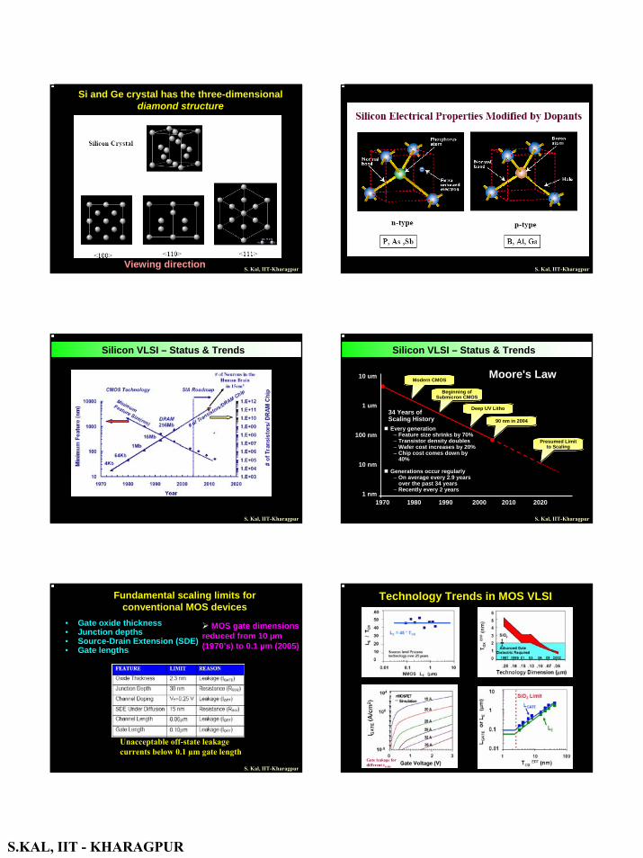
Viewing direction
Si and Ge crystal has the three-dimensional diamond structure
S. Kal, IIT-Kharagpur S. Kal, IIT-Kharagpur
Technology Trends in VLSI Silicon VLSI – Status & Trends
S. Kal, IIT-Kharagpur
Technology Trends in VLSI
Modern CMOSModern CMOS
Beginning ofSubmicron CMOS
Beginning ofSubmicron CMOS
Deep UV LithoDeep UV Litho
90 nm in 200490 nm in 2004
Presumed Limitto Scaling
Presumed Limitto Scaling
Moore's Law10 um
1 um
100 nm
10 nm
1 nm1970 1980 1990 2000 2010 2020
34 Years of Scaling HistoryEvery generation
– Feature size shrinks by 70%– Transistor density doubles– Wafer cost increases by 20%– Chip cost comes down by
40%
Generations occur regularly– On average every 2.9 years
over the past 34 years– Recently every 2 years
Silicon VLSI – Status & Trends
S. Kal, IIT-Kharagpur
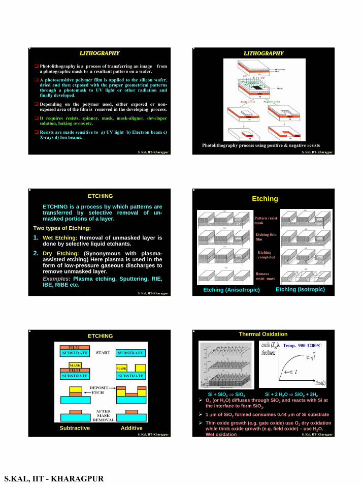
Fundamental scaling limits for conventional MOS devices
• Gate oxide thickness• Junction depths• Source-Drain Extension (SDE)• Gate lengths
MOS gate dimensions reduced from 10 µm (1970’s) to 0.1 µm (2005)
Unacceptable off-state leakage currents below 0.1 µm gate length
S. Kal, IIT-Kharagpur
Technology Trends in MOS VLSI
Gate leakage for different toxide

S.KAL, IIT - KHARAGPUR
Technology Trends in MOS VLSI
Active and standby power trends
Chip power and frequency trends
Off-state leakage vs L for 0.25 transistor with different Vth
Power supply and threshold voltage scaling trends
Power Management in VLSI TechnologyTotal chip power dissipation (P) = Dynamic power dissipation (Pdyn) + Static power dissipation (Pstat)
clockddactivedyn fVCP 2= leakddoffStatic IVWNP =
onddgi
i IVCf
/1==τ
Vdd = power supply voltage
Cactive = total capacitance being switched during an average clock cycleFclock = chip clock frequency
Noff = No. of transistors that do not switch during an average clock cycle.W = average transistor widthIleak = total transistor leakage current ( A/ µm of transistor width)
τi = transistor intrinsic delay
fi = transistor intrinsic frequencyCg = gate capacitance per micron of transistor width for a MOSFET of gate length Lg
Ion = transistor saturation drive current, which must be maximized to maximize fi
S. Kal, IIT-Kharagpur
High Performance Technology Requirement Table
Year Units 2003 2006 2009 2012 2015 2018
Lgate nm 45 28 20 14 10 7
EOT A 13 10 8 7 6 5
Vdd V 1.2 1.1 1.0 0.9 0.8 0.7
Vth V 0.21 0.21 0.16 0.14 0.12 0.11
Parasitic(RSD)
Ohm µm
180 171 144 116 88 60
Cg F/µm 7.4E-16 5.7E-16 5.8E-16 4.4E-16 3.5E-16 2.7E-16
Cpara F/µm 2.4E-16 2.3E-16 1.9E-16 1.5E-16 1.2E-16 8.0E-17
Psatic W/µm 4.0E-07 6.1E-07 7.7E-07 9.9E-07 2.6E-06 3.9E-06
tD
(NAND)
pS 30.24 18.92 12.06 7.47 4.45 2.81
(Data from 2003 ITRS)
Equivalent Oxide Thickness (EOT) = Td / ( K/Kox) ; using high-K dielectric of thickness Td and relative dielectric constant K. Kox = 3.9 (SiO2)
Low Power VLSI Technology
Major Issues……..• Reduction of power supply
• Reduction of device leakage currents
• Reduction of parasitic resistances and capacitances
Active power is set by circuit switching, P = CLoad Vcc2 f
( f is operating freq. and CLoad is the switching capacitance of the gate and wire load )
Standby power results from junction and transistor sub-threshold source-to-drain leakage
S. Kal, IIT-Kharagpur
Low Power VLSI Technology
Solutions……..• Use of proper isolation scheme to reduce
parasitics
• SOI Technologies
• Complementary transistor structures
• BiCMOS Technologies
S. Kal, IIT-Kharagpur
The fabrication process sequence of an Integrated Circuit
S. Kal, IIT-Kharagpur
S.KAL, IIT - KHARAGPUR
Crystal Growth
S. Kal, IIT-Kharagpur
VLSI Technology :Unit Processes• Wafer Cleaning• Oxidation• Lithography• Etching• Diffusion• Ion-implantation• Epitaxy• Deposition of thin films• Metallization• Bonding & Packaging
S. Kal, IIT-Kharagpur
Killing Defects and Contaminations in VLSI
Wafer Cleaning & Clean Room Contaminants
S. Kal, IIT-Kharagpur
Impact of Defects
S. Kal, IIT-Kharagpur
Impact of Contaminants on Device ParametersParameters Hydro-
Carbons,O2, N2
Alkali metals Heavy metals
Dopants Particulates
MOS drive currents
X X X
Threshold, Flatband
X X X
Oxide leakage X X XMinority life time
X X X
Diode leakage X X X XJunction break-down
X X X X
Bipolar gain X XCrystal defects X X XInter- connect open/short
X X
DEFECTS & CONTAMINATIONS
S. Kal, IIT-Kharagpur
Clean Room Performance ( Yellow Room )
1. Cleanliness class → Process area ≤ 10→ Service area ≤ 1000
2. Temperature → 22 ± 0.5 º C
3. Humidity → 43 ± 5 %
4. Air quality → NO2 < 0.5 ppb→ SO2 < 0.5 ppb→ Hydrocarbon < 100 ppb
DEFECTS & CONTAMINATIONS
S. Kal, IIT-Kharagpur
S.KAL, IIT - KHARAGPUR
Photolithography is a process of transferring an image from a photographic mask to a resultant pattern on a wafer.
A photosensitive polymer film is applied to the silicon wafer, dried and then exposed with the proper geometrical patterns through a photomask to UV light or other radiation and finally developed.
Depending on the polymer used, either exposed or non-exposed area of the film is removed in the developing process.
It requires resists, spinner, mask, mask-aligner, developer solution, baking ovens etc.
Resists are made sensitive to a) UV light b) Electron beam c) X-rays d) Ion beams.
S.KAL, IIT- KHARAGPUR
LITHOGRAPHY LITHOGRAPHY
S. Kal, IIT-Kharagpur
Photolithography process using positive & negative resistsS.KAL, IIT- KHARAGPUR
LITHOGRAPHY LITHOGRAPHY
S. Kal, IIT-Kharagpur
ETCHING is a process by which patterns are transferred by selective removal of un-masked portions of a layer.
Two types of Etching:
1. Wet Etching: Removal of unmasked layer is done by selective liquid etchants.
2. Dry Etching: (Synonymous with plasma-assisted etching) Here plasma is used in the form of low-pressure gaseous discharges to remove unmasked layer.Examples: Plasma etching, Sputtering, RIE, IBE, RIBE etc.
ETCHING
S. Kal, IIT-Kharagpur
Etching
Etching (Anisotropic) Etching (Isotropic)
Pattern resist mask
Etching thin film
Etching completed
Remove resist mask
Subtractive Additive
ETCHING
S. Kal, IIT-Kharagpur
Thermal Oxidation
Si + SiO2 ⇒ SiO2 Si + 2 H2O⇒ SiO2 + 2H2O2 (or H2O) diffuses through SiO2 and reacts with Si at the interface to form SiO2.
1 μm of SiO2 formed consumes 0.44 μm of Si substrate
Thin oxide growth (e.g. gate oxide) use O2 dry oxidation while thick oxide growth (e.g. field oxide) – use H2O. Wet oxidation
Temp. 900-1200oC
S. Kal, IIT-Kharagpur

S.KAL, IIT - KHARAGPUR
Uneven surface topography with window oxidation
S. Kal, IIT-Kharagpur
Local Oxidation (LOCOS)
Note surface topography
S. Kal, IIT-Kharagpur
ION IMPLANTATION
Ion implantation is a process of introduction of ionized projectile atoms (impurity) in to targets (Si-substrates) with enough energy to penetrate beyond surface region of a single crystal substrate in order to change its electronic properties.
Dopant atoms are vaporized, accelerated and directed at silicon substrate.
Dopants enter the crystal lattice, collide with silicon atoms, gradually lose energy, finally coming to rest at some depth within the lattice
S. Kal, IIT-Kharagpur
Ion ImplantationTypically used to introduce dopants in to semiconductor
S. Kal, IIT-Kharagpur
Thermal Diffusion
To introduce dopantsinto semiconductor (Predeposition)
To spread out the dopant profile ( Drive-in)
S. Kal, IIT-Kharagpur
Predeposition + Drive-in
Half-Gaussian profile after long drive-in
Dopant dose conservedduring drive-in
Diffusion distance,
Dt≅
S. Kal, IIT-Kharagpur

S.KAL, IIT - KHARAGPUR
In present VLSI process pre-deposition diffusion is totally replaced by ion implantation. Why?
a. Control of doping Excellent Good profile 0
b. Shallow junction Min. 100 A Noc. Max. doping > Solid solubility Solubility limitd. Control parameter Electrical Thermodynamic
(Ion energy,dose, ( Temp, time )ion current)
e. Elec. conductivity Poor (requires Goodannealing)
f. Damages High (requires Lowannealing)
ION IMPLANTATION
Implant Pre-depositiondiffusion
S. Kal, IIT-Kharagpur
Physical vapor deposition(Evaporation deposition)
S. Kal, IIT-Kharagpur
Physical vapor deposition(Sputtering deposition)
S. Kal, IIT-Kharagpur
Chemical vapor deposition
Solid films are formed by chemical reaction taking place at the surface
S. Kal, IIT-Kharagpur
EpitaxyEpitaxy ( “epi” → upon + “taxis” → ordered ) is the ordered growth of thin single crystal layer upon a crystalline substratePurity and crystal quality of epi-layer is better than in substrateSilicon epitaxy is used for bipolar devices and in CMOS –latch up prevention
Widely employed in compound semiconductor materialsBipolar IC application (1 – 3 μm in high speed digital circuits and 3 – 10 μm in linear circuits)
EPITAXY
S. Kal, IIT-Kharagpur
Epitaxial Growth
Processing temperature 950 – 1050 deg CRequire an ultra-clean Si surface prior to epigrowthRequire deposition of Si at very high temperature for perfect crystallinity
S. Kal, IIT-Kharagpur

S.KAL, IIT - KHARAGPUR
Vapor Phase Epitaxy reactor system
EPITAXY
S. Kal, IIT-Kharagpur
Molecular Beam Epitaxy
Features :Non – CVD vapor phase epitaxy via evapo-ration of material in ultra – high vacuum environment. By utilizing very low growth rates ( ≈ 1 μm/hour) can tailor doping profiles and composition on a monolayer scale.
Growth temperature 400o – 800oCBackground vacuum pressures ≈ 10-11 TorrUsed for growth of Silicon, GaAs, AlGaAs, II –VI materials
EPITAXY
S. Kal, IIT-Kharagpur
MBE Reactor Configuration
EPITAXY
S. Kal, IIT-Kharagpur
Device Isolation Methods
S. Kal, IIT-Kharagpur
This method makes use of the fact that a reverse biased p – n junction has extremely low leakage current. Two regions on a semiconductor substrate are effectively isolated by applying a suitable reverse bias
Junction / Diode Isolation
Junction isolation suffers from low breakdown voltage and unwanted parasitic capacitances which prevent it to be used for high frequency application
ISOLATION TECHNOLOGY 6
S. Kal, IIT-Kharagpur

S.KAL, IIT - KHARAGPUR
Complete Dielectric IsolationThis isolation scheme produces several pockets on a single crystal substrate surrounded by thin dielectric layers
ISOLATION TECHNOLOGY
This scheme is specially suitable for high voltage applications and for nuclear-radiation environments
S.KAL, IIT- KHARAGPURS. Kal, IIT-Kharagpur
Oxide IsolationThis is basically a junction – dielectric isolation where p-n junction isolation is combined with isolation produced by local oxidation of siliconThis scheme produces isolated silicon islands, whose boarders are defined by a frame of locally thermally grown SiO2 that completely or partially penetrates the epitaxial layer.This technique has resulted in great reduction in the physical dimension of the devices making it suitable for VLSI circuits.
ISOLATION TECHNOLOGY
S.KAL, IIT- KHARAGPURS. Kal, IIT-Kharagpur
LOCal Oxidation of Silicon (LOCOS) IsolationLOCOS has now become the standard isolation scheme in VLSI. It addresses both the isolation and parasitic device formation.
ISOLATION TECHNOLOGY
S.KAL, IIT- KHARAGPUR
Formation of defects (dislocation) in silicon because of stress; Si3N4 causes Kooi effect or white ribbon effect i.e., it inhibits subsequent oxidation due to nitride patches
Pad oxide is used ⇒ get Bird’s Head, Bird’s BeakS. Kal, IIT-Kharagpur
LOCOSSince oxidation consumes 44% as much silicon as it grows, the resultant oxide is partially recessed and has a gradual step on to the field that forms Bird’s Head.
Oxide encroachment in active area produces Bird’s Beak
If the silicon is etched first, the field oxide can be made fullyrecessed, resulting a nearly planner surface.
Although recessed silicon with pad oxide offers isoplanar surface and reduces Bird’s Head, Bird’s Beak still remains.
ISOLATION TECHNOLOGY
S. Kal, IIT-Kharagpur
Side Wall Masked Isolation ( SWAMI) ProcessImportant consequence of Bird’s Beak from device standpoint are ——
o Encroachment reduces the active width of the device, reducing the amount of current that a transistor will drive
o Field doping may increase the threshold voltage reducing its drive current – known as narrow channel effect.
ISOLATION TECHNOLOGY
SWAMI process reduces real estate waste. It redu-ces Bird’s Beak length
S. Kal, IIT-Kharagpur
Silicon on Insulator (SOI) Isolation Encasing of each device in an insulating material is an ideal method of device isolation. Generically they are called Silicon on Insulator (SOI)
SOI devices suffer from problems related to defect density. For that reason Si SOI technologies occupied small market such as radiation hardened devices
One of the most promising SOI technique discussed earlier is SIMOX, where a buried oxide is formed by implanting the wafer with 150 to 300 keV O+ at doses of about 2 X 1018 cm -2
One of the first SOI methods, called dielectric isolation (DI). DI was developed to build high voltage telecomm-unication ICs that required electrically isolated bi-directional switches
ISOLATION TECHNOLOGY
S.KAL, IIT- KHARAGPURS. Kal, IIT-Kharagpur
S.KAL, IIT - KHARAGPUR
Silicon on Insulator Isolation Technique
Deep grooves are first etched in the surface of the wafer
The wafer is oxidized and a very thick ( > 200 μm) poly-Si is deposited by conventional CVD
The wafer is turned over and mechanically ground until the grooves penetrate through the wafer
Finally the wafer is chemically polished and devices are fabricated in the isolated islands
Problems are planarity, high cost, small isolation density
ISOLATION TECHNOLOGY
S.KAL, IIT- KHARAGPURS. Kal, IIT-Kharagpur
Contacts to Silicon
S. Kal, IIT-Kharagpur
Contacts to Silicon
S. Kal, IIT-Kharagpur
Resistance and Sheet Resistance
Sheet Resistance (in ohms/square)
RS = ρ /t
when W = L
R = RS L / W
S. Kal, IIT-Kharagpur
BASE DIFFUESD RESISTOR
RESISTOR GEOMETRIES
RESISTOR CROSS SECTION
S. Kal, IIT-Kharagpur

S.KAL, IIT - KHARAGPUR
CROSS SECTION SCHEMATIC OF AN INTEGRATED NPN TRANSISTOR
I. ISOLATION
II. DEEP
COLLECTOR
III. EXTRINSIC
COLLECTOR
IV. INTRINSIC
BASE
V. EXTRINSIC
BASE
S. Kal, IIT-Kharagpur
CONCENTRATION PROFILE (INTRINSIC REGION)
OF N-P-N TRANSISTOR
EPITAXY: 5.2 μm, P, 5×10¹⁵/cc
BURIED LAYER: SB,
80 Kev, 1.5 × 1015 cm –2
EMITTER JUNCTION: 1.08 μm
BASE JUNCTION: 1.78 μm
EPI / SUB JUNCTION: 9.42 μm
BASE WIDTH = 0.7 μm
NET EPI WIDTH = 1.12 μm
S. Kal, IIT-Kharagpur
Progress of transistor geometries from Planar to the Isoplanar II
S. Kal, IIT-Kharagpur
Process flow for an oxide isolated triple diffused bipolar technology
BIPOLAR PROCESS TECHNOLOGY 9
S. Kal, IIT-Kharagpur
BIPOLAR PROCESS TECHNOLOGY
Process flow for an oxide isolated triple diffused bipolar technology
S. Kal, IIT-Kharagpur
BIPOLAR PROCESS TECHNOLOGY
Process flow for an oxide isolated triple diffused bipolar technology
Steps include:(a) buried layer formation, (b) epitaxialgrowth, (c) LOCOS patterning, (d) silicon recessing and channel stop implants, (e) local oxidation, (f) intrinsic base implant, (g) contact growth, (h) extrinsic base implant, (i) emitter and collector contact implant, and (j) metallization.
11
S. Kal, IIT-Kharagpur

S.KAL, IIT - KHARAGPUR
Process flow for a self aligned double poly bipolar tech.After buried collector and isolation formation, a p+
layer of polysilicon is deposited. This layer is doped in-situ during depositionA layer of oxide is then deposited or grown on the p+ polyThe first poly is then patterned to open window in an active region
BIPOLAR PROCESS TECHNOLOGY 24
The extrinsic base is diffused out of the first poly
S. Kal, IIT-Kharagpur
A second oxide is deposited or grown and reactive ion etched back down to substrate, leaving sidewall spacers on the base contactsThe intrinsic base is implanted through the holeThe second poly is deposited, doped n-type, and the emitter is drivenFinally some of the base and emitter areas may be silicided to reduce series resistance
BIPOLAR PROCESS TECHNOLOGYProcess flow for a self aligned double poly bipolar tech.
Base and emitter contacts align themselves automatically due to the surface topology without the need for a critical alignment step
25
S. Kal, IIT-Kharagpur
BIPOLAR PROCESS TECHNOLOGY
Sidewall Base Contact Structure ( SICOS) Transistor31
1. An n– collector is selec-tively grown epitaxially in the window and p-silicon is formed epitaxially
2. Base contacts are diffused laterally from the p+ poly
3. After oxide patterning, n+
poly is deposited and n+
poly contact emitter is formed
Although many reports of SICOS have appeared, it is yet to be used in any mainstream process because of higher defects and leakage during selective epi growth
S. Kal, IIT-Kharagpur
Salicide NMOS Process Sequence
After LOCOS process, thin gate oxide is formed. Poly – Si deposited and patterned. Source/ Drain implanted
Formation of sidewall oxide spacers – the spacers is formed by depositing oxide layer about 200 nm thick and etching it with anisotropic RIE. All the oxide in the field will be cleared except at regions next to sharp steps where deposited oxide is thickest.
MOS PROCESS TECHNOLOGY 9
S. Kal, IIT-Kharagpur
Metal (Ti, Co) is deposited then annealed using RTP. Metal film is allowed to react with exposed active regions of the devices and silicides are formed over gate and S/D contacts. Un-reacted metal is removed selectively
It is found that Ti thickness showed to be one fifth of the original junction depth in order to avoid excessive leakage current
MOS PROCESS TECHNOLOGY
Salicide NMOS Process Sequence
10
S. Kal, IIT-Kharagpur

S.KAL, IIT - KHARAGPUR
→Although TiSi2 is highly popular in SALICIDE process MoSi2 may be a better choice for NMOS application because of its lower barrier height (0.55 eV) which provides a lower sp. contact resistance
MOS PROCESS TECHNOLOGY
Salicide NMOS Process Sequence Glass passivation layer is deposited, contacts are formed and metallization follows
The use of salicide process can significantly reduce the parasitic series resistance of the MOSFET
11
S. Kal, IIT-Kharagpur
Hot Carrier Effects in Short-Channel MOS• In the reverse-bias drain-to-substrate junction, the electric field
may be quite high in the short-channel devices
• Carriers that are injected into the depletion layer are accelerated by the high field, and some of them may gain enough energy to cause impact ionization. These carriers have higher energy than the thermal energy and are called hot carriers
• Holes – may terminate to substrate giving Isubs, may find their way to source lowering the source barrier to induce electron injection
• Drain-channel-source structure now acts as npn transistor with floating base and collector under avalance multiplication
• The electrons may be attracted to +ve gate and may tunnel into oxide to produce gate current. Trapped electrons in gate oxide may change Vt
MOS PROCESS TECHNOLOGY 12
S. Kal, IIT-Kharagpur
Drain Engineering in MOS Lightly Doped Drain (LDD) structure
Hot carrier effects are alleviated by LDD structure which reduces the drain field
In LDD structure, the drain is formed by two implants, one of these is self-aligned to the gate electrode and the other is self-aligned to an oxide spacer at the edge of the gate
Lateral dimension of oxide spacer ≈ 75 % of oxide thickness. In nMOS ; lighter drain → P, 10-13 cm-2
dose and higher doped region → As, 10-15 cm-2 dose, LS ≈ 160 nm ≈ 0.16 μm
Thus electric field is reduced to an acceptable level near the gate edge because of lighter drain.
MOS PROCESS TECHNOLOGY 13
S. Kal, IIT-Kharagpur
Formation of oxide sidewall spacers
Source/ drain implant
Silicide contact forma-tion and metallization
However, LDD structure adds additional parasi-tic resistance
MOS PROCESS TECHNOLOGYLightly Doped Drain (LDD) MOS Process
An optimization process for the reachthrough doping, depth and length must be carried out in which the tra-nsistor performance must be balanced against device reliability
17
S. Kal, IIT-Kharagpur
BiCMOS is a technology that integrates both CMOS and bipolar device structures on the same chip
CMOS can offer low power and high density to a digital IC, but it is usually slower than the emitter-coupled logic (ECL)-based ICs
Bipolar transistors, on the other hand, can deliver large drive currents, operate with small logic swings, and have high noise immunity; however, they exhibit high power consumption, poor density, and limited circuit options.
BiCMOS offer the benefits of both bipolar and CMOS circuits
By appropriate trading off the characteristics of each technology, speed and power can be balanced
This desirable result, however, is attained with the penalty of adding more process complexity
BiCMOS TECHNOLOGY
S. Kal, IIT-Kharagpur
Standard Buried Collector (SBC) BiCMOS Process
SBC BiCMOS process uses a buried n+ layer under the n-well
Buried n+ layer is first formed in p-substrate by arsenic implant and capped with 2 μm thick n-epi layer
3D BiCMOS suffers from high collector resistance due to use of lightly doped n-well as collector
BiCMOS TECHNOLOGY
S. Kal, IIT-Kharagpur
S.KAL, IIT - KHARAGPUR
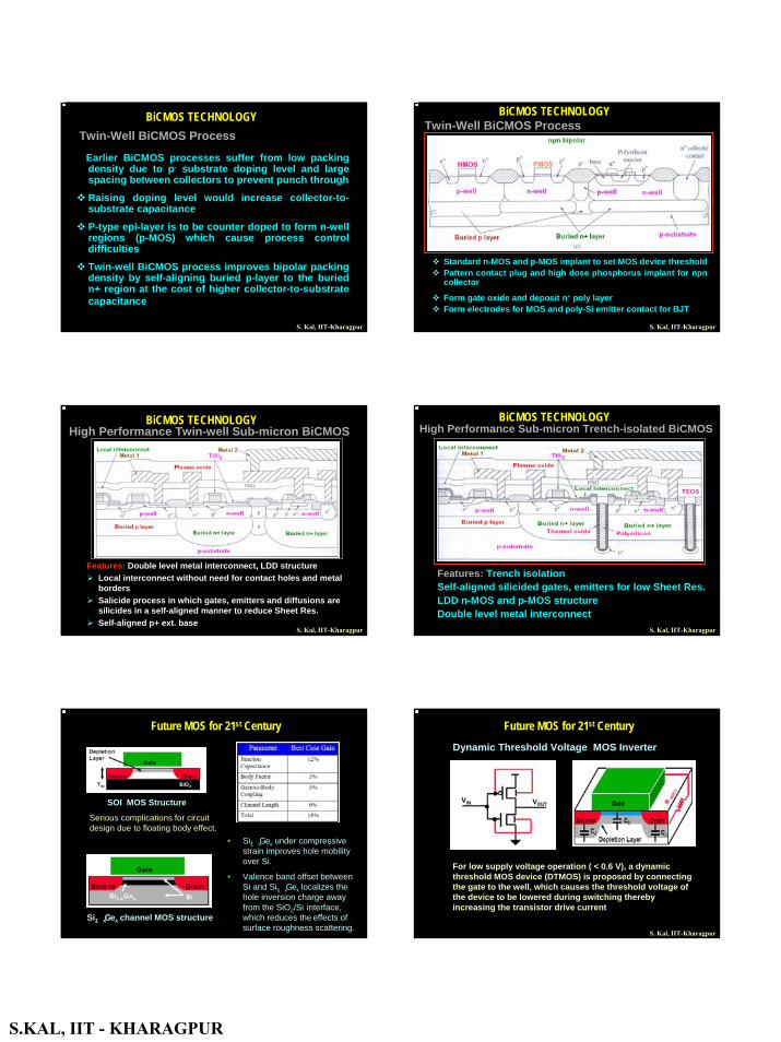
Twin-Well BiCMOS Process
Earlier BiCMOS processes suffer from low packing density due to p- substrate doping level and large spacing between collectors to prevent punch through
Raising doping level would increase collector-to-substrate capacitance
P-type epi-layer is to be counter doped to form n-well regions (p-MOS) which cause process control difficulties
Twin-well BiCMOS process improves bipolar packing density by self-aligning buried p-layer to the buried n+ region at the cost of higher collector-to-substrate capacitance
BiCMOS TECHNOLOGY
S. Kal, IIT-Kharagpur
Twin-Well BiCMOS Process
Standard n-MOS and p-MOS implant to set MOS device thresholdPattern contact plug and high dose phosphorus implant for npncollector
Form gate oxide and deposit n+ poly layerForm electrodes for MOS and poly-Si emitter contact for BJT
BiCMOS TECHNOLOGY
S. Kal, IIT-Kharagpur
High Performance Twin-well Sub-micron BiCMOS
Features: Double level metal interconnect, LDD structureLocal interconnect without need for contact holes and metal bordersSalicide process in which gates, emitters and diffusions are silicides in a self-aligned manner to reduce Sheet Res.Self-aligned p+ ext. base
BiCMOS TECHNOLOGY
S. Kal, IIT-Kharagpur
High Performance Sub-micron Trench-isolated BiCMOS
Features: Trench isolationSelf-aligned silicided gates, emitters for low Sheet Res.LDD n-MOS and p-MOS structureDouble level metal interconnect
BiCMOS TECHNOLOGY
S. Kal, IIT-Kharagpur
Future MOS for 21st Century
SOI MOS Structure
Si1- xGex channel MOS structure
• Si1- xGex under compressive strain improves hole mobility over Si.
• Valence band offset between Si and Si1- xGex localizes the hole inversion charge away from the SiO2/Si interface, which reduces the effects of surface roughness scattering.
Serious complications for circuit design due to floating body effect.
Future MOS for 21st CenturyDynamic Threshold Voltage MOS Inverter
For low supply voltage operation ( < 0.6 V), a dynamic threshold MOS device (DTMOS) is proposed by connecting the gate to the well, which causes the threshold voltage of the device to be lowered during switching thereby increasing the transistor drive current
S. Kal, IIT-Kharagpur
S.KAL, IIT - KHARAGPUR
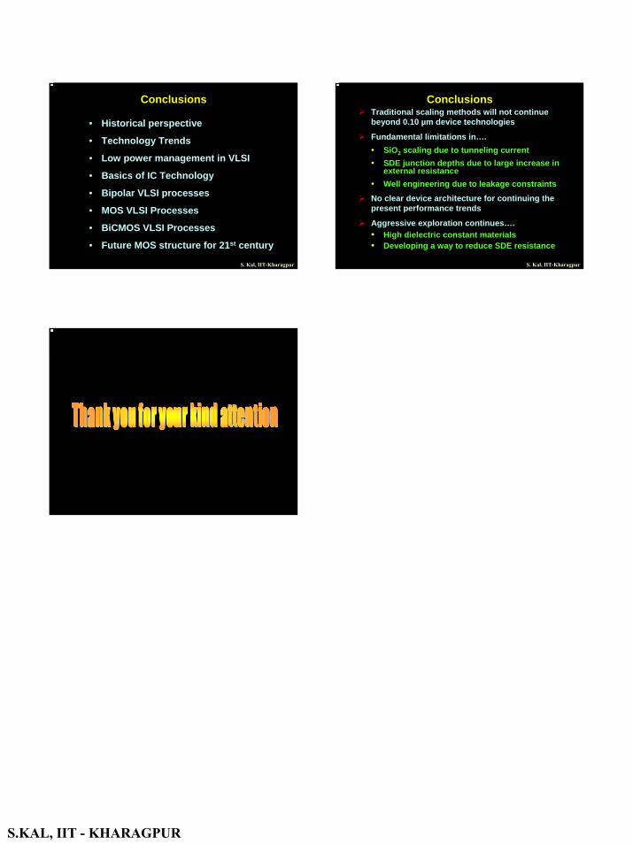
Conclusions
• Historical perspective
• Technology Trends
• Low power management in VLSI
• Basics of IC Technology
• Bipolar VLSI processes
• MOS VLSI Processes
• BiCMOS VLSI Processes
• Future MOS structure for 21st century
S. Kal, IIT-Kharagpur
ConclusionsTraditional scaling methods will not continue beyond 0.10 µm device technologies
Fundamental limitations in….• SiO2 scaling due to tunneling current• SDE junction depths due to large increase in
external resistance• Well engineering due to leakage constraints
No clear device architecture for continuing the present performance trends
Aggressive exploration continues….• High dielectric constant materials• Developing a way to reduce SDE resistance
S. Kal, IIT-Kharagpur