Embed Size (px)
Citation preview

FEATURES APPLICATIONS
DESCRIPTION
DAC8830-EPDAC8831-EP
SGLS334C–AUGUST 2006–REVISED APRIL 2007
16-Bit, Ultra-Low Power, Voltage-OutputDigital-to-Analog Converters
• Portable Equipment• Controlled Baseline• Automatic Test Equipment– One Assembly• Industrial Process Control– One Test Site• Data Acquisition Systems– One Fabrication Site• Optical Networking• Extended Temperature Performance of –55°C
to 125°C• Enhanced Diminishing Manufacturing Sources
The DAC8830 and DAC8831 are single, 16-bit,(DMS) Supportserial-input, voltage-output digital-to-analog• Enhanced Product-Change Notification converters (DACs) operating from a single 3-V to 5-V
• Qualification Pedigree (1) power supply. These converters provide excellentlinearity, low glitch, low noise, and fast settling over• 16-Bit Resolutionthe specified temperature range of –55°C to 125°C.• 2.7-V to 5.5-V Single-Supply OperationThe output is unbuffered, which reduces the power
• Low Power: 15 μW for 3-V Power consumption and the error introduced by the buffer.• High Accuracy, INL: 1 LSB These parts feature a standard high-speed (clock up• Low Glitch: 8 nV-s to 50 MHz), 3-V or 5-V SPI serial interface to
communicate with the DSP or microprocessors.• Low Noise: 10 nV/√Hz• Fast Settling: 1 μs The DAC8830 output is 0 V to VREF. However, the
DAC8831 provides bipolar mode output (±VREF)• Fast SPI Interface Up to 50 MHzwhen working with an external buffer. The DAC8830• Reset to Zero-Code and DAC8831 are both reset to zero-code after
• Schmitt-Trigger Inputs for Direct Optocoupler power up.Interface
For optimum performance, a set of Kelvin• Industry-Standard Pin Configuration connections to external reference and analog ground
input are provided on the DAC8831.(1) Component qualification in accordance with JEDEC andindustry standards to ensure reliable operation over an
The DAC8830 is available in an SO-8 package andextended temperature range. This includes, but is not limitedto, Highly Accelerated Stress Test (HAST) or biased 85/85, the DAC8831 is available in an SO-14 package. Bothtemperature cycle, autoclave or unbiased HAST, have industry standard pinouts (see Table 3, theelectromigration, bond intermetallic life, and mold compound Cross Reference table in the Application Informationlife. Such qualification testing should not be viewed as
section for details).justifying use of this component beyond specifiedperformance and environmental limits.
Please be aware that an important notice concerning availability, standard warranty, and use in critical applications of TexasInstruments semiconductor products and disclaimers thereto appears at the end of this data sheet.
All trademarks are the property of their respective owners.
PRODUCTION DATA information is current as of publication date. Copyright © 2006–2007, Texas Instruments IncorporatedProducts conform to specifications per the terms of the TexasInstruments standard warranty. Production processing does notnecessarily include testing of all parameters.

www.ti.com
DAC
DAC8830
SDI
SCLK
CS
VREF
DGND
VOUT
AGND
Se
rial
Inte
rfac
e
InputRegister DAC Latch
RFB
INV
AGNDF
AGNDS
DGND
DAC
DAC LatchInput
Register
DAC8831
DAC8831Functional Block Diagram
DAC8830Functional Block Diagram
+−
+V
−VOPA277OPA704OPA727SDI
SCLK
LDAC
VOUT
VO
VDD
RFBRINV
VREF−FVREF−S
Ser
ialI
nte
rfac
ean
dC
ontr
olL
ogi
c
VDD
CS
DAC8830-EPDAC8831-EP
SGLS334C–AUGUST 2006–REVISED APRIL 2007
2 Submit Documentation Feedback

www.ti.com
ABSOLUTE MAXIMUM RATINGS
DAC8830-EPDAC8831-EP
SGLS334C–AUGUST 2006–REVISED APRIL 2007
This integrated circuit can be damaged by ESD. Texas Instruments recommends that all integrated circuits be handled withappropriate precautions. Failure to observe proper handling and installation procedures can cause damage.
ESD damage can range from subtle performance degradation to complete device failure. Precision integrated circuits may bemore susceptible to damage because small parametric changes could cause the device not to meet its published specifications.
ORDERING INFORMATION (1)
MINIMUM POWER-RELATIVE DIFFERENTIAL ON SPECIFICATION TRANSPORT
ACCURACY NONLINEARITY RESET TEMPERATURE PACKAGE PACKAGE- PACKAGE (2) ORDERING MEDIA,PRODUCT (LSB) (LSB) VALUE RANGE MARKING LEAD DESIGNATOR NUMBER QUANTITY
Tape and Reel,DAC8830MCDREP
2500DAC8830MCD ±1 ±1 Zero-Code –55°C to 125°C 8830M SO-8 D
DAC8830MCDEP Tube, 75
Tape and Reel,DAC8831MCDREP
2500DAC8831MCD ±1 ±1 Zero-Code –55°C to 125°C 8831M SO-14 D
DAC8831MCDEP Tube, 50
(1) For the most current package and ordering information, see the Package Option Addendum at the end of this data sheet, or see theTexas Instruments website at www.ti.com.
(2) Package drawings, standard packing quantities, thermal data, symbolization, and PCB design guidelines are available atwww.ti.com/sc/package.
over operating free-air temperature range (unless otherwise noted) (1)
VALUE UNIT
VDD to AGND –0.3 to 7 V
Digital input voltage to DGND –0.3 to VDD + 0.3 V
VOUT to AGND –0.3 to VDD + 0.3 V
AGND, AGNDF, AGNDS to DGND –0.3 to 0.3 V
Operating temperature range –55 to 125 °C
Storage temperature range –65 to 150 °C
Junction temperature range (TJ max) 150 °C
Power dissipation (TJ max – TA)/ θJA W
SO-8 149.5 °C/WThermal impedance, θJA
SO-14 104.5 °C/W
Vapor phase (60 s) 215 °CLead temperature, soldering
Infrared (15 s) 220 °C
(1) Stresses above those listed under absolute maximum ratings may cause permanent damage to the device. Exposure to absolutemaximum conditions for extended periods may affect device reliability.
3Submit Documentation Feedback

www.ti.com
1
10
100
1000
10000
80 90 100 110 120 130 140 150
Wirebond V oiding Fail Mode
Electromigration Fail Mode
Continuous TJ − C
Yea
rs E
stim
ated
Life
DAC8830-EPDAC8831-EP
SGLS334C–AUGUST 2006–REVISED APRIL 2007
Figure 1. DAC8831MEP Operating Life Derating Chart
4 Submit Documentation Feedback

www.ti.com
ELECTRICAL CHARACTERISTICS
DAC8830-EPDAC8831-EP
SGLS334C–AUGUST 2006–REVISED APRIL 2007
All specifications at TA = TMIN to TMAX, VDD = 3 V, or VDD = 5 V, VREF = 2.5 V (unless otherwise noted); specifications subjectto change without notice.
PARAMETER CONDITIONS MIN TYP MAX UNIT
STATIC PERFORMANCE
Resolution 16 bits
TA = 25°C ±0.5 ±1
TA = –40°C to 105°C (DAC8831 ±0.5 ±1.5only)Linearity error LSBTA = –55°C to 125°C (DAC8831 ±4only)
TA = –55°C to 125°C (DAC8830 ±0.5 ±1.5only)
Differential linearity error All grades ±0.5 ±1 LSB
TA = 25°C ±1 ±5Gain error LSB
TA = –55°C to 125°C ±7
Gain drift ±0.1 ppm/°C
TA = 25°C ±0.25 ±1
TA = –40°C to 105°C (DAC8831 ±2.5Only)Zero code error LSBTA = –55°C to 125°C (DAC8831 ±3Only)
TA = –55°C to 125°C (DAC8830 ±2Only)
Zero code drift ±0.05 ppm/°C
OUTPUT CHARACTERISTICS
Unipolar operation 0 VREF VVoltage output (1)
(DAC8831 only) Bipolar operation –VREF VREF V
Output Impedance 6.25 kΩ
Settling time To 1/2 LSB of FS, CL = 10 pF 1 μs
Slew rate (2) CL = 10 pF 25 V/μs
Digital-to-analog glitch 1 LSB change around major carry 8 nV-s
Digital feedthrough (3) 0.2 nV-s
DAC8830 10Output noise TA = 25°C nV/√Hz
DAC8831 18
Power supply rejection VDD varies ±10% ±1 LSB
RFB / RINV 1 Ω/ΩBipolar resistor DAC8831 onlymatching Ratio error ±0.0015% ±0.01%
TA = 25°C ±0.25 ±5Bipolar zero error DAC8831 only LSB
TA = –55°C to 125°C ±7
Bipolar zero drift DAC8831 only ±0.2 ppm/°C
(1) TheDAC8830 output is unipolar (0 V to VREF). TheDAC8831 output is bipolar (±VREF) when it connects to an external buffer (see theBipolar Output Operation section for details).
(2) Slew Rate is measure from 10% to 90% of transition when the output changes from 0 to full scale.(3) Digital feedthrough is defined as the impulse injected into the analog output from the digital input. It is measured when the DAC output
does not change, CS is held high, while SCLK and DIN signals are toggled.
5Submit Documentation Feedback

www.ti.com
DAC8830-EPDAC8831-EP
SGLS334C–AUGUST 2006–REVISED APRIL 2007
ELECTRICAL CHARACTERISTICS (continued)All specifications at TA = TMIN to TMAX, VDD = 3 V, or VDD = 5 V, VREF = 2.5 V (unless otherwise noted); specifications subjectto change without notice.
PARAMETER CONDITIONS MIN TYP MAX UNIT
REFERENCE INPUT
Reference input voltage range (4) 1.25 VDD V
Unipolar mode 9Reference input impedance (5) kΩ
Bipolar mode, DAC8831 7.5
Reference –3-dB bandwidth, BW Code = FFFFh 1.3 MHz
Code = 0000h,Reference feedthrough 1 mVVREF = 1 VPP at 100 kHz
Signal-to-noise ratio, SNR 92 dB
Code = 0000h 75Reference input capacitance pF
Code = FFFFh 120
DIGITAL INPUTS
VDD = 2.7 V 0.6VIL Input low voltage V
VDD = 5 V 0.8
VDD = 2.7 V 2.1VIH Input high voltage V
VDD = 5 V 2.4
Input current ±1 μA
Input capacitance 10 pF
Hysteresis voltage 0.4 V
POWER SUPPLY
VDD 2.7 5.5 V
VDD = 3 V 5 20IDD μA
VDD = 5 V 5 20
VDD = 3 V 15 60Power μW
VDD = 5 V 25 100
TEMPERATURE RANGE
Specified performance –55 125 °C
(4) Specified by design. Vref production tested only at 2.5 V.(5) Reference input resistance is code dependent, minimum at 8555h.
6 Submit Documentation Feedback

www.ti.com
PIN CONFIGURATION (NOT TO SCALE)
1
2
3
4
8
7
6
5
VDD
DGND
SDI
SCLK
VOUT
AGND
VREF
CS DA
C88
30
1
2
3
4
5
6
7
14
13
12
11
10
9
8
RFB
VOUT
AGNDF
AGNDS
VREF−S
VREF−F
CS
VDD
INV
DGND
LDAC
SDI
NC
SCLK
DA
C88
31
DAC8830-EPDAC8831-EP
SGLS334C–AUGUST 2006–REVISED APRIL 2007
DAC8830ID, DAC8830IBD, DAC8831ID, DAC8831IBD,DAC8830ICD (SO-8) DAC8831ICD (SO-14)
(TOP VIEW) (TOP VIEW)
TERMINAL FUNCTIONS
TERMINALDESCRIPTION
NO. NAME
DAC8830
1 VOUT Analog output of DAC
2 AGND Analog ground
3 VREF Voltage reference input
4 CS Chip select input (active low). Data is not clocked into SDI unless CS is low.
5 SCLK Serial clock input
6 SDI Serial data input. Data is latched into input register on the rising edge of SCLK.
7 DGND Digital ground
8 VDD Analog power supply, 3 V to 5 V
DAC8831
1 RFB Feedback resistor. Connect to the output of external operational amplifier in bipolar mode.
2 VOUT Analog output of DAC
3 AGNDF Analog ground (Force)
4 AGNDS Analog ground (Sense)
5 VREF-S Voltage reference input (Sense). Connect to external voltage reference.
6 VREF-F Voltage reference input (Force). Connect to external voltage reference.
7 CS Chip select input (active low). Data is not clocked into SDI unless CS is low.
8 SCLK Serial clock input
9 NC No internal connection
10 SDI Serial data input. Data is latched into input register on the rising edge of SCLK.
Load DAC control input. Active low. When LDAC is Low, the DAC latch is simultaneously updated with the11 LDAC content of the input register.
12 DGND Digital ground
Junction point of internal scaling resistors. Connect to external operational amplifier’s inverting input in bipolar13 INV mode.
14 VDD Analog power supply, 3 V to 5 V
7Submit Documentation Feedback

www.ti.com
BIT14 BIT13, . . . ,1BIT15 (MSB) BIT0
DACUpdated
tDelaytLead
twsck
ttd
twsck tLag tDSCLK
tsu tho
CS
SCLK
SDI
tsck
−−−Don’t Care
DACUpdated
−−−Don’t Care
tDelay
t Lead
twsck
ttd
twsck tLag tDSCLK
tsu tho
CS
SCLK
SDI
LOWLDAC
DACUpdated
−−−Don’t Care
t Delay
t Lead
twsck
ttd
twsck tLag tDSCLK
tsu tho
CS
SCLK
SDI
HIGH
LDAC
Case1: LDAC tied to LOW
Case2: LDAC Active
tDLADC tWLDAC
tsck
tsck
BIT 15 (MSB) BIT 14 BIT 13, . . . ,1 BIT 0
BIT 15 (MSB) BIT 14 BIT 13, . . . ,1 BIT 0
DAC8830-EPDAC8831-EP
SGLS334C–AUGUST 2006–REVISED APRIL 2007
Figure 2. DAC8830 Timing Diagram
Figure 3. DAC8831 Timing Diagram
8 Submit Documentation Feedback
www.ti.com
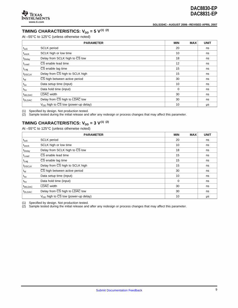
TIMING CHARACTERISTICS: VDD = 5 V (1) (2)
TIMING CHARACTERISTICS: VDD = 3 V (1) (2)
DAC8830-EPDAC8831-EP
SGLS334C–AUGUST 2006–REVISED APRIL 2007
At –55°C to 125°C (unless otherwise noted)
PARAMETER MIN MAX UNIT
tsck SCLK period 20 ns
twsck SCLK high or low time 10 ns
tDelay Delay from SCLK high to CS low 18 ns
tLead CS enable lead time 12 ns
tLag CS enable lag time 15 ns
tDSCLK Delay from CS high to SCLK high 15 ns
ttd CS high between active period 30 ns
tsu Data setup time (input) 10 ns
tho Data hold time (input) 0 ns
tWLDAC LDAC width 30 ns
tDLDAC Delay from CS high to LDAC low 30 ns
VDD high to CS low (power-up delay) 10 μs
(1) Specified by design. Not production tested.(2) Sample tested during the initial release and after any redesign or process changes that may affect this parameter.
At –55°C to 125°C (unless otherwise noted)
PARAMETER MIN MAX UNIT
tsck SCLK period 20 ns
twsck SCLK high or low time 10 ns
tDelay Delay from SCLK high to CS low 18 ns
tLead CS enable lead time 15 ns
tLag CS enable lag time 15 ns
tDSCLK Delay from CS high to SCLK high 15 ns
ttd CS high between active period 30 ns
tsu Data setup time (input) 10 ns
tho Data hold time (input) 0 ns
tWLDAC LDAC width 30 ns
tDLDAC Delay from CS high to LDAC low 30 ns
VDD high to CS low (power-up delay) 10 μs
(1) Specified by design. Not production tested.(2) Sample tested during the initial release and after any redesign or process changes that may affect this parameter.
9Submit Documentation Feedback

www.ti.com
TYPICAL CHARACTERISTICS: VDD = 5 V
81920 65536573444915240960327682457616384Digital Input Code
TA = +25CVREF = 2.5 V
1.00
0.75
0.50
0.25
0
−0.25
−0.50
−0.75
−1.00
INL
(LS
B)
81920 65536573444915240960327682457616384Digital Input Code
TA = +25CVREF = 2.5 V
1.00
0.75
0.50
0.25
0
−0.25
−0.50
−0.75
−1.00
DN
L(L
SB
)
81920
1.00
0.75
0.50
0.25
0
−0.25
−0.50
−0.75
−1.0065536573444915240960327682457616384
Digital Input Code
INL
(LS
B)
TA = −40CVREF = 2.5 V
81920 65536573444915240960327682457616384Digital Input Code
TA = −40CVREF = 2.5 V
1.00
0.75
0.50
0.25
0
−0.25
−0.50
−0.75
−1.00
DN
L(L
SB
)
81920 65536573444915240960327682457616384Digital Input Code
TA = +85CVREF = 2.5 V
1.00
0.75
0.50
0.25
0
−0.25
−0.50
−0.75
−1.00
INL
(LS
B)
81920 65536573444915240960327682457616384Digital Input Code
TA = +85CVREF = 2.5 V
1.00
0.75
0.50
0.25
0
−0.25
−0.50
−0.75
−1.00
DN
L(L
SB
)
DAC8830-EPDAC8831-EP
SGLS334C–AUGUST 2006–REVISED APRIL 2007
At TA = 25°C, VREF = 2.5 V (unless otherwise noted)
LINEARITY ERROR DIFFERENTIAL LINEARITY ERRORvs DIGITAL INPUT CODE vs DIGITAL INPUT CODE
Figure 4. Figure 5.
LINEARITY ERROR DIFFERENTIAL LINEARITY ERRORvs DIGITAL INPUT CODE vs DIGITAL INPUT CODE
Figure 6. Figure 7.
LINEARITY ERROR DIFFERENTIAL LINEARITY ERRORvs DIGITAL INPUT CODE vs DIGITAL INPUT CODE
Figure 8. Figure 9.
10 Submit Documentation Feedback

www.ti.com
81920 65536573444915240960327682457616384Digital Input Code
TA = +25CVREF = 5 V
1.00
0.75
0.50
0.25
0
−0.25
−0.50
−0.75
−1.00
INL
(LS
B)
81920 65536573444915240960327682457616384Digital Input Code
TA = +25CVREF = 5 V
1.00
0.75
0.50
0.25
0
−0.25
−0.50
−0.75
−1.00
DN
L(L
SB
)
0.75
0.50
0.25
0
−0.25
−0.50
Lin
eari
tyE
rror
(LS
B)
Reference Voltage (V)
0 2 4 6531
INL
DNL
0.75
0.50
0.25
0
−0.25
−0.50
Lin
eari
tyE
rror
(LS
B)
Supply Voltage (V)
2.5 3.0 3.5 4.0 4.5 5.0 5.5 6.0
VREF = 2.5 V
DNL
INL
−60 −40 −20 0 20 40 60 80 140120100Temperature (C)
VREF = 2.5 V
Bipolar Mode
Unipolar Mode
1.25
1.00
0.75
0.50
0.25
0
−0.25
−0.50
−0.75
Ga
inE
rror
(LS
B)
−60 −40 −20 0 20 40 60 80 140120100Temperature (C)
VREF = 2.5 V
Bipolar Mode
Unipolar Mode
0.50
0.25
0
−0.25
−0.50
Ze
ro−
Cod
eE
rro
r(L
SB
)
DAC8830-EPDAC8831-EP
SGLS334C–AUGUST 2006–REVISED APRIL 2007
TYPICAL CHARACTERISTICS: VDD = 5 V (continued)At TA = 25°C, VREF = 2.5 V (unless otherwise noted)
LINEARITY ERROR DIFFERENTIAL LINEARITY ERRORvs DIGITAL INPUT CODE vs DIGITAL INPUT CODE
Figure 10. Figure 11.
LINEARITY ERROR LINEARITY ERRORvs REFERENCE VOLTAGE vs SUPPLY VOLTAGE
Figure 12. Figure 13.
GAIN ERROR ZERO-CODE ERRORvs TEMPERATURE vs TEMPERATURE
Figure 14. Figure 15.
11Submit Documentation Feedback

www.ti.com
81920
300
250
200
150
100
50
065536573444915240960327682457616384
Digital Input Code
Ref
ere
nce
Cur
rent
(µA
)
VREF = 2.5 V
81920
300
250
200
150
100
50
065536573444915240960327682457616384
Digital Input Code
Ref
eren
ceC
urre
nt(
µ A)
VREF = 2.5 V
0 1 2 3 4 5Digital Input Voltage (V)
VDD = 5 V
VDD = 3 V
800
700
600
500
400
300
200
100
0
Sup
ply
Cu
rren
t(µ
A)
−60 −40 −20 0 20 40 60 80 140120100Temperature (C)
VDD = 5 VVLOGIC = 5 V
VDD = 3 VVLOGIC = 3 V
VREF = 2.5 V
5
4
3
2
1
0
Sup
ply
Cur
ren
t(µ A
)
2.7 3.0 3.3 3.6 3.9 4.2 4.5 4.8 5.1 5.4 5.7 6.0Supply Voltage (V)
VREF = 2.5 V5.0
4.5
4.0
3.5
3.0
2.5
2.0
1.5
1.0
0.5
0
Sup
ply
Cur
rent
(µA
)
0 0.5 1.0 1.5 2.0 2.5 3.0 3.5 4.54.0 5.0Reference Voltage (V)
VDD = 5 V
VDD = 3 V
5.0
4.5
4.0
3.5
3.0
2.5
2.0
1.5
1.0
0.5
0
Sup
ply
Cur
rent
(µA
)
DAC8830-EPDAC8831-EP
SGLS334C–AUGUST 2006–REVISED APRIL 2007
TYPICAL CHARACTERISTICS: VDD = 5 V (continued)At TA = 25°C, VREF = 2.5 V (unless otherwise noted)
REFERENCE CURRENT REFERENCE CURRENTvs CODE (UNIPOLAR MODE) vs CODE (BIPOLAR MODE)
Figure 16. Figure 17.
SUPPLY CURRENT SUPPLY CURRENTvs DIGITAL INPUT VOLTAGE vs TEMPERATURE
Figure 18. Figure 19.
SUPPLY CURRENT SUPPLY CURRENTvs SUPPLY VOLTAGE vs REFERENCE VOLTAGE
Figure 20. Figure 21.
12 Submit Documentation Feedback

www.ti.com
5V/div
0.1V/div
Time (0.5µs/div)
LDAC
VOUT
VREF = 2.5 V
Time (0.5µs/div)
VREF = 2.5 V
LDAC
VOUT
5V/div
0.1V/div
Time (0.2µs/div)
VREF = 2.5 V
LDAC
VOUT
5V/div
1V/div
Time (0.2µs/div)
VREF = 2.5 V
LDAC
VOUT
5V/div
1V/div
Time (50ns/div)
VREF = 2.5 V
SDI
VOUT
5V/div
20mV/div
DAC8830-EPDAC8831-EP
SGLS334C–AUGUST 2006–REVISED APRIL 2007
TYPICAL CHARACTERISTICS: VDD = 5 V (continued)At TA = 25°C, VREF = 2.5 V (unless otherwise noted)
MAJOR-CARRY GLITCH MAJOR-CARRY GLITCH(FALLING) (RISING)
Figure 22. Figure 23.
DAC SETTLING TIME DAC SETTLING TIME(FALLING) (RISING)
Figure 24. Figure 25.
DIGITALFEEDTHROUGH
Figure 26.
13Submit Documentation Feedback

www.ti.com
TYPICAL CHARACTERISTICS: VDD = 3 V
81920 65536573444915240960327682457616384Digital Input Code
TA = +25CVREF = 1.5 V
1.00
0.75
0.50
0.25
0
−0.25
−0.50
−0.75
−1.00
INL
(LS
B)
81920 65536573444915240960327682457616384Digital Input Code
TA = +25CVREF = 1.5 V
1.00
0.75
0.50
0.25
0
−0.25
−0.50
−0.75
−1.00
DN
L(L
SB
)
81920 65536573444915240960327682457616384Digital Input Code
TA = −40CVREF = 1.5 V
1.00
0.75
0.50
0.25
0
−0.25
−0.50
−0.75
−1.00
INL
(LS
B)
81920 65536573444915240960327682457616384Digital Input Code
TA = −40CVREF = 1.5 V
1.00
0.75
0.50
0.25
0
−0.25
−0.50
−0.75
−1.00
DN
L(L
SB
)
81920 65536573444915240960327682457616384Digital Input Code
TA = +85CVREF = 1.5 V
1.00
0.75
0.50
0.25
0
−0.25
−0.50
−0.75
−1.00
INL
(LS
B)
81920 65536573444915240960327682457616384Digital Input Code
TA = +85CVREF = 1.5 V
1.00
0.75
0.50
0.25
0
−0.25
−0.50
−0.75
−1.00
DN
L(L
SB
)
DAC8830-EPDAC8831-EP
SGLS334C–AUGUST 2006–REVISED APRIL 2007
At TA = 25°C, VREF = 2.5 V (unless otherwise noted)
LINEARITY ERROR DIFFERENTIAL LINEARITY ERRORvs DIGITAL INPUT CODE vs DIGITAL INPUT CODE
Figure 27. Figure 28.
LINEARITY ERROR DIFFERENTIAL LINEARITY ERRORvs DIGITAL INPUT CODE vs DIGITAL INPUT CODE
Figure 29. Figure 30.
LINEARITY ERROR DIFFERENTIAL LINEARITY ERRORvs DIGITAL INPUT CODE vs DIGITAL INPUT CODE
Figure 31. Figure 32.
14 Submit Documentation Feedback

www.ti.com
81920 65536573444915240960327682457616384Digital Input Code
TA = +25CVREF = 3 V
1.00
0.75
0.50
0.25
0
−0.25
−0.50
−0.75
−1.00
INL
(LS
B)
81920 65536573444915240960327682457616384Digital Input Code
TA = +25CVREF = 3 V
1.00
0.75
0.50
0.25
0
−0.25
−0.50
−0.75
−1.00
DN
L(L
SB
)
−60 −40 −20 0 20 40 60 80 140120100Temperature (C)
VDD = 3 VVREF = 2.5 V
Bipolar Mode
Unipolar Mode
1.00
0.75
0.50
0.25
0
−0.25
−0.50
−0.75
−1.00
Ga
inE
rror
(LS
B)
0.75
0.50
0.25
0
−0.25
−0.50
Lin
eari
tyE
rror
(LS
B)
Reference Voltage (V)
0.5 1.5 2.5 3.53.02.01.0
DNL
INL
−60 −40 −20 0 20 40 60 80 140120100Temperature (C)
VDD = 3 VVREF = 2.5 V
Bipolar Mode
Unipolar Mode
0.50
0.25
0
−0.25
−0.50
−0.75
Ze
ro−
Cod
eE
rro
r(L
SB
)
81920
300
250
200
150
100
50
065536573444915240960327682457616384
Digital Input Code
Ref
ere
nce
Cu
rre
nt(µ
A)
VREF = 1.5 V
DAC8830-EPDAC8831-EP
SGLS334C–AUGUST 2006–REVISED APRIL 2007
TYPICAL CHARACTERISTICS: VDD = 3 V (continued)At TA = 25°C, VREF = 2.5 V (unless otherwise noted)
LINEARITY ERROR DIFFERENTIAL LINEARITY ERRORvs DIGITAL INPUT CODE vs DIGITAL INPUT CODE
Figure 33. Figure 34.
LINEARITY ERROR GAIN ERRORvs REFERENCE VOLTAGE vs TEMPERATURE
Figure 35. Figure 36.
ZERO-CODE ERROR REFERENCE CURRENTvs TEMPERATURE vs CODE (UNIPOLAR MODE)
Figure 37. Figure 38.
15Submit Documentation Feedback

www.ti.com
Time (50ns/div)
VREF = 2.5 V
SDI
VOUT
5V/div
20mV/div
81920
300
250
200
150
100
50
065536573444915240960327682457616384
Digital Input Code
Ref
ere
nce
Cu
rre
nt(µ
A)
VREF = 1.5 V
Time (0.5µs/div)
LDAC
VOUT
VREF = 2.5 V
5V/div
0.1V/div
Time (0.5µs/div)
VREF = 2.5 V
LDAC
VOUT
5V/div
0.1V/div
Time (0.2µs/div)
VREF = 2.5 V
LDAC
VOUT
5V/div
1V/div
Time (0.2µs/div)
VREF = 2.5 V
LDAC
VOUT
5V/div
1V/div
DAC8830-EPDAC8831-EP
SGLS334C–AUGUST 2006–REVISED APRIL 2007
TYPICAL CHARACTERISTICS: VDD = 3 V (continued)At TA = 25°C, VREF = 2.5 V (unless otherwise noted)
REFERENCE CURRENT DIGITALvs CODE (BIPOLAR MODE) FEEDTHROUGH
Figure 39. Figure 40.
MAJOR-CARRY GLITCH MAJOR-CARRY GLITCH(FALLING) (RISING)
Figure 41. Figure 42.
DAC SETTLING TIME DAC SETTLING TIME(FALLING) (RISING)
Figure 43. Figure 44.
16 Submit Documentation Feedback

www.ti.com
THEORY OF OPERATION
General Description
Digital-to-Analog Sections
R R
12−Bit R−2R Ladder Four MSBs Decoded into15 Equal Segments
2R2R 2R 2R
S0 S1 S11
2R
VOUT
E15
2R
E2
2R
E1
VREF
Output Range
DAC8830-EPDAC8831-EP
SGLS334C–AUGUST 2006–REVISED APRIL 2007
The DAC8830 and DAC8831 are single, 16-bit, serial-input, voltage-output DACs. They operate from a singlesupply ranging from 2.7 V to 5 V, and typically consume 5 μA. Data is written to these devices in a 16-bit wordformat, via an SPI serial interface. To ensure a known power-up state, these parts were designed with apower-on reset function. The DAC8830 and DAC8831 are reset to zero code. In unipolar mode, the DAC8830and DAC8831 are reset to 0V, and in bipolar mode, the DAC8831 is reset to –VREF. Kelvin sense connectionsfor the reference and analog ground are included on the DAC8831.
The DAC architecture for both devices consists of two matched DAC sections and is segmented. A simplifiedcircuit diagram is shown in Figure 45. The four MSBs of the 16-bit data word are decoded to drive 15 switches,E1 to E15. Each of these switches connects one of 15 matched resistors to either AGND or VREF. The remaining12 bits of the data word drive switches S0 to S11 of a 12-bit voltage mode R-2R ladder network.
Figure 45. DAC Architecture
The output of the DAC isVOUT = (VREF × Code/65536)
Where:
Code = Decimal data word loaded to the DAC latch
17Submit Documentation Feedback
www.ti.com
Power-on Reset
Serial Interface
DAC8830-EPDAC8831-EP
SGLS334C–AUGUST 2006–REVISED APRIL 2007
THEORY OF OPERATION (continued)
Both devices have a power-on reset function to ensure the output is at a known state upon power up. In theDAC8830 and DAC8831, on power up, the DAC latch and input registers contain all 0s until new data is loadedfrom the input serial shift register. Therefore, after power up, the output from pin VOUT of the DAC8830 is 0 V.The output from pin VOUT of the DAC8831 is 0 V in unipolar mode and –VREF in bipolar mode.
However, the serial register of the DAC8830 and DAC8831 is not cleared on power up, so its contents areundefined. When loading data initially to the device, 16 bits or more should be loaded to prevent erroneous dataappearing on the output. If more than 16 bits are loaded, the last 16 are kept; if less than 16 are loaded, bits willremain from the previous word. If the device must be interfaced with data shorter than 16 bits, the data shouldbe padded with 0s at the LSBs.
The digital interface is standard 3-wire connection compatible with SPI, QSPI, Microwire, and Texas InstrumentsDSP interfaces, which can operate at speeds up to 50 Mbps. The data transfer is framed by CS, the chip selectsignal. The DAC works as a bus slave. The bus master generates the synchronize clock, SCLK, and initiates thetransmission. When CS is high, the DAC is not accessed, and the clock SCLK and serial input data SDI areignored. The bus master accesses the DAC by driving pin CS low. Immediately following the high-to-lowtransition of CS, the serial input data on pin SDI is shifted out from the bus master synchronously on the fallingedge of SCLK, and latched on the rising edge of SCLK into the input shift register, MSB first. The low-to-hightransition of CS transfers the contents of the input shift register to the input register. All data registers are 16 bit.It takes 16 clocks of SCLK to transfer one data word to the parts. To complete a whole data word, CS must gohigh immediately after 16 SCLKs are clocked in. If more than 16 SCLKs are applied during the low state of CS,the last 16 bits are transferred to the input register on the rising edge of CS. However, if CS is not kept lowduring the entire 16 SCLK cycles, data is corrupted. In this case, reload the DAC latch with a new 16-bit word.
In the DAC8830, the contents of the input register are transferred into the DAC latch immediately when the inputregister is loaded, and the DAC output is updated at the same time.
The DAC8831 has an LDAC pin allowing the DAC latch to be updated asynchronously by bringing LDAC lowafter CS goes high. In this case, LDAC must be maintained high while CS is low. If LDAC is tied permanentlylow, the DAC latch is updated immediately after the input register is loaded (caused by the low-to-high transitionof CS).
18 Submit Documentation Feedback

www.ti.com
APPLICATION INFORMATION
Unipolar Output Operation
DAC
DAC8830
SDI
SCLK
CS
DGND
VOUT
0.1 µF
VO = 0 to +VREF
AGND
Ser
ial
Inte
rfac
e
InputRegister DAC Latch
VDD VREF
+5 V +2.5 V
OPA277OPA704OPA727
+0.1 µF 10 µF
DAC8830-EPDAC8831-EP
SGLS334C–AUGUST 2006–REVISED APRIL 2007
These DACs are capable of driving unbuffered loads of 60 kΩ. Unbuffered operation results in low supplycurrent (typically 5 μA) and a low offset error. The DAC8830 provides a unipolar output swing ranging from 0 Vto VREF. The DAC8831 can be configured to output both unipolar and bipolar voltages. Figure 46 and Figure 47show a typical unipolar output voltage circuit for each device, respectively. The code table for this mode ofoperation is shown in Table 1.
Table 1. Unipolar Code
DAC Latch ContentsAnalog Output
MSB LSB
1111 1111 1111 1111 VREF × (65,535/65,536)
1000 0000 0000 0000 VREF × (32,768/65,536) = VREF
0000 0000 0000 0001 VREF × (1/65,536)
0000 0000 0000 0000 0 V
Figure 46. Unipolar Output Mode of DAC8830
19Submit Documentation Feedback

www.ti.com
0.1 µF
VDD
+5 V
RFB
INV
AGNDF
AGNDS
DAC
DAC LatchInput
Register
DAC8831
+V
−V
SDI
SCLK
LDAC
VOUT
RFBRINV
VREF−S VREF−F
Ser
ialI
nter
face
and
Con
trol
Logi
c
CS
+2.5 V
+0.1 µF 10 µF
DGND
VO = 0 to +VREF
OPA277OPA704OPA727
VOUT_UNI D
216 VREF VGE
VZSE INL
DAC8830-EPDAC8831-EP
SGLS334C–AUGUST 2006–REVISED APRIL 2007
Figure 47. Unipolar Output Mode of DAC8831
Assuming a perfect reference, the worst-case output voltage may be calculated from the following equation:
Unipolar Mode Worst-Case Output
Where:VOUT_UNI = Unipolar mode worst-case outputD = Code loaded to DACVREF = Reference voltage applied to partVGE = Gain error in voltsVZSE = Zero scale error in voltsINL = Integral nonlinearity in volts
20 Submit Documentation Feedback
www.ti.com
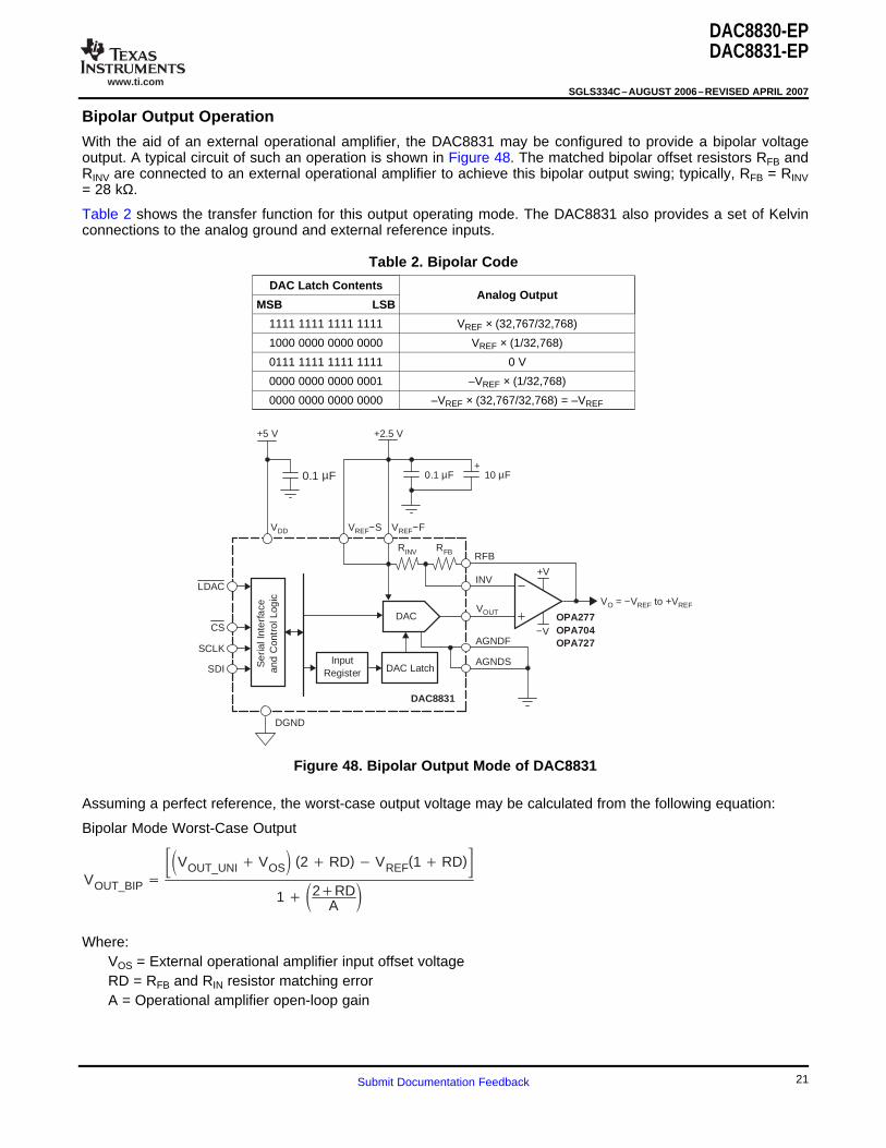
Bipolar Output Operation
0.1 µF
VDD
+5 V
RFB
INV
AGNDF
AGNDS
DAC
DAC LatchInput
Register
DAC8831
+V
−V
SDI
SCLK
LDAC
VOUT
RFBRINV
VREF−S VREF−F
Se
rialI
nte
rfa
cean
dC
ontr
olLo
gic
CS
+2.5 V
+0.1 µF 10 µF
DGND
VO = −VREF to +VREF
OPA277OPA704OPA727
VOUT_BIP VOUT_UNI VOS
(2 RD) VREF(1 RD)1 2RD
A
DAC8830-EPDAC8831-EP
SGLS334C–AUGUST 2006–REVISED APRIL 2007
With the aid of an external operational amplifier, the DAC8831 may be configured to provide a bipolar voltageoutput. A typical circuit of such an operation is shown in Figure 48. The matched bipolar offset resistors RFB andRINV are connected to an external operational amplifier to achieve this bipolar output swing; typically, RFB = RINV= 28 kΩ.
Table 2 shows the transfer function for this output operating mode. The DAC8831 also provides a set of Kelvinconnections to the analog ground and external reference inputs.
Table 2. Bipolar Code
DAC Latch ContentsAnalog Output
MSB LSB
1111 1111 1111 1111 VREF × (32,767/32,768)
1000 0000 0000 0000 VREF × (1/32,768)
0111 1111 1111 1111 0 V
0000 0000 0000 0001 –VREF × (1/32,768)
0000 0000 0000 0000 –VREF × (32,767/32,768) = –VREF
Figure 48. Bipolar Output Mode of DAC8831
Assuming a perfect reference, the worst-case output voltage may be calculated from the following equation:
Bipolar Mode Worst-Case Output
Where:VOS = External operational amplifier input offset voltageRD = RFB and RIN resistor matching errorA = Operational amplifier open-loop gain
21Submit Documentation Feedback
www.ti.com
Output Amplifier Selection
Reference and Ground
Power Supply and Reference Bypassing
DAC8830-EPDAC8831-EP
SGLS334C–AUGUST 2006–REVISED APRIL 2007
For bipolar mode, a precision amplifier should be used, supplied from a dual power supply. This provides the±VREF output.
In a single-supply application, selection of a suitable operational amplifier may be more difficult because theoutput swing of the amplifier does not usually include the negative rail; in this case, AGND. This output swingcan result in some degradation of the specified performance unless the application does not use codes near 0.
The selected operational amplifier needs to have low-offset voltage (the DAC LSB is 38 μV with a 2.5-Vreference), eliminating the need for output offset trims. Input bias current should also be low because the biascurrent multiplied by the DAC output impedance (approximately 6.25 kΩ) adds to the zero-code error.
Rail-to-rail input and output performance is required. For fast settling, the slew rate of the operational amplifiershould not impede the settling time of the DAC. Output impedance of the DAC is constant andcode-independent, but in order to minimize gain errors the input impedance of the output amplifier should be ashigh as possible. The amplifier should also have a 3 dB bandwidth of 1 MHz or greater. The amplifier addsanother time constant to the system, thus increasing the settling time of the output. A higher 3-dB amplifierbandwidth results in a shorter effective settling time of the combined DAC and amplifier.
Since the input impedance is code-dependent, the reference pin should be driven from a low impedance source.The DAC8830 and DAC8831 operate with a voltage reference ranging from 1.25 V to VDD. References below1.25 V result in reduced accuracy.
The DAC full-scale output voltage is determined by the reference. Table 1 and Table 2 outline the analog outputvoltage for particular digital codes.
For optimum performance, Kelvin sense connections are provided on the DAC8831. If the application does notrequire separate force and sense lines, they should be tied together close to the package to minimize voltagedrops between the package leads and the internal die.
For accurate high-resolution performance, it is recommended that the reference and supply pins be bypassedwith a 10 μF tantalum capacitor in parallel with a 0.1 μF ceramic capacitor.
22 Submit Documentation Feedback

www.ti.com
CROSS REFERENCE
DAC8830-EPDAC8831-EP
SGLS334C–AUGUST 2006–REVISED APRIL 2007
The DAC8830 and DAC8831 have an industry-standard pinout configuration (see Table 3).
Table 3. Cross ReferenceINL DNL POWER-ON TEMPERATURE PACKAGE PACKAGE CROSSMODEL (LSB) (LSB) RESET TO RANGE DESCRIPTION OPTION REFERENCE
AD5541CR,DAC8830ICD ±1 ±1 Zero-Code –40°C to 85°C 8-Lead Small Outline IC SO-8 MAX541AESA
AD5541BR,DAC8830IBD ±2 ±1 Zero-Code –40°C to 85°C 8-Lead Small Outline IC SO-8 MAX541BESA
AD5541AR,DAC8830ID ±4 ±1 Zero-Code –40°C to 85°C 8-Lead Small Outline IC SO-8 MAX541CESA
DAC8830MCD ±1 ±1 Zero-Code –55°C to 125°C 8-Lead Small Outline IC SO-8 N/A
N/A ±1 ±1 Zero-Code –40°C to 85°C 8-Lead Plastic DIP PDIP-8 MAX541AEPA
N/A ±2 ±1 Zero-Code –40°C to 85°C 8-Lead Plastic DIP PDIP-8 MAX541BEPA
N/A ±4 ±1 Zero-Code –40°C to 85°C 8-Lead Plastic DIP PDIP-8 MAX541CEPA
N/A ±1 ±1 Zero-Code 0°C to 70°C 8-Lead Small Outline IC SO-8 AD5541LR
N/A ±2 ±1.5 Zero-Code 0°C to 70°C 8-Lead Small Outline IC SO-8 AD5541JR
N/A ±1 ±1 Zero-Code 0°C to 70°C 8-Lead Plastic DIP PDIP-8 MAX541AEPA
N/A ±2 ±1 Zero-Code 0°C to 70°C 8-Lead Plastic DIP PDIP-8 MAX541BEPA
N/A ±4 ±1 Zero-Code 0°C to 70°C 8-Lead Plastic DIP PDIP-8 MAX541CEPA
AD5542CR,DAC8831ICD ±1 ±1 Zero-Code –40°C to 85°C 14-Lead Small Outline IC SO-14 MAX542AESD
AD5542BR,DAC8831IBD ±2 ±1 Zero-Code –40°C to 85°C 14-Lead Small Outline IC SO-14 MAX542BESD
AD5542AR,DAC8831ID ±4 ±1 Zero-Code –40°C to 85°C 14-Lead Small Outline IC SO-14 MAX542CESD
DAC8831MCD ±1 ±1 Zero-Code –55°C to 125°C 14-Lead Small Outline IC SO-14 N/A
N/A ±1 ±1 Zero-Code –40°C to 85°C 14-Lead Plastic DIP PDIP-14 MAX542ACPD
N/A ±2 ±1 Zero-Code –40°C to 85°C 14-Lead Plastic DIP PDIP-14 MAX542BCPD
N/A ±4 ±1 Zero-Code –40°C to 85°C 14-Lead Plastic DIP PDIP-14 MAX542CCPD
N/A ±4 ±1 Zero-Code –55°C to 125°C 14-Lead Ceramic SB SB-14 MAX542CMJD
N/A ±1 ±1 Zero-Code 0°C to 70°C 14-Lead Small Outline IC SO-14 AD5542LR
N/A ±2 ±1.5 Zero-Code 0°C to 70°C 14-Lead Small Outline IC SO-14 AD5542JR
N/A ±1 ±1 Zero-Code 0°C to 70°C 14-Lead Small Outline IC SO-14 MAX542AEPD
N/A ±2 ±1 Zero-Code 0°C to 70°C 14-Lead Small Outline IC SO-14 MAX542BEPD
N/A ±4 ±1 Zero-Code 0°C to 70°C 14-Lead Small Outline IC SO-14 MAX542CEPD
23Submit Documentation Feedback

PACKAGE OPTION ADDENDUM
www.ti.com 31-May-2014
Addendum-Page 1
PACKAGING INFORMATION
Orderable Device Status(1)
Package Type PackageDrawing
Pins PackageQty
Eco Plan(2)
Lead/Ball Finish(6)
MSL Peak Temp(3)
Op Temp (°C) Device Marking(4/5)
Samples
DAC8830MCDEP ACTIVE SOIC D 8 75 Green (RoHS& no Sb/Br)
CU NIPDAU Level-3-260C-168 HR -55 to 125 8830EP
DAC8830MCDREP ACTIVE SOIC D 8 2500 Green (RoHS& no Sb/Br)
CU NIPDAU Level-3-260C-168 HR -55 to 125 8830EP
DAC8831MCDEP ACTIVE SOIC D 14 50 Green (RoHS& no Sb/Br)
CU NIPDAU Level-3-260C-168 HR -55 to 125 8831EP
DAC8831MCDREP ACTIVE SOIC D 14 2500 Green (RoHS& no Sb/Br)
CU NIPDAU Level-3-260C-168 HR -55 to 125 8831EP
V62/06671-01XE ACTIVE SOIC D 8 2500 Green (RoHS& no Sb/Br)
CU NIPDAU Level-3-260C-168 HR -55 to 125 8830EP
V62/06671-02XE ACTIVE SOIC D 8 75 Green (RoHS& no Sb/Br)
CU NIPDAU Level-3-260C-168 HR -55 to 125 8830EP
V62/06671-03YE ACTIVE SOIC D 14 2500 Green (RoHS& no Sb/Br)
CU NIPDAU Level-3-260C-168 HR -55 to 125 8831EP
V62/06671-04YE ACTIVE SOIC D 14 50 Green (RoHS& no Sb/Br)
CU NIPDAU Level-3-260C-168 HR -55 to 125 8831EP
(1) The marketing status values are defined as follows:ACTIVE: Product device recommended for new designs.LIFEBUY: TI has announced that the device will be discontinued, and a lifetime-buy period is in effect.NRND: Not recommended for new designs. Device is in production to support existing customers, but TI does not recommend using this part in a new design.PREVIEW: Device has been announced but is not in production. Samples may or may not be available.OBSOLETE: TI has discontinued the production of the device.
(2) Eco Plan - The planned eco-friendly classification: Pb-Free (RoHS), Pb-Free (RoHS Exempt), or Green (RoHS & no Sb/Br) - please check http://www.ti.com/productcontent for the latest availabilityinformation and additional product content details.TBD: The Pb-Free/Green conversion plan has not been defined.Pb-Free (RoHS): TI's terms "Lead-Free" or "Pb-Free" mean semiconductor products that are compatible with the current RoHS requirements for all 6 substances, including the requirement thatlead not exceed 0.1% by weight in homogeneous materials. Where designed to be soldered at high temperatures, TI Pb-Free products are suitable for use in specified lead-free processes.Pb-Free (RoHS Exempt): This component has a RoHS exemption for either 1) lead-based flip-chip solder bumps used between the die and package, or 2) lead-based die adhesive used betweenthe die and leadframe. The component is otherwise considered Pb-Free (RoHS compatible) as defined above.Green (RoHS & no Sb/Br): TI defines "Green" to mean Pb-Free (RoHS compatible), and free of Bromine (Br) and Antimony (Sb) based flame retardants (Br or Sb do not exceed 0.1% by weightin homogeneous material)
(3) MSL, Peak Temp. - The Moisture Sensitivity Level rating according to the JEDEC industry standard classifications, and peak solder temperature.

PACKAGE OPTION ADDENDUM
www.ti.com 31-May-2014
Addendum-Page 2
(4) There may be additional marking, which relates to the logo, the lot trace code information, or the environmental category on the device.
(5) Multiple Device Markings will be inside parentheses. Only one Device Marking contained in parentheses and separated by a "~" will appear on a device. If a line is indented then it is a continuationof the previous line and the two combined represent the entire Device Marking for that device.
(6) Lead/Ball Finish - Orderable Devices may have multiple material finish options. Finish options are separated by a vertical ruled line. Lead/Ball Finish values may wrap to two lines if the finishvalue exceeds the maximum column width.
Important Information and Disclaimer:The information provided on this page represents TI's knowledge and belief as of the date that it is provided. TI bases its knowledge and belief on informationprovided by third parties, and makes no representation or warranty as to the accuracy of such information. Efforts are underway to better integrate information from third parties. TI has taken andcontinues to take reasonable steps to provide representative and accurate information but may not have conducted destructive testing or chemical analysis on incoming materials and chemicals.TI and TI suppliers consider certain information to be proprietary, and thus CAS numbers and other limited information may not be available for release.
In no event shall TI's liability arising out of such information exceed the total purchase price of the TI part(s) at issue in this document sold by TI to Customer on an annual basis.
OTHER QUALIFIED VERSIONS OF DAC8830-EP, DAC8831-EP :
• Catalog: DAC8830, DAC8831
NOTE: Qualified Version Definitions:
• Catalog - TI's standard catalog product

TAPE AND REEL INFORMATION
*All dimensions are nominal
Device PackageType
PackageDrawing
Pins SPQ ReelDiameter
(mm)
ReelWidth
W1 (mm)
A0(mm)
B0(mm)
K0(mm)
P1(mm)
W(mm)
Pin1Quadrant
DAC8830MCDREP SOIC D 8 2500 330.0 12.4 6.4 5.2 2.1 8.0 12.0 Q1
DAC8831MCDREP SOIC D 14 2500 330.0 16.4 6.5 9.0 2.1 8.0 16.0 Q1
PACKAGE MATERIALS INFORMATION
www.ti.com 17-Feb-2016
Pack Materials-Page 1

*All dimensions are nominal
Device Package Type Package Drawing Pins SPQ Length (mm) Width (mm) Height (mm)
DAC8830MCDREP SOIC D 8 2500 367.0 367.0 38.0
DAC8831MCDREP SOIC D 14 2500 367.0 367.0 38.0
PACKAGE MATERIALS INFORMATION
www.ti.com 17-Feb-2016
Pack Materials-Page 2


IMPORTANT NOTICE
Texas Instruments Incorporated and its subsidiaries (TI) reserve the right to make corrections, enhancements, improvements and otherchanges to its semiconductor products and services per JESD46, latest issue, and to discontinue any product or service per JESD48, latestissue. Buyers should obtain the latest relevant information before placing orders and should verify that such information is current andcomplete. All semiconductor products (also referred to herein as “components”) are sold subject to TI’s terms and conditions of salesupplied at the time of order acknowledgment.TI warrants performance of its components to the specifications applicable at the time of sale, in accordance with the warranty in TI’s termsand conditions of sale of semiconductor products. Testing and other quality control techniques are used to the extent TI deems necessaryto support this warranty. Except where mandated by applicable law, testing of all parameters of each component is not necessarilyperformed.TI assumes no liability for applications assistance or the design of Buyers’ products. Buyers are responsible for their products andapplications using TI components. To minimize the risks associated with Buyers’ products and applications, Buyers should provideadequate design and operating safeguards.TI does not warrant or represent that any license, either express or implied, is granted under any patent right, copyright, mask work right, orother intellectual property right relating to any combination, machine, or process in which TI components or services are used. Informationpublished by TI regarding third-party products or services does not constitute a license to use such products or services or a warranty orendorsement thereof. Use of such information may require a license from a third party under the patents or other intellectual property of thethird party, or a license from TI under the patents or other intellectual property of TI.Reproduction of significant portions of TI information in TI data books or data sheets is permissible only if reproduction is without alterationand is accompanied by all associated warranties, conditions, limitations, and notices. TI is not responsible or liable for such altereddocumentation. Information of third parties may be subject to additional restrictions.Resale of TI components or services with statements different from or beyond the parameters stated by TI for that component or servicevoids all express and any implied warranties for the associated TI component or service and is an unfair and deceptive business practice.TI is not responsible or liable for any such statements.Buyer acknowledges and agrees that it is solely responsible for compliance with all legal, regulatory and safety-related requirementsconcerning its products, and any use of TI components in its applications, notwithstanding any applications-related information or supportthat may be provided by TI. Buyer represents and agrees that it has all the necessary expertise to create and implement safeguards whichanticipate dangerous consequences of failures, monitor failures and their consequences, lessen the likelihood of failures that might causeharm and take appropriate remedial actions. Buyer will fully indemnify TI and its representatives against any damages arising out of the useof any TI components in safety-critical applications.In some cases, TI components may be promoted specifically to facilitate safety-related applications. With such components, TI’s goal is tohelp enable customers to design and create their own end-product solutions that meet applicable functional safety standards andrequirements. Nonetheless, such components are subject to these terms.No TI components are authorized for use in FDA Class III (or similar life-critical medical equipment) unless authorized officers of the partieshave executed a special agreement specifically governing such use.Only those TI components which TI has specifically designated as military grade or “enhanced plastic” are designed and intended for use inmilitary/aerospace applications or environments. Buyer acknowledges and agrees that any military or aerospace use of TI componentswhich have not been so designated is solely at the Buyer's risk, and that Buyer is solely responsible for compliance with all legal andregulatory requirements in connection with such use.TI has specifically designated certain components as meeting ISO/TS16949 requirements, mainly for automotive use. In any case of use ofnon-designated products, TI will not be responsible for any failure to meet ISO/TS16949.
Products ApplicationsAudio www.ti.com/audio Automotive and Transportation www.ti.com/automotiveAmplifiers amplifier.ti.com Communications and Telecom www.ti.com/communicationsData Converters dataconverter.ti.com Computers and Peripherals www.ti.com/computersDLP® Products www.dlp.com Consumer Electronics www.ti.com/consumer-appsDSP dsp.ti.com Energy and Lighting www.ti.com/energyClocks and Timers www.ti.com/clocks Industrial www.ti.com/industrialInterface interface.ti.com Medical www.ti.com/medicalLogic logic.ti.com Security www.ti.com/securityPower Mgmt power.ti.com Space, Avionics and Defense www.ti.com/space-avionics-defenseMicrocontrollers microcontroller.ti.com Video and Imaging www.ti.com/videoRFID www.ti-rfid.comOMAP Applications Processors www.ti.com/omap TI E2E Community e2e.ti.comWireless Connectivity www.ti.com/wirelessconnectivity
Mailing Address: Texas Instruments, Post Office Box 655303, Dallas, Texas 75265Copyright © 2016, Texas Instruments Incorporated