Embed Size (px)
Citation preview
For price, delivery and to place orders: Hittite Microwave Corporation, 2 Elizabeth Drive, Chelmsford, MA 01824Phone: 978-250-3343 Fax: 978-250-3373 Order On-line at www.hittite.com
Application Support: Phone: 978-250-3343 or [email protected]
lim
itin
g a
mp
lif
ier
s -
sm
t
1
HMC914LP4Ev03.1012
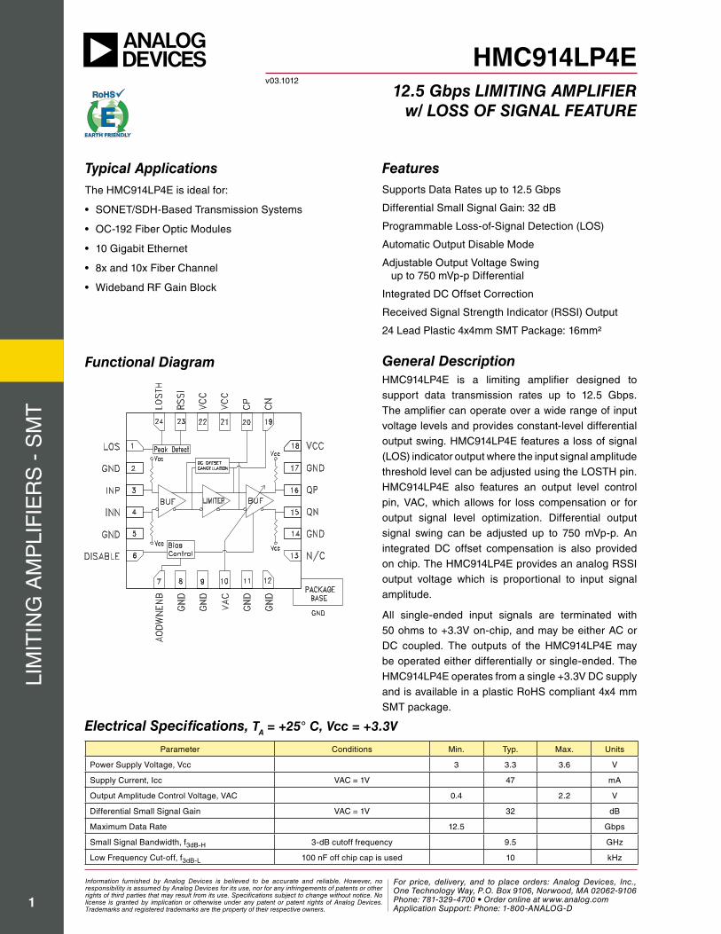
Functional Diagram
Electrical Specifications, TA = +25° C, Vcc = +3.3V
The HMC914LP4E is ideal for:
• SONET/SDH-Based Transmission Systems
• OC-192 Fiber Optic Modules
• 10 Gigabit Ethernet
• 8x and 10x Fiber Channel
• Wideband RF Gain Block
Supports Data Rates up to 12.5 Gbps
Differential Small Signal Gain: 32 dB
Programmable Loss-of-Signal Detection (LOS)
Automatic Output Disable Mode
Adjustable Output Voltage Swing up to 750 mVp-p Differential
Integrated DC Offset Correction
Received Signal Strength Indicator (RSSI) Output
24 Lead Plastic 4x4mm SMT Package: 16mm²
HMC914LP4E is a limiting amplifier designed to support data transmission rates up to 12.5 Gbps. The amplifier can operate over a wide range of input voltage levels and provides constant-level differential output swing. HMC914LP4E features a loss of signal (LOS) indicator output where the input signal amplitude threshold level can be adjusted using the LOSTH pin. HMC914LP4E also features an output level control pin, VAC, which allows for loss compensation or for output signal level optimization. Differential output signal swing can be adjusted up to 750 mVp-p. An integrated DC offset compensation is also provided on chip. The HMC914LP4E provides an analog RSSI output voltage which is proportional to input signal amplitude.
All single-ended input signals are terminated with 50 ohms to +3.3V on-chip, and may be either AC or DC coupled. The outputs of the HMC914LP4E may be operated either differentially or single-ended. The HMC914LP4E operates from a single +3.3V DC supply and is available in a plastic RoHS compliant 4x4 mm SMT package.
Parameter Conditions Min. Typ. Max. Units
Power Supply Voltage, Vcc 3 3.3 3.6 V
Supply Current, Icc VAC = 1V 47 mA
Output Amplitude Control Voltage, VAC 0.4 2.2 V
Differential Small Signal Gain VAC = 1V 32 dB
Maximum Data Rate 12.5 Gbps
Small Signal Bandwidth, f3dB-H 3-dB cutoff frequency 9.5 GHz
Low Frequency Cut-off, f3dB-L 100 nF off chip cap is used 10 kHz
Typical Applications Features
General Description
12.5 Gbps LIMITING AMPLIFIERw/ LOSS OF SIGNAL FEATURE
Information furnished by Analog Devices is believed to be accurate and reliable. However, no responsibility is assumed by Analog Devices for its use, nor for any infringements of patents or other rights of third parties that may result from its use. Specifications subject to change without notice. No license is granted by implication or otherwise under any patent or patent rights of Analog Devices. Trademarks and registered trademarks are the property of their respective owners.
For price, delivery, and to place orders: Analog Devices, Inc., One Technology Way, P.O. Box 9106, Norwood, MA 02062-9106 Phone: 781-329-4700 • Order online at www.analog.com Application Support: Phone: 1-800-ANALOG-D
For price, delivery and to place orders: Hittite Microwave Corporation, 2 Elizabeth Drive, Chelmsford, MA 01824Phone: 978-250-3343 Fax: 978-250-3373 Order On-line at www.hittite.com
Application Support: Phone: 978-250-3343 or [email protected]
lim
itin
g a
mp
lif
ier
s -
sm
t
2
HMC914LP4Ev03.1012
12.5 Gbps LIMITING AMPLIFIERw/ LOSS OF SIGNAL FEATURE
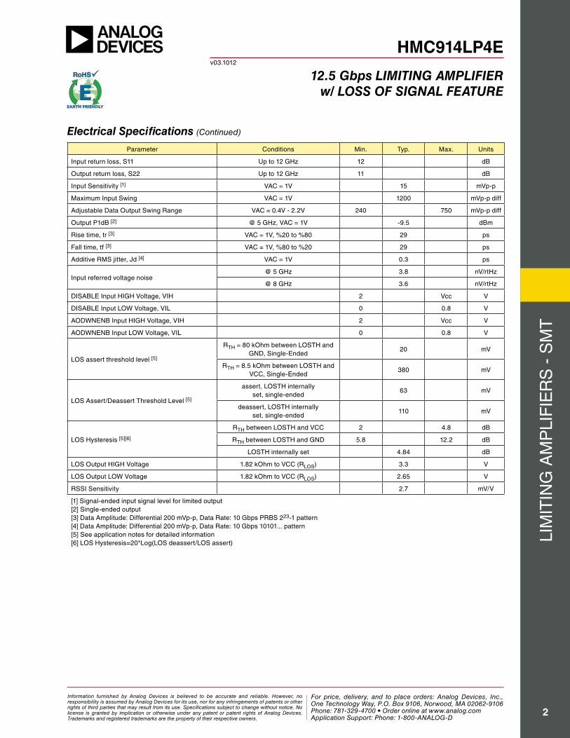
Parameter Conditions Min. Typ. Max. Units
Input return loss, S11 Up to 12 GHz 12 dB
Output return loss, S22 Up to 12 GHz 11 dB
Input Sensitivity [1] VAC = 1V 15 mVp-p
Maximum Input Swing VAC = 1V 1200 mVp-p diff
Adjustable Data Output Swing Range VAC = 0.4V - 2.2V 240 750 mVp-p diff
Output P1dB [2] @ 5 GHz, VAC = 1V -9.5 dBm
Rise time, tr [3] VAC = 1V, %20 to %80 29 ps
Fall time, tf [3] VAC = 1V, %80 to %20 29 ps
Additive RMS jitter, Jd [4] VAC = 1V 0.3 ps
Input referred voltage noise@ 5 GHz 3.8 nV/rtHz
@ 8 GHz 3.6 nV/rtHz
DISABLE Input HIGH Voltage, VIH 2 Vcc V
DISABLE Input LOW Voltage, VIL 0 0.8 V
AODWNENB Input HIGH Voltage, VIH 2 Vcc V
AODWNENB Input LOW Voltage, VIL 0 0.8 V
LOS assert threshold level [5]
RTH = 80 kOhm between LOSTH and GND, Single-Ended
20 mV
RTH = 8.5 kOhm between LOSTH and VCC, Single-Ended
380 mV
LOS Assert/Deassert Threshold Level [5]
assert, LOSTH internally set, single-ended
63 mV
deassert, LOSTH internallyset, single-ended
110 mV
LOS Hysteresis [5][6]
RTH between LOSTH and VCC 2 4.8 dB
RTH between LOSTH and GND 5.8 12.2 dB
LOSTH internally set 4.84 dB
LOS Output HIGH Voltage 1.82 kOhm to VCC (RLOS) 3.3 V
LOS Output LOW Voltage 1.82 kOhm to VCC (RLOS) 2.65 V
RSSI Sensitivity 2.7 mV/V
[1] Signal-ended input signal level for limited output[2] Single-ended output[3] Data Amplitude: Differential 200 mVp-p, Data Rate: 10 Gbps PRBS 223-1 pattern[4] Data Amplitude: Differential 200 mVp-p, Data Rate: 10 Gbps 10101... pattern[5] See application notes for detailed information[6] LOS Hysteresis=20*Log(LOS deassert/LOS assert)
Electrical Specifications (Continued)
Information furnished by Analog Devices is believed to be accurate and reliable. However, no responsibility is assumed by Analog Devices for its use, nor for any infringements of patents or other rights of third parties that may result from its use. Specifications subject to change without notice. No license is granted by implication or otherwise under any patent or patent rights of Analog Devices. Trademarks and registered trademarks are the property of their respective owners.
For price, delivery, and to place orders: Analog Devices, Inc., One Technology Way, P.O. Box 9106, Norwood, MA 02062-9106 Phone: 781-329-4700 • Order online at www.analog.com Application Support: Phone: 1-800-ANALOG-D
For price, delivery and to place orders: Hittite Microwave Corporation, 2 Elizabeth Drive, Chelmsford, MA 01824Phone: 978-250-3343 Fax: 978-250-3373 Order On-line at www.hittite.com
Application Support: Phone: 978-250-3343 or [email protected]
lim
itin
g a
mp
lif
ier
s -
sm
t
3
HMC914LP4Ev03.1012
12.5 Gbps LIMITING AMPLIFIERw/ LOSS OF SIGNAL FEATURE
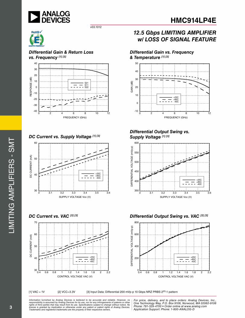
Differential Gain & Return Loss vs. Frequency [1] [2]
DC Current vs. Supply Voltage [1] [3]
DC Current vs. VAC [2] [3] Differential Output Swing vs. VAC [2] [3]
Differential Gain vs. Frequency & Temperature [1] [2]
Differential Output Swing vs. Supply Voltage [1] [3]
[1] VAC = 1V [2] VCC=3.3V [3] Input Data: Differential 200 mVp-p 10 Gbps NRZ PRBS 223-1 pattern
-40
-30
-20
-10
0
10
20
30
40
0 2 4 6 8 10 12
S21S11S22
FREQUENCY (GHz)
RE
SP
ON
SE
(dB
)
30
40
50
60
3 3.1 3.2 3.3 3.4 3.5 3.6
+25C+85C -40C
SUPPLY VOLTAGE Vcc (V)
DC
CU
RR
EN
T (
mA
)
30
40
50
60
70
0.4 0.6 0.8 1 1.2 1.4 1.6 1.8 2 2.2
+25C+85C-40C
CONTROL VOLTAGE VAC (V)
DC
CU
RR
EN
T (
mA
)
-10
0
10
20
30
40
50
0 2 4 6 8 10 12
+25C+85C -40C
FREQUENCY (GHz)
GA
IN (
dB)
350
400
450
500
550
600
3 3.1 3.2 3.3 3.4 3.5 3.6
+25C+85C -40C
SUPPLY VOLTAGE Vcc (V)
DIF
FE
RE
NT
IAL
VO
LTA
GE
(m
Vp-
p)
0
200
400
600
800
0.4 0.6 0.8 1 1.2 1.4 1.6 1.8 2 2.2
+25C+85C -40C
CONTROL VOLTAGE VAC (V)
DIF
FE
RE
NT
IAL
VO
LTA
GE
(m
Vp-
p)
Information furnished by Analog Devices is believed to be accurate and reliable. However, no responsibility is assumed by Analog Devices for its use, nor for any infringements of patents or other rights of third parties that may result from its use. Specifications subject to change without notice. No license is granted by implication or otherwise under any patent or patent rights of Analog Devices. Trademarks and registered trademarks are the property of their respective owners.
For price, delivery, and to place orders: Analog Devices, Inc., One Technology Way, P.O. Box 9106, Norwood, MA 02062-9106 Phone: 781-329-4700 • Order online at www.analog.com Application Support: Phone: 1-800-ANALOG-D
For price, delivery and to place orders: Hittite Microwave Corporation, 2 Elizabeth Drive, Chelmsford, MA 01824Phone: 978-250-3343 Fax: 978-250-3373 Order On-line at www.hittite.com
Application Support: Phone: 978-250-3343 or [email protected]
lim
itin
g a
mp
lif
ier
s -
sm
t
4
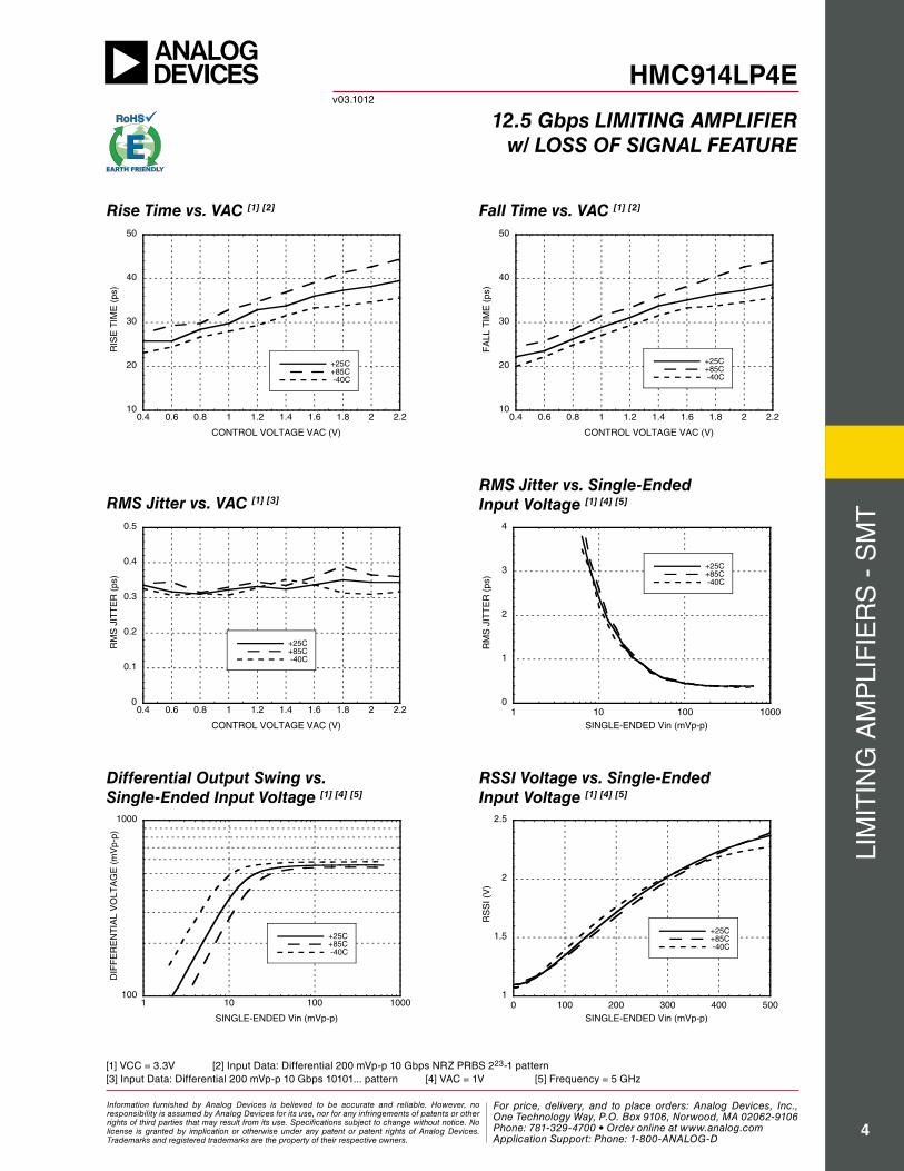
Rise Time vs. VAC [1] [2]
RMS Jitter vs. VAC [1] [3]
Fall Time vs. VAC [1] [2]
RMS Jitter vs. Single-Ended Input Voltage [1] [4] [5]
RSSI Voltage vs. Single-Ended Input Voltage [1] [4] [5]
Differential Output Swing vs. Single-Ended Input Voltage [1] [4] [5]
[1] VCC = 3.3V [2] Input Data: Differential 200 mVp-p 10 Gbps NRZ PRBS 223-1 pattern [3] Input Data: Differential 200 mVp-p 10 Gbps 10101... pattern [4] VAC = 1V [5] Frequency = 5 GHz
HMC914LP4Ev03.1012
12.5 Gbps LIMITING AMPLIFIERw/ LOSS OF SIGNAL FEATURE
10
20
30
40
50
0.4 0.6 0.8 1 1.2 1.4 1.6 1.8 2 2.2
+25C+85C -40C
CONTROL VOLTAGE VAC (V)
RIS
E T
IME
(ps
)
0
0.1
0.2
0.3
0.4
0.5
0.4 0.6 0.8 1 1.2 1.4 1.6 1.8 2 2.2
+25C+85C -40C
CONTROL VOLTAGE VAC (V)
RM
S J
ITT
ER
(ps
)
100
1000
1 10 100 1000
+25C+85C -40C
SINGLE-ENDED Vin (mVp-p)
DIF
FE
RE
NT
IAL
VO
LTA
GE
(m
Vp-
p)
10
20
30
40
50
0.4 0.6 0.8 1 1.2 1.4 1.6 1.8 2 2.2
+25C+85C -40C
CONTROL VOLTAGE VAC (V)
FA
LL T
IME
(ps
)
0
1
2
3
4
1 10 100 1000
+25C+85C -40C
SINGLE-ENDED Vin (mVp-p)
RM
S J
ITT
ER
(ps
)
1
1.5
2
2.5
0 100 200 300 400 500
+25C+85C -40C
SINGLE-ENDED Vin (mVp-p)
RS
SI (
V)
Information furnished by Analog Devices is believed to be accurate and reliable. However, no responsibility is assumed by Analog Devices for its use, nor for any infringements of patents or other rights of third parties that may result from its use. Specifications subject to change without notice. No license is granted by implication or otherwise under any patent or patent rights of Analog Devices. Trademarks and registered trademarks are the property of their respective owners.
For price, delivery, and to place orders: Analog Devices, Inc., One Technology Way, P.O. Box 9106, Norwood, MA 02062-9106 Phone: 781-329-4700 • Order online at www.analog.com Application Support: Phone: 1-800-ANALOG-D
For price, delivery and to place orders: Hittite Microwave Corporation, 2 Elizabeth Drive, Chelmsford, MA 01824Phone: 978-250-3343 Fax: 978-250-3373 Order On-line at www.hittite.com
Application Support: Phone: 978-250-3343 or [email protected]
lim
itin
g a
mp
lif
ier
s -
sm
t
5
HMC914LP4Ev03.1012
12.5 Gbps LIMITING AMPLIFIERw/ LOSS OF SIGNAL FEATURE
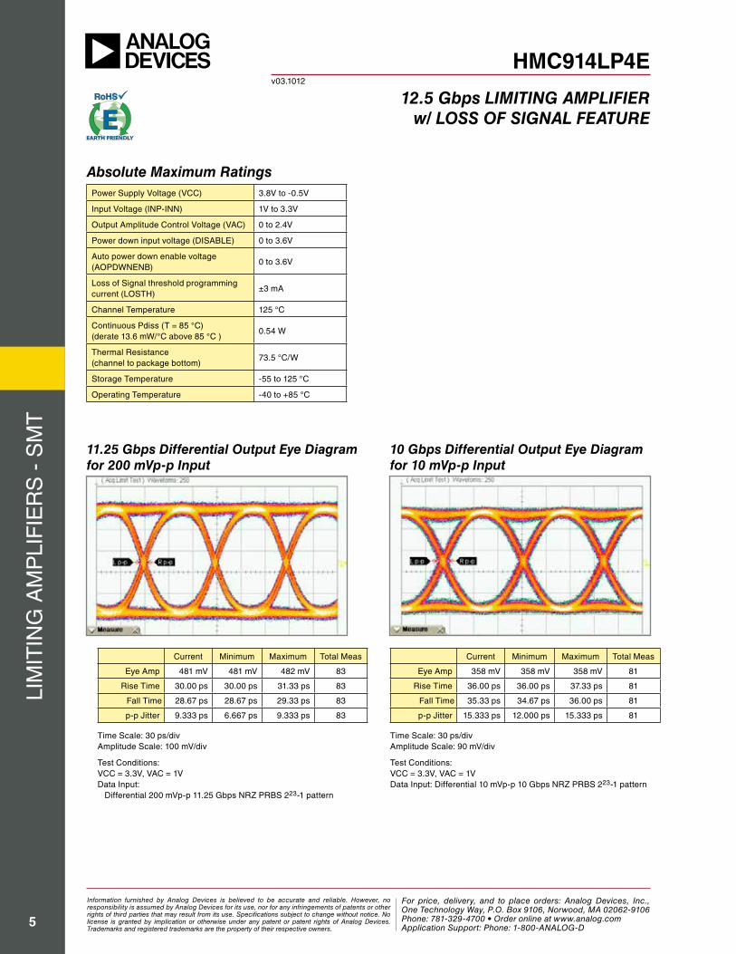
11.25 Gbps Differential Output Eye Diagramfor 200 mVp-p Input
10 Gbps Differential Output Eye Diagramfor 10 mVp-p Input
Time Scale: 30 ps/divAmplitude Scale: 100 mV/div
Test Conditions:VCC = 3.3V, VAC = 1VData Input: Differential 200 mVp-p 11.25 Gbps NRZ PRBS 223-1 pattern
Time Scale: 30 ps/divAmplitude Scale: 90 mV/div
Test Conditions:VCC = 3.3V, VAC = 1VData Input: Differential 10 mVp-p 10 Gbps NRZ PRBS 223-1 pattern
Current Minimum Maximum Total Meas
Eye Amp 481 mV 481 mV 482 mV 83
Rise Time 30.00 ps 30.00 ps 31.33 ps 83
Fall Time 28.67 ps 28.67 ps 29.33 ps 83
p-p Jitter 9.333 ps 6.667 ps 9.333 ps 83
Current Minimum Maximum Total Meas
Eye Amp 358 mV 358 mV 358 mV 81
Rise Time 36.00 ps 36.00 ps 37.33 ps 81
Fall Time 35.33 ps 34.67 ps 36.00 ps 81
p-p Jitter 15.333 ps 12.000 ps 15.333 ps 81
Power Supply Voltage (VCC) 3.8V to -0.5V
Input Voltage (INP-INN) 1V to 3.3V
Output Amplitude Control Voltage (VAC) 0 to 2.4V
Power down input voltage (DISABLE) 0 to 3.6V
Auto power down enable voltage(AOPDWNENB)
0 to 3.6V
Loss of Signal threshold programming current (LOSTH)
±3 mA
Channel Temperature 125 °C
Continuous Pdiss (T = 85 °C)(derate 13.6 mW/°C above 85 °C )
0.54 W
Thermal Resistance(channel to package bottom)
73.5 °C/W
Storage Temperature -55 to 125 °C
Operating Temperature -40 to +85 °C
Absolute Maximum Ratings
Information furnished by Analog Devices is believed to be accurate and reliable. However, no responsibility is assumed by Analog Devices for its use, nor for any infringements of patents or other rights of third parties that may result from its use. Specifications subject to change without notice. No license is granted by implication or otherwise under any patent or patent rights of Analog Devices. Trademarks and registered trademarks are the property of their respective owners.
For price, delivery, and to place orders: Analog Devices, Inc., One Technology Way, P.O. Box 9106, Norwood, MA 02062-9106 Phone: 781-329-4700 • Order online at www.analog.com Application Support: Phone: 1-800-ANALOG-D
For price, delivery and to place orders: Hittite Microwave Corporation, 2 Elizabeth Drive, Chelmsford, MA 01824Phone: 978-250-3343 Fax: 978-250-3373 Order On-line at www.hittite.com
Application Support: Phone: 978-250-3343 or [email protected]
lim
itin
g a
mp
lif
ier
s -
sm
t
6
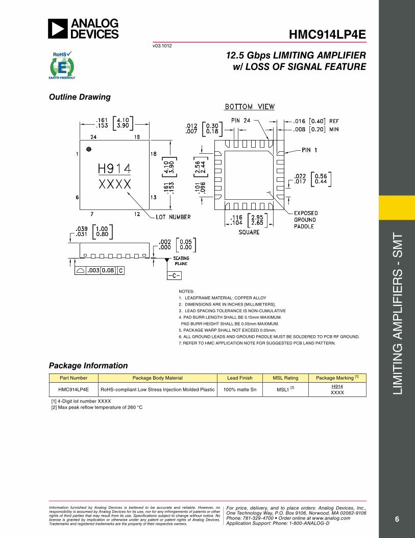
Outline Drawing
Part Number Package Body Material Lead Finish MSL Rating Package Marking [1]
HMC914LP4E RoHS-compliant Low Stress Injection Molded Plastic 100% matte Sn MSL1 [2] H914XXXX
[1] 4-Digit lot number XXXX[2] Max peak reflow temperature of 260 °C
Package Information
NOTES:
1. LEADFRAME MATERIAL: COPPER ALLOY
2. DIMENSIONS ARE IN INCHES [MILLIMETERS].
3. LEAD SPACING TOLERANCE IS NON-CUMULATIVE
4. PAD BURR LENGTH SHALL BE 0.15mm MAXIMUM.
PAD BURR HEIGHT SHALL BE 0.05mm MAXIMUM.
5. PACKAGE WARP SHALL NOT EXCEED 0.05mm.
6. ALL GROUND LEADS AND GROUND PADDLE MUST BE SOLDERED TO PCB RF GROUND.
7. REFER TO HMC APPLICATION NOTE FOR SUGGESTED PCB LAND PATTERN.
HMC914LP4Ev03.1012
12.5 Gbps LIMITING AMPLIFIERw/ LOSS OF SIGNAL FEATURE
Information furnished by Analog Devices is believed to be accurate and reliable. However, no responsibility is assumed by Analog Devices for its use, nor for any infringements of patents or other rights of third parties that may result from its use. Specifications subject to change without notice. No license is granted by implication or otherwise under any patent or patent rights of Analog Devices. Trademarks and registered trademarks are the property of their respective owners.
For price, delivery, and to place orders: Analog Devices, Inc., One Technology Way, P.O. Box 9106, Norwood, MA 02062-9106 Phone: 781-329-4700 • Order online at www.analog.com Application Support: Phone: 1-800-ANALOG-D
For price, delivery and to place orders: Hittite Microwave Corporation, 2 Elizabeth Drive, Chelmsford, MA 01824Phone: 978-250-3343 Fax: 978-250-3373 Order On-line at www.hittite.com
Application Support: Phone: 978-250-3343 or [email protected]
lim
itin
g a
mp
lif
ier
s -
sm
t
7
HMC914LP4Ev03.1012
12.5 Gbps LIMITING AMPLIFIERw/ LOSS OF SIGNAL FEATURE
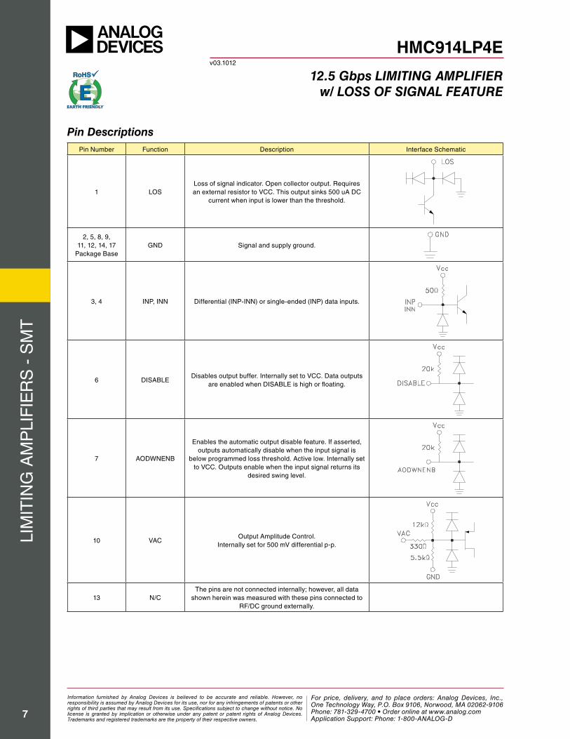
Pin Number Function Description Interface Schematic
1 LOSLoss of signal indicator. Open collector output. Requires an external resistor to VCC. This output sinks 500 uA DC
current when input is lower than the threshold.
2, 5, 8, 9, 11, 12, 14, 17
Package BaseGND Signal and supply ground.
3, 4 INP, INN Differential (INP-INN) or single-ended (INP) data inputs.
6 DISABLEDisables output buffer. Internally set to VCC. Data outputs
are enabled when DISABLE is high or floating.
7 AODWNENB
Enables the automatic output disable feature. If asserted, outputs automatically disable when the input signal is
below programmed loss threshold. Active low. Internally set to VCC. Outputs enable when the input signal returns its
desired swing level.
10 VACOutput Amplitude Control.
Internally set for 500 mV differential p-p.
13 N/CThe pins are not connected internally; however, all data
shown herein was measured with these pins connected to RF/DC ground externally.
Pin Descriptions
Information furnished by Analog Devices is believed to be accurate and reliable. However, no responsibility is assumed by Analog Devices for its use, nor for any infringements of patents or other rights of third parties that may result from its use. Specifications subject to change without notice. No license is granted by implication or otherwise under any patent or patent rights of Analog Devices. Trademarks and registered trademarks are the property of their respective owners.
For price, delivery, and to place orders: Analog Devices, Inc., One Technology Way, P.O. Box 9106, Norwood, MA 02062-9106 Phone: 781-329-4700 • Order online at www.analog.com Application Support: Phone: 1-800-ANALOG-D
For price, delivery and to place orders: Hittite Microwave Corporation, 2 Elizabeth Drive, Chelmsford, MA 01824Phone: 978-250-3343 Fax: 978-250-3373 Order On-line at www.hittite.com
Application Support: Phone: 978-250-3343 or [email protected]
lim
itin
g a
mp
lif
ier
s -
sm
t
8
Pin Descriptions (Continued)
HMC914LP4Ev03.1012
12.5 Gbps LIMITING AMPLIFIERw/ LOSS OF SIGNAL FEATURE
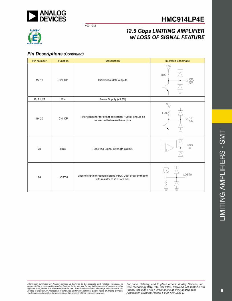
Pin Number Function Description Interface Schematic
15, 16 QN, QP Differential data outputs
18, 21, 22 Vcc Power Supply (+3.3V)
19, 20 CN, CPFilter capacitor for offset correction. 100 nF should be
connected between these pins.
23 RSSI Received Signal Strength Output.
24 LOSTHLoss of signal threshold setting input. User programmable
with resistor to VCC or GND.
Information furnished by Analog Devices is believed to be accurate and reliable. However, no responsibility is assumed by Analog Devices for its use, nor for any infringements of patents or other rights of third parties that may result from its use. Specifications subject to change without notice. No license is granted by implication or otherwise under any patent or patent rights of Analog Devices. Trademarks and registered trademarks are the property of their respective owners.
For price, delivery, and to place orders: Analog Devices, Inc., One Technology Way, P.O. Box 9106, Norwood, MA 02062-9106 Phone: 781-329-4700 • Order online at www.analog.com Application Support: Phone: 1-800-ANALOG-D
For price, delivery and to place orders: Hittite Microwave Corporation, 2 Elizabeth Drive, Chelmsford, MA 01824Phone: 978-250-3343 Fax: 978-250-3373 Order On-line at www.hittite.com
Application Support: Phone: 978-250-3343 or [email protected]
lim
itin
g a
mp
lif
ier
s -
sm
t
9
HMC914LP4Ev03.1012
12.5 Gbps LIMITING AMPLIFIERw/ LOSS OF SIGNAL FEATURE
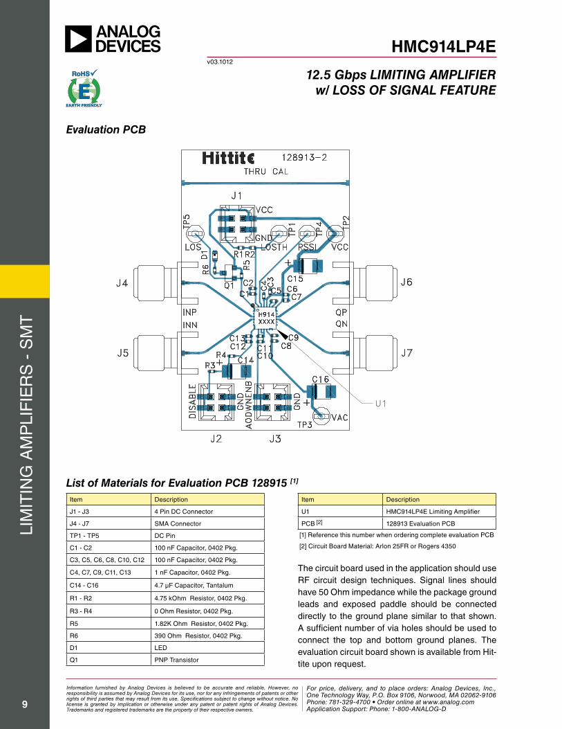
Evaluation PCB
The circuit board used in the application should use RF circuit design techniques. Signal lines should have 50 Ohm impedance while the package ground leads and exposed paddle should be connected directly to the ground plane similar to that shown. A sufficient number of via holes should be used to connect the top and bottom ground planes. The evaluation circuit board shown is available from Hit-tite upon request.
List of Materials for Evaluation PCB 128915 [1]
Item Description
J1 - J3 4 Pin DC Connector
J4 - J7 SMA Connector
TP1 - TP5 DC Pin
C1 - C2 100 nF Capacitor, 0402 Pkg.
C3, C5, C6, C8, C10, C12 100 nF Capacitor, 0402 Pkg.
C4, C7, C9, C11, C13 1 nF Capacitor, 0402 Pkg.
C14 - C16 4.7 µF Capacitor, Tantalum
R1 - R2 4.75 kOhm Resistor, 0402 Pkg.
R3 - R4 0 Ohm Resistor, 0402 Pkg.
R5 1.82K Ohm Resistor, 0402 Pkg.
R6 390 Ohm Resistor, 0402 Pkg.
D1 LED
Q1 PNP Transistor
Item Description
U1 HMC914LP4E Limiting Amplifier
PCB [2] 128913 Evaluation PCB
[1] Reference this number when ordering complete evaluation PCB
[2] Circuit Board Material: Arlon 25FR or Rogers 4350
Information furnished by Analog Devices is believed to be accurate and reliable. However, no responsibility is assumed by Analog Devices for its use, nor for any infringements of patents or other rights of third parties that may result from its use. Specifications subject to change without notice. No license is granted by implication or otherwise under any patent or patent rights of Analog Devices. Trademarks and registered trademarks are the property of their respective owners.
For price, delivery, and to place orders: Analog Devices, Inc., One Technology Way, P.O. Box 9106, Norwood, MA 02062-9106 Phone: 781-329-4700 • Order online at www.analog.com Application Support: Phone: 1-800-ANALOG-D
For price, delivery and to place orders: Hittite Microwave Corporation, 2 Elizabeth Drive, Chelmsford, MA 01824Phone: 978-250-3343 Fax: 978-250-3373 Order On-line at www.hittite.com
Application Support: Phone: 978-250-3343 or [email protected]
lim
itin
g a
mp
lif
ier
s -
sm
t
10
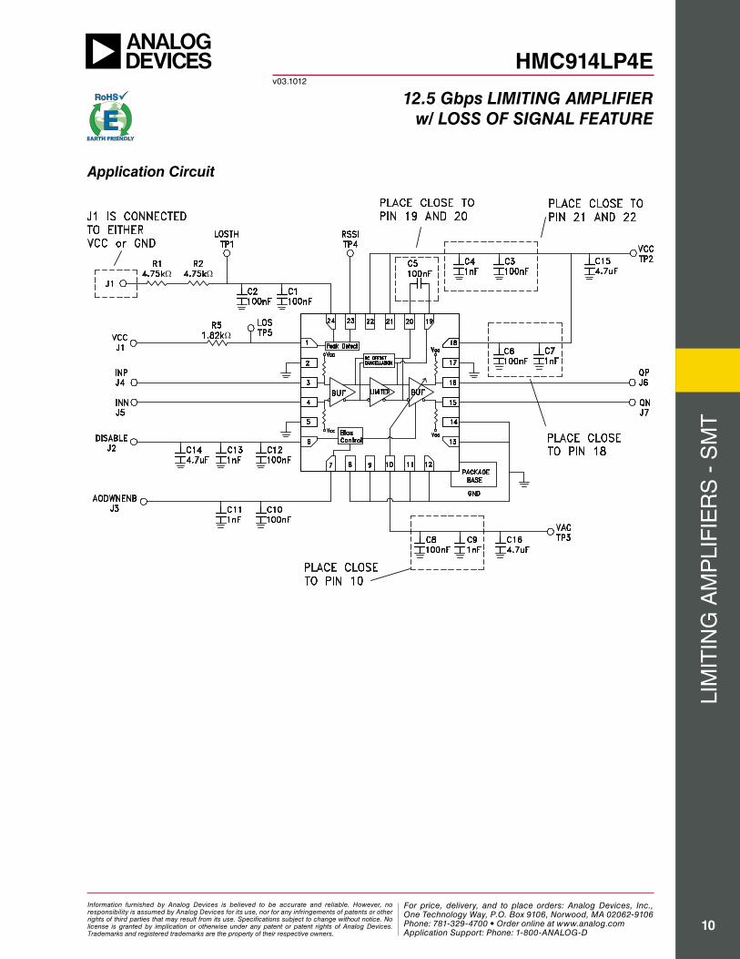
Application Circuit
HMC914LP4Ev03.1012
12.5 Gbps LIMITING AMPLIFIERw/ LOSS OF SIGNAL FEATURE
Information furnished by Analog Devices is believed to be accurate and reliable. However, no responsibility is assumed by Analog Devices for its use, nor for any infringements of patents or other rights of third parties that may result from its use. Specifications subject to change without notice. No license is granted by implication or otherwise under any patent or patent rights of Analog Devices. Trademarks and registered trademarks are the property of their respective owners.
For price, delivery, and to place orders: Analog Devices, Inc., One Technology Way, P.O. Box 9106, Norwood, MA 02062-9106 Phone: 781-329-4700 • Order online at www.analog.com Application Support: Phone: 1-800-ANALOG-D
For price, delivery and to place orders: Hittite Microwave Corporation, 2 Elizabeth Drive, Chelmsford, MA 01824Phone: 978-250-3343 Fax: 978-250-3373 Order On-line at www.hittite.com
Application Support: Phone: 978-250-3343 or [email protected]
lim
itin
g a
mp
lif
ier
s -
sm
t
11
HMC914LP4Ev03.1012
12.5 Gbps LIMITING AMPLIFIERw/ LOSS OF SIGNAL FEATURE
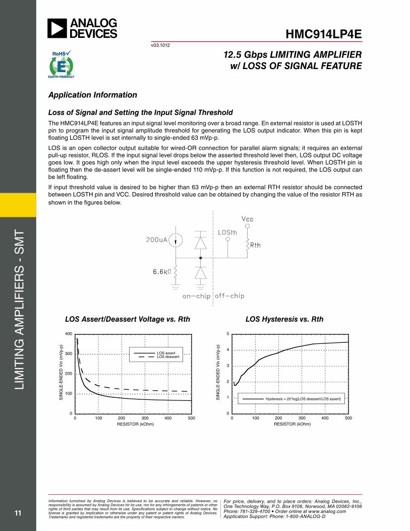
Application Information
Loss of Signal and Setting the Input Signal ThresholdThe HMC914LP4E features an input signal level monitoring over a broad range. En external resistor is used at LOSTH pin to program the input signal amplitude threshold for generating the LOS output indicator. When this pin is kept floating LOSTH level is set internally to single-ended 63 mVp-p.
LOS is an open collector output suitable for wired-OR connection for parallel alarm signals; it requires an external pull-up resistor, RLOS. If the input signal level drops below the asserted threshold level then, LOS output DC voltage goes low. It goes high only when the input level exceeds the upper hysteresis threshold level. When LOSTH pin is floating then the de-assert level will be single-ended 110 mVp-p. If this function is not required, the LOS output can be left floating.
If input threshold value is desired to be higher than 63 mVp-p then an external RTH resistor should be connected between LOSTH pin and VCC. Desired threshold value can be obtained by changing the value of the resistor RTH as shown in the figures below.
LOS Assert/Deassert Voltage vs. Rth LOS Hysteresis vs. Rth
0
100
200
300
400
0 100 200 300 400 500
LOS assertLOS deassert
RESISTOR (kOhm)
SIN
GLE
-EN
DE
D V
in (
mV
p-p)
0
1
2
3
4
5
0 100 200 300 400 500
Hysteresis = 20*log{LOS deassert/LOS assert}
RESISTOR (kOhm)
SIN
GLE
-EN
DE
D V
in (
mV
p-p)
Information furnished by Analog Devices is believed to be accurate and reliable. However, no responsibility is assumed by Analog Devices for its use, nor for any infringements of patents or other rights of third parties that may result from its use. Specifications subject to change without notice. No license is granted by implication or otherwise under any patent or patent rights of Analog Devices. Trademarks and registered trademarks are the property of their respective owners.
For price, delivery, and to place orders: Analog Devices, Inc., One Technology Way, P.O. Box 9106, Norwood, MA 02062-9106 Phone: 781-329-4700 • Order online at www.analog.com Application Support: Phone: 1-800-ANALOG-D
For price, delivery and to place orders: Hittite Microwave Corporation, 2 Elizabeth Drive, Chelmsford, MA 01824Phone: 978-250-3343 Fax: 978-250-3373 Order On-line at www.hittite.com
Application Support: Phone: 978-250-3343 or [email protected]
lim
itin
g a
mp
lif
ier
s -
sm
t
12
HMC914LP4Ev03.1012
12.5 Gbps LIMITING AMPLIFIERw/ LOSS OF SIGNAL FEATURE
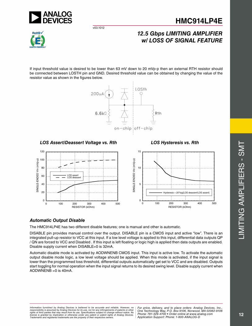
If input threshold value is desired to be lower than 63 mV down to 20 mVp-p then an external RTH resistor should be connected between LOSTH pin and GND. Desired threshold value can be obtained by changing the value of the resistor value as shown in the figures below.
LOS Assert/Deassert Voltage vs. Rth LOS Hysteresis vs. Rth
0
20
40
60
80
100
120
0 100 200 300 400 500
LOS assertLOS deassert
RESISTOR (kOhm)
SIN
GLE
-EN
DE
D V
in (
mV
p-p)
0
5
10
15
0 100 200 300 400 500
Hysteresis = 20*log{LOS deassert/LOS assert}
RESISTOR (kOhm)
SIN
GLE
-EN
DE
D V
in (
mV
p-p)
Automatic Output DisableThe HMC914LP4E has two different disable features; one is manual and other is automatic.
DISABLE pin provides manual control over the output. DISABLE pin is a CMOS input and active “low”. There is an integrated pull-up resistor to VCC at this input. If a low level voltage is applied to this input, differential data outputs QP / QN are forced to VCC and Disabled . If this input is left floating or logic high is applied then data outputs are enabled. Disable supply current when DISABLE=0 is 32mA.
Automatic disable mode is activated by AODWNENB CMOS input. This input is active low. To activate the automatic output disable mode logic, a low level voltage should be applied. When this mode is activated, if the input signal is lower than the programmed loss threshold, differential outputs automatically get set to VCC and are disabled. Outputs start toggling for normal operation when the input signal returns to its desired swing level. Disable supply current when AODWNENB =0 is 40mA.
Information furnished by Analog Devices is believed to be accurate and reliable. However, no responsibility is assumed by Analog Devices for its use, nor for any infringements of patents or other rights of third parties that may result from its use. Specifications subject to change without notice. No license is granted by implication or otherwise under any patent or patent rights of Analog Devices. Trademarks and registered trademarks are the property of their respective owners.
For price, delivery, and to place orders: Analog Devices, Inc., One Technology Way, P.O. Box 9106, Norwood, MA 02062-9106 Phone: 781-329-4700 • Order online at www.analog.com Application Support: Phone: 1-800-ANALOG-D


![INDEX [link.springer.com]978-0-306-48134-5/1.pdf · 314 PHILOSOPHY, PSYCHOLOGY, AND PSYCHOLOGISM anthropological logic, 85, 86, 88 anthropomorphism, 171, 250 anti-descriptivism, 54;](https://img.pdfslide.us/doc/110x75/5c6bf20609d3f2a1458c2a2e/index-link-978-0-306-48134-51pdf-314-philosophy-psychology-and-psychologism.jpg)