Embed Size (px)
Citation preview
For price, delivery and to place orders: Hittite Microwave Corporation, 2 Elizabeth Drive, Chelmsford, MA 01824Phone: 978-250-3343 Fax: 978-250-3373 Order On-line at www.hittite.com
Application Support: Phone: 978-250-3343 or [email protected]
FIL
TE
RS
- T
UN
AB
LE -
SM
T
1
HMC895LP4Ev01.0911
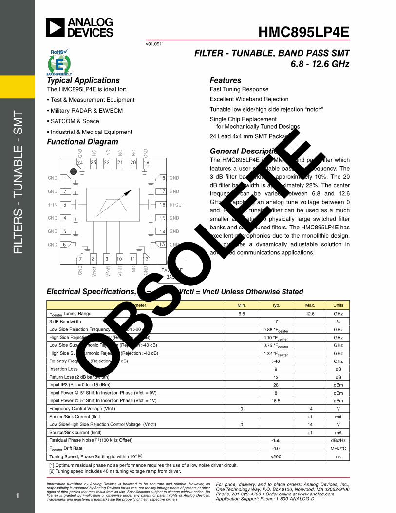
FILTER - TUNABLE, BAND PASS SMT6.8 - 12.6 GHz
Functional Diagram
The HMC895LP4E is a MMIC band pass filter which features a user selectable passband frequency. The 3 dB filter bandwidth is approximately 10%. The 20 dB filter bandwidth is approximately 22%. The center frequency can be varied between 6.8 and 12.6 GHz by applying an analog tune voltage between 0 and 14V. This tunable filter can be used as a much smaller alternative to physically large switched filter banks and cavity tuned filters. The HMC895LP4E has excellent microphonics due to the monolithic design, and provides a dynamically adjustable solution in advanced communications applications.
Typical Applications Features
General Description
The HMC895LP4E is ideal for:
• Test & Measurement Equipment
• Military RADAR & EW/ECM
• SATCOM & Space
• Industrial & Medical Equipment
Fast Tuning Response
Excellent Wideband Rejection
Tunable low side/high side rejection “notch”
Single Chip Replacement for Mechanically Tuned Designs
24 Lead 4x4 mm SMT Package
Electrical Specifications, TA = +25 °C, Vfctl = Vnctl Unless Otherwise Stated
Parameter Min. Typ. Max. Units
Fcenter Tuning Range 6.8 12.6 GHz
3 dB Bandwidth 10 %
Low Side Rejection Frequency (Rejection >20 dB) 0.88 *Fcenter GHz
High Side Rejection Frequency (Rejection >20 dB) 1.10 *Fcenter GHz
Low Side Sub-Harmonic Rejection (Rejection >40 dB) 0.75 *Fcenter GHz
High Side Sub-Harmonic Rejection (Rejection >40 dB) 1.22 *Fcenter GHz
Re-entry Frequency (Rejection <30 dB) >40 GHz
Insertion Loss 9 dB
Return Loss (2 dB bandwidth) 12 dB
Input IP3 (Pin = 0 to +15 dBm) 28 dBm
Input Power @ 5° Shift In Insertion Phase (Vfctl = 0V) 8 dBm
Input Power @ 5° Shift In Insertion Phase (Vfctl = 1V) 16.5 dBm
Frequency Control Voltage (Vfctl) 0 14 V
Source/Sink Current (Ifctl ±1 mA
Low Side/High Side Rejection Control Voltage (Vnctl) 0 14 V
Source/Sink current (Inctl) ±1 mA
Residual Phase Noise [1] (100 kHz Offset) -155 dBc/Hz
Fcenter Drift Rate -1.0 MHz/°C
Tuning Speed, Phase Settling to within 10° [2] <200 ns
[1] Optimum residual phase noise performance requires the use of a low noise driver circuit.[2] Tuning speed includes 40 ns tuning voltage ramp from driver.
OBSOLETE
Information furnished by Analog Devices is believed to be accurate and reliable. However, no responsibility is assumed by Analog Devices for its use, nor for any infringements of patents or other rights of third parties that may result from its use. Specifications subject to change without notice. No license is granted by implication or otherwise under any patent or patent rights of Analog Devices. Trademarks and registered trademarks are the property of their respective owners.
For price, delivery, and to place orders: Analog Devices, Inc., One Technology Way, P.O. Box 9106, Norwood, MA 02062-9106 Phone: 781-329-4700 • Order online at www.analog.com Application Support: Phone: 1-800-ANALOG-D
For price, delivery and to place orders: Hittite Microwave Corporation, 2 Elizabeth Drive, Chelmsford, MA 01824Phone: 978-250-3343 Fax: 978-250-3373 Order On-line at www.hittite.com
Application Support: Phone: 978-250-3343 or [email protected]
FIL
TE
RS
- T
UN
AB
LE -
SM
T
2
HMC895LP4Ev01.0911
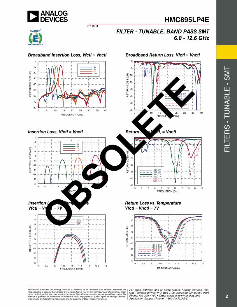
FILTER - TUNABLE, BAND PASS SMT6.8 - 12.6 GHz
Broadband Insertion Loss, Vfctl = Vnctl
Insertion Loss, Vfctl = Vnctl
Insertion Loss vs. Temperature Vfctl = Vnctl = 7V
Broadband Return Loss, Vfctl = Vnctl
Return Loss Vfctl, = Vnctl
Return Loss vs. Temperature Vfctl = Vnctl = 7V
-80
-70
-60
-50
-40
-30
-20
-10
0
0 5 10 15 20 25 30 35 40
0V3V7V14V
INS
ER
TIO
N L
OS
S (
dB)
FREQUENCY (GHz)
-35
-30
-25
-20
-15
-10
-5
0
0 5 10 15 20 25 30 35 40
S11_0VS22_0VS11_7VS22_7VS11_14VS22_14V
RE
TU
RN
LO
SS
(dB
)
FREQUENCY (GHz)
-20
-18
-16
-14
-12
-10
-8
-6
-4
-2
0
5 6 7 8 9 10 11 12 13 14 15
0V3V7V14V
INS
ER
TIO
N L
OS
S (
dB)
FREQUENCY (GHz)
-35
-30
-25
-20
-15
-10
-5
0
5 6 7 8 9 10 11 12 13 14 15
S11_0VS22_0VS11_7VS22_7VS11_14VS22_14V
RE
TU
RN
LO
SS
(dB
)
FREQUENCY (GHz)
-20
-18
-16
-14
-12
-10
-8
-6
-4
-2
0
9 9.5 10 10.5 11 11.5 12 12.5 13
+25C+85C-40C
INS
ER
TIO
N L
OS
S (
dB
)
FREQUENCY (GHz)
-40
-35
-30
-25
-20
-15
-10
-5
0
9 9.5 10 10.5 11 11.5 12 12.5 13
+25C_S11+25C_S22+85C_S11+85C_S22-40C_S11-40C_S22
RE
TU
RN
LO
SS
(dB
)
FREQUENCY (GHz)
OBSOLETE
Information furnished by Analog Devices is believed to be accurate and reliable. However, no responsibility is assumed by Analog Devices for its use, nor for any infringements of patents or other rights of third parties that may result from its use. Specifications subject to change without notice. No license is granted by implication or otherwise under any patent or patent rights of Analog Devices. Trademarks and registered trademarks are the property of their respective owners.
For price, delivery, and to place orders: Analog Devices, Inc., One Technology Way, P.O. Box 9106, Norwood, MA 02062-9106 Phone: 781-329-4700 • Order online at www.analog.com Application Support: Phone: 1-800-ANALOG-D
For price, delivery and to place orders: Hittite Microwave Corporation, 2 Elizabeth Drive, Chelmsford, MA 01824Phone: 978-250-3343 Fax: 978-250-3373 Order On-line at www.hittite.com
Application Support: Phone: 978-250-3343 or [email protected]
FIL
TE
RS
- T
UN
AB
LE -
SM
T
3
HMC895LP4Ev01.0911
FILTER - TUNABLE, BAND PASS SMT6.8 - 12.6 GHz
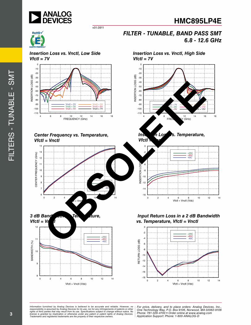
Center Frequency vs. Temperature,Vfctl = Vnctl
Insertion Loss vs. Temperature,Vfctl = Vnctl
Input Return Loss in a 2 dB Bandwidth vs. Temperature, Vfctl = Vnctl
3 dB Bandwidth vs. Temperature,Vfctl = Vnctl
6
7
8
9
10
11
12
13
14
0 2 4 6 8 10 12 14
+25C+85C -40C
CE
NT
ER
FR
EQ
UE
NC
Y (
GH
z)
Vfctl = Vnctl (Vdc)
-16
-14
-12
-10
-8
-6
-4
-2
0
0 2 4 6 8 10 12 14
+25C+85C-40C
INS
ER
TIO
N L
OS
S (
dB)
Vfctl = Vnctl (Vdc)
8
9
10
11
12
0 2 4 6 8 10 12 14
+25C+85C -40C
BA
ND
WID
TH
(%
)
Vfctl = Vnctl (Vdc)
-18
-16
-14
-12
-10
-8
-6
-4
-2
0
0 2 4 6 8 10 12 14
+25C+85C -40C
RE
TU
RN
LO
SS
(dB
)
Vfctl = Vnctl (Vdc)
Insertion Loss vs. Vnctl, Low SideVfctl = 7V
Insertion Loss vs. Vnctl, High SideVfctl = 7V
-110
-100
-90
-80
-70
-60
-50
-40
-30
-20
-10
0
4 6 8 10 12 14 16 18
Vnctl = 2VVnctl = 3VVnctl = 4V
Vnctl = 5VVnctl = 6VVnctl = 7V
INS
ER
TIO
N L
OS
S (
dB)
FREQUENCY (GHz)
-110
-100
-90
-80
-70
-60
-50
-40
-30
-20
-10
0
4 6 8 10 12 14 16 18
Vnctl = 7VVnctl = 8VVnctl = 9V
Vnctl = 10VVnctl = 11VVnctl = 12V
INS
ER
TIO
N L
OS
S (
dB)
FREQUENCY (GHz)
OBSOLETE
Information furnished by Analog Devices is believed to be accurate and reliable. However, no responsibility is assumed by Analog Devices for its use, nor for any infringements of patents or other rights of third parties that may result from its use. Specifications subject to change without notice. No license is granted by implication or otherwise under any patent or patent rights of Analog Devices. Trademarks and registered trademarks are the property of their respective owners.
For price, delivery, and to place orders: Analog Devices, Inc., One Technology Way, P.O. Box 9106, Norwood, MA 02062-9106 Phone: 781-329-4700 • Order online at www.analog.com Application Support: Phone: 1-800-ANALOG-D
For price, delivery and to place orders: Hittite Microwave Corporation, 2 Elizabeth Drive, Chelmsford, MA 01824Phone: 978-250-3343 Fax: 978-250-3373 Order On-line at www.hittite.com
Application Support: Phone: 978-250-3343 or [email protected]
FIL
TE
RS
- T
UN
AB
LE -
SM
T
4
HMC895LP4Ev01.0911
FILTER - TUNABLE, BAND PASS SMT6.8 - 12.6 GHz
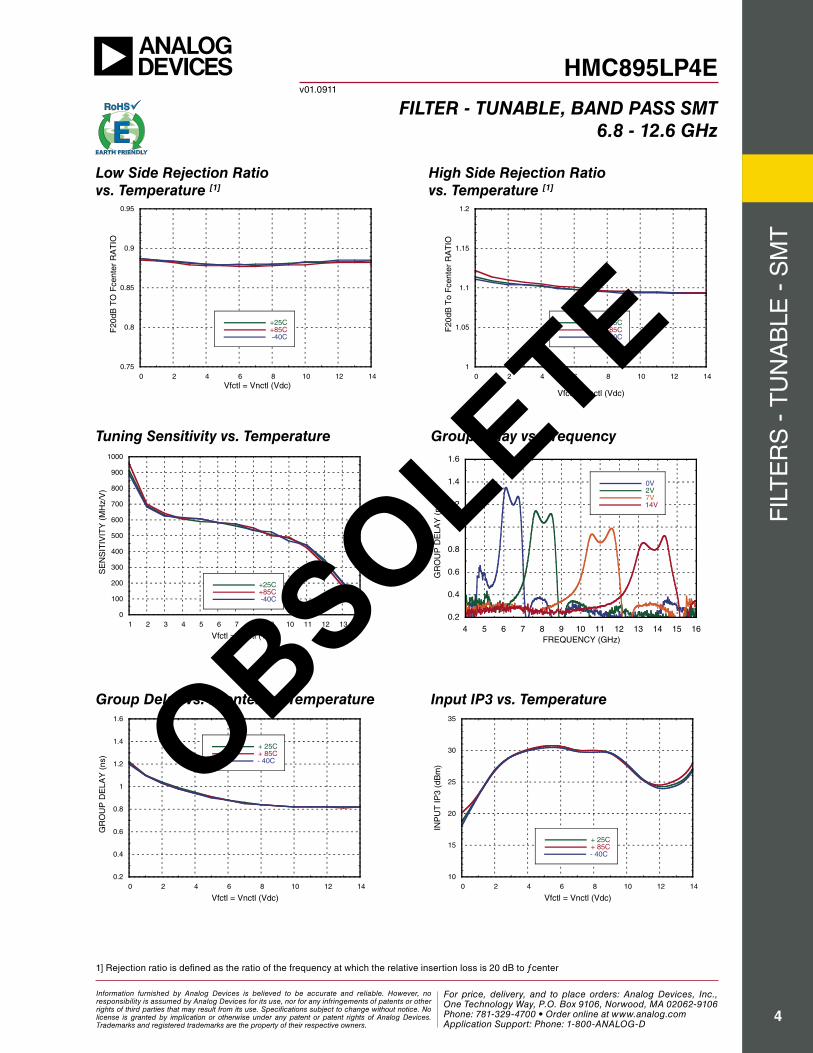
Tuning Sensitivity vs. Temperature
Group Delay vs. Fcenter vs. Temperature Input IP3 vs. Temperature
Group Delay vs. Frequency
Low Side Rejection Ratio vs. Temperature [1]
High Side Rejection Ratio vs. Temperature [1]
0.75
0.8
0.85
0.9
0.95
0 2 4 6 8 10 12 14
+25C+85C -40C
F20
dB T
O F
cent
er R
AT
IO
Vfctl = Vnctl (Vdc)
1
1.05
1.1
1.15
1.2
0 2 4 6 8 10 12 14
+25C+85C -40C
F20
dB T
o F
cent
er R
AT
IO
Vfctl = Vnctl (Vdc)
0
100
200
300
400
500
600
700
800
900
1000
1 2 3 4 5 6 7 8 9 10 11 12 13 14
+25C+85C -40C
SE
NS
ITIV
ITY
(M
Hz/
V)
Vfctl = Vnctl (Vdc)
0.2
0.4
0.6
0.8
1
1.2
1.4
1.6
4 5 6 7 8 9 10 11 12 13 14 15 16
0V2V7V14V
FREQUENCY (GHz)
GR
OU
P D
ELA
Y (
ns)
0.2
0.4
0.6
0.8
1
1.2
1.4
1.6
0 2 4 6 8 10 12 14
+ 25C+ 85C- 40C
GR
OU
P D
ELA
Y (
ns)
Vfctl = Vnctl (Vdc)
10
15
20
25
30
35
0 2 4 6 8 10 12 14
+ 25C+ 85C- 40C
INP
UT
IP3
(dB
m)
Vfctl = Vnctl (Vdc)
1] Rejection ratio is defined as the ratio of the frequency at which the relative insertion loss is 20 dB to ƒcenter
OBSOLETE
Information furnished by Analog Devices is believed to be accurate and reliable. However, no responsibility is assumed by Analog Devices for its use, nor for any infringements of patents or other rights of third parties that may result from its use. Specifications subject to change without notice. No license is granted by implication or otherwise under any patent or patent rights of Analog Devices. Trademarks and registered trademarks are the property of their respective owners.
For price, delivery, and to place orders: Analog Devices, Inc., One Technology Way, P.O. Box 9106, Norwood, MA 02062-9106 Phone: 781-329-4700 • Order online at www.analog.com Application Support: Phone: 1-800-ANALOG-D
For price, delivery and to place orders: Hittite Microwave Corporation, 2 Elizabeth Drive, Chelmsford, MA 01824Phone: 978-250-3343 Fax: 978-250-3373 Order On-line at www.hittite.com
Application Support: Phone: 978-250-3343 or [email protected]
FIL
TE
RS
- T
UN
AB
LE -
SM
T
5
HMC895LP4Ev01.0911
FILTER - TUNABLE, BAND PASS SMT6.8 - 12.6 GHz
ELECTROSTATIC SENSITIVE DEVICEOBSERVE HANDLING PRECAUTIONS
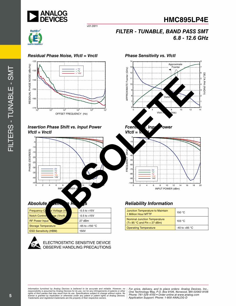
Absolute Maximum Ratings Reliability InformationFrequency Control Voltage (Vfctl) -0.5 to +15V
Notch Control Voltage (Vnctl) -0.5 to +15V
RF Power Input 27 dBm
Storage Temperature -65 to +150 °C
ESD Sensitivity (HBM) 150V
Junction Temperature to Maintain 1 Million Hour MTTF
150 °C
Nominal Junction Temperature (T= 85 °C and Pin = 27 dBm)
103 °C
Operating Temperature -40 to +85 °C
Fcenter vs. Input PowerVfctl = Vnctl
Insertion Phase Shift vs. Input PowerVfctl = Vnctl
-45
-40
-35
-30
-25
-20
-15
-10
-5
0
0 2 4 6 8 10 12 14 16 18 20
0V1V7V10v14V
PH
AS
E (
DE
GR
EE
S)
INPUT POWER (dBm)
-100
-90
-80
-70
-60
-50
-40
-30
-20
-10
0
0 2 4 6 8 10 12 14 16 18 20
0V1V7V10V14V
FR
EQ
UE
NC
Y (
MH
z)
INPUT POWER (dBm)
Phase Sensitivity vs. VfctlResidual Phase Noise, Vfctl = Vnctl
-170
-160
-150
-140
-130
-120
102 103 104 105 106 107
+ 1V+ 7V+ 14V
RE
SID
UA
L P
HA
SE
NO
ISE
(dB
c/H
z)
OFFSET FREQUENCY (Hz)
6
7
8
9
10
11
12
13
14
0
1
2
3
4
5
6
7
8
0 2 4 6 8 10 12 14
AP
PR
OX
IMA
TE
Fce
nter
(G
Hz)
DE
LTA
PH
I (RA
D/V
)
Vfctl = Vnctl (Vdc)
Delta Phi
Approximate Fcenter
OBSOLETE
Information furnished by Analog Devices is believed to be accurate and reliable. However, no responsibility is assumed by Analog Devices for its use, nor for any infringements of patents or other rights of third parties that may result from its use. Specifications subject to change without notice. No license is granted by implication or otherwise under any patent or patent rights of Analog Devices. Trademarks and registered trademarks are the property of their respective owners.
For price, delivery, and to place orders: Analog Devices, Inc., One Technology Way, P.O. Box 9106, Norwood, MA 02062-9106 Phone: 781-329-4700 • Order online at www.analog.com Application Support: Phone: 1-800-ANALOG-D
For price, delivery and to place orders: Hittite Microwave Corporation, 2 Elizabeth Drive, Chelmsford, MA 01824Phone: 978-250-3343 Fax: 978-250-3373 Order On-line at www.hittite.com
Application Support: Phone: 978-250-3343 or [email protected]
FIL
TE
RS
- T
UN
AB
LE -
SM
T
6
HMC895LP4Ev01.0911
FILTER - TUNABLE, BAND PASS SMT6.8 - 12.6 GHz
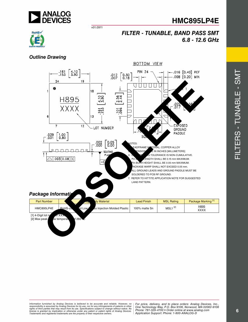
Outline Drawing
NOTES:
1. LEADFRAME MATERIAL: COPPER ALLOY
2. DIMENSIONS ARE IN INCHES [MILLIMETERS]
3. LEAD SPACING TOLERANCE IS NON-CUMULATIVE.
4. Pin BURR LENGTH SHALL BE 0.15 mm MAXIMUM.
Pin BURR HEIGHT SHALL BE 0.05 mm MAXIMUM.
5. PACKAGE WARP SHALL NOT EXCEED 0.05 mm.
6. ALL GROUND LEADS AND GROUND PADDLE MUST BE
SOLDERED TO PCB RF GROUND.
7. REFER TO HITTITE APPLICATION NOTE FOR SUGGESTED
LAND PATTERN.
Part Number Package Body Material Lead Finish MSL Rating Package Marking [1]
HMC895LP4E RoHS-compliant Low Stress Injection Molded Plastic 100% matte Sn MSL1 [2] H895XXXX
[1] 4-Digit lot number XXXX[2] Max peak reflow temperature of 260 °C
Package Information
OBSOLETE
Information furnished by Analog Devices is believed to be accurate and reliable. However, no responsibility is assumed by Analog Devices for its use, nor for any infringements of patents or other rights of third parties that may result from its use. Specifications subject to change without notice. No license is granted by implication or otherwise under any patent or patent rights of Analog Devices. Trademarks and registered trademarks are the property of their respective owners.
For price, delivery, and to place orders: Analog Devices, Inc., One Technology Way, P.O. Box 9106, Norwood, MA 02062-9106 Phone: 781-329-4700 • Order online at www.analog.com Application Support: Phone: 1-800-ANALOG-D
For price, delivery and to place orders: Hittite Microwave Corporation, 2 Elizabeth Drive, Chelmsford, MA 01824Phone: 978-250-3343 Fax: 978-250-3373 Order On-line at www.hittite.com
Application Support: Phone: 978-250-3343 or [email protected]
FIL
TE
RS
- T
UN
AB
LE -
SM
T
7
HMC895LP4Ev01.0911
FILTER - TUNABLE, BAND PASS SMT6.8 - 12.6 GHz
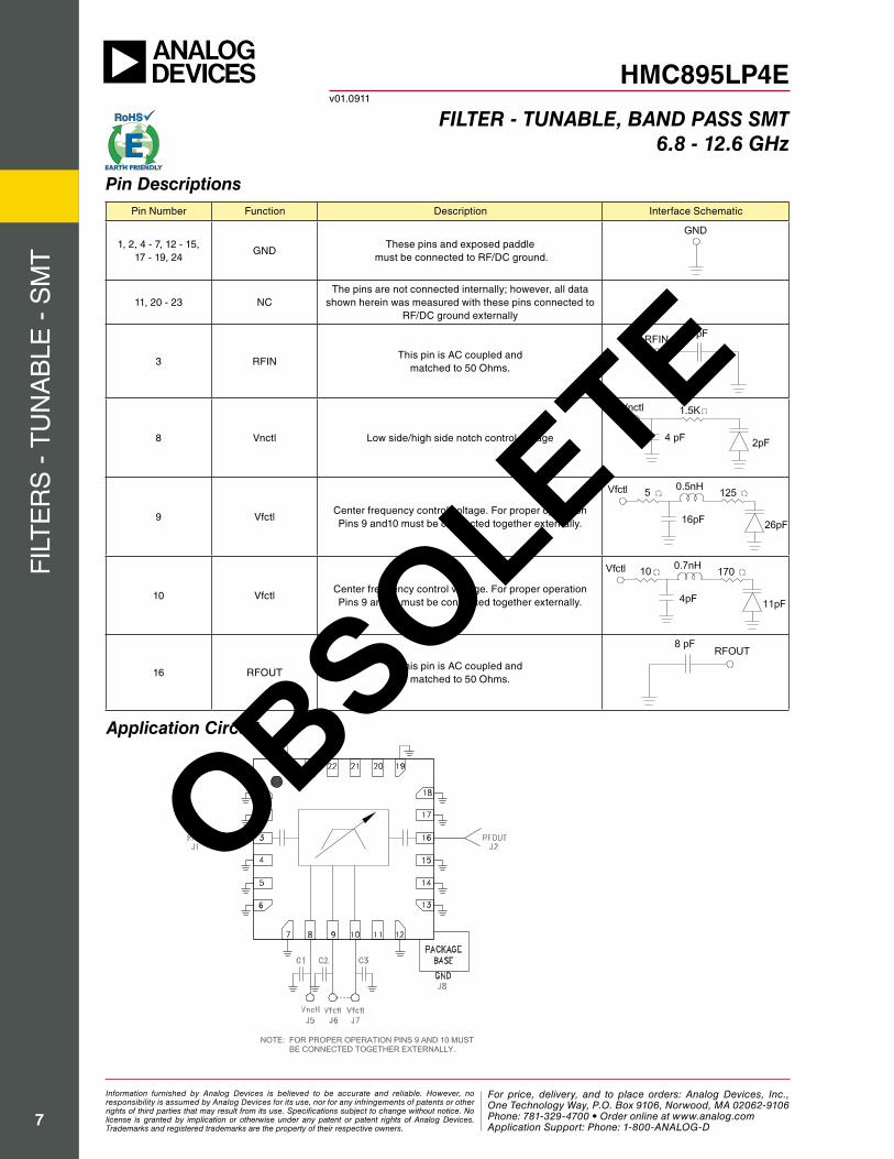
Pin Descriptions
Application Circuit
Pin Number Function Description Interface Schematic
1, 2, 4 - 7, 12 - 15, 17 - 19, 24
GNDThese pins and exposed paddle
must be connected to RF/DC ground.
11, 20 - 23 NCThe pins are not connected internally; however, all data
shown herein was measured with these pins connected toRF/DC ground externally
3 RFINThis pin is AC coupled and
matched to 50 Ohms.
8 Vnctl Low side/high side notch control voltage
9 VfctlCenter frequency control voltage. For proper operationPins 9 and10 must be connected together externally.
10 VfctlCenter frequency control voltage. For proper operationPins 9 and10 must be connected together externally.
16 RFOUTThis pin is AC coupled and
matched to 50 Ohms.
OBSOLETE
Information furnished by Analog Devices is believed to be accurate and reliable. However, no responsibility is assumed by Analog Devices for its use, nor for any infringements of patents or other rights of third parties that may result from its use. Specifications subject to change without notice. No license is granted by implication or otherwise under any patent or patent rights of Analog Devices. Trademarks and registered trademarks are the property of their respective owners.
For price, delivery, and to place orders: Analog Devices, Inc., One Technology Way, P.O. Box 9106, Norwood, MA 02062-9106 Phone: 781-329-4700 • Order online at www.analog.com Application Support: Phone: 1-800-ANALOG-D
For price, delivery and to place orders: Hittite Microwave Corporation, 2 Elizabeth Drive, Chelmsford, MA 01824Phone: 978-250-3343 Fax: 978-250-3373 Order On-line at www.hittite.com
Application Support: Phone: 978-250-3343 or [email protected]
FIL
TE
RS
- T
UN
AB
LE -
SM
T
8
HMC895LP4Ev01.0911
FILTER - TUNABLE, BAND PASS SMT6.8 - 12.6 GHz
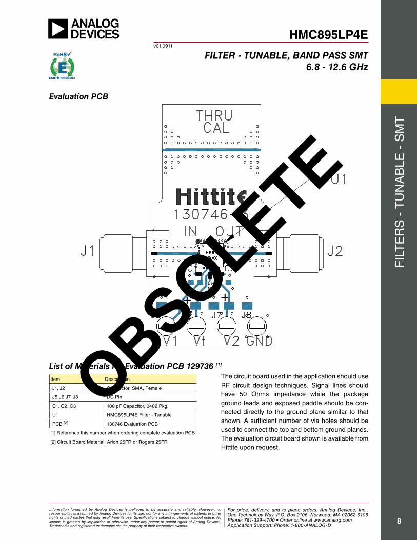
Evaluation PCB
The circuit board used in the application should use RF circuit design techniques. Signal lines should have 50 Ohms impedance while the package ground leads and exposed paddle should be con-nected directly to the ground plane similar to that shown. A sufficient number of via holes should be used to connect the top and bottom ground planes. The evaluation circuit board shown is available from Hittite upon request.
List of Materials for Evaluation PCB 129736 [1]
Item Description
J1, J2 Connector, SMA, Female
J5,J6,J7, J8 DC Pin
C1, C2, C3 100 pF Capacitor, 0402 Pkg.
U1 HMC895LP4E Filter - Tunable
PCB [2] 130746 Evaluation PCB
[1] Reference this number when ordering complete evaluation PCB
[2] Circuit Board Material: Arlon 25FR or Rogers 25FR
OBSOLETE
Information furnished by Analog Devices is believed to be accurate and reliable. However, no responsibility is assumed by Analog Devices for its use, nor for any infringements of patents or other rights of third parties that may result from its use. Specifications subject to change without notice. No license is granted by implication or otherwise under any patent or patent rights of Analog Devices. Trademarks and registered trademarks are the property of their respective owners.
For price, delivery, and to place orders: Analog Devices, Inc., One Technology Way, P.O. Box 9106, Norwood, MA 02062-9106 Phone: 781-329-4700 • Order online at www.analog.com Application Support: Phone: 1-800-ANALOG-D