Embed Size (px)
Citation preview
MO
DS
& D
EM
OD
ULA
TO
RS
- S
MT
11
1
For price, delivery and to place orders: Hittite Microwave Corporation, 2 Elizabeth Drive, Chelmsford, MA 01824Phone: 978-250-3343 Fax: 978-250-3373 Order On-line at www.hittite.com
Application Support: Phone: 978-250-3343 or [email protected]
v03.0812
WIDEBAND DIRECT QUADRATUREMODULATOR, 100 - 6000 MHz
HMC1097LP4E
General Description
Features
Functional Diagram
Typical Applications
Electrical Specifications, See Test Conditions on following page herein.
Parameter Typ. Typ. Typ. Typ. Typ. Units
Frequency Range, RF 450-960 1700-2200 2200-2700 3400-4000 5000-6000 MHz
Output Power 1.5 2.7 2.7 0 -5.2 dBm
Conversion Voltage Gain -4.7 -3.5 -3.5 -6.2 -11.4 dB
Output P1dB +11 +11 +10.5 +10 +5.3 dBm
Output Noise Floor -162 -160 -159 -159 -156 dBm/Hz
Output IP3 +29 +31 +29 +22 +17 dBm
Carrier Feedthrough (uncalibrated)
-40 -39 -36 -29 -33 dBm
Sideband Suppression (uncalibrated)
40 46 48 32 29 dBc
LO Port Return Loss 4 6 6 6 6 dB
RF Port Return Loss 12 14 15 16 16 dB
The HMC1097LP4E is a low noise, high linearity Direct Quadrature Modulator RFIC which is ideal for digital modulation applications from 0.1 to 6.0 GHz including; Cellular/3G, WiMAX/4G, Broadband Wireless Access & ISM circuits. Housed in a compact 4x4 mm (LP4) SMT QFN package, the RFIC requires minimal external components & provides a low cost alternative to more complicated double upconversion architectures. The RF output port is single-ended and matched to 50 Ohms with no external components. The LO requires -6 to +6 dBm and can be driven in either differential or single-ended mode. This device is optimized for a +5V supply, and offers improved carrier feedthrough and sideband suppression characteristics.
Very Low Noise Floor, -160 dBm/Hz
Excellent Carrier & Sideband Suppression
Very High Linearity, +30 dBm OIP3
High Output Power, +11 dBm Output P1dB
High Modulation Accuracy
24 Lead 4x4 mm QFN Package: 16 mm2
The HMC1097LP4E is Ideal for:
• UMTS, GSM or CDMA Basestations
• Fixed Wireless or WLL
• ISM Transceivers, 900 & 2400 MHz
• GMSK, QPSK, QAM, SSB Modulators
• Cellular/3G and WiMAX/4G
Information furnished by Analog Devices is believed to be accurate and reliable. However, no responsibility is assumed by Analog Devices for its use, nor for any infringements of patents or other rights of third parties that may result from its use. Specifications subject to change without notice. No license is granted by implication or otherwise under any patent or patent rights of Analog Devices. Trademarks and registered trademarks are the property of their respective owners.
For price, delivery, and to place orders: Analog Devices, Inc., One Technology Way, P.O. Box 9106, Norwood, MA 02062-9106 Phone: 781-329-4700 • Order online at www.analog.com Application Support: Phone: 1-800-ANALOG-D
MO
DS
& D
EM
OD
ULA
TO
RS
- S
MT
2
For price, delivery and to place orders: Hittite Microwave Corporation, 2 Elizabeth Drive, Chelmsford, MA 01824Phone: 978-250-3343 Fax: 978-250-3373 Order On-line at www.hittite.com
Application Support: Phone: 978-250-3343 or [email protected]
v03.0812
WIDEBAND DIRECT QUADRATUREMODULATOR, 100 - 6000 MHz
HMC1097LP4E
Electrical Specifications, (continued)
Parameter Conditions Min. Typ. Max. Units
RF Output
RF Frequency Range 100 6000 MHz
RF Return Loss 15 dB
LO Input
LO Frequency Range 100 6000 MHz
LO Input Power -6 0 +6 dBm
LO Port Return Loss 6 dB
Baseband Input Port
Baseband Input DC Voltage (Vbbdc) +0.45 (+0.4-+0.5) V
Baseband Input DC Bias Current (Ibbdc) Single-ended. 110 pA
Single-ended Baseband Input Capacitance De-embed to the lead of the device. 4.5 pF
DC Power Supply
Supply Voltage (Vcc1, Vcc2) +4.75 +5.0 +5.25 V
Supply Current (Icc1 + Icc2) EN Low 170 mA
Supply Current (Icc1 + Icc2) EN High 8 mA
Enable/Disable Interface
EN High Level Device disabled 2.2 5 V
EN Low Level Device enabled 0 1.5 V
Enable/Disable Settling Time 400/400 ns
LO Leakage Isolation EN=5V, LO=2.1GHz, 0dBm -57.1 dBm
Parameter Condition
Temperature +25 °C
Baseband Input Frequency 200 kHz
Baseband Input DC Voltage (Vbbdc) +0.45V
Baseband Input AC Voltage (Peak to Peak Differential, I and Q) 1.3V
Baseband Input AC Voltage for OIP3 Measurements (Peak to Peak Differential, I and Q) 650 mV per tone @ 3.5 & 4.5 MHz
Baseband Input AC Voltage for Noise Floor Measurements (Peak to Peak Differential, I and Q) no baseband input voltage
Frequency Offset for Output Noise Measurements 20 MHz
Supply (Vcc1, Vcc2) +5.0V
LO Input Power 0 dBm
LO Input Mode Single-Ended through LON
Mounting ConfigurationRefer to HMC1097LP4E Application Schematic
Herein
Sideband & Carrier Feedthrough Uncalibrated
Test Conditions: Unless Otherwise Specified, the Following Test Conditions Were Used
Calibrated vs. Uncalibrated Test ResultsDuring the Uncalibrated Sideband and Carrier Suppression tests, care is taken to ensure that the I/Q signal paths from the Vector Signal Generator (VSG) to the Device Under Test (DUT) are equal. The “Uncalibrated” Sideband and Carrier Suppression plots were measured at T= -40 °C, +25 °C, and +85 °C.
The “Calibrated” Sideband Suppression data was plotted after a manual adjustment of the I/Q amplitude balance and I/Q phase offset (skew) at +25 °C, 5V Vcc, 0 dBm LO input power level. The +25 °C adjustment settings were held constant during tests over temperature.
The “Calibrated” Carrier Suppression data was plotted after a manual adjustment of the IP/IN & QP/QN DC offsets at +25 °C, 5V Vcc, 0 dBm LO input power level. The +25 °C adjustment settings were held constant during tests over temperature.
Information furnished by Analog Devices is believed to be accurate and reliable. However, no responsibility is assumed by Analog Devices for its use, nor for any infringements of patents or other rights of third parties that may result from its use. Specifications subject to change without notice. No license is granted by implication or otherwise under any patent or patent rights of Analog Devices. Trademarks and registered trademarks are the property of their respective owners.
For price, delivery, and to place orders: Analog Devices, Inc., One Technology Way, P.O. Box 9106, Norwood, MA 02062-9106 Phone: 781-329-4700 • Order online at www.analog.com Application Support: Phone: 1-800-ANALOG-D
MO
DS
& D
EM
OD
ULA
TO
RS
- S
MT
11
3
For price, delivery and to place orders: Hittite Microwave Corporation, 2 Elizabeth Drive, Chelmsford, MA 01824Phone: 978-250-3343 Fax: 978-250-3373 Order On-line at www.hittite.com
Application Support: Phone: 978-250-3343 or [email protected]
v03.0812
WIDEBAND DIRECT QUADRATUREMODULATOR, 100 - 6000 MHz
HMC1097LP4E
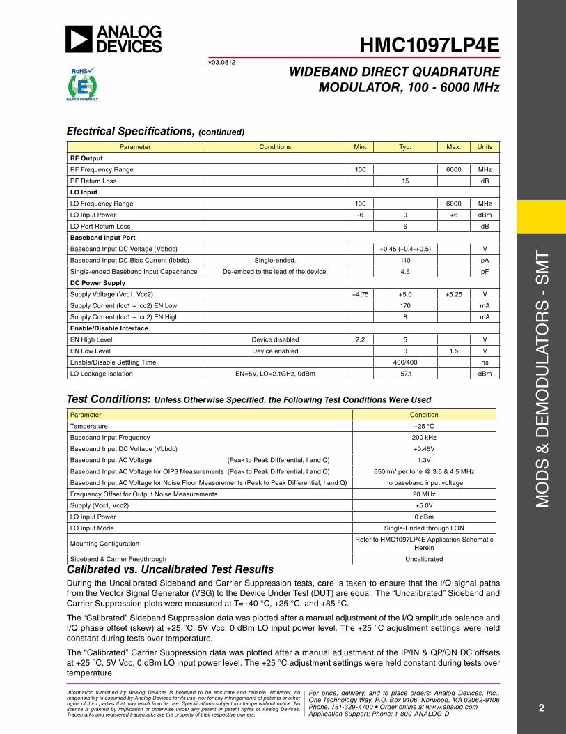
Output Power vs. Frequency Over Temperature
Output IP3, P1dB & Noise Floor @ 20 MHz Offset vs. Frequency Over Temperature
RF and LO Return Loss vs. Frequency
Uncalibrated Carrier Feedthrough [1] vs. Frequency Over Temperature When Disabled
Uncalibrated Carrier Feedthrough [1] vs. Frequency Over Temperature
Calibrated Carrier Feedthrough [1] vs. Frequency Over Temperature
-100
-90
-80
-70
-60
-50
-40
-30
-20
0 1000 2000 3000 4000 5000 6000
+25C+85C-40C
CA
RR
IER
FE
ED
THR
OU
GH
(dB
m)
FREQUENCY (MHz)
-25
-20
-15
-10
-5
0
0 0.5 1 1.5 2 2.5 3 3.5 4 4.5 5 5.5 6
LORF
RE
TU
RN
LO
SS
(dB
)
FREQUENCY (MHz)
-90
-80
-70
-60
-50
-40
-30
-20
-10
0
0 1000 2000 3000 4000 5000 6000
+25C+85C-40C
CA
RR
IER
FE
ED
TH
RO
UG
H (
dBm
)
FREQUENCY (MHz)
-70
-60
-50
-40
-30
-20
-10
0
0 1000 2000 3000 4000 5000 6000
+25C+85C-40CC
AR
RIE
R F
EE
DTH
RO
UG
H (d
Bm
)
FREQUENCY (MHz)
-30
-20
-10
0
10
20
30
40
+25C+85C-40C
-180
-170
-160
-150
-140
-130
-120
-110
0 1000 2000 3000 4000 5000 6000
OU
TP
UT
P1d
B (
dBm
) &
OU
TP
UT
IP3
(dB
m) O
UT
PU
T N
OIS
E F
LOO
R @
20 MH
z (dBm
/Hz)
FREQUENCY (MHz)
NOISE FLOOROUTPUT P1dB
OUTPUT IP3
SET-UP NOISE FLOOR-15
-10
-5
0
5
0 1000 2000 3000 4000 5000 6000
+25C+85C-40C
OU
TPU
T P
OW
ER
(dB
m)
FREQUENCY (MHz)
[1] See note titled “Calibrated vs. Uncalibrated test results” herein.
Information furnished by Analog Devices is believed to be accurate and reliable. However, no responsibility is assumed by Analog Devices for its use, nor for any infringements of patents or other rights of third parties that may result from its use. Specifications subject to change without notice. No license is granted by implication or otherwise under any patent or patent rights of Analog Devices. Trademarks and registered trademarks are the property of their respective owners.
For price, delivery, and to place orders: Analog Devices, Inc., One Technology Way, P.O. Box 9106, Norwood, MA 02062-9106 Phone: 781-329-4700 • Order online at www.analog.com Application Support: Phone: 1-800-ANALOG-D
MO
DS
& D
EM
OD
ULA
TO
RS
- S
MT
4
For price, delivery and to place orders: Hittite Microwave Corporation, 2 Elizabeth Drive, Chelmsford, MA 01824Phone: 978-250-3343 Fax: 978-250-3373 Order On-line at www.hittite.com
Application Support: Phone: 978-250-3343 or [email protected]
v03.0812
WIDEBAND DIRECT QUADRATUREMODULATOR, 100 - 6000 MHz
HMC1097LP4E
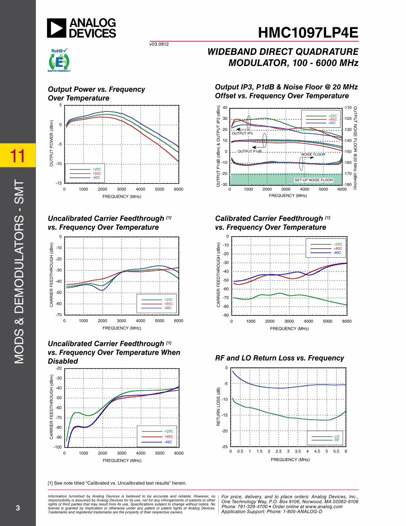
Output Power vs. Frequency Over Supply Voltage
Output IP3, P1dB & Noise Floor @ 20 MHz Offset vs. Frequency Over Supply Voltage
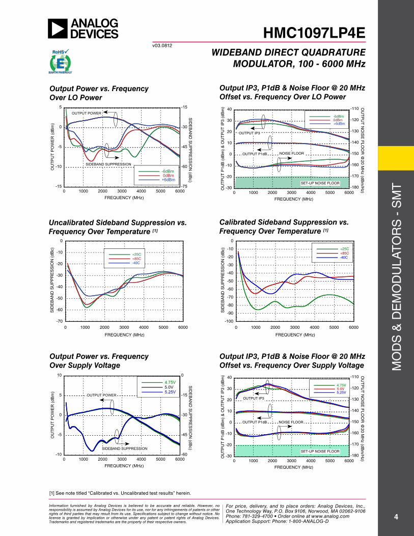
Uncalibrated Sideband Suppression vs. Frequency Over Temperature [1]
Calibrated Sideband Suppression vs. Frequency Over Temperature [1]
Output Power vs. Frequency Over LO Power
Output IP3, P1dB & Noise Floor @ 20 MHz Offset vs. Frequency Over LO Power
[1] See note titled “Calibrated vs. Uncalibrated test results” herein.
-10
-5
0
5
10
4.75V5.0V5.25V
-60
-45
-30
-15
0
0 1000 2000 3000 4000 5000 6000
OU
TPU
T PO
WER
(dBm
)
SIDEBAN
D SU
PPRESSIO
N (dBc)
FREQUENCY (MHz)
SIDEBAND SUPPRESSION
OUTPUT POWER
-30
-20
-10
0
10
20
30
40
4.75V5.0V5.25V
-180
-170
-160
-150
-140
-130
-120
-110
0 1000 2000 3000 4000 5000 6000
OU
TP
UT
P1d
B (
dBm
) &
OU
TP
UT
IP3
(dB
m) O
UT
PU
T N
OIS
E F
LOO
R @
20 MH
z (dBm
/Hz)
FREQUENCY (MHz)
NOISE FLOOROUTPUT P1dB
OUTPUT IP3
SET-UP NOISE FLOOR
-70
-60
-50
-40
-30
-20
-10
0
0 1000 2000 3000 4000 5000 6000
+25C+85C-40C
SID
EB
AN
D S
UP
PR
ES
SIO
N (
dBc)
FREQUENCY (MHz)
-30
-20
-10
0
10
20
30
40
-6dBm 0dBm +6dBm
-180
-170
-160
-150
-140
-130
-120
-110
0 1000 2000 3000 4000 5000 6000
OU
TP
UT
P1d
B (
dBm
) &
OU
TP
UT
IP3
(dB
m) O
UT
PU
T N
OIS
E F
LOO
R @
20 MH
z (dBm
/Hz)
FREQUENCY (MHz)
NOISE FLOOROUTPUT P1dB
OUTPUT IP3
SET-UP NOISE FLOOR-15
-10
-5
0
5
-6dBm 0dBm+6dBm
-75
-60
-45
-30
-15
0 1000 2000 3000 4000 5000 6000
OU
TPU
T P
OW
ER
(dB
m)
SID
EB
AN
D S
UP
PR
ES
SIO
N (dB
c)
FREQUENCY (MHz)
SIDEBAND SUPPRESSION
OUTPUT POWER
-100
-90
-80
-70
-60
-50
-40
-30
-20
-10
0
0 1000 2000 3000 4000 5000 6000
+25C+85C-40C
SID
EB
AN
D S
UP
PR
ES
SIO
N (
dBc)
FREQUENCY (MHz)
Information furnished by Analog Devices is believed to be accurate and reliable. However, no responsibility is assumed by Analog Devices for its use, nor for any infringements of patents or other rights of third parties that may result from its use. Specifications subject to change without notice. No license is granted by implication or otherwise under any patent or patent rights of Analog Devices. Trademarks and registered trademarks are the property of their respective owners.
For price, delivery, and to place orders: Analog Devices, Inc., One Technology Way, P.O. Box 9106, Norwood, MA 02062-9106 Phone: 781-329-4700 • Order online at www.analog.com Application Support: Phone: 1-800-ANALOG-D
MO
DS
& D
EM
OD
ULA
TO
RS
- S
MT
11
5
For price, delivery and to place orders: Hittite Microwave Corporation, 2 Elizabeth Drive, Chelmsford, MA 01824Phone: 978-250-3343 Fax: 978-250-3373 Order On-line at www.hittite.com
Application Support: Phone: 978-250-3343 or [email protected]
v03.0812
WIDEBAND DIRECT QUADRATUREMODULATOR, 100 - 6000 MHz
HMC1097LP4E
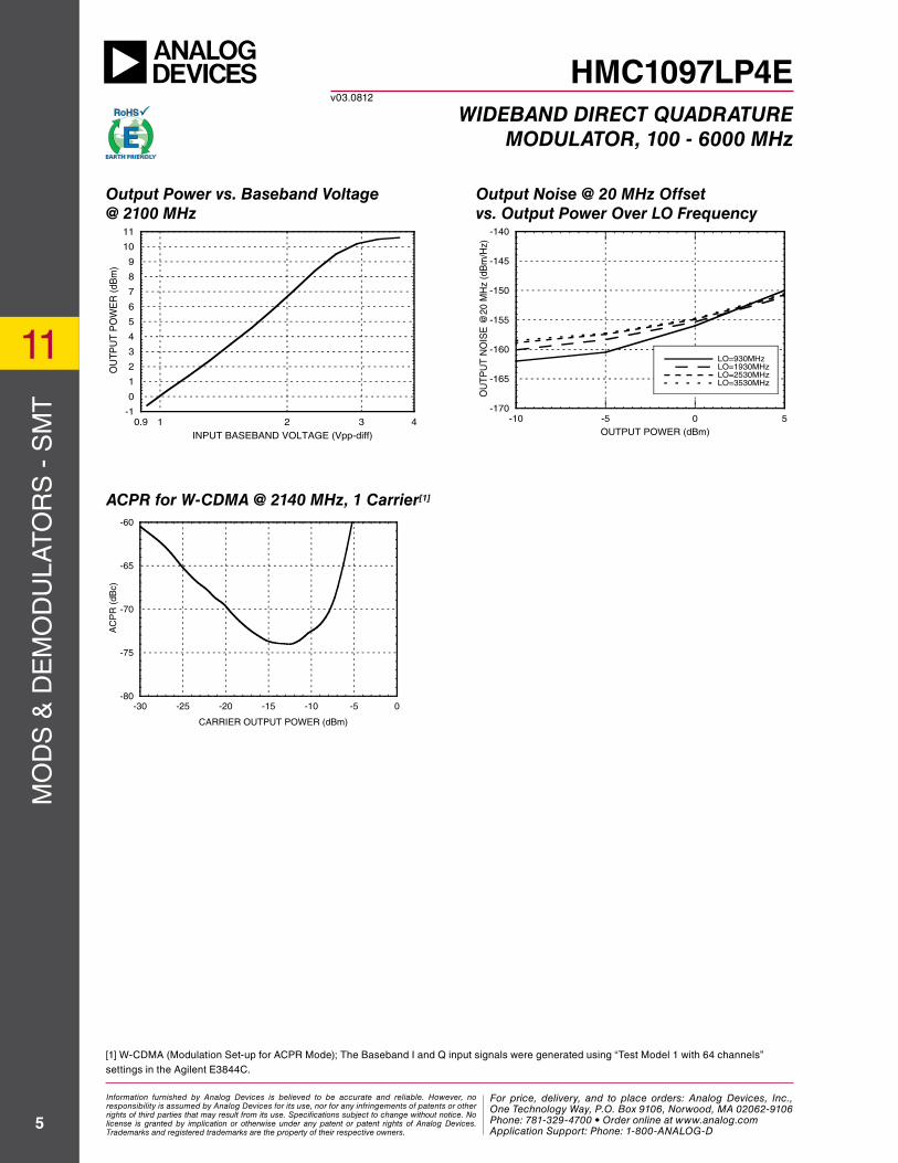
ACPR for W-CDMA @ 2140 MHz, 1 Carrier[1]
[1] W-CDMA (Modulation Set-up for ACPR Mode); The Baseband I and Q input signals were generated using “Test Model 1 with 64 channels” settings in the Agilent E3844C.
-80
-75
-70
-65
-60
-30 -25 -20 -15 -10 -5 0
AC
PR
(dB
c)
CARRIER OUTPUT POWER (dBm)
-1
0
1
2
3
4
5
6
7
8
9
10
11
0.9 1 2 3 4
OU
TP
UT
PO
WE
R (
dBm
)
INPUT BASEBAND VOLTAGE (Vpp-diff)
Output Power vs. Baseband Voltage @ 2100 MHz
-170
-165
-160
-155
-150
-145
-140
-10 -5 0 5
LO=930MHzLO=1930MHzLO=2530MHzLO=3530MHz
OU
TP
UT
NO
ISE
@20
MH
z (d
Bm
/Hz)
OUTPUT POWER (dBm)
Output Noise @ 20 MHz Offsetvs. Output Power Over LO Frequency
Information furnished by Analog Devices is believed to be accurate and reliable. However, no responsibility is assumed by Analog Devices for its use, nor for any infringements of patents or other rights of third parties that may result from its use. Specifications subject to change without notice. No license is granted by implication or otherwise under any patent or patent rights of Analog Devices. Trademarks and registered trademarks are the property of their respective owners.
For price, delivery, and to place orders: Analog Devices, Inc., One Technology Way, P.O. Box 9106, Norwood, MA 02062-9106 Phone: 781-329-4700 • Order online at www.analog.com Application Support: Phone: 1-800-ANALOG-D
MO
DS
& D
EM
OD
ULA
TO
RS
- S
MT
6
For price, delivery and to place orders: Hittite Microwave Corporation, 2 Elizabeth Drive, Chelmsford, MA 01824Phone: 978-250-3343 Fax: 978-250-3373 Order On-line at www.hittite.com
Application Support: Phone: 978-250-3343 or [email protected]
v03.0812
WIDEBAND DIRECT QUADRATUREMODULATOR, 100 - 6000 MHz
HMC1097LP4E
Absolute Maximum RatingsVcc1, Vcc2, EN 0V to +5.6V
LO Input Power +18 dBm
Baseband Input Voltage (AC + DC)(Reference to GND)
-0.3V to + 1.3V
Junction Temperature 125°C
Continuous Pdiss (T = 85°C)(Derate 30 mW/°C above 85°C)
2.05 Watts
Thermal Resistance (Rth)(junction to ground paddle)
9°C/W
Storage Temperature -65 to +150 °C
Operating Temperature -40 to +85 °C
ESD Sensitivity (HBM) Class 1B
Outline Drawing
ELECTROSTATIC SENSITIVE DEVICEOBSERVE HANDLING PRECAUTIONS
NOTES:
1. PACKAGE BODY MATERIAL: LOW STRESS INJECTION MOLDED PLASTIC SILICA AND SILICON IMPREGNATED.
2. LEAD AND GROUND PADDLE MATERIAL: COPPER ALLOY.
3. LEAD AND GROUND PADDLE PLATING: 100% MATTE TIN.
4. DIMENSIONS ARE IN INCHES [MILLIMETERS].
5. LEAD SPACING TOLERANCE IS NON-CUMULATIVE.
6. CHARACTERS TO BE HELVETICA MEDIUM, .025 HIGH, WHITE INK, OR LASER MARK LOCATED APPROX. AS SHOWN.
7. PAD BURR LENGTH SHALL BE 0.15mm MAX. PAD BURR HEIGHT SHALL BE 0.25mm MAX.
8. PACKAGE WARP SHALL NOT EXCEED 0.05mm
9. ALL GROUND LEADS AND GROUND PADDLE MUST BE SOLDERED TO PCB RF GROUND.
10. REFER TO HITTITE APPLICATION NOTE FOR SUGGESTED PCB LAND PATTERN.
Part Number Package Body Material Lead Finish MSL Rating Package Marking [2]
HMC1097LP4E RoHS-compliant Low Stress Injection Molded Plastic 100% matte Sn MSL1 [1] H1097XXXX
[1] Max peak reflow temperature of 260 °C[2] 4-Digit lot number XXXX
Package Information
Information furnished by Analog Devices is believed to be accurate and reliable. However, no responsibility is assumed by Analog Devices for its use, nor for any infringements of patents or other rights of third parties that may result from its use. Specifications subject to change without notice. No license is granted by implication or otherwise under any patent or patent rights of Analog Devices. Trademarks and registered trademarks are the property of their respective owners.
For price, delivery, and to place orders: Analog Devices, Inc., One Technology Way, P.O. Box 9106, Norwood, MA 02062-9106 Phone: 781-329-4700 • Order online at www.analog.com Application Support: Phone: 1-800-ANALOG-D
MO
DS
& D
EM
OD
ULA
TO
RS
- S
MT
11
7
For price, delivery and to place orders: Hittite Microwave Corporation, 2 Elizabeth Drive, Chelmsford, MA 01824Phone: 978-250-3343 Fax: 978-250-3373 Order On-line at www.hittite.com
Application Support: Phone: 978-250-3343 or [email protected]
v03.0812
WIDEBAND DIRECT QUADRATUREMODULATOR, 100 - 6000 MHz
HMC1097LP4E
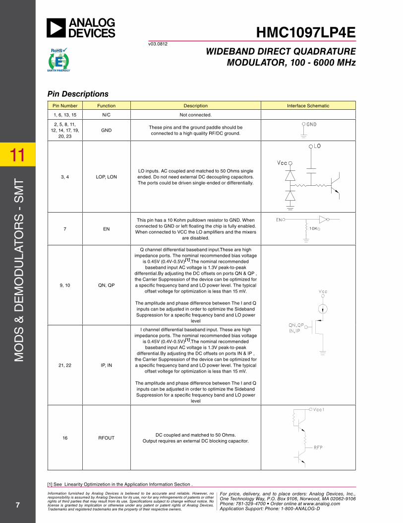
Pin Number Function Description Interface Schematic
1, 6, 13, 15 N/C Not connected.
2, 5, 8, 11, 12, 14, 17, 19,
20, 23GND
These pins and the ground paddle should be connected to a high quality RF/DC ground.
3, 4 LOP, LONLO inputs. AC coupled and matched to 50 Ohms single ended. Do not need external DC decoupling capacitors. The ports could be driven single-ended or differentially.
7 EN
This pin has a 10 Kohm pulldown resistor to GND. When connected to GND or left floating the chip is fully enabled.When connected to VCC the LO amplifiers and the mixers
are disabled.
9, 10 QN, QP
Q channel differential baseband input.These are high impedance ports. The nominal recommended bias voltage
is 0.45V (0.4V-0.5V)[1].The nominal recommended baseband input AC voltage is 1.3V peak-to-peak
differential.By adjusting the DC offsets on ports QN & QP , the Carrier Suppression of the device can be optimized for a specific frequency band and LO power level. The typical
offset voltege for optimization is less than 15 mV.
The amplitude and phase difference between The I and Q inputs can be adjusted in order to optimize the Sideband Suppression for a specific frequency band and LO power
level
21, 22 IP, IN
I channel differential baseband input. These are high impedance ports. The nominal recommended bias voltage
is 0.45V (0.4V-0.5V)[1].The nominal recommended baseband input AC voltage is 1.3V peak-to-peak
differential.By adjusting the DC offsets on ports IN & IP , the Carrier Suppression of the device can be optimized for a specific frequency band and LO power level. The typical
offset voltege for optimization is less than 15 mV.
The amplitude and phase difference between The I and Q inputs can be adjusted in order to optimize the Sideband Suppression for a specific frequency band and LO power
level
16 RFOUTDC coupled and matched to 50 Ohms.
Output requires an external DC blocking capacitor.
Pin Descriptions
[1] See Linearity Optimizetion in the Application Information Section .
Information furnished by Analog Devices is believed to be accurate and reliable. However, no responsibility is assumed by Analog Devices for its use, nor for any infringements of patents or other rights of third parties that may result from its use. Specifications subject to change without notice. No license is granted by implication or otherwise under any patent or patent rights of Analog Devices. Trademarks and registered trademarks are the property of their respective owners.
For price, delivery, and to place orders: Analog Devices, Inc., One Technology Way, P.O. Box 9106, Norwood, MA 02062-9106 Phone: 781-329-4700 • Order online at www.analog.com Application Support: Phone: 1-800-ANALOG-D
MO
DS
& D
EM
OD
ULA
TO
RS
- S
MT
8
For price, delivery and to place orders: Hittite Microwave Corporation, 2 Elizabeth Drive, Chelmsford, MA 01824Phone: 978-250-3343 Fax: 978-250-3373 Order On-line at www.hittite.com
Application Support: Phone: 978-250-3343 or [email protected]
v03.0812
WIDEBAND DIRECT QUADRATUREMODULATOR, 100 - 6000 MHz
HMC1097LP4E
Pin Number Function Description Interface Schematic
18 Vcc1 Supply voltage for the output stages 30 mA @ +5V.
24 Vcc2 Supply voltage for the LO and mixer stage 140 mA @ +5V.
Pin Descriptions (continued)
Application & Evaluation PCB Schematic
Information furnished by Analog Devices is believed to be accurate and reliable. However, no responsibility is assumed by Analog Devices for its use, nor for any infringements of patents or other rights of third parties that may result from its use. Specifications subject to change without notice. No license is granted by implication or otherwise under any patent or patent rights of Analog Devices. Trademarks and registered trademarks are the property of their respective owners.
For price, delivery, and to place orders: Analog Devices, Inc., One Technology Way, P.O. Box 9106, Norwood, MA 02062-9106 Phone: 781-329-4700 • Order online at www.analog.com Application Support: Phone: 1-800-ANALOG-D
MO
DS
& D
EM
OD
ULA
TO
RS
- S
MT
11
9
For price, delivery and to place orders: Hittite Microwave Corporation, 2 Elizabeth Drive, Chelmsford, MA 01824Phone: 978-250-3343 Fax: 978-250-3373 Order On-line at www.hittite.com
Application Support: Phone: 978-250-3343 or [email protected]
v03.0812
WIDEBAND DIRECT QUADRATUREMODULATOR, 100 - 6000 MHz
HMC1097LP4E
Item Description
J1 - J7 PC Mount SMA Connector
J8-J10 DC Molex Connector
C1 - C3 100 pF Chip Capacitor, 0402 Pkg.
C8, C9 1000 pF Chip Capacitor, 0402 Pkg.
C10, C11 4.7 uF, Case A, Tantalum
R2 0 Ohm Resistor, 0402 Pkg.
R3 49.9 Ohm Resistor, 0402 Pkg.
U1 HMC1097LP4E Modulator
PCB [2] 600-00313-00-1 Evaluation PCB
[1] Reference this number when ordering complete evaluation PCB
[2] Circuit Board Material: Rogers 4350
Evaluation PCB
The circuit board used in the application should use RF circuit design techniques. Signal lines should have 50 ohm impedance while the package ground leads and exposed paddle should be connected directly to the ground plane similar to that shown. A sufficient number of via holes should be used to connect the top and bottom ground planes. The evaluation circuit board shown is available from Hittite upon request.
List of Materials for Evaluation PCB EVAL01-HMC1097LP4E[1]
Information furnished by Analog Devices is believed to be accurate and reliable. However, no responsibility is assumed by Analog Devices for its use, nor for any infringements of patents or other rights of third parties that may result from its use. Specifications subject to change without notice. No license is granted by implication or otherwise under any patent or patent rights of Analog Devices. Trademarks and registered trademarks are the property of their respective owners.
For price, delivery, and to place orders: Analog Devices, Inc., One Technology Way, P.O. Box 9106, Norwood, MA 02062-9106 Phone: 781-329-4700 • Order online at www.analog.com Application Support: Phone: 1-800-ANALOG-D
MO
DS
& D
EM
OD
ULA
TO
RS
- S
MT
10
For price, delivery and to place orders: Hittite Microwave Corporation, 2 Elizabeth Drive, Chelmsford, MA 01824Phone: 978-250-3343 Fax: 978-250-3373 Order On-line at www.hittite.com
Application Support: Phone: 978-250-3343 or [email protected]
v03.0812
WIDEBAND DIRECT QUADRATUREMODULATOR, 100 - 6000 MHz
HMC1097LP4E
Characterization Set-up
Information furnished by Analog Devices is believed to be accurate and reliable. However, no responsibility is assumed by Analog Devices for its use, nor for any infringements of patents or other rights of third parties that may result from its use. Specifications subject to change without notice. No license is granted by implication or otherwise under any patent or patent rights of Analog Devices. Trademarks and registered trademarks are the property of their respective owners.
For price, delivery, and to place orders: Analog Devices, Inc., One Technology Way, P.O. Box 9106, Norwood, MA 02062-9106 Phone: 781-329-4700 • Order online at www.analog.com Application Support: Phone: 1-800-ANALOG-D
MO
DS
& D
EM
OD
ULA
TO
RS
- S
MT
11
11
For price, delivery and to place orders: Hittite Microwave Corporation, 2 Elizabeth Drive, Chelmsford, MA 01824Phone: 978-250-3343 Fax: 978-250-3373 Order On-line at www.hittite.com
Application Support: Phone: 978-250-3343 or [email protected]
v03.0812
WIDEBAND DIRECT QUADRATUREMODULATOR, 100 - 6000 MHz
HMC1097LP4E
Application InformationPrinciple of Operation
Figure 1: The HMC1097LP4E Simplified Block Diagram
The HMC1097LP4E is a low-noise, high-linearity, broadband Direct Quadrature Modulator designed for directly converting complex modulated baseband signals from zero IF or low IF to RF transmission levels from 100 MHz to 6 GHz. The HMC1097LP4E’s excellent noise and linearity performance makes it suitable for a wide range of transmission standards, including single and multicarrier CDMA, UMTS, CDMA2000, GSM/EDGE, W-CDMA, TD-SCDMA, and WiMAX/LTE applications.
As shown in the simplified block diagram (Figure 1) the HMC1097LP4E offers an easy-to-use, complete direct conversion solution in a highly compact 4 x 4 mm plastic package thereby reducing cost, area, and power consumption.
The HMC1097LP4E modulator consists of the following functional blocks:
1. LO Interface: High Accuracy LO quadrature phase splitter and LO limiting amplifiers
2. I/Q modulator: I and Q input differential voltage-to-current converters, I and Q upconverting mixers and the differential-to-single-ended converter
3. Bias and Enable/Disable Circuits
LO InterfaceThe LO interface consists of a LO quadrature phase splitter that generates two carrier signals in quadrature followed by LO limiting amplifiers which are used to drive the I and Q mixers with saturated signal levels. Therefore, the LO path is immune to large variations in the LO input signal level and the modulator performance does not vary much
Information furnished by Analog Devices is believed to be accurate and reliable. However, no responsibility is assumed by Analog Devices for its use, nor for any infringements of patents or other rights of third parties that may result from its use. Specifications subject to change without notice. No license is granted by implication or otherwise under any patent or patent rights of Analog Devices. Trademarks and registered trademarks are the property of their respective owners.
For price, delivery, and to place orders: Analog Devices, Inc., One Technology Way, P.O. Box 9106, Norwood, MA 02062-9106 Phone: 781-329-4700 • Order online at www.analog.com Application Support: Phone: 1-800-ANALOG-D
MO
DS
& D
EM
OD
ULA
TO
RS
- S
MT
12
For price, delivery and to place orders: Hittite Microwave Corporation, 2 Elizabeth Drive, Chelmsford, MA 01824Phone: 978-250-3343 Fax: 978-250-3373 Order On-line at www.hittite.com
Application Support: Phone: 978-250-3343 or [email protected]
v03.0812
WIDEBAND DIRECT QUADRATUREMODULATOR, 100 - 6000 MHz
HMC1097LP4E
with LO input power.
The LO input impedance is set by the LO quadrature phase splitter. The LO port can be driven differentially with 100 Ω differential input impedance or single ended through LON input with 50Ω input impedance while the unused LOP input should be terminated to GND through 50Ω. The LO port requires -6 to +6 dBm input power in either differential or single-ended mode and does not require DC blocking capacitors.
I/Q ModulatorThe differential baseband inputs (QP, QN, IP, and IN) present a high impedance. The DC common-mode voltage at the baseband inputs sets the currents in the I and Q double-balanced mixers. The nominal baseband input DC common-mode voltage used in the characterization of the HMC1097LP4E is 0.45V, which should be externally applied. The baseband input DC common-mode voltage can be varied between 0.4V and 0.5V to optimize overall modulator performance. It is not recommended to leave the baseband inputs floating which generates excessive current flow that may cause damage to the IC. The baseband inputs should be pulled down to GND in shutdown mode. The nominal baseband input AC Voltage used in the characterization of the HMC1097LP4E is 1.3Vpp differential. The baseband input AC voltage can be varied to optimize overall modulator performance.
It is recommended to drive the baseband inputs differentially to reduce even-order distortion products and also use reconstruction filters at the baseband inputs to avoid aliasing
After upconversion, the outputs of the I and Q mixers are summed together differentially and converted to single- ended RF output. The single-ended RF output port is internally matched to 50 Ohms and does not require any external matching components. Only a standard DC-blocking capacitor is required at this interface.
Bias and Enable/Disable CircuitsA bandgap reference circuit generates the reference currents used by the different sections. The part requires a single supply voltage of +5V to operate.
The EN pin can be used to disable the bandgap reference circuit. Disabling the bias circuit will also disable the reference currents to the LO limiting amplifiers,I and Q mixers and the output stage. If the EN pin is connected to ground or left floating, the part operates normally. If the EN pin is connected to the +5V VCC, the LO limiting amplifiers, I and Q mixers and the output stage are disabled and the LO leakage is also reduced. The LO signal itself is suppressed approximately by 57.1 dB at 2.1GHz when the EN pin is connected to the +5V VCC. The enable and disable settling times are approximately 400 ns.
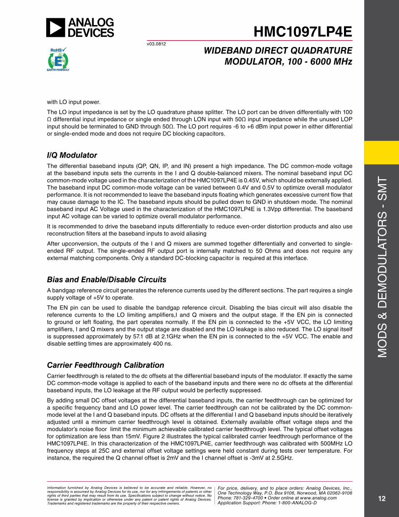
Carrier Feedthrough CalibrationCarrier feedthrough is related to the dc offsets at the differential baseband inputs of the modulator. If exactly the same DC common-mode voltage is applied to each of the baseband inputs and there were no dc offsets at the differential baseband inputs, the LO leakage at the RF output would be perfectly suppressed.
By adding small DC offset voltages at the differential baseband inputs, the carrier feedthrough can be optimized for a specific frequency band and LO power level. The carrier feedthrough can not be calibrated by the DC common-mode level at the I and Q baseband inputs. DC offsets at the differential I and Q baseband inputs should be iteratively adjusted until a minimum carrier feedthrough level is obtained. Externally available offset voltage steps and the modulator’s noise floor limit the minimum achievable calibrated carrier feedthrough level. The typical offset voltages for optimization are less than 15mV. Figure 2 illustrates the typical calibrated carrier feedthrough performance of the HMC1097LP4E. In this characterization of the HMC1097LP4E, carrier feedthrough was calibrated with 500MHz LO frequency steps at 25C and external offset voltage settings were held constant during tests over temperature. For instance, the required the Q channel offset is 2mV and the I channel offset is -3mV at 2.5GHz.
Information furnished by Analog Devices is believed to be accurate and reliable. However, no responsibility is assumed by Analog Devices for its use, nor for any infringements of patents or other rights of third parties that may result from its use. Specifications subject to change without notice. No license is granted by implication or otherwise under any patent or patent rights of Analog Devices. Trademarks and registered trademarks are the property of their respective owners.
For price, delivery, and to place orders: Analog Devices, Inc., One Technology Way, P.O. Box 9106, Norwood, MA 02062-9106 Phone: 781-329-4700 • Order online at www.analog.com Application Support: Phone: 1-800-ANALOG-D
MO
DS
& D
EM
OD
ULA
TO
RS
- S
MT
11
13
For price, delivery and to place orders: Hittite Microwave Corporation, 2 Elizabeth Drive, Chelmsford, MA 01824Phone: 978-250-3343 Fax: 978-250-3373 Order On-line at www.hittite.com
Application Support: Phone: 978-250-3343 or [email protected]
v03.0812
WIDEBAND DIRECT QUADRATUREMODULATOR, 100 - 6000 MHz
HMC1097LP4E
-90
-80
-70
-60
-50
-40
-30
-20
-10
0
0 1000 2000 3000 4000 5000 6000
+25C+85C-40C
CA
RR
IER
FE
ED
TH
RO
UG
H (
dBm
)
FREQUENCY (MHz)
Figure 2: The HMC1097LP4E Calibrated Carrier Feedthrough
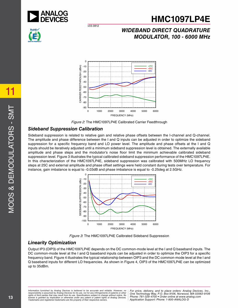
Sideband Suppression CalibrationSideband suppression is related to relative gain and relative phase offsets between the I-channel and Q-channel. The amplitude and phase difference between the I and Q inputs can be adjusted in order to optimize the sideband suppression for a specific frequency band and LO power level. The amplitude and phase offsets at the I and Q inputs should be iteratively adjusted until a minimum sideband suppression level is obtained. The externally available amplitude and phase steps and the modulator’s noise floor limit the minimum achievable calibrated sideband suppression level. Figure 3 illustrates the typical calibrated sideband suppression performance of the HMC1097LP4E. In this characterization of the HMC1097LP4E, sideband suppression was calibrated with 500MHz LO frequency steps at 25C and external amplitude and phase offset settings were held constant during tests over temperature. For instance, gain imbalance is equal to -0.03dB and phase imbalance is equal to -0.25deg at 2.5GHz.
-100
-90
-80
-70
-60
-50
-40
-30
-20
-10
0
0 1000 2000 3000 4000 5000 6000
+25C+85C-40C
SID
EB
AN
D S
UP
PR
ES
SIO
N (
dBc)
FREQUENCY (MHz)
Figure 3: The HMC1097LP4E Calibrated Sideband Suppression
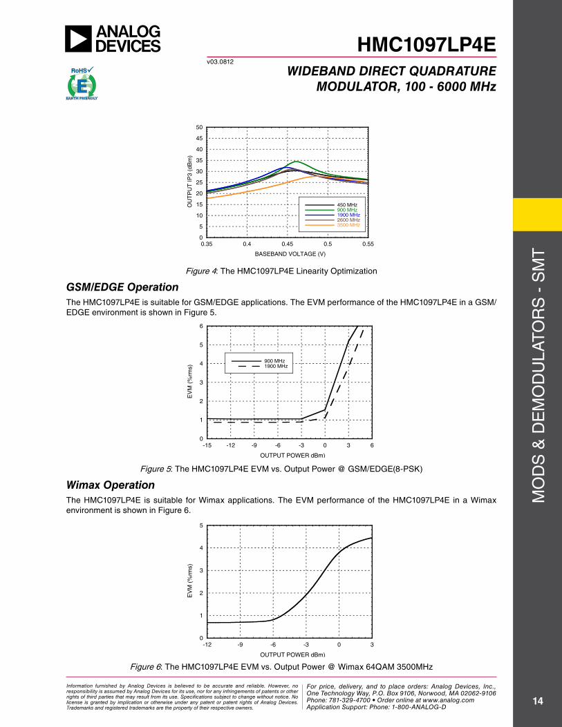
Linearity OptimizationOutput IP3 (OIP3) of the HMC1097LP4E depends on the DC common-mode level at the I and Q baseband inputs. The DC common-mode level at the I and Q baseband inputs can be adjusted in order to optimize the OIP3 for a specific frequency band. Figure 4 illustrates the typical relationship between OIP3 and the DC common-mode level at the I and Q baseband inputs for different LO frequencies. As shown in Figure 4, OIP3 of the HMC1097LP4E can be optimized up to 35dBm.
Information furnished by Analog Devices is believed to be accurate and reliable. However, no responsibility is assumed by Analog Devices for its use, nor for any infringements of patents or other rights of third parties that may result from its use. Specifications subject to change without notice. No license is granted by implication or otherwise under any patent or patent rights of Analog Devices. Trademarks and registered trademarks are the property of their respective owners.
For price, delivery, and to place orders: Analog Devices, Inc., One Technology Way, P.O. Box 9106, Norwood, MA 02062-9106 Phone: 781-329-4700 • Order online at www.analog.com Application Support: Phone: 1-800-ANALOG-D
MO
DS
& D
EM
OD
ULA
TO
RS
- S
MT
14
For price, delivery and to place orders: Hittite Microwave Corporation, 2 Elizabeth Drive, Chelmsford, MA 01824Phone: 978-250-3343 Fax: 978-250-3373 Order On-line at www.hittite.com
Application Support: Phone: 978-250-3343 or [email protected]
v03.0812
WIDEBAND DIRECT QUADRATUREMODULATOR, 100 - 6000 MHz
HMC1097LP4E
0
5
10
15
20
25
30
35
40
45
50
0.35 0.4 0.45 0.5 0.55
450 MHz900 MHz1900 MHz2600 MHz3500 MHz
OU
TP
UT
IP3
(dB
m)
BASEBAND VOLTAGE (V)
Figure 4: The HMC1097LP4E Linearity Optimization
GSM/EDGE OperationThe HMC1097LP4E is suitable for GSM/EDGE applications. The EVM performance of the HMC1097LP4E in a GSM/EDGE environment is shown in Figure 5.
0
1
2
3
4
5
6
-15 -12 -9 -6 -3 0 3 6
900 MHz1900 MHz
EV
M (
%rm
s)
OUTPUT POWER dBm)
Figure 5: The HMC1097LP4E EVM vs. Output Power @ GSM/EDGE(8-PSK)
Wimax OperationThe HMC1097LP4E is suitable for Wimax applications. The EVM performance of the HMC1097LP4E in a Wimax environment is shown in Figure 6.
0
1
2
3
4
5
-12 -9 -6 -3 0 3
EV
M (
%rm
s)
OUTPUT POWER dBm)
Figure 6: The HMC1097LP4E EVM vs. Output Power @ Wimax 64QAM 3500MHz
Information furnished by Analog Devices is believed to be accurate and reliable. However, no responsibility is assumed by Analog Devices for its use, nor for any infringements of patents or other rights of third parties that may result from its use. Specifications subject to change without notice. No license is granted by implication or otherwise under any patent or patent rights of Analog Devices. Trademarks and registered trademarks are the property of their respective owners.
For price, delivery, and to place orders: Analog Devices, Inc., One Technology Way, P.O. Box 9106, Norwood, MA 02062-9106 Phone: 781-329-4700 • Order online at www.analog.com Application Support: Phone: 1-800-ANALOG-D
MO
DS
& D
EM
OD
ULA
TO
RS
- S
MT
11
15
For price, delivery and to place orders: Hittite Microwave Corporation, 2 Elizabeth Drive, Chelmsford, MA 01824Phone: 978-250-3343 Fax: 978-250-3373 Order On-line at www.hittite.com
Application Support: Phone: 978-250-3343 or [email protected]
v03.0812
WIDEBAND DIRECT QUADRATUREMODULATOR, 100 - 6000 MHz
HMC1097LP4E
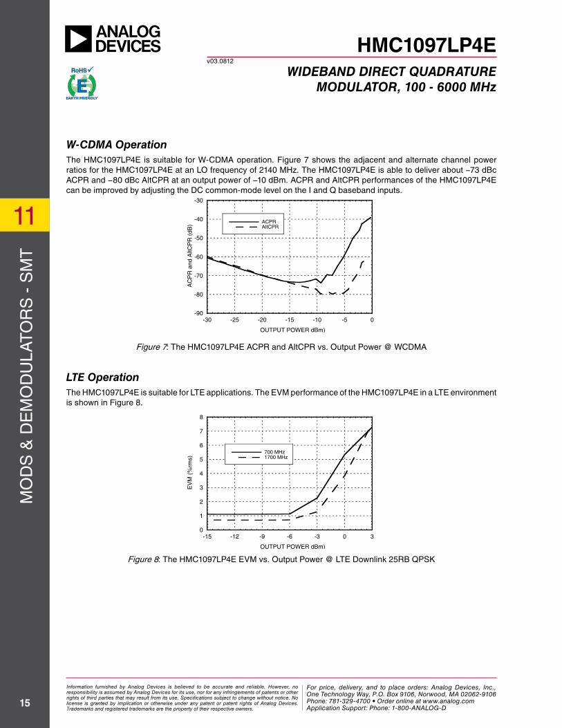
W-CDMA OperationThe HMC1097LP4E is suitable for W-CDMA operation. Figure 7 shows the adjacent and alternate channel power ratios for the HMC1097LP4E at an LO frequency of 2140 MHz. The HMC1097LP4E is able to deliver about −73 dBc ACPR and −80 dBc AltCPR at an output power of −10 dBm. ACPR and AltCPR performances of the HMC1097LP4E can be improved by adjusting the DC common-mode level on the I and Q baseband inputs.
-90
-80
-70
-60
-50
-40
-30
-30 -25 -20 -15 -10 -5 0
ACPRAltCPR
AC
PR
and
AltC
PR
(dB
)
OUTPUT POWER dBm)
Figure 7: The HMC1097LP4E ACPR and AltCPR vs. Output Power @ WCDMA
LTE OperationThe HMC1097LP4E is suitable for LTE applications. The EVM performance of the HMC1097LP4E in a LTE environment is shown in Figure 8.
0
1
2
3
4
5
6
7
8
-15 -12 -9 -6 -3 0 3
700 MHz1700 MHz
EV
M (
%rm
s)
OUTPUT POWER dBm)
Figure 8: The HMC1097LP4E EVM vs. Output Power @ LTE Downlink 25RB QPSK
Information furnished by Analog Devices is believed to be accurate and reliable. However, no responsibility is assumed by Analog Devices for its use, nor for any infringements of patents or other rights of third parties that may result from its use. Specifications subject to change without notice. No license is granted by implication or otherwise under any patent or patent rights of Analog Devices. Trademarks and registered trademarks are the property of their respective owners.
For price, delivery, and to place orders: Analog Devices, Inc., One Technology Way, P.O. Box 9106, Norwood, MA 02062-9106 Phone: 781-329-4700 • Order online at www.analog.com Application Support: Phone: 1-800-ANALOG-D