Embed Size (px)
Citation preview
For price, delivery, and to place orders, please contact Hittite Microwave Corporation:20 Alpha Road, Chelmsford, MA 01824 Phone: 978-250-3343 Fax: 978-250-3373
Order On-line at www.hittite.com
HIG
H S
PE
ED
LO
GIC
- S
MT
7
7 - 1
The HMC841LC4B is a D-type Flip Flop designed to support data transmission rates of up to 43 Gbps, and clock frequencies as high as 43 GHz. During normal operation, data is transferred to the outputs on the positive edge of the clock. Reversing the clock inputs allows for negative-edge triggered applications. The HMC841LC4B also features an output level control pin, VAC, which allows for loss compensation or for signal level optimization.
All input signals to the HMC841LC4B are terminated with 50 Ohms to ground on-chip, and maybe either AC or DC coupled. The differential outputs of the HMC841LC4B may be either AC or DC coupled. Outputs can be connected directly to a 50 Ohms-to-ground terminated system, while DC blocking capacitors should be used if the terminating system is 50 Ohms to a non-ground DC voltage. The HMC841LC4B operates from a single -3.3V DC supply and is available in a ceramic RoHS compliant 4x4 mm SMT package.
General Description
HMC841LC4B
Features
Functional Diagram
Supports Data Rates up to 43 Gbps
Low Power Consumption: 630 mW
Fast Rise and Fall Times: 12/12 ps
Single Ended or Differential Operation
Adjustable Differential Output Voltage Swing: 200 - 850 mVp-p
24 Lead 4x4mm SMT Package: 16mm2
Typical Applications
The HMC841LC4B is ideal for:
• OC-768 and SDH STM-256 Equipment
• RF ATE Applications
• Serial Data Transmission up to 43 Gbps
• Digital Logic Systems up to 43 Gbps
• Broadband Test & Measurement
Electrical Specifications, TA = +25°C, Vee = -3.3V
Parameter Conditions Min. Typ. Max Units
Power Supply Voltage ±5 % Tolerance -3.47 -3.3 -3.13 V
Power Supply Current VAC = -0.3V 160 190 220 mA
Output Amplitude Control Voltage VAC -1.6 -0.3 -0.1 V
Maximum Data Rate 43 Gbps
Maximum Clock Rate 43 GHz
Input Amplitude (Data)Single-ended, peak-to-peak 200 800
mVp-pDifferential, peak-to-peak 200 1000
Input Amplitude (Clock)Single-ended, peak-to-peak 400 800
mVp-pDifferential, peak-to-peak 250 1000
Input High Voltage (Data & Clock) -0.5 0.5 V
Input Low Voltage (Data & Clock) -1 0 V
43 Gbps, D-TYPE FLIP-FLOPw/ PROGRAMMABLE OUTPUT VOLTAGE
v02.0910
www.BDTIC.com/Hittite/
For price, delivery, and to place orders, please contact Hittite Microwave Corporation:20 Alpha Road, Chelmsford, MA 01824 Phone: 978-250-3343 Fax: 978-250-3373
Order On-line at www.hittite.com
HIG
H S
PE
ED
LO
GIC
- S
MT
7
7 - 2
Electrical Specifications, (continued)
HMC841LC4Bv02.0910
43 Gbps, D-TYPE FLIP-FLOPw/ PROGRAMMABLE OUTPUT VOLTAGE
Parameter Conditions Min. Typ. Max Units
Output Amplitude Differential, peak-to-peak @ 40 Gbps 200 850 mVp-p
Output High Voltage VAC = -0.3 -50 mV
Output Low Voltage VAC = -0.3 -550 mV
Input Return LossData input up to 25 GHz 10 dB
Clock input up to 40 GHz 6 dB
Output Return Loss Data output up to 25 GHz 10 dB
Deterministic Jitter, Jd [1] 2 ps, pp
Additive Random Jitter Jr [2] 0.2 ps rms
Rise Time, tr [1] 12 ps
Fall Time, tf [1] 12 ps
Propagation Delay, td Clock to output delay 10 ps
Clock Phase Margin @ 40 Gbps 270 deg
[1] Clock Input: 40 GHz clock signal, 200 mVp-p single-ended, Data Input: 40 Gbps PRBS 223-1 pattern, 200 mVp-p single-ended[2] Random jitter is measured with 40 Gbps 10101… pattern
[1] VAC = -0.3V [2] Input data rate: 40 Gbps PRBS 223-1
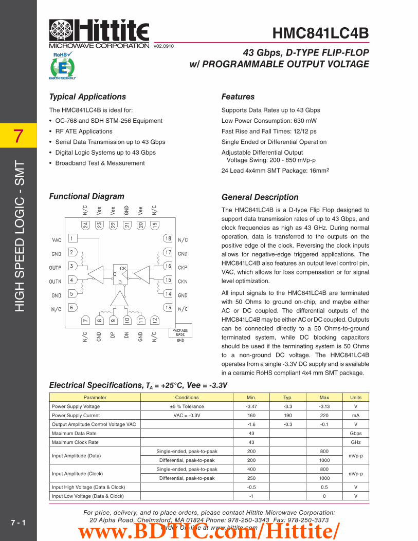
DC Current vs. Supply Voltage [1] [2]
Differential Output Swing vs. Supply Voltage [1] [2]
DC Current vs. VAC [2] Differential Output Swing vs. VAC [2]
100
125
150
175
200
225
250
-3.47 -3.41 -3.36 -3.3 -3.24 -3.19 -3.13
+25C+70C -40C
SUPPLY VOLTAGE Vee (V)
DC
CU
RR
EN
T (
mA
)
100
125
150
175
200
225
250
-1.6 -1.3 -1 -0.7 -0.4 -0.1
+25C+70C -40C
CONTROL VOLTAGE VAC (V)
DC
CU
RR
EN
T (
mA
)
600
700
800
900
1000
-3.47 -3.41 -3.36 -3.3 -3.24 -3.19 -3.13
+25C+70C -40C
SUPPLY VOLTAGE Vee (V)
DIF
FE
RE
NT
IAL
VO
LTA
GE
(m
Vp-
p)
0
200
400
600
800
1000
-1.6 -1.3 -1 -0.7 -0.4 -0.1
+25C+70C -40C
CONTROL VOLTAGE VAC (V)
DIF
FE
RE
NT
IAL
VO
LTA
GE
(m
Vp-
p)
www.BDTIC.com/Hittite/
For price, delivery, and to place orders, please contact Hittite Microwave Corporation:20 Alpha Road, Chelmsford, MA 01824 Phone: 978-250-3343 Fax: 978-250-3373
Order On-line at www.hittite.com
HIG
H S
PE
ED
LO
GIC
- S
MT
7
7 - 3
HMC841LC4Bv02.0910
43 Gbps, D-TYPE FLIP-FLOPw/ PROGRAMMABLE OUTPUT VOLTAGE
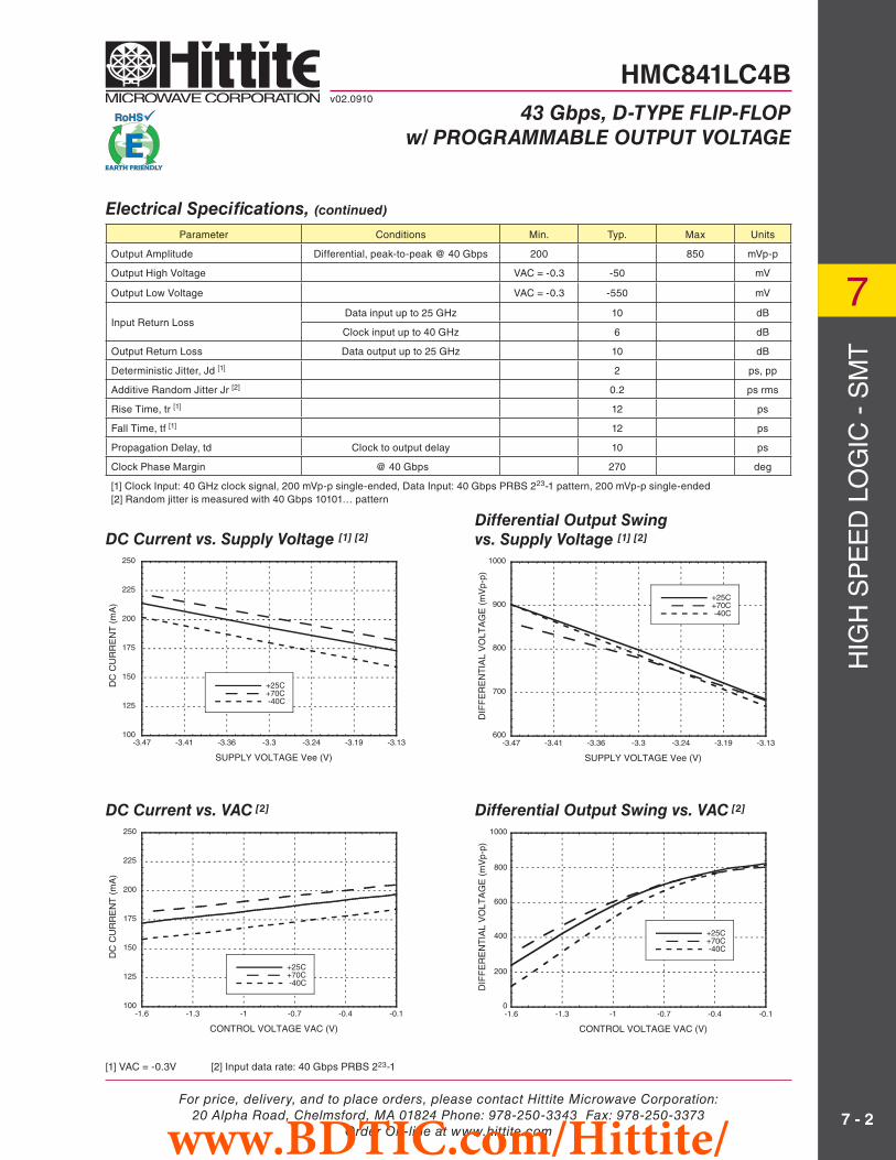
Rise / Fall Time vs. VAC [1][2][3]
Input Return Loss vs. Frequency [1][5]
Peak-to-Peak Jitter vs. Supply Voltage [1][2][3][4]
Output Return Loss vs. Frequency [1][5]
Fall Time vs. Supply Voltage [1][2][3]Rise Time vs. Supply Voltage [1][2][3]
0
3
6
9
12
15
18
-3.47 -3.41 -3.36 -3.3 -3.24 -3.19 -3.13
+25C+70C -40C
SUPPLY VOLTAGE Vee (V)
RIS
E T
IME
(ps
)
0
3
6
9
12
15
18
-1.6 -1.3 -1 -0.7 -0.4 -0.1
Rise TimeFall Time
CONTROL VOLTAGE VAC (V)
RIS
E/F
ALL
TIM
E (
ps)
-30
-25
-20
-15
-10
-5
0
0 5 10 15 20 25 30 35 40 45 50
DataClock
FREQUENCY (GHz)
RE
SP
ON
SE
(dB
)
0
3
6
9
12
15
18
-3.47 -3.41 -3.36 -3.3 -3.24 -3.19 -3.13
+25C+70C -40C
SUPPLY VOLTAGE Vee (V)
FA
LL T
IME
(ps
)
0
2
4
6
8
10
12
-3.47 -3.41 -3.36 -3.3 -3.24 -3.19 -3.13
+25C+70C -40C
SUPPLY VOLTAGE Vee (V)
P-P
JIT
TE
R (
ps)
-40
-35
-30
-25
-20
-15
-10
-5
0
0 5 10 15 20 25
OUT
FREQUENCY (GHz)
RE
SP
ON
SE
(dB
)
[1] VAC = -0.3V [2] Input data rate: 40 Gbps PRBS 223-1 [3] Data was taken at single ended output [4] Source jitter was not deembeded [5] Device measured on evaluation board with single-ended time domain gating.
www.BDTIC.com/Hittite/
For price, delivery, and to place orders, please contact Hittite Microwave Corporation:20 Alpha Road, Chelmsford, MA 01824 Phone: 978-250-3343 Fax: 978-250-3373
Order On-line at www.hittite.com
HIG
H S
PE
ED
LO
GIC
- S
MT
7
7 - 4
HMC841LC4Bv02.0910
43 Gbps, D-TYPE FLIP-FLOPw/ PROGRAMMABLE OUTPUT VOLTAGE
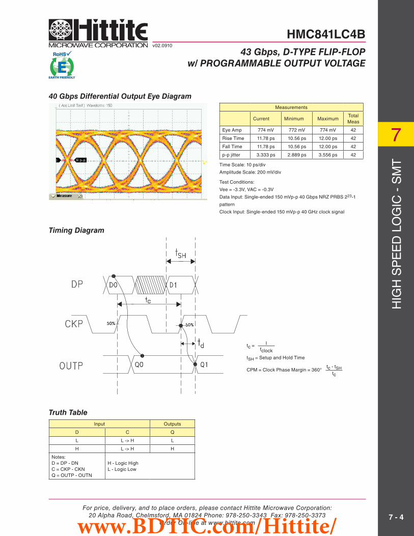
40 Gbps Differential Output Eye Diagram
Timing Diagram
Truth TableInput Outputs
D C Q
L L -> H L
H L -> H H
Notes:D = DP - DNC = CKP - CKNQ = OUTP - OUTN
H - Logic HighL - Logic Low
Ifclock
tc =
tSH = Setup and Hold Time
CPM = Clock Phase Margin = 360°tc - tSH
tc
Time Scale: 10 ps/div
Amplitude Scale: 200 mV/div
Test Conditions:
Vee = -3.3V, VAC = -0.3V
Data Input: Single-ended 150 mVp-p 40 Gbps NRZ PRBS 223-1
pattern
Clock Input: Single-ended 150 mVp-p 40 GHz clock signal
Measurements
Current Minimum MaximumTotal Meas
Eye Amp 774 mV 772 mV 774 mV 42
Rise Time 11.78 ps 10.56 ps 12.00 ps 42
Fall Time 11.78 ps 10.56 ps 12.00 ps 42
p-p jitter 3.333 ps 2.889 ps 3.556 ps 42
www.BDTIC.com/Hittite/
For price, delivery, and to place orders, please contact Hittite Microwave Corporation:20 Alpha Road, Chelmsford, MA 01824 Phone: 978-250-3343 Fax: 978-250-3373
Order On-line at www.hittite.com
HIG
H S
PE
ED
LO
GIC
- S
MT
7
7 - 5
Absolute Maximum Ratings
ELECTROSTATIC SENSITIVE DEVICEOBSERVE HANDLING PRECAUTIONS
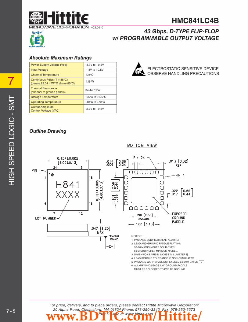
Outline Drawing
Power Supply Voltage (Vee) -3.7V to +0.5V
Input Voltage -1.3V to +0.5V
Channel Temperature 125°C
Continuous Pdiss (T = 85°C)(derate 29.04 mW/°C above 85°C)
1.16 W
Thermal Resistance(channel to ground paddle)
34.44 °C/W
Storage Temperature -65°C to +125°C
Operating Temperature -40°C to +70°C
Output Amplitude Control Voltage (VAC)
-2.3V to +0.5V
HMC841LC4Bv02.0910
43 Gbps, D-TYPE FLIP-FLOPw/ PROGRAMMABLE OUTPUT VOLTAGE
NOTES:1. PACKAGE BODY MATERIAL: ALUMINA
2. LEAD AND GROUND PADDLE PLATING:
30-80 MICROINCHES GOLD OVER
50 MICROINCHES MINIMUM NICKEL.
3. DIMENSIONS ARE IN INCHES [MILLIMETERS].
4. LEAD SPACING TOLERANCE IS NON-CUMULATIVE.
5. PACKAGE WARP SHALL NOT EXCEED 0.05mm DATUM -C-
6. ALL GROUND LEADS AND GROUND PADDLE
MUST BE SOLDERED TO PCB RF GROUND.
www.BDTIC.com/Hittite/
For price, delivery, and to place orders, please contact Hittite Microwave Corporation:20 Alpha Road, Chelmsford, MA 01824 Phone: 978-250-3343 Fax: 978-250-3373
Order On-line at www.hittite.com
HIG
H S
PE
ED
LO
GIC
- S
MT
7
7 - 6
HMC841LC4Bv02.0910
43 Gbps, D-TYPE FLIP-FLOPw/ PROGRAMMABLE OUTPUT VOLTAGE
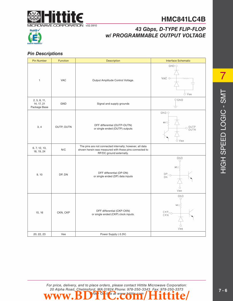
Pin Number Function Description Interface Schematic
1 VAC Output Amplitude Control Voltage.
2, 5, 8, 11, 14, 17, 21
Package BaseGND Signal and supply grounds
3, 4 OUTP, OUTNDFF differential (OUTP-OUTN) or single ended (OUTP) outputs
6, 7, 12, 13, 18, 19, 24
N/CThe pins are not connected internally; however, all data
shown herein was measured with these pins connected to RF/DC ground externally.
9, 10 DP, DNDFF differential (DP-DN)
or single ended (DP) data inputs
15, 16 CKN, CKPDFF differential (CKP-CKN)
or single ended (CKP) clock inputs.
20, 22, 23 Vee Power Supply (-3.3V)
Pin Descriptions
www.BDTIC.com/Hittite/
For price, delivery, and to place orders, please contact Hittite Microwave Corporation:20 Alpha Road, Chelmsford, MA 01824 Phone: 978-250-3343 Fax: 978-250-3373
Order On-line at www.hittite.com
HIG
H S
PE
ED
LO
GIC
- S
MT
7
7 - 7
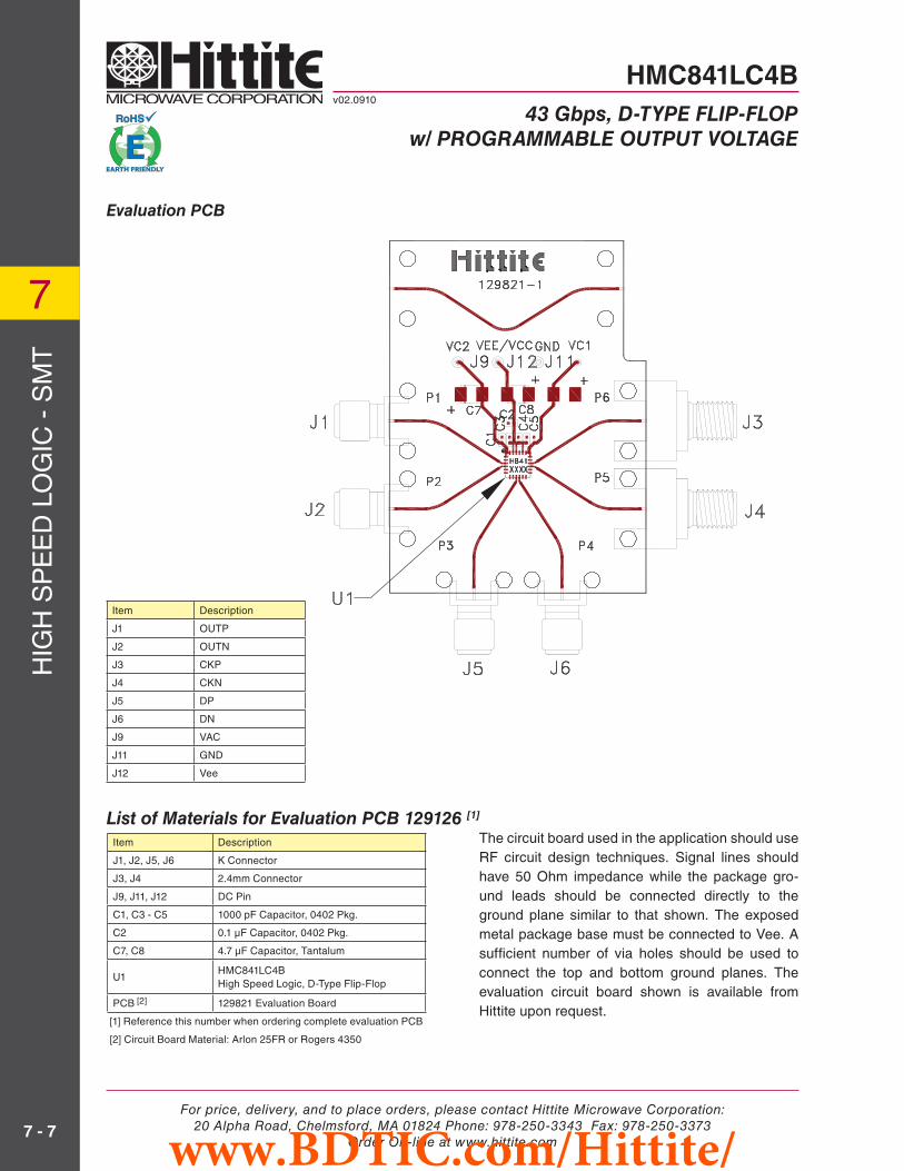
Evaluation PCB
HMC841LC4Bv02.0910
43 Gbps, D-TYPE FLIP-FLOPw/ PROGRAMMABLE OUTPUT VOLTAGE
List of Materials for Evaluation PCB 129126 [1]
Item Description
J1, J2, J5, J6 K Connector
J3, J4 2.4mm Connector
J9, J11, J12 DC Pin
C1, C3 - C5 1000 pF Capacitor, 0402 Pkg.
C2 0.1 µF Capacitor, 0402 Pkg.
C7, C8 4.7 µF Capacitor, Tantalum
U1HMC841LC4B High Speed Logic, D-Type Flip-Flop
PCB [2] 129821 Evaluation Board
[1] Reference this number when ordering complete evaluation PCB
[2] Circuit Board Material: Arlon 25FR or Rogers 4350
Item Description
J1 OUTP
J2 OUTN
J3 CKP
J4 CKN
J5 DP
J6 DN
J9 VAC
J11 GND
J12 Vee
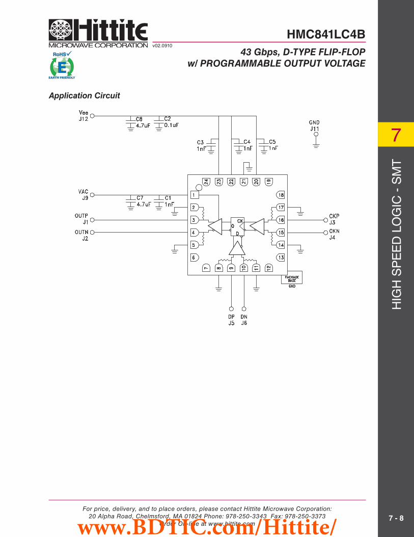
The circuit board used in the application should use RF circuit design techniques. Signal lines should have 50 Ohm impedance while the package gro-und leads should be connected directly to the ground plane similar to that shown. The exposed metal package base must be connected to Vee. A sufficient number of via holes should be used to connect the top and bottom ground planes. The evaluation circuit board shown is available from Hittite upon request.
www.BDTIC.com/Hittite/
For price, delivery, and to place orders, please contact Hittite Microwave Corporation:20 Alpha Road, Chelmsford, MA 01824 Phone: 978-250-3343 Fax: 978-250-3373
Order On-line at www.hittite.com
HIG
H S
PE
ED
LO
GIC
- S
MT
7
7 - 8
HMC841LC4Bv02.0910
43 Gbps, D-TYPE FLIP-FLOPw/ PROGRAMMABLE OUTPUT VOLTAGE
Application Circuit
www.BDTIC.com/Hittite/