Embed Size (px)
Citation preview

Doctoral School in Materials, Mechatronics
and Systems Engineering
THz Radiation Detection Based on CMOS
Technology
Moustafa Khatib
March 2019
30
th c
ycle

THZ RADIATION DETECTION BASED ON CMOS
TECHNOLOGY
Moustafa Khatib E-mail: [email protected]
Approved by: Prof. - - - - - - - - -, Advisor
Department of - - - - - - - - - University of - - - - - - - - -, Country.
Prof. - - - - - - - - -,
Department of - - - - - - - - - University of - - - - - - - - -, Country.
Ph.D. Commission: Prof. - - - - - - - - -,
Department of - - - - - - - - - University of - - - - - - - - -, Country.
Prof. - - - - - - - - -,
Department of - - - - - - - - - University of - - - - - - - - -, Country.
Prof. - - - - - - - - -,
Department of - - - - - - - - - University of - - - - - - - - -, Country.
University of Trento,
Department of Industrial Engineering (Materials, Mechatronics and Systems Engineering)
March 2019

University of Trento - Department of Industrial Engineering (Materials, Mechatronics and Systems
Engineering)
Doctoral Thesis
Moustafa Khatib - 2019 Published in Trento (Italy) – by University of Trento
ISBN: - - - - - - - - -

To my family and my friends


7
Abstract
The Terahertz (THz) band of the electromagnetic spectrum, also defined as sub-
millimeter waves, covers the frequency range from 300 GHz to 10 THz. There are
several unique characteristics of the radiation in this frequency range such as the
non-ionizing nature, since the associated power is low and therefore it is considered
as safe technology in many applications. THz waves have the capability of
penetrating through several materials such as plastics, paper, and wood. Moreover,
it provides a higher resolution compared to conventional mmWave technologies
thanks to its shorter wavelengths.
The most promising applications of the THz technology are medical imaging,
security/surveillance imaging, quality control, non-destructive materials testing and
spectroscopy.
The potential advantages in these fields provide the motivation to develop room-
temperature THz detectors. In terms of low cost, high volume, and high integration
capabilities, standard CMOS technology has been considered as an excellent
platform to achieve a fully integrated THz imaging systems.
In this PhD thesis, we report on the design and development of field effect transistor
(FET) THz direct detectors operating at low THz frequency (e.g. 300 GHz), as well
as at higher THz frequencies (e.g. 800 GHz – 1 THz). In addition we investigated the
implementation issues that limit the power coupling efficiency with the integrated
antenna, as well as the antenna-detector impedance-matching condition. The
implemented antenna-coupled FET detector structures aim to improve the detection
behavior in terms of responsivity and noise equivalent power (NEP) for CMOS based
imaging applications.
Since the detected THz signals by using this approach are extremely weak with
limited bandwidth, the next section of this work presents a pixel-level readout chain
containing a cascade of a pre-amplification and noise reduction stage based on a
parametric chopper amplifier and a direct analog-to-digital conversion by means of
an incremental Sigma-Delta converter. The readout circuit aims to perform a lock-in
operation with modulated sources. The in-pixel readout chain provides simultaneous
signal integration and noise filtering for the multi-pixel FET detector arrays and
hence achieving similar sensitivity by the external lock-in amplifier.

8
Next, based on the experimental THz characterization and measurement results of a
single pixel (antenna-coupled FET detector + readout circuit), the design and
implementation of a multispectral imager containing 10 x 10 THz focal plane array
(FPA) as well as 50 x 50 (3T-APS) visible pixels is presented. Moreover, the
readout circuit for the visible pixel is realized as a column-level correlated double
sampler. All of the designed chips have been implemented and fabricated in a 0.15-
µm standard CMOS technology. The physical implementation, fabrication and
electrical testing preparation are discussed.
Keywords
CMOS, Field-effect transistor, Terahertz radiation, Direct detectors, On-chip
antenna, Detectors, Readout circuit, Flicker noise, Responsivity, Noise
Equivalent Power, Incremental ADC, Chopper, Correlated Double Sampling,
Focal Plane Array (FPA), Multi-spectral Imaging.

9
List of Publications
Journal Articles
Conference Papers
M. Khatib, M. Perenzoni, “A Low-Noise Direct Incremental A/D Converter for FET-Based THz Imaging Detectors,” Sensors, 18 (6), 1867, June 2018.
M. Khatib, M. Perenzoni, “Response Optimization of Antenna-Coupled FET-based Detectors for 0.85 to 1 THz Imaging,” IEEE Microwave and Wireless Components Letters, Aug. 2018.
M. Khatib, M. Perenzoni, D. Stoppa” A Noise-Efficient, In-Pixel Readout for FET-based THz Detectors with Direct Incremental A/D,”47th Int. Conf. on ESSCIRC’17, Leuven, Belgium.
M. Khatib, M. Perenzoni, D. Stoppa” A CMOS 0.15-μm In-Pixel Noise Reduction Technique for Readout of Antenna-Coupled FET-based THz Detectors,”41st Int. Conf. on IRMMW-THz’16, Copenhagen, Denmark.
M. Khatib, M. Perenzoni, “Pixel-level Continuous-time Incremental Sigma-Delta A/D Converter for THz Sensors,” SPIE Photonics Europe 2016, Optical Sensing
and Detection, Brussels, Belgium.

10
Acknowledgements
It is quite incredible to look back and wonder how tough it would have been to
complete this thesis without the support and contribution of so many different people.
First and foremost, I would like express my sincere appreciation to advisor Mr.
Matteo Perenzoni for introducing me to the world of terahertz radiation and his
support and guidance all through this thesis project. He was always available to
discuss new ideas and the discussions with him have definitely shaped my approach
to solving problems. I am also deeply thankful to Dr. David Stoppa for giving me the
invaluable opportunity to be part of Integrated Radiation and Image Sensors (IRIS)
group in FBK and for allowing me to work on such a fascinating and challenging
project. I am thankful for his guidance and great support throughout at the beginning
of my PhD.
I would like to express my sincere gratitude to Dr. Nicola Massari for his guidance
and great support throughout my PhD. I enjoyed and learned much from the too
many interesting technical discussions that I had with him. I would also like to thank
Dr. Massimo Gottardi for the many great discussions in vision sensors and for
sharing his thoughts and experiences with me. He was always patient and
supportive whenever I had anything to discuss and was welcoming all the time. I
would like to thank Daniele Perenzoni and Daniele Rucatti for all their support with
the laboratory set-up during the chip measurements. I would like to thank Leonardo
Gasparini, Luca Parmesan and Manuel Moreno Garcia and all other new members
of the IRIS group for technical discussions and support.
I would like to thank Prof. Gian-Franco Della Betta and Prof. Lucio Pancheri of the
University of Trento for providing me with many different advanced courses in Image
Sensors and Microelectronics Devices which were valuable towards my
understanding of various concepts and motivated me to work in this direction.
Thanks for their continuous support throughout my PhD.
I wish to thank my colleagues Hesong Xu, Muhammed Ali and Olufemi Olumodeji for
providing me with invaluable help and technical support since the beginning of the
thesis. Their help was more than I could have asked for. I want also to thank my
colleagues during the last two years, with whom I shared conversations, ideas,
achievements, laughs and concerns, especially Majid Zarghami, Marco Zanoli,

11
Veronica Regazzoni, Chenfan Zhang and Matthew Franks, big thanks to all of you.
They made every day in the PhD office interesting and fun especially during the very
long nights of chip tape-out.
I also like to thank all my friends with whom I shared my life in Trento and for always
being so supportive, especially Ahmet Fadhil, Andrea Capuano, Abdallah Zeggada,
Boshra Khalaf, Leopoldo Gennaro Tripicchio, Andrea Moro, Giorgio Zanella. They
were like a family and made my stay enjoyable and full with happiness and fun.
Lastly, I would like to thank my family for their love and encouragement. Whatever I
have achieved in my life, I owe it to my mother and my sisters. They are the pillars
that I stand on today, always present even while on different continents. I am a better
person for I have them in my life.
Sincerely,
Moustafa Khatib

12
Table of Contents
Abstract .................................................................................................... 7 List of Publications .................................................................................... 9 Journal Articles ......................................................................................... 9 Conference Papers .................................................................................... 9 Acknowledgements ................................................................................ 10 List of abbreviation and acronyms .......................................................... 20 1 Introduction ........................................................................................ 23
1.1 Background ........................................................................................ 23 1.2 THz Radiation Properties ................................................................... 24
1.2.1 Non-ionizing ................................................................................. 24 1.2.2 Penetration .................................................................................. 25 1.2.3 High Resolution ............................................................................ 25 1.2.4 Atmospheric Effects ..................................................................... 27 1.2.5 Healthy-Safe Technology ............................................................. 28
1.3 THz Applications ................................................................................ 28
1.3.1 Security & Defence ...................................................................... 28 1.3.2 Biology and Medicine .................................................................. 29 1.3.3 Terahertz Spectroscopy ............................................................... 29 1.3.4 Quality Control and Non-Destructive Material Testing ............... 30 1.3.5 Communications .......................................................................... 30
1.4 Contributions of This Thesis ............................................................... 31 1.5 Organization of This Thesis ................................................................ 32
2 Terahertz Generation and Detection (State-of-The-Art)....................... 34
2.1 THz Sources ........................................................................................ 34
2.1.1 Free Electron Laser Based Sources (FEL) ...................................... 34 2.1.2 Backward-wave Oscillator (BWO) ................................................ 35 2.1.3 Gunn, IMPATT and TUNNEL diodes ............................................. 35 2.1.4 Frequency Multipliers .................................................................. 35 2.1.5 Optically Pumped Lasers (OPTL) .................................................. 35

13
2.1.6 Quantum Cascade Lasers (QCLs) ................................................. 36 2.1.7 Photomixers ................................................................................. 36
2.2 THz Detectors..................................................................................... 36
2.2.1 Golay Cell ..................................................................................... 37 2.2.2 Pyroelectric Devices ..................................................................... 38 2.2.3 Kinetic Inductance and Superconducting Detectors .................... 38 2.2.4 Bolometers .................................................................................. 38 2.2.5 Schottkey Barrier Diodes (SBDs) .................................................. 40 2.2.6 Field Effect Transistors (FETs) ...................................................... 41 2.2.7 Graphene-Based FET Detectors (GFET) ........................................ 41
2.3 THz Detection performance Parameters ........................................... 42
2.3.1 Responsivity (R) ........................................................................... 42 2.3.2 Noise Equivalent Power (NEP) ..................................................... 42 2.3.3 Detectivity (D*) ............................................................................ 43 2.3.4 Noise Equivalent Temperature Difference (NETD) ...................... 43
2.4 Chapter Summary .............................................................................. 43
3 On-Chip Terahertz Design Challenges and Detection Optimization ...... 46
3.1 Design Considerations in THz Detectors ............................................ 46
3.1.1 On-chip Terahertz Antenna ......................................................... 47 3.1.2 Power Coupling Efficiency ........................................................... 47 3.1.3 Signal/Noise Level Considerations ............................................... 48 3.1.4 Integrated Readout Design Considerations ................................. 48
3.2 FET THz Detector Model .................................................................... 48
3.2.1 Plasma Wave Theory ................................................................... 49 3.2.2 Self-mixing Principle .................................................................... 51
3.2.2.1 Quasi-Static Model ........................................................................ 51 3.2.2.2 Non-Quasi-Static (NQS) RC-ladder model .................................... 52
3.3 Geometrically Enhanced FET-based THz Detectors ........................... 54 3.4 THz On-chip Antenna Implementation .............................................. 55 3.5 Experiment Quasi-Optical Setup Description ..................................... 59
3.5.1 Impinging Input Power ................................................................ 61 3.5.2 THz Imaging Setup ....................................................................... 63

14
3.6 THz Characterizations and Imaging Results ....................................... 63
3.6.1 Low-frequency FET Detectors ...................................................... 63 3.6.2 High-frequency FET Detectors ..................................................... 65
3.7 Chapter Summary .............................................................................. 69
4 In-Pixel Low-Noise Readout Integrated Circuits ................................... 71
4.1 Motivation ......................................................................................... 71 4.2 Related Work ..................................................................................... 71 4.3 System-level Design ........................................................................... 72
4.3.1 Parametric Chopper Amplification .............................................. 74 4.3.2 Continuous-Time Incremental Conversion .................................. 76 4.3.3 CT Loop Filter ............................................................................... 78 4.3.4 Single-bit Quantizer ..................................................................... 80 4.3.5 Voltage DAC ................................................................................. 81
4.4 Readout Circuit Implementation ....................................................... 81 4.5 Chip Measurements ........................................................................... 83
4.5.1 Electrical Measurements of the Readout Chain .......................... 83 4.5.2 Antenna-Coupled FET Detector Measurements .......................... 86
4.6 Readout Responsivity and NEP Measurements ................................. 88 4.7 THz Imaging ....................................................................................... 90
5 Imaging Arrays and Multispectral Systems .......................................... 94
5.1 Motivation ......................................................................................... 94 5.2 Optimization of The THz Readout Chain ............................................ 94 5.3 Multispectral Imaging Architecture ................................................... 97 5.4 Visible Imaging Array ......................................................................... 99
5.4.1 3T- CMOS Active Pixel Sensor (3T-APS) ....................................... 99
5.4.1.1 Principle of Operation .................................................................... 99 5.4.1.2 Pixel Layout ................................................................................. 101
5.4.2 Column-level Correlated Double Sampling Readout Circuit ...... 101
5.4.2.1 OTA Design ................................................................................. 104 5.4.2.2 Simulation Results ....................................................................... 105 5.4.2.3 Layout of Column-level CDS ....................................................... 107
5.4.3 Auxiliary Blocks .......................................................................... 108

15
5.4.3.1 Bias Generation Circuits .............................................................. 108 5.4.3.2 Multiplexers .................................................................................. 109 5.4.3.3 Non-Overlapping Clock Generation Circuits ................................ 109 5.4.3.4 Column/Row Decoders ................................................................ 110 5.4.3.5 Output Buffers .............................................................................. 111
5.4.4 Chip Description ........................................................................ 115
6 Conclusions and Future Perspectives ................................................ 119 Appendix A: System-level Simulation: Matlab Simulink ........................ 122 Appendix B: Folded Cascode OTA Design Analysis ................................. 124

16
List of Tables
Table 2.1: Terahertz detectors performance comparison. ........................................ 44 Table 3.1: Performance comparison for the implemented FET detector structures. 69 Table 4.1: Performance comparison to the-state-of-the-art. ..................................... 92 Table 5.1: System-level specification of the folded cascode operational amplifier. 105 Table 5.2: Transistor sizes of the implemented operational amplifier. .................... 105 Table 5.3: Amplifier corners simulation results (AC analysis). ................................ 106 Table 5.4: Design specification of the two-stage Miller OTA. .................................. 111 Table 5.5: Transistors dimensions of the Miller OTA. ............................................. 111 Table 5.6: Amplifier corners simulation results (AC analysis). ................................ 113

17
List of Figures
Figure 1.1: Electromagnetic spectrum. ...................................................................... 23 Figure 1.2: Simple scheme of imaging system. ......................................................... 25 Figure 1.3: Atmospheric attenuation of the THz and IR spectrum. Adapted from [20].
.......................................................................................................................... 27 Figure 1.4: Samples THz images of different concealed objects obtained by a
security screening system. Adapted from [24].................................................. 28 Figure 1.5: Samples of visible and THz images of tissue diagnosis of human skin
using a TeraView system. Adapted from [26]. ................................................. 29 Figure 1.6: The current communication systems for human spaceflight missions at S-
band (2-4 GHz Ku (12-18 GHz), and Ka (26-40 GHz). Adapted from [36]. ...... 30 Figure 2.1: Cross-section and top view of Golay cell. adapted from [72]. ................. 37 Figure 2.2: Schematic of a simple bolometer. ........................................................... 39 Figure 2.3: Rectification behaviour of SBD coupled with an incident RF wave at zero
bias. .................................................................................................................. 39 Figure 2.4: Cross-section and top view of PGS SBD. Adapted from [88]. ................ 40 Figure 3.1: FET-based detection principle. ............................................................... 49 Figure 3.2: Schematic of FET-based detector. ........................................................ 50 Figure 3.3: FET-based NQS detection principle. ....................................................... 52 Figure 3.4: Layout view of the realized FET detector structures. .............................. 55 Figure 3.5: Design of the differential bow-tie antenna in the adopted 150-nm CMOS
technology. ....................................................................................................... 56 Figure 3.6: Simulation results of the antenna: antenna impedance in the frequency
range of 325 - 375 GHz. ................................................................................... 57 Figure 3.7: Antenna radiation efficiency and directivity in the range of 325 - 375
GHz. .................................................................................................................. 57 Figure 3.8: Simulation of the antenna radiation efficiency and directivity at 850 GHz,
900 GHz, and 1 THz. ........................................................................................ 58 Figure 3.9: Simulation of the input impedance of three antennas operating at 850
GHz, 900 GHz, and 1 THz. ............................................................................... 58 Figure 3.10: Chip micrograph (inset: terahertz pixel layout). .................................... 59 Figure 3.11: Picture of the experimental setup for the THz characterization. ........... 60 Figure 3.12: Block diagram of the THz characterization setup. ................................ 61 Figure 3.13: Measured input power of FET detector vs. signal frequency at distance
of 6 cm from the horn antenna. ........................................................................ 62 Figure 3.14: Block diagram of the THz imaging setup. ............................................. 63 Figure 3.15: Voltage responsivity versus signal frequency. ...................................... 64 Figure 3.16: Voltage responsivity versus gate bias voltage. ..................................... 64 Figure 3.17: NEP versus gate bias voltage. .............................................................. 65 Figure 3.18: Voltage responsivity versus signal frequency. ...................................... 66 Figure 3.19: Voltage responsivity versus gate bias voltage. ..................................... 67 Figure 3.20: NEP versus gate bias voltage. .............................................................. 67

18
Figure 3.21: Images of concealed metallic object inside a paper envelope: (a) a metallic ring captured by trapezoidal gate FET with 900 GHz antenna (fsrc =
910 GHz, Vgs = 0.46 V) (b) screw captured by extended drain FET with 1 THz antenna (fsrc = 1.02 THz, Vgs = 0.47 V). ........................................................ 68
Figure 4. 1: Block diagram of the proposed THz FET detector and readout structure. .......................................................................................................................... 73
Figure 4.2: 1/f noise and offset cancellation by using the parametric chopper amplifier. ........................................................................................................... 74
Figure 4.3: Gain and noise simulation results of the parametric amplifier at a chopping frequency of 100 kHz. ....................................................................... 75
Figure 4.4: Timing diagram of the THz readout chain. .............................................. 77 Figure 4.5: Schematic of the implemented decimator. .............................................. 77 Figure 4.6: Schematic of the pseudo-differential transconductor. ............................. 78 Figure 4.7: Schematic of the amplifier used in the Miller integrator. ......................... 79 Figure 4.8: Input referred noise voltage at three different configurations of the
readout. ............................................................................................................. 79 Figure 4.9: Schematic of the implemented single-bit quantizer. ............................... 80 Figure 4.10: Voltage DAC schematic. ....................................................................... 81 Figure 4.11: Layout view of the THz readout chain. .................................................. 82 Figure 4.12: Micrograph of the fabricated THz pixel structure. ................................. 82 Figure 4.13: Schematic of the PCB utilized for chip characterization. ...................... 83 Figure 4.14: Measured input noise power: without noise reduction (black), with the
conventional chopper technique (red) and with the proposed parametric chopper amplification (blue), chopping f = 100 kHz. ........................................ 84
Figure 4.15: Simulated and measured output signal PSD of the incremental sigma-delta converter tested with an input sinusoidal tone at 500 Hz and sampling rate 1 MHz. ....................................................................................................... 85
Figure 4.16: Noise PSD measured with shorted input to ground. ............................ 85 Figure 4.17: Measured FET voltage responsivity and Noise Equivalent Power (NEP)
versus gate bias voltage. .................................................................................. 86 Figure 4.18: Simulated and measured FET detector noise voltage spectral density
versus frequency. ............................................................................................. 87 Figure 4.19: Measured FET Voltage responsivity versus signal frequency. ............. 87 Figure 4.20: Readout responsivity as a function of FET gate bias voltage. .............. 89 Figure 4.21: Readout responsivity as a function of signal frequency. ....................... 89 Figure 4.22: NEP as a function of FET gate bias voltage (measured at 365 GHz). . 90 Figure 4.23: THz images of different metallic/plastic objects hidden inside a paper
envelope acquired at 365 GHz (source modulation f = 130 Hz) along with the photographs of the objects. .............................................................................. 91
Figure 5.1: Modified Schematic of the Miller Integrator. ............................................ 95 Figure 5.2: Layout view of the modified Miller Integrator. ......................................... 95 Figure 5.3: DC sweep simulation of the differential input versus the obtained
transconductance value at different source degenerated resistance values. .. 96 Figure 5.4: Multispectral imager architecture. ........................................................... 97 Figure 5.5: Timing diagram of the multispectral imager. ........................................... 98

19
Figure 5.6: Layout of single THz pixel with the readout chain, including also the visible pixel realized under the antenna’s ground plane and in the middle of the readout. ............................................................................................................. 98
Figure 5.7: Pixel schematic of a 3T-APS with the timing diagram. ......................... 100 Figure 5.8: Layout of a 3T-APS pixel. ..................................................................... 101 Figure 5.9: Operating principle of column CDS for visible pixel. ............................ 102 Figure 5.10: Transient simulation of the CDS with 3T-APS. ................................... 103 Figure 5.11: Current sweep simulation of visible pixel and CDS circuit. ................. 103 Figure 5.12: Schematic of folded cascode OTA of the column CDS for visible pixel.
........................................................................................................................ 104 Figure 5.13: AC simulations of Folded Cascode operational amplifier. .................. 106 Figure 5.14: Operational amplifier noise simulation. ............................................... 106 Figure 5.15: Layout of the column-level CDS readout circuit. ................................ 107 Figure 5.16: Bias voltages generation schematic.................................................... 108 Figure 5.17: Current mirror schematic for Gm cells and Miller integrator. .............. 108 Figure 5.18: Schematic of the multiplexer. .............................................................. 109 Figure 5.19: Schematic of the non-overlapped clock generator circuit. ................. 110 Figure 5.20: Schematic of the implemented row and column decoders. ................ 110 Figure 5.21: Transient simulation of the implemented row and column decoders. 110 Figure 5.22: Schematic of the output buffer (a), and the implemented Miller OTA (b).
........................................................................................................................ 112 Figure 5.23: The simulated open-loop frequency response of the Miller OTA. ....... 112 Figure 5.24: The simulated transient response of the Miller OTA in a buffer
configuration. .................................................................................................. 113 Figure 5.25: The simulated input noise of the Miller OTA. ...................................... 114 Figure 5.26: Layout of the output buffer using Miller OTA. ..................................... 114 Figure 5.27: Chip Layout including the core and the padring. ................................. 115 Figure 5.28: Chip micrograph (inset: terahertz pixel structure). ............................. 116 Figure 5.29: Schematic of the designed PCB testing board. .................................. 117 Figure 5.30: Layout of the designed PCB testing board. ....................................... 117

20
List of abbreviation and acronyms
Abbreviations
ADC Analog-to-Digital Converter
APS
Active Pixel Sensor
CDS Correlated Double Sampling
CMOS Complementary Metal Oxide Semiconductor
DN
Digital Number
ENOB Effective Number Of Bits
FET Field-Effect Transistor
FOM Figure Of Merit
FPA Focal Plane Array
GBW Gain-Bandwidth Product
LO Local Oscillator
NETD Noise Equivalent Temperature Difference
NQS Non-Quasi Static
PD Photodiode
RF Radio Frequency
SBD Schottky Barrier Diode
SD Sigma-Delta
SNR Signal-to-Noise Ratio
SOI Silicon On Insulator
TCR Temperature Coefficient of Resistance
THz Terahertz

21
Constants
Symbols Value Unit Description
𝜖𝑜 8.85419 × 10⁻¹² Fm−1 Permittivity of Vacuum
𝜖𝑜𝑥 3.9 Unitless Permittivity of Silicon Dioxide
𝜖𝑠𝑖 11.7 Unitless Permittivity of Silicon
𝑘𝐵 1.38 × 10⁻²³ JK−1 Boltzmann Constant
µ𝑛 250 − 1400 cm2V−1S−1 Electron Mobility
𝑞 1.6 × 10⁻¹⁹ C Elementary Charge
𝑡𝑜𝑥 2 nm Oxide Thickness
Variables
Symbols Unit Description
APyr cm2 Area of Pyroelectric Detector
Aeff cm2 Effective Area of Receive Antenna
Cox Fcm−2 Gate Oxide Capacitance per Area
D dBi Antenna Directivity
fs Hz Sampling Frequency
λ m Wavelength
∆f, B Hz Measurement Bandwidth
T K Temperature
f Hz Frequency

22
gm AV−1 Transconductance
gd S Conductance
ID A Drain Current
L m Channel Length
W m Channel Width
VGS V Gate-Source Voltage
VOV V Overdrive Voltage
VDS V Drain-Source Voltage
Vth V Threshold Voltage
NEP pW/√Hz Noise Equivalent Power
R Ω Resistance
Rv V/W Responsivity

23
1
Introduction
1.1 Background
The portion of electromagnetic (EM) spectrum located between the microwave and
infrared regions is defined as Terahertz (THz) band, as shown in Figure 1.1. It has
been recognized by several other terms, indicating either an electronic or an optical
approach. On the low frequency end, near the millimeter wave band, some authors
refer to the THz band basically as sub-millimeter band, (denoting to the wavelength),
some others refer to it with common terms such as gigahertz or far infrared [1], [2].
Still now, THz band does not have any industrial standard definition. Terahertz band
covers the region from 300 GHz to nearly 3 THz which corresponds to the
wavelength ranging from 1 mm (microwave) down to 0.1 mm (infrared) [3], [4]. While
certain applications such as THz spectroscopy and imaging are well established
(since the 1950s) [5], [6], however, up to recent times this band was not a matter of
much interest due to the difficulty of fabricating solid-state practical technologies for
sensing, generation, transmission of this radiation at room temperature.
Nevertheless, with the fast development in material science and standard fabrication
technology, numerous applications such as manufacturing, communications, security
and biomedical and materials/chemicals characterization are now appearing [7]–[11],
and the so‐called terahertz gap has emerged as a subject of great attention thanks
to its unique properties.
Figure 1.1: Electromagnetic spectrum.

24
Most of the already established THz designs and systems are typically based on
heavy bench-top instruments that have bulky size and high cost. Therefore, the
major direction of terahertz research and its apparatuses has recently focused
towards new concepts and new technologies for implementing both electronic
circuits and electromagnetic designs, that are capable of operating at specific bands
of this radiation providing high speed and being compact in size and power [12].
Terahertz technology is rapidly growing and extending the boundaries of
electromagnetic research for the optics and photonics communities. The recent
research was devoted to the development of terahertz sensors and detectors [13]–
[15]. THz radiation has many interesting and peculiar properties that mitigate some
of the disadvantages found in microwave and x-ray regions. By exploiting these
properties, the THz technology holds promise for unique and revolutionary
applications. In the next sections, some of the fundamental properties of THz
radiation are outlined, and their major fields of applications are reviewed.
1.2 THz Radiation Properties
Terahertz radiation has several specific properties, with respect to other portions of
the electromagnetic spectrum, and some of them are listed here below, to motivate
some perspectives for the consequent application section of this chapter:
1.2.1 Non-ionizing
Non-ionizing means that, in the considered wavelengths, the photon energy is low
and not sufficient to free electrons from atoms during irradiation. Electromagnetic
waves with shorter wavelengths such as ultraviolet, x-rays, and gamma rays are
ionizing radiation, whereas longer wavelength radiation such as visible, infrared,
microwaves, terahertz, and radio waves are non-ionizing (See Figure 1.1). Non-
ionizing radiation is preferred for bio-medical imaging applications since the waves
will not harmfully interfere with human DNA molecules and will not damage living
tissue. At 1 THz, the photon energies are estimated to be of the orders from 0.4 meV
up to 41.3 meV, as opposite to MeV levels at x-rays and therefore terahertz imaging
can be considered as more safer technology to be used in biomedical applications
[16].

25
1.2.2 Penetration
One of the key advantages of terahertz radiation is that it can penetrate through a
wide variety of non-polar and non-conducting (non-metallic) materials, including
plastics, paper, cardboard, clothing, etc.[17]–[19] due to the low water content,
particularly at frequencies below 1 THz. Therefore, terahertz radiation could be used
in imaging of concealed threats inside packages or under clothes, for security of
sensitive buildings such as airports and stations. Despite that, terahertz radiation is
still at an early stage of development and cannot replace the existing x-ray and mm-
wave imaging systems, since they offer superior performance with higher penetration
depth.
Figure 1.2: Simple scheme of imaging system.
1.2.3 High Resolution
A typical imaging system is composed of an optical system (lens, mirror, etc.) and a
focal plane imager (e.g. an array of detectors) as visible in Figure 1.2. Assume that
the optical system has a diameter D and a focal length fL while the scene is at a
distance L far from the optics.
The optics forms the image ab at the image plane of an object AB in the scene. If the
distance L > fL , the image plane is very close to the focal plane, i.e. fL ≈ 1, the
difference of incoming angle, for rays emitted respectively by points A and B, is
α =AB
L (1.1)
26
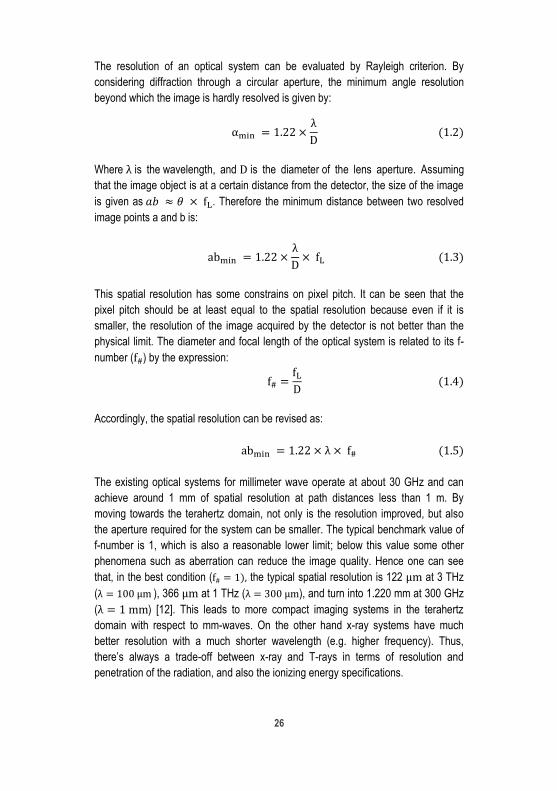
The resolution of an optical system can be evaluated by Rayleigh criterion. By
considering diffraction through a circular aperture, the minimum angle resolution
beyond which the image is hardly resolved is given by:
αmin = 1.22 ×λ
D (1.2)
Where λ is the wavelength, and D is the diameter of the lens aperture. Assuming
that the image object is at a certain distance from the detector, the size of the image
is given as 𝑎𝑏 ≈ 𝜃 × fL. Therefore the minimum distance between two resolved
image points a and b is:
abmin = 1.22 ×λ
D× fL (1.3)
This spatial resolution has some constrains on pixel pitch. It can be seen that the
pixel pitch should be at least equal to the spatial resolution because even if it is
smaller, the resolution of the image acquired by the detector is not better than the
physical limit. The diameter and focal length of the optical system is related to its f-
number (f#) by the expression:
f# =fL
D (1.4)
Accordingly, the spatial resolution can be revised as:
abmin = 1.22 × λ × f# (1.5)
The existing optical systems for millimeter wave operate at about 30 GHz and can
achieve around 1 mm of spatial resolution at path distances less than 1 m. By
moving towards the terahertz domain, not only is the resolution improved, but also
the aperture required for the system can be smaller. The typical benchmark value of
f-number is 1, which is also a reasonable lower limit; below this value some other
phenomena such as aberration can reduce the image quality. Hence one can see
that, in the best condition (f# = 1), the typical spatial resolution is 122 µm at 3 THz
(λ = 100 µm ), 366 µm at 1 THz (λ = 300 µm), and turn into 1.220 mm at 300 GHz
(λ = 1 mm) [12]. This leads to more compact imaging systems in the terahertz
domain with respect to mm-waves. On the other hand x-ray systems have much
better resolution with a much shorter wavelength (e.g. higher frequency). Thus,
there’s always a trade-off between x-ray and T-rays in terms of resolution and
penetration of the radiation, and also the ionizing energy specifications.

27
Figure 1.3: Atmospheric attenuation of the THz and IR spectrum. Adapted from [20].
1.2.4 Atmospheric Effects
Terahertz radiation suffers a severe atmospheric attenuation caused mostly by the
molecules of water and different particles. Conditions such as fog or dust cause a
strong attenuation and, as a result, it is impossible to perform measurements across
wide transmission windows for broadband applications, since the attenuation varies
with the signal frequency. Previous studies reported that propagation of radiation
over a distance more than 100 meters is almost impossible for frequencies from 1
THz up to 10 THz, even with a petaWatt of power [20]. Figure 1.3 displays a
comparison of the absorption coefficient of millimeter waves, THz, and IR waves at
sea level for different weather conditions. Under fog conditions, the THz absorption
near 240 GHz is around 8 dB/km. It is visible, above this frequency value and below
10 THz, the attenuation is mainly caused by atmospheric water vapor, with
attenuation due to rain and fog that have a heavy impact and can reach values
greater than 300 dB/km. It should be noted that the valleys between the peaks of
curves define the transmission windows of the atmosphere that should be used in an
imaging system to mitigate the propagation losses of the THz waves. Therefore, the
THz imaging is more desirable at low frequency than at high frequency in respect to
the signal losses caused by the atmospheric attenuation.

28
1.2.5 Healthy-Safe Technology
Originally, terahertz radiation has been considered as a completely safe radiation
because of its non-ionizing waves. However, this could not be truthfully the case,
since it’s a relatively recent topic of research and not yet completely verified against
prolonged exposure. Therefore, further investigations are required to define all of the
effects and resulting limitations in exposure, particularly with high power levels of
THz sources [21].
1.3 THz Applications
Over the past few years, terahertz technology has shown a great progress. Many
new advances in the realization of THz sources and detectors [22], [23] have
potentially opened up a wide range of applications, including explosive and
concealed threads detection, biomedical imaging, non-destructive testing, quality
control, and wireless communication systems [7]. Here, we briefly give an overview,
describing the capability of THz technology in those fields.
Figure 1.4: Samples THz images of different concealed objects obtained by a security screening system. Adapted from [24].
1.3.1 Security & Defence
THz technology can be utilized in security and military applications in a similar
fashion as x-ray screening, thanks to its ability to penetrate clothing and non-metallic
materials, and its high resolution. Airport gates and important buildings are good
examples of where terahertz security screening systems could be employed,
potentially detecting chemical and biological objects in a passenger's luggage or
concealed by a person [25]. Figure 1.4 shows different images of concealed
weapons obtained with a THz screening system.

29
Figure 1.5: Samples of visible and THz images of tissue diagnosis of human skin using a TeraView system. Adapted from [26].
1.3.2 Biology and Medicine
Biological and medical imaging is also one of the leading drivers of terahertz
technologies today [8], [27]. The key benefits arise from the non-ionizing nature of
the terahertz radiation making it a safe technology. Terahertz imaging has been
applied in analysing breast-tumours, cancer diagnosis in skin, liver and colon, in
addition to monitoring of biological tissue and healing of wounds. Figure 1.5 shows
samples of visible and THz images of tissue diagnosis of human skin using a
TeraView system [26].
1.3.3 Terahertz Spectroscopy
The principle of Terahertz Spectroscopy is based on the interaction between
electromagnetic radiations and a matter [28]. It allows, within one single experiment,
the determination of the opto-electrical properties of different materials over a wide
frequency spectrum ranging from 100 GHz up to several THz [29]. This information
can yield insight into material characteristics for a wide range of applications [8], [9].
Many different methods exist for performing THz spectroscopy such as: Fourier
transform spectroscopy (FTS) and narrowband spectroscopy are perhaps the most
common technique and widely used in passive systems for monitoring thermal-
emission lines of molecules, particularly in astronomy applications [30], [31] . A more
recent technique is named THz time domain spectroscopy (THz-TDS) [32]. THz-TDS
uses short electromagnetic waveforms produced by rectifying femtosecond optical
pulses, which are typically produced using ultrafast lasers. Beside THz spectroscopy,

30
there are many other spectroscopic techniques such as near infrared, Raman,
gamma, x-ray spectroscopy [33].
1.3.4 Quality Control and Non-Destructive Material Testing
Another important application of terahertz systems is quality control and non-
destructive testing [10], [34]. Terahertz systems can potentially be utilized for
inspections of manufacturing, fabrication process to guarantee product integrity and
reliability to preserve a uniform quality level [35]. Terahertz imaging has the potential
to detect component failures in semiconductors, plastics, or other material’s
manufacturing that would not be otherwise noticeable. Furthermore, it is possibly
feasible to characterise the properties, composition and impurities of substances,
overcoming the physical limitations and subjective judgement of humans.
Figure 1.6: The current communication systems for human spaceflight missions at S-band (2-4 GHz Ku (12-18 GHz), and Ka (26-40 GHz). Adapted from [36].
1.3.5 Communications
Nowadays, there are growing demands of using THz technology for wireless
communications [37], as the communication over THz carrier frequencies consent
overcoming the issues related to the lack of the available spectrum and can
potentially provide wider bandwidth (higher bitrates) with respect to lower
frequencies, and offering advantages over optical communication in satellite ground
link [13], [38]. However the challenge arises from the fact that THz radiation normally
has low power and suffer from high water absorption and other atmospheric effects,
therefore it get severely attenuated over long distances.

31
Space-based communications is another application for terahertz, since in a space
environment the atmospheric attenuation is not present [39]. The wider bandwidth of
a terahertz link could enable a higher bitrate between systems. Terahertz wireless
system gives the possibility to realize multi-gigabit throughput by fitting multiple GHz
channel bandwidth with reduced complexity system design and simple modulation
schemes compared to traditional spacecraft S-band, Ku-band, and Ka-band systems
(Figure 1.6).
1.4 Contributions of This Thesis
The main focus of this research is the development and characterization of CMOS-
based terahertz imaging systems. CMOS standard technology was adopted for the
implementation of different building blocks of the imaging focal plane arrays of
different chips such as antennas, detectors, readout circuits, thanks to its low cost,
scalability, commercial reliability, compact packaging, and low noise equivalent
power (NEP) that suit well the requirements of terahertz detection systems.
In an attempt to improve the terahertz detection behaviour in terms of responsivity
and NEP, geometrically enhanced FET-based detector structures are introduced.
The FET detector geometry and its parasitics play an important role on the power
coupling efficiency and the detector-antenna impedance matching conditions:
therefore, these FETs are integrated with several antennas operating at low
frequency range (325 - 375 GHz) as well as at the high frequency range (800 GHz -
1 THz), and are characterized in the same conditions for comparison. The design of
optimized antenna-coupled FET detectors was part of previous projects, while the
THz characterizations and testing have been performed during this thesis project.
The second chip contains a standalone readout chain having a size compatible with
the pixel available area, integrated with a FET-based THz detector operating in the
frequency range of 325 - 375 GHz, to process the detected signals. The
implemented readout circuit contains a cascade of a preamplification and noise
reduction stages based on a parametric chopper amplifier and a direct analog-to-
digital conversion (ADC) by means of an incremental ΣΔ converter, performing a
lock-in operation with modulated sources.
Then, the last chip contains 10 x 10 THz imager where each THz pixel is composed
of an on-chip antenna-coupled FET detector and a low noise readout circuit.
Moreover, visible pixels have been realized underneath the on-chip THz antennas
for the objective of realizing a multispectral imaging system. Each visible pixel

32
includes a photodiode and reset, select and source follower transistors, implemented
in 50 x 50 pixel array. Then, the visible pixels are readout by means of a column
level correlated double sampler and followed by an output buffer for processing the
signals. The main objective of the proposed imager architecture is to provide
simultaneous signal integration and acquisition of the entire pixel array, so as to
improve sensitivity, resolution or speed, and so to bring a further progress towards
high-performance terahertz imagers.
1.5 Organization of This Thesis
The thesis is organized as follows: Chapter 2 presents an overview of the state of
the art of terahertz sources and detectors that have been developed in literature over
the past years, describing their generation/detection capabilities and their
drawbacks. In particular, we emphasize FET-based detectors, as realized in this
work. Then, the conventional terahertz performance parameters are explained in
more detail.
In Chapter 3, the design challenges of the realization of terahertz imaging systems in
CMOS technology are discussed. Then, the chapter discusses the FET detection
principles that are presented in literatures including plasma wave theory and
distributed resistive self-mixing principles. Next, the analysis and design description
of optimized detector structures are presented. Afterwards, the chip implementation
and characterization and imaging setups along with the measurements and imaging
results are discussed.
Chapter 4 presents the system-level design considerations, followed by the principle
of operation, circuit analysis and simulation results of the low noise readout chain.
Then, the implementation of the terahertz pixel structure is explained. The electrical
characterization and terahertz measurements of the readout chain are then
discussed and validated the pixel performance.
In chapter 5, the design and implementation of a multispectral imager containing 10
x 10 THz pixels as well as 50 x 50 visible pixels is presented. The theoretical
analysis, simulations and characterizations of the imager architecture are also
presented in this chapter. Moreover, the physical implementation, fabrication and
electrical testing preparation are discussed.
Lastly, chapter 6 presents the conclusions and the discussion of future perspective
of this work.

33

34
2
Terahertz Generation and Detection (State-of-The-Art)
This chapter reviews techniques and systems of different types of terahertz sources
and detectors, realized in various technologies with their state of the art
performance. It gives an overview about basic concepts of operation and principles
to provide fundamental understanding of terahertz imaging systems. This chapter
also describes detection performance parameters for terahertz detectors.
2.1 THz Sources
Although THz band locates between infrared and microwave regions, none of the
signal generators in these two bands can simply be adapted for generation of THz
signals. The difficulty of realizing electronic THz sources with adequately high power
is due to the present limitations in conventional solid state electronic and
semiconductor devices. These basic building blocks are limited by reactive
parasitics, transit times that cause high-frequency roll-off or resistive losses that
control the device impedances at these wavelengths [40], [41]. Other issues such as
blocking, and heat dissipation significantly degrade the performance at high
frequencies near 1 THz. In this section, we briefly discuss the physical principles of
the widely used THz sources.
2.1.1 Free Electron Laser Based Sources (FEL)
Free electron lasers (FELs) have been known as light sources since 1960s: they can
operate without the use of an active laser medium except free electrons [42]–[44].
Technically, this makes them able to operate in any preferred wavelength range.
Their operation principle is based on the acceleration of the free electrons in vacuum
to a relativistic speed, and then decelerating these high speed electrons by moving
them through a magnetic structure such that they start to lose their energy which is
eventually converted into light. FELs sources show several advantages such as high
intensity and high power, easy tunability. FELs have shown their capability to the
applications such as spectroscopy, imaging, and material analysis.

35
2.1.2 Backward-wave Oscillator (BWO)
Backward wave oscillator (BWO) is a slow wave device, which operates based on
the interaction between an electron beam and a backward wave in the spatial
harmonics of a slow-wave structure [45]–[47]. BWO is considered to be a very
promising THz radiation source for many applications providing power levels in the
range of 1 - 100 mW with compact size, very reliable and can generate a CW signals
in the frequency range of 0.1–1.5 THz [48]. The main drawback of BWO is that it
requires an accelerating potential in the range 1 to 10 kV and an axial magnetic field
of about 1 T to achieve higher output power levels in the THz range.
2.1.3 Gunn, IMPATT and TUNNEL diodes
Gunn, IMPATT and TUNNEL diodes have been developed by several research
groups [49], [50]. They can be potentially used as an oscillator or amplifier in
applications that require relatively low-power radio frequency (RF) signals, such as
proximity sensors and wireless local area networks (LAN). These diodes have a
potential for compact and coherent terahertz sources operating at room temperature
and can generate a CW average power in the range of 0.1 - 1 mW around 400 GHz
through frequency multiplication with two or more diodes.
2.1.4 Frequency Multipliers
Frequency multipliers are principally realized to shift sub-terahertz electronic
oscillations into the terahertz range [51], where the fundamental RF frequency is
passed through a cascaded chain of doubler and triplers to reach the desired
frequency [52]–[54]. Most of frequency multipliers are balanced designs
implemented with monolithic circuits mounted in split waveguide blocks, offering
many advantages for generating terahertz waves such as high output power and
efficiency, low noise, electronic tuning and compact design. Yet, still, there is
considerable research work required for developing sources above 1 THz that have
high signal quality and electronic frequency tuning.
2.1.5 Optically Pumped Lasers (OPTL)
A carbon dioxide pump laser can generate several frequencies ranging from 300
GHz to 10 THz [55], [56], providing tens of milliwatts output power (typically 100
mW). However, they work at discrete frequencies, are bulky and require several tens
of watts of DC power. Accordingly, they are mainly limited to ground-based
applications where size and power are not matters. Despite the limited power, OPTL

36
are commercially available by several companies such as Coherent Inc. and
Edinburgh Inst.
2.1.6 Quantum Cascade Lasers (QCLs)
Quantum cascade lasers (QCL) are semiconductor laser sources for operating
wavelengths ranging from a few micrometers (μm) to well above 10 μm and into the
terahertz region. QCLs are designed such that the laser transitions are not between
different electronic bands (valence and conduction) but on inter-sub-band transitions
of the semiconductor structure. Those devices are designed to have a super-lattice
such that the probability of electrons are in varying energy locations that results in
splitting of a band into multiple permitted energies.
QCLs are realized in a compact size and provide mW output power range and able
to work in CW mode down to frequencies as low as 1.2 THz [57]–[59]. However,
QCLs have no real frequency tunability (temperature variation causes a shift of few
ppm) and need cryogenic cooling for maximizing the output power.
2.1.7 Photomixers
THz photomixers consists of the combination by heterodyning of two independent
tunable laser sources having frequency difference in a desired terahertz region [60],
[61]. The photoconductive antenna is the heart of photomixers [62], [63]. The
photoconductive antenna (PA) simply contains an electrical dipole on a high-mobility
semiconductor, fast enough to generate carriers in time with the beat frequency (e.g.
in order of picoseconds). Photomixers have many advantages such as operating in
CW mode, and being tunable; however, their output power in the 1 - 2 THz range is
at least of one order of magnitude lower than the power produced by room
temperature frequency multipliers.
2.2 THz Detectors
THz detectors are mainly based on three different physical principles, for example:
photodetection, thermal power detection, rectification [21]. At first, THz detectors can
be classified into incoherent (direct) and coherent (heterodyne) detectors [64], [65].
In incoherent detectors, only the signal intensity can be detected, whereas in
coherent detectors both the signal amplitude and phase are measured. Coherent
detectors provide a better noise performance by using heterodyning techniques[66],
37
[67]: the down-conversion of THz radiation is performed by mixing with a local
oscillation. Coherent detectors show good performance in terms of sensitivity and
responsivity, which makes these devices useful for spectroscopy applications [68].
On the other hand, direct THz detectors directly convert impinging THz radiation into
a baseband signal without any local oscillator. They typically provide modest
sensitivity and are well adequate for active imaging applications that require
moderate spectral resolution. An overview of the widely used THz direct detectors is
presented below.
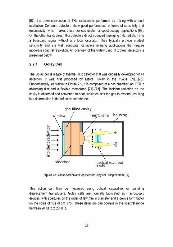
2.2.1 Golay Cell
The Golay cell is a type of thermal THz detector that was originally developed for IR
detection, it was first proposed by Marcel Golay in the 1940s [69], [70].
Fundamentally, as visible in Figure 2.1, it is composed of a gas chamber, an IR/THz
absorbing film and a flexible membrane [71]–[73]. The incident radiation on the
cavity is absorbed and converted to heat, which causes the gas to expand, resulting
in a deformation in the reflective membrane.
Figure 2.1: Cross-section and top view of Golay cell. adapted from [74].
This action can then be measured using optical, capacitive, or tunneling
displacement transducers. Golay cells are normally fabricated as macroscopic
devices, with apertures on the order of few mm in diameter and a device form factor
on the scale of 10s of cm [75]. These detectors can operate in the spectral range
between 20 GHz to 20 THz.

38
2.2.2 Pyroelectric Devices
Pyroelectric detectors are one of the most widely used thermal detectors for THz
radiation, thanks to their high sensitivity, compactness and wide apertures for
collecting the majority of power [76], [77]. These detectors contain a thin pyroelectric
film that act as a capacitor such that its capacitance value changes (e.g. since their
dielectric constant change) with respect to the temperature changes due to the
incident THz radiation on the pyrolectric device.
Therefore, by measuring the change of the current due to charging and discharging
of this capacitor, an estimated value of the incident power can be determined.
Pyroelectric detectors are sensitive only to heat (not wavelength), and therefore they
require a window material for wavelength selection. Pyroelectric detectors have the
advantages of being small, portable, exhibit a broad spectral response and they are
less expensive than Golay cells.
2.2.3 Kinetic Inductance and Superconducting Detectors
Kinetic inductance and superconducting detectors are playing an increasingly
important role in astronomy and biology [78], [79]. They can provide outstanding
sensitivity at cryogenic temperatures, operating in the frequency range of 1 - 2 THz.
However, there is still lack of accurate theoretical modeling which explains the
complex mechanism of different aspects of such detectors; but this does not prevent
researchers around the world from making experimental progress.
2.2.4 Bolometers
The micromachined bolometers are radiant-heat detectors [71], [72], which have
been widely used to detect wavelengths in the THz and IR bands. Bolometers are
composed of a temperature sensitive element that measures the increase of
temperature due to the incident electromagnetic power by detecting an electric
response (e.g. resistance change) [82], [83]. The sensing material that is utilized for
the bolometer has a large impact on the sensitivity of the detector. They are
implemented in a suspended bridge configuration for better thermal isolation with an
absorber made by a thin film semiconductor as visible in Figure 2.2. Their response
can be optimized through vacuum-packaging in order to cancel the losses caused by
air convection.

39
Figure 2.2: Schematic of a simple bolometer.
High performance bolometers need a temperature dependent material possessing a
large temperature coefficient of resistance (TCR), low noise, and moderate
resistance for reducing the mismatch with readout electronics input impedance.
Bolometers can successfully be integrated with a CMOS process technology through
a specialized process such as micromachining or above-IC wafer processing, and
therefore, it gives the possibility to implement FPAs with their respective readout
circuit [84]–[86].However, their main limitation is the high final cost, that includes
vacuum packaging.
Figure 2.3: Rectification behaviour of SBD coupled with an incident RF wave at zero bias.

40
2.2.5 Schottkey Barrier Diodes (SBDs)
The Schottky barrier diodes (SBDs) are semiconductor–metal junction diodes [87]–
[91]. In principle, as any kind of diode, their detection capability is based on the
strong nonlinear current–voltage characteristics as shown in Figure 2.3; the main
characteristics of SBDs with respect to the semiconductor junctions is the speed, so
they can rectify up to THz radiation. Recently, Poly-Gate-Separated (PGS) SBDs
were reported with measured cutoff frequency of 860 GHz [83].
Figure 2.4: Cross-section and top view of PGS SBD. Adapted from [92].
The cross section and top view of the PGS SBD fabricated in a 130-nm digital CMOS
process are presented in Figure 2.4. The SBDs feature a small junction capacitance
C and a low resistance R, therefore they have a small RC time constant. This leads
to fast response with a wide-bandwidth operation for THz rectification at room
temperature. This requires devices that are small (< 1μm x•1μm). Furthermore, for
more practical applications in THz imaging and sensing, to achieve a significantly
adequate resolution, a large array (100 × 100 elements may be required) of
detectors coupled with on-chip antenna elements is required. In most instances, a
major area is occupied by the antenna element on the wafer.

41
2.2.6 Field Effect Transistors (FETs)
Field-effect transistors (FET) have been exploited as direct detectors of THz
radiation, thanks to CMOS technology which offers the benefit of a standard
fabrication process with a high volume and the possibility of integration with readout
electronics, which is required for future large sensor arrays and terahertz (THz)
imaging systems. FET detector modeling is originally explained by the so-called
resistive mixer principle [93]–[98]. The incident radiation by the antenna is coupled
simultaneously to the gate and, through a gate-to-channel shunt capacitance, to the
drain terminal of the FET. Therefore, it generates a DC voltage, which is proportional
to the incident radiation power.
This phenomenon can be also explained by the plasma-wave rectification theory
proposed by Dyakonov and Shur [6], [100], as the FET channel can be considered
as a 2-D electron gas (2-DEG) with a hydrodynamic behavior similar to shallow
water, providing an effective power detection mechanism thanks to the nonlinear
characteristics of the FET. With the incident THz radiation, electron plasma waves
are excited in the transistor channel propagating with frequencies in the THz range
for short channel devices, and a voltage drop between the source and drain
terminals is induced. So far numerous configurations of FET detectors have been
developed, exhibiting good detection response and modest sensitivity at THz
frequency range [90]–[93]. Besides, grating-gate FET detectors ensure efficient
coupling with incoming terahertz radiation due to the interdigitated metal gates.
Hence they can provide much high responsivity than the standard FET detectors at
cryogenic temperatures [105].
2.2.7 Graphene-Based FET Detectors (GFET)
There is growing interest in utilizing graphene to implement FET detectors due to its
excellent electrical and mechanical properties [106]–[108], because of high intrinsic
carrier mobility and high carrier saturation velocity which open the possibility to
increase the operation frequency of the standard FET device in the THz range.
GFET operates as a typical FET detector according to the distributed resistive self-
mixing principle and it has a potential of increased sensitivity at room temperature
operation.

42
2.3 THz Detection performance Parameters
2.3.1 Responsivity (R)
THz detectors are basically characterized in terms of their responsivity (R) and their
noise equivalent power (NEP) that are evaluated with respect to the intensity of the
incident THz radiation. The responsivity evaluates the detector efficiency of
converting the impinging power into an electrical signal. It is defined as the voltage
(Vdet) or current (Idet) generated by a detector, normalized by the incident power
(Pin). It can be expressed as Eq. 2.2 for the voltage mode and as Eq. 2.3, for the
current mode, depending on which quantity is produced by the detector and the
employed readout technique. Therefore responsivity units are expressed in Volts per
Watt or Amperes per Watt.
RV =Vdet
Pin (2.2)
RI =Idet
Pin (2.3)
2.3.2 Noise Equivalent Power (NEP)
The noise equivalent power, which measures the detector sensitivity, denotes the
minimum detectable incident power in the system bandwidth. It is defined as the
root-mean squared (RMS) voltage (Vn) or current (In) intrinsic noise generated by
the detector in the system bandwidth divided by the voltage (RV) or the current
responsivity (RI). The NEP is given by Eq. 2.4 for the voltage mode and by Eq. 2.5
for the current mode operation.
NEPV =Vn
RV (2.4)
NEPI =In
RI (2.5)

43
2.3.3 Detectivity (D*)
D∗ represents the sensitivity per unit active area of a detector, which makes it easier
to compare the characteristics of different detectors. In many detectors, NEP is
proportional to the square root of the detector active area, so D∗ is expressed by the
following equation:
D∗ =√Adet B
NEP (2.6)
𝐷∗ was originally proposed for quantum detectors, in which the noise power is
always proportional to the detector sensitive area Adet and noise signal (Vn or In) is
proportional to the square root of the area, where B is the system bandwidth. Thus, a
larger value of D∗ indicates a better detection behaviour. The detectivity is given
as cm √Hz/W.
2.3.4 Noise Equivalent Temperature Difference (NETD)
An essential performance parameter for thermal detectors is the noise equivalent
temperature difference (NETD) that represents the minimum detectable temperature
difference (thermal resolution) over the system bandwidth. It is a figure of merit
related not only to the sensor but also depends on the employed optics. NETD also
relates to the NEP as it is stated in [109] and it is given by:
NETD =NEP∂Pd
∂T
× √B × 1 + 4f#
2
Adet (2.7)
where Pd is the power density emitted as blackbody radiation, T is the blackbody
temperature, f# is the focal ratio of the optics and depends on the ability of the lens
to collect light, given by Eq. 1.4 in the previous chapter.
2.4 Chapter Summary
This chapter presented the state of the art review of THz sources and detectors
realized in different technologies. In order to build an active imaging system, a
combination between source and detector is required, where the detection
performance can be less demanding by using a powerful source. The operation
principles of the widely used THz sources are described and their pros and cons in

44
terms of performance, area and power are discussed. Moreover, the structure of
each terahertz detector is described. In addition, some important figures of merits of
the detectors are given. Table 2.1 provides a performance comparison of the state of
the art THz detectors in terms of their operation frequency, speed, responsivity and
noise equivalent power.
Table 2.1: Terahertz detectors performance comparison.
THz
detector
Response
speed
Frequency
[THz]
Responsivity
[kV/W]
NEP
[𝐩𝐖 √𝐇𝐳]
Golay cell
Slow (50 ms)
0.04 – 30
10 – 100
140
Pyroelectric
detector
Slow (100 ms)
0.1 – 30
20 – 400
1000
Bolometer
Moderate
(1 ms)
0.1 – 30
100 – 1000
0.1
SBDs
Fast (20 ps)
0.1 – 10
1
1 – 50
FET
Fast
0.1 – 8
0.1 – 0.4
10 – 100
GFET
Fast
0.1 – 3
0.05 – 0.1
500 – 900

45

46
3
On-Chip Terahertz Design Challenges and Detection Optimization
This chapter present the main design considerations and integration challenges of
terahertz imaging systems based on CMOS process technology. Mainly, it focuses
on the design of antenna-coupled FET detectors, explaining the detection principles
in more details. Then, it describes detector’s design methodology, while being
compliant with process design rules imposed by the CMOS technology. Several FET
detectors are implemented with the aim of enhancing the detection sensitivity. The
first fabricated chip is described; in addition the characterization setups along with
the measurements results are discussed.
3.1 Design Considerations in THz Detectors
Despite most of the previously addressed THz detectors exhibit high sensitivity, they
are based on non-standard process technologies, which make it difficult to integrate
such detectors with signal processing circuits on a single chip. Some also require
specialized process steps, leading to complex fabrication processes. In addition,
some of them require cooling systems to maintain the cryogenic temperatures in
order to reduce the noise present in the device and detector circuit, which makes
them bulky, heavy and power hungry.
On the other hand, CMOS technology is the leading technology that can overcome
the abovementioned limitations. In recent years, significant progress has been
demonstrated with regard to CMOS based THz detectors. The advantages of CMOS
technology include a standardized fabrication process, low-cost, low-power, high
yield, and easy integration, simple digital interface, high speed, miniaturization, and
smartness via on-chip CMOS processing circuits.
In the previous chapter, among direct detectors, only SBDs and FETs have been
implemented in literature using CMOS process technologies. Therefore, the scope of
this work will be focused on CMOS based THz detectors and imagers. In particular,
we are more interested in studying THz radiation detection by means of an antenna-
coupled FET based THz detectors, since they are not limited by their cut-off

47
frequency, as in SBDs, due to the plasmonic behavior that takes place inside the
transistor’s channel enabling the THz detection. However, there are still many
challenges to be addressed with this approach, mainly related to the detected
signals characteristics. In the following paragraphs, these issues will be discussed.
3.1.1 On-chip Terahertz Antenna
The main bottlenecks of on-chip antenna are poor radiation efficiency and low gain
[110]–[112]. In typical CMOS process technology, the antenna can be built using thin
metal layers above a low resistivity silicon substrate (~1–10 Ω∙cm, εr = 11.7),
resulting in the majority of impinging power being coupled in the substrate, which
limits the performance of antennas. Additionally the implementation of the antenna-
coupled FET detector needs to meet the design density rules of the standard CMOS
process technology, and the dimensions of the antenna are directly proportional to
the wavelength of the radiation frequency.
3.1.2 Power Coupling Efficiency
The antenna impedance matching is challenging at terahertz frequency range since
the parasitic elements have significant impacts on the impedance values [113], [114].
For maximum power transfer, the FET input impedance and the antenna impedance
have to be conjugate match. According to [115], the FET responsivity (RV, V/W) is
highly dependent on the proper matching between the antenna impedance (ZANT)
and FET input impedance (ZFET), as expressed by:
RV = [4εradRe(ZANT) |ZFET
ZFET + ZANT|
2
] ∙1
4(Vgs − Vth) (3.1)
Here, εrad is the radiation efficiency, Vgs is the gate-to-source bias voltage and
Vth is the transistor’s threshold voltage. FET input impedance ZFET is typically
based on a combination of parasitic shunt capacitances and series resistances [108],
as described by:
ZFET = √Rds
j ω W L Cox//
1
j ω W L Cgs (3.2)
where, W, L are the device dimensions, ω is the frequency, Cox is the gate-to-
channel capacitance, and Cgs is the total gate-to-source capacitance. It can be noted

48
that the impedance has a capacitive behavior. The use of matching techniques is
extremely challenging at frequency near 1 THz due to the high losses of the
aluminum metal layers that form the antenna structure. Given that also the FET
impedance is frequency dependent, in order to achieve a proper impedance
matching, the antenna operating frequency can be tuned where it can achieve an
inductive part that conjugate-matches the capacitive part of the FET detector.
3.1.3 Signal/Noise Level Considerations
The higher signal-to-noise ratio (SNR) at the detector’s output, the better image
quality can be achieved. The SNR is typically determined by many factors such as:
the output signal intensity of the detector, electronic and environmental noise, and
the detector sensitivity. Within FBK’s THz experimental setup, typically the FET
detector’s signal intensity is of the order a few microvolts with a limited bandwidth,
since the frame rate goes from several tens of Hz to a few kHz in the case of THz
imaging applications. With this signal characteristic, the low-frequency flicker noise
severely influences the FET detector sensitivity and therefore degrades the SNR of
the imaging system. All these issues make the accurate measurements of FET
detector response extremely challenging.
3.1.4 Integrated Readout Design Considerations
Integrated readout circuits implemented in a noise-efficient way are expected to
provide a further progress towards a high-performance THz detectors and imagers
[116], [117]. Readout interfaces can be implemented at pixel level, column-level or
chip level. In this work we focus on pixel-level readout circuits. However, many
design constraints have to be considered. First, the readout interface must be
designed with an input referred noise specification well below the intrinsic noise of
the FET detector: to do so, the readout circuit should provide simultaneous signal
integration and noise filtering in order to preserve detection sensitivity [118], while
being capable to provide enough gain for the weak detected signal [119]. Secondly,
the readout circuit should use minimum area and power so that it can be scaled to
large imaging arrays.
3.2 FET THz Detector Model
The FET-based detection principle can be described by Figure 3.1. A FET-based
THz detector consists of a MOS field effect transistor acting as a rectifying element
which can detect the power of terahertz radiation received by the integrated antenna

49
and produces a proportional output DC voltage at the drain terminal. The gate is
biased with a sub-threshold voltage (VGS) in order to create a weak-inversion layer
from source to drain. FET detection operation can be explained with plasma wave
theory or the self-mixing effect.
Figure 3.1: FET-based detection principle.
3.2.1 Plasma Wave Theory
Plasma wave theory was first proposed by Dyakonov and Shur [6], [100] which
anticipated that a steady current flow in a FET channel can become unstable
bringing to generation of plasma waves, i.e. oscillations of electron density in space
and time. The possibility of detection is due to nonlinearities of the plasma waves
transfer in the transistor, since they can propagate in FET transistors with
frequencies higher than their intrinsic cut-off frequency.
When the THz radiation approaches to the transistor’s gate, the plasma oscillation
will be induced near the source and drain terminals in the two-dimensional electron
gas channel; as a result, a response to the terahertz radiation appears in the form of
a DC voltage generated between source and drain (VDS), which is proportional to the
radiation intensity. Typically this happens under certain a gate-to-source bias (VGS).
The FET can operate either in the resonant or non-resonant (over-damped) mode
depending on the angular frequency of the terahertz waves and the electron
relaxation time. In case of CMOS based THz detectors, the expected operation
mode is the non-resonant one due to the low electron mobility of silicon at room
temperature. The overdrive voltage VOV is the effective gate-to-channel voltage,
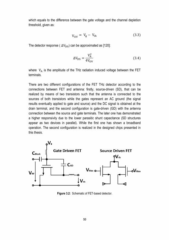
50
which equals to the difference between the gate voltage and the channel depletion
threshold, given as:
VOV= Vg − Vth (3.3)
The detector response ( ΔVDS) can be approximated as [120]:
ΔVDS = VA
2
4VOV (3.4)
where VA is the amplitude of the THz radiation induced voltage between the FET
terminals.
There are two different configurations of the FET THz detector according to the
connections between FET and antenna: firstly, source-driven (SD), that can be
realized by means of two transistors such that the antenna is connected to the
sources of both transistors while the gates represent an AC ground (the signal
results eventually applied to gate and source) and the DC signal is obtained at the
drain terminal, and the second configuration is gate-driven (GD) with the antenna
connection between the source and gate terminals. The later one has demonstrated
a higher responsivity due to the lower parasitic shunt capacitance (SD structures
appear as two devices in parallel). While the first one has shown a broadband
operation. The second configuration is realized in the designed chips presented in
this thesis.
Figure 3.2: Schematic of FET-based detector.

51
3.2.2 Self-mixing Principle
The FET THz detection principle has been also explained by the self-mixing theory in
a more circuit-focused understanding [121]. In this case, the FET device is
considered as a resistive mixer with a coupling capacitance between gate and drain.
According to the radiation frequency, the FET detection operation can be described
by either the quasi-static model or the Non-quasi-static (NQS) model. Both models
are briefly explained here below:
3.2.2.1 Quasi-Static Model
Quasi-static analysis can be primarily applied at low THz frequencies, where an
unbiased (cold) FET acts as a square-law power detector that can operate in both
saturation (active) or in triode (resistive) mode.
Figure 3.2 shows the schematic of the FET detector described by the resistive mixer
model.
The resistive mixing can be obtained by an external coupling capacitor between the
gate and the drain, providing a cross-modulation ( vgs(t) = vds(t) =
VRF sin(ωt). A dc gate-bias voltage VGS is also provided to control the channel
resistance. Therefore, the instantaneous value of the gate-to-source voltage is given
by:
vGS(t) = VGS + vgs(t) = VGS + VRF sin(ωt) (3.6)
Under the cold bias condition, the FET’s drain current ID is almost negligible,
therefore, the FET is considered to be operating in the linear region and can be
modelled as a voltage controlled current source in parallel with the drain-to-source
channel resistance, thus:
ids(t) = vds(t) × gds(t) (3.7)
Where gds(𝑡) is the FET’s drain-to-source conductance and can be written as:
gds(t) =W
LμCox (vgs(t) − Vth −
vds(t)
2) (3.8)
Where 𝑉𝑡ℎ is the threshold voltage, W and L are the FET’s width and length, μ is
the mobility and Cox is the oxide capacitance per unit area respectively. Therefore,

52
by substituting Eq. 3.8 into Eq. 3.7, the dc current response, which can be extracted
by neglecting the high frequency components at the drain terminal, can be calculated
as:
IDS = μCox
W
L(
VRF2
4) (3.9)
Therefore, the rectified DC output voltage can be written as:
VDS = (VRF
2
4VOV) (3.10)
This low-frequency analysis is further generalized by a non-quasi-static description.
Figure 3.3: FET-based NQS detection principle.
3.2.2.2 Non-Quasi-Static (NQS) RC-ladder model
The simple Quasi-static analysis of square-law FET power detector is only valid in
the low frequency range near RF and microwave frequencies, where the distributed
nature of the device can be neglected. At higher frequencies, this model
underestimates the effects of device parasitics and therefore, it has to be replaced
by a non-quasi-static (NQS) distributed principle, which is also known as distributed
resistive self-mixing. In this model, both the external gate-to-drain coupling capacitor
at low frequencies and the non-quasi-static effects at terahertz frequencies are taken
into consideration.

53
The FET THz detector will be operated above its typical cut-off frequency, where the
non-quasi-static effects of the device can be considered by dividing the channel into
segments, where each segment is short enough so that the ordinary quasi-static
transistor equations can be used, as shown in Figure 3.3. Each segment Δx is
utilized by a variable conductance gN(v) that is controlled by the gate-to-channel
voltage v(n) and the segment capacitance equivalent Cn,ox to the fraction of the
total gate-to-channel capacitance Cox. Therefore the unit capacitance is given by:
Cn,ox = W Δx Cox (3.11)
The unit conductance depends on the conductivity “G” which is related to the
channel length segment Δx and the time t.
gN(v) =G(v(Δx, t))
Δx (3.12)
The model can be analyzed as an RC-transmission line, where each segment of the
RC-ladder resembles a square-law mixer. Therefore, for infinitesimally short
transistor segments, this leads to a partial differential equation as follows:
∂
∂x[G(v(x, t) − Vth)
𝜕v(x, t)
∂x] = CoxW
∂
∂xv(x, t) ( 3.13)
Numerical solutions of Eq. 3.13 reveal strong cross-modulation response near to the
gate-source contact with an exponential roll-off along the channel. It can be
observed that each segment of the NQS model resembles the simple self-mixing
power detector circuit, such that the distributed intrinsic gate-channel capacitance
Cox does the same impact as the external coupling capacitor Cgd in the low-
frequency quasi-static situation.
The short channel FETs are expected to achieve better detection performance well
above the transistor cut-off frequency as described by the distributed resistive self-
mixing principle, since shorter devices achieve higher self-mixing modulation
efficiency due to lower parasitic capacitances as well as less parasitic resistance
from the non-modulated part of the channel. FET terahertz detection has been
described by other several models such as [122] presented a FET model based on
EKV FET model. Other work presented a SPICE model based on distributed RC
circuit; however the paper does not address the effect of non-zero drain–source
current [123].

54
3.3 Geometrically Enhanced FET-based THz Detectors
The main advantages of exploiting antenna-coupled FETs as THz power detectors is
the use of CMOS standard fabrication process, providing a compact solution for the
implementation of a complete THz imaging systems, in addition to the possibility of
integrating readout circuits for processing the detected signals. The FET detectors
can be easily implemented in a pixel array and the detection performance can be
potentially optimized by changing the device dimensions (W, L), offering more design
flexibility.
Previous studies attempted to optimize the FET detection response through utilizing
different technologies and devices, for example using a Silicon lens with back-side
illumination [124], in order to enhance the detector efficiency. Other research
realized the FET detector in Silicon-on-isolator (SOI) CMOS technology [125], which
offers lower parasitics of the detector devices improving the sensitivity, but it has the
drawbacks of having thinner dielectrics and metals in its back-end, and much
stringent metal-density rules. This makes difficult to achieve high-efficiency
antennas, degrading the system performance. So far, little efforts have been
invested in optimizing the detection behavior with respect to the geometrical
configuration of the FET detector.
The geometry of FET transistor has a strong impact on the effects of its parasitics. It
should be noted that the use of deep-submicron FET transistors is expected to
improve the detection and lower the noise through efficient modulation of the
channel; however this results in higher intrinsic thermal noise of the device due to
the higher channel resistance. On the other hand, the use of FET transistor with
larger dimensions has, indeed, a lower thermal noise contribution; however this has
an opposite impact on the antenna-FET matching due to larger gate capacitance.
Therefore, for the sake of preserving good detection behavior for the FET detector,
while improving the power coupling with the integrated antenna and its impedance-
matching restrictions, two different FET structures called trapezoidal gate FET (Trap)
and extended source FET (Ext), are implemented in a gate-driven configuration as
visible in Figure 3.4. In addition, Regular FET (Reg) has been realized for
performance comparison. The trapezoidal FET is designed with the purpose of
reducing the channel resistance through expanding the drain access conductance,
and thus reducing the NEP while keeping a minimum gate-to-source overlap
capacitance. The extended FET aims to reduce the parasitic capacitance between
the polysilicon gate and the source metal contact by extending the diffusion of the
source side further away, hence facilitating higher response. It should be noted that

55
these structures are realized without affecting the antenna-FET impedance matching
since the transistor width is unchanged at the source contact.
Figure 3.4: Layout view of the realized FET detector structures.
3.4 THz On-chip Antenna Implementation
The structure of the on-chip antenna can significantly affect the performance of the
FET detector. As a result of the reported challenges of THz antenna design there
were many CMOS integrated antennas are proposed for THz imaging systems, such
as bow-tie antennas [126], ring antennas [127], planar dipole antennas [128] and
patch antennas [129]. In this work we implemented a bow-tie antenna structure due
to its higher efficiency since the larger width reduces resistance and therefore it has
smaller losses. Moreover it is easier to satisfy metal coverage rules as the antenna
area is larger.
Different antennas have been designed to operate in the frequency range of 325–
375 GHz as well as at higher frequencies 850 GHz, 900 GHz and 1 THz. The bow-tie
antenna is designed according to the methodology described in [130]. Figure 3.5
describes the antenna structure with the metal stack of the CMOS technology. The
adopted CMOS process provides six metal layers, with a thick metal option,
sandwiched between layers of a dielectric with a relative permittivity (
ϵr = 4.1 ). The bow-tie antenna is built by top thick metal layer (MT), while the
bottom layer M1 is utilized as a ground plane in order to shield the substrate and
avoid the losses caused by the surface waves,
The dielectric height from the ground plane to the bow-tie is approximately 7 μm.
The remaining layers (M2 – M6) are used as square dummy patches to achieve the
required metal density in order to meet the process design rules of CMOS
technology. Furthermore, the top thick metal layer (MT) is compliant with the foundry
rules without any dummy because of antenna arm structures.

56
Figure 3.5: Design of the differential bow-tie antenna in the adopted 150-nm CMOS technology.
The gate and source terminals of the FET detector are directly connected to the
differential antenna through stacked metal vias with minimum dimensions (0.24 μm),
also the FET is designed with minimum dimensions (W/L = 0.32 μm/0.15μm) in
order to reduce the inductance of this connection lines that could affect the FET-
antenna impedance matching. The 300 GHz antenna cell dimensions are 456 x 320
μm2, while the antenna dimensions are 200 x 200 μm2 for the frequency range 850
GHz - 1 THz. The 300 GHz antenna was designed as a square cell in a previous
chip by modifying the dimensions of the ground plane to be 456 x 456 μm2.
The antenna performance has been validated through CST Microwave studio EM
simulations. In order to transfer the maximum power, the antenna impedance and
the FET impedance have to be a complex conjugate pair. According the model
described in [115], the FET impedance is evaluated based on the process
parameters of the utilized CMOS technology. The antenna impedance (ZANT)
versus the signal frequency is plotted in Figure 3.6, indicating ZANT = (146 + 497j) Ω
at a frequency of 325 GHz and hence there is anyway non-optimal antenna-FET
impedance matching at a certain frequency that gives a peak response at the
desired frequency range. As is visible in Figure 3.7, the achieved radiation efficiency
is in the range of 26 – 33% from 325 to 375 GHz with a range of directivity of 4.5 –
5.1 dBi. In fact, the obtained efficiency is low due to the thin dielectric layer between
the bow-tie and the ground plane, in addition to the conductor and dielectric losses at
this frequency range. However, the simulations did not show any side lobes due to
the surface waves, thanks to the reflector.

57
Figure 3.6: Simulation results of the antenna: antenna impedance in the frequency range of 325 - 375 GHz.
Figure 3.7: Antenna radiation efficiency and directivity in the range of 325 - 375 GHz.
At higher terahertz frequencies the radiation efficiency is better compared to the 300
GHz antenna due to the fact that the ground plane is further away in relative terms
with respect to the signal wavelength, and therefore the response is not canceled out
by the mirror currents induced in the same ground plane. However, the impedance
matching with the FET detectors became more challenging. Figure 3.8 shows the
simulation results of the radiation efficiency, which is around of 58% with peak
directivity range of 4.2 – 5 dBi over the frequency range of 0.85 – 1.1 THz for three
different antennas, while Figure 3.9 shows the simulated antenna impedance.

58
Figure 3.8: Simulation of the antenna radiation efficiency and directivity at 850 GHz, 900 GHz, and 1 THz.
Figure 3.9: Simulation of the input impedance of three antennas operating at 850 GHz, 900 GHz, and 1 THz.
Figure 3.10 shows the chip micrograph of multiple antenna-coupled terahertz
detectors arranged in a pixel array for both 300 GHz (upper part) and 850 GHz – 1
THz pixel (lower part) structures with a zoom in the layout design of one of the pixels.
The proposed detector consists of an NMOS field effect transistor with non-biased
channel as rectifying element, an integrated on-chip bow-tie antenna, where each
pixel can be addressed individually. The antennas are only different in the
dimensions of the bow-tie in order to operate at different radiation frequencies. THz

59
detector structures are realized in LFoundry 0.15-μm standard CMOS technology
and fulfill all the technological constraints and reliability rules.
Figure 3.10: Chip micrograph (inset: terahertz pixel layout).
In this implementation the different antennas are properly sized and optimally
matched in simulations for each of the selected frequencies to achieve a proper
coupling with the FET detectors at the corresponding radiation frequencies. In fact,
we built different high frequency FETs (e.g. 850, 900, 1000 GHz) in order to verify
that in the whole range a comparable detection performance could be achieved
similar to the low frequency detectors (e.g. 300 GHz) implemented in the same die.
3.5 Experiment Quasi-Optical Setup Description
The THz measurements were performed with two different setups using CW THz
sources that can cover the low frequency range of 270 – 380 GHz as well as the
high frequency range of 850 GHz – 1 THz. The THz source is based on a frequency
multiplier chain driven by a synthesizer (8 – 20 GHz) with a diagonal horn antenna to
transmit the signal in the free space. The multiplier chain contains several doublers
and triplers that can be installed to generate a THz signal in the desired frequency
range. Figure 3.11 shows a picture of the characterization setup.

60
Figure 3.11: Picture of the experimental setup for the THz characterization.
Figure 3.12 shows the configuration of the quasi-optical setup for the THz detectors
characterization. The FET voltage response is recorded by using a lock-in amplifier
(AMETEK 7265) with time constant of 200 ms. Typically, the lock-in sensitivity is
chosen based on the FET signal intensity, which is related to the characteristics of
emitted THz radiation ( e.g. frequency and power). The THz source and the lock-in
amplifier are electronically chopped at near 1 kHz by using a function generator, so
as to reduce the 1/f noise and the dc-offset. The maximum allowed chopping
frequency is limited to 1 kHz: in this way the low-pass filter given by the lock-in
amplifier input capacitance and the FET’s RDS do not influence the measurement. A
user-controlled attenuation (UCA) switch is used for background subtraction.
Therefore, additionally to the modulation, the data provided by the lock-in amplifier is
further processed calculating the difference between the FET signal acquired with
the THz source on and off (completely attenuated output signal). In this way, any
coupling or interference due to an electromagnetic induction are removed. The
measurements were performed in normal ambient air at room temperature.

61
Figure 3.12: Block diagram of the THz characterization setup.
3.5.1 Impinging Input Power
According to the measurement methodology described in [131], to estimate the
impinging power on the THz test structure, the voltage response of a calibrated
reference detector (e.g. pyroelectric device) placed at the same distance from the
horn antenna is measured. The pyroelectric detector sensitive area was delimitated
by a pin-hole with 2 mm diameter so as to reduce the radiation reflections effects
inside the metal cylinder attached at the pyroelectric input.
The pyroelectric power density is evaluated by dividing the measured voltage
response by its responsivity which is given by the manufacturer. Then, the impinging
power received by the FET-based THz detector structure could be obtained as the
power density of the pyroelectric detector multiplied by the antenna effective
area Aeff, as given by:
Aeff = D λ2
4π (3.14)
where D is the antenna directivity, and λ is the wavelength of the THz signal.
Multiplier chain (0.85 – 1.1 THz) (265 – 375 GHz)
THz FPA
Control and Acquisition
Board
Lock-in Amplifier
(AMETEK 7265 )
Function Generator
UCA
fmodfmodFrequency Synthesizer
VDI 8-20 GHz
Horn Antenna
Zeonex Lens

62
Figure 3.13: Measured input power of FET detector vs. signal frequency at distance of 6 cm from the horn antenna.
The impinging power delivered to the FET detector is estimated as:
PFET = (VPyro
Rpyro ) (
Aeff
APyro) (3.15)
here APyro, VPyro and Rpyro are the pyroelectric sensitive area, the measured
pyroelectric voltage response and its responsivity respectively. By using this method,
the estimated input power is independent on transmitter specifications. It is
necessary to consider that the diffraction and reflection effects in the measurement
setup could result in responsivity and NEP values characterized by minima and
maxima, which are largely different than the actual detector performance. Therefore,
these non-realistic values should be removed by smooth averaging of the measured
data. The measured input power received by the THz detector as a function of signal
frequency is presented in Figure 3.13, where the resulting averaged curve is also
shown. The impinging power received by each pixel is around 100 – 200 nW over
the frequency range of 260 – 370 GHz. Similarly, the impinging power is about 8 –
35 nW for the frequency range from 850 GHz to 1 THz.

63
3.5.2 THz Imaging Setup
The experimental setup for performing THz imaging acquisition is built as presented
in Figure 3.14. The object to be imaged is vertically positioned in the focal point
between two Zeonex lenses with 25 mm focal length, such that the THz beam is
focused on the object by the first lens and collimated by the second lens and then
refocused on the test chip. Since our chip sensor contains only a single pixel, a
mechanical scanning is necessary to obtain a wide field of view. Therefore, a stepper
motor is equipped to scan the image objects in the vertical and horizontal directions
by a step size equals to the single pixel pitch (e.g. 0.2 mm for 850 GHz pixels or 0.4
mm for 300 GHz pixels). In each motor step, part of the image object is registered by
the pixel until the complete image is formed.
Figure 3.14: Block diagram of the THz imaging setup.
3.6 THz Characterizations and Imaging Results
3.6.1 Low-frequency FET Detectors
In order to characterize the low frequency FET detectors, the tunable CW source has
been configured to generate terahertz signals in the range between 265 – 375 GHz,
while the lock-in amplifier is configured with time constant of 500 ms and sensitivity
of 100 μV, since the FET detector output signal is expected to be in the order of few
μV. Firstly, the voltage response of each FET detector is normalized by the received
input power in order to evaluate the responsivity. Voltage responsivity of the FET
THz detector versus signal frequency is shown in Figure 3.15. In this measurement,
Multiplier chain (0.85 – 1.1 THz) (265 – 375 GHz)
THz FPA
Control and Acquisition
Board
Lock-in Amplifier
(AMETEK 7265 )
Function Generator
UCA
fmodfmodFrequency Synthesizer
VDI 8-20 GHz
Horn Antenna
Zeonex Lens
Zeonex Lens
Stepper motor
Image Object

64
the THz source frequency was swept, while the gate bias voltage VGS was kept fixed
at the optimal bias point for all the three FET structures.
Correspondingly, Figure 3.16 shows the measured responsivity as a function of FET
gate bias voltage where the peak response of each FET is near the FET threshold
voltage. The measurements are obtained at modulation near 1 kHz.
Figure 3.15: Voltage responsivity versus signal frequency.
Figure 3.16: Voltage responsivity versus gate bias voltage.
The NEP of the FET detector depends on the thermal noise voltage, which depends
on the FET intrinsic resistance Rds. The intrinsic resistance can be measured using
a multimeter and its noise density can be measured by a spectrum analyzer. Then,

65
the NEP of the detector is obtained as a ratio between thermal noise voltage of the
channel resistance and its voltage responsivity. The measurement result of the NEP
for the different structures is shown in Figure 3.17. Minimum NEP is 185 pW/√Hz at
380 GHz was obtained by the trapezoidal gate FET at 0.48 V. It is possible to see
that both extended source and trapezoidal gate detectors considerably achieved
better detection behavior than the regular one.
Figure 3.17: NEP versus gate bias voltage.
3.6.2 High-frequency FET Detectors
Similarly to low-frequency FET detectors, the THz characterization setup has been
modified to test similar FETs operating in the frequency range of 850 GHz – 1 THz.
Figure 3.18 shows the measured responsivity as a function of signal frequency,
calculated as the FET voltage response normalized by the received power of each
pixel. It can be seen that the peak responses of the three bow-tie antennas are
slightly shifted to 885 GHz, 910 GHz, and 1.02 THz instead of 850 GHz, 900 GHz,
and 1 THz respectively. This shift in frequency is possibly due to the imprecision of
the electromagnetic simulator, and to the uncertainty of thicknesses and material
properties (e.g. skin effect of CMOS metal layers in the THz frequency range). In this
measurements, trapezoidal FETs always achieve higher response than the extended
FET that can be understood as a higher self-mixing efficiency thanks to the improved
asymmetry of the structure (see Figure 3.4). Indeed, the parasitic capacitance Cgd is
larger and its impedance lower (1/jωCgd), so as the gate and drain are effectively
shorted. Therefore, a higher voltage signal vds(t) ≈ vgs(t) = VRF sin (ωt) will be
transferred to the drain, resulting in higher DC current Ids = ⟨vds(t) × gds(t)⟩ as

66
given in Eq. 3.9 of the simple self-mixing model. Similar considerations hold also for
the NQS model. Hence, this result in higher detected output voltage as it is given by
the DC current multiplied by the DC output resistance, and therefore higher
responsivity.
Figure 3.18: Voltage responsivity versus signal frequency.
Similarly, the extended FET demonstrates an improvement in responsivity which is
due to the lower overall Cgs, thanks to the farther source connection, effectively
decreasing the fringe capacitance between polysilicon and metal. In fact, the
reduction of this parasitic decreases the signal attenuation due to the shorting path
that prevents the power coupling to the FET channel (see Eq. 3.2). Measurements
on 850 GHz antennas indicate a peak RV of 235 V/W and 211 V/W for trapezoidal
and extended FETs respectively. With 900 GHz antennas, the responsivity drops
slightly near 200 V/W for both FET structures.
At 1 THz, the detectors achieve peak RV of 157 V/W and 143 V/W for trapezoidal
and extended FETs respectively. It can be observed that the proposed FETs provide
a RV higher than the regular one in all three antenna designs, showing a
reproducible and consistent advantage. The responsivity measurements versus Vgs
are obtained by tuning the THz source at fsrc = 885 GHz, 910 GHz, and 1.02 THz.
As visible in Figure 3.19, the RV raises in the weak inversion and peaks
approximately near the threshold voltage of the different FET structures.

67
Figure 3.19: Voltage responsivity versus gate bias voltage.
In accordance with the initial design considerations, the trapezoidal FET realizes a
lower thermal noise voltage (1.67 μVrms at Vgs = 0.46 V) than the extended FET
(1.98 μVrms at Vgs = 0.47 V), since the enlarged access region at the drain side of
the trapezoidal FET gives a lower Rds , accordingly improving the NEP. The
measured NEP versus Vgs is illustrated in Figure 3.20: the minimum NEP of the
trapezoidal FET is 187 pW/√Hz measured at Vgs = 0.46 V and fsrc = 885 GHz, while
the minimum NEP of the extended FET is 249 pW/√Hz obtained at Vgs of 0.47 V and
fsrc = 910 GHz. Both proposed FETs show a considerably better NEP than the
regular one, with the trapezoidal FET having an advantage of simultaneously
improving voltage response and thermal noise, as explained before.
Figure 3.20: NEP versus gate bias voltage.

68
(a)
(b) Figure 3.21: Images of concealed metallic object inside a paper envelope: (a) a metallic ring captured by trapezoidal gate FET with 900 GHz antenna (fsrc = 910 GHz, Vgs = 0.46 V) (b) screw captured by extended drain FET with 1 THz antenna (fsrc = 1.02 THz, Vgs = 0.47 V).
Under continuous terahertz illumination, metallic objects including a nut and a screw
concealed inside a paper envelope are mechanically scanned by using a stepper
motor with a resolution of 0.2 mm. Figure 3.21 displays two different images scanned
at 910 GHz and 1.02 THz with trapezoidal gate and extended source FETs
respectively, in a single-pixel mode. The dynamic range of the present imaging
system is approximately 48 dB; the images result a bit defocused due to limited
output power from the THz source and the struggle in tuning the optics distance with
such a weak signal and a single-pixel operation. The scanned area is 20 x 20 mm2
reaching a final image resolution of 100 × 100 pixels.
Table 3.1 provides a performance summary and comparison of both low-frequency
and high frequency FET THz detector structures. Both are fabricated and tested
under the same conditions. The characterization results of the modified FET
structures show values in line with typical performance that can be found in
literature. In addition both of the modified detectors provide higher RV and lower NEP
over the regular structures at no additional cost in terms of cost, complexity and
area.

69
Table 3.1: Performance comparison for the implemented FET detector structures.
Frequency
[THz]
Max. 𝐑𝐕
[V/W]
Min. NEP
[pW/Hz1/2]
Reg
0.38 131 342 @ Vgs = 0.48 V
0.85 171
268 @ Vgs = 0.48 V 0.9 116
1 112
Trap
0.38 218 216 @ Vgs = 0.5 V
0.85 235
187 @ Vgs = 0.46 V 0.9 200
1 157
Ext
0.38 239 210 @ Vgs = 0.5 V
0.85 211
249 @ Vgs = 0.47 V 0.9 200
1 143
3.7 Chapter Summary
In this chapter, the design considerations and challenges of developing FET based
THz detectors have been addressed. Moreover, the FET detection mechanisms by
means of plasma wave theory and self-mixing principles have been discussed. The
second part of this chapter presented the implementation of several THz pixel
prototypes operating at both 265 – 380 GHz as well as 850 GHz – 1 THz frequency
range. The FET detectors have been implemented in a 0.15-µm standard CMOS
technology and experimentally characterized in terms of responsivity and NEP. At
low radiation frequency, trapezoidal gate FET achieved a peak responsivity of 218
V/W and minimum NEP of 216 pW/√Hz, while extended source FET obtained a peak
responsivity of 239 V/W and minimum NEP of 210 pW/√Hz. Even when operating at
frequencies near 1 THz, responsivity measurements on the proposed FET structures
stay in the range of hundreds of V/W without degrading the performance, similar to
the low-frequency FET detectors. At high frequency, the best performance is also
achieved by the trapezoidal gate FET with 850 GHz antenna, with a peak
responsivity of 235 V/W, and minimum NEP of 187 pW/√Hz, validating the improved
power coupling efficiency between the antennas and FET detectors.

70

71
4
In-Pixel Low-Noise Readout Integrated Circuits
4.1 Motivation
In the previous chapter, different FET structures were analysed through THz
measurements so as to improve responsivity and noise performance when they are
used as THz detectors in multi-pixel array: however, the weak-detected signal from
the FET still needs to be processed. As an alternative to the lock-in techniques, an
in-pixel readout circuit can provide simultaneous readout of multiple pixels,
integrated functionalities, and a compact system. In the literature, only few
representative design examples are reported. Therefore, this chapter discusses the
design considerations for readout circuit implementation including the following: 1) a
sufficient amplification of the weak detected signal by the FET, 2) the low frequency
1/f noise and offset reduction techniques, 3) a small power consumption of the
readout circuit, with area compatible with the physical size of antenna.
Correspondingly, in order to achieve these objectives, a low-noise readout interface
circuit is designed, built, and tested. According to the obtained THz characterization,
a comparable detection performance to the state of the art designs is achieved. The
proposed readout circuit has demonstrated the capability of preserving the minimum
NEP of the FET detector at room temperature, while providing a direct digital output
as a representation of the detected signals.
4.2 Related Work
In an attempt to enhance FET detector sensitivity, several approaches are reported
in the literature for the implementation of the readout interface. In [129], a 3 x 5 FPA
for imaging at 650 GHz has been introduced, with a readout circuit featuring a
differential amplifier, which was a cause of significant noise and thus degraded the
system performance. Besides, THz characterization of such an FPA is still
dependent on using the lock-in technique to acquire raster-scanned THz images with
very slow frame rates.

72
The work in [127] presented an architecture for a FET-based 1-k pixel camera for
video imaging. In this architecture, an integration capacitor of 8 pF per pixel is
utilized to decrease the integrated noise by reducing the system cut-off frequency,
but still not filtering all the noise down to the video rate signal bandwidth.
Another work in [132] efficiently addressed the noise filtering by realizing a
demodulation chain based on high-Q Switched-Capacitor (SC) filtering. However, the
1/f noise reduction always depends on the possibility of modulating the THz source
at hundreds of kHz, which is not a cost-effective solution for a THz imaging system.
A more recent work in [103], presented an FPA for imaging at 860 GHz, integrated
with a single-readout chain comprehending a cascade of a chopper instrumentation
amplifier and a sigma-delta ADC. Although the achieved THz performance
parameters by the proposed imaging system, the large area of the readout circuit
makes it not being compact to be fully integrated inside each pixel for simultaneous
readout of multi-pixel imaging arrays. Besides, the power consumption is expected to
be large due to the noise constraints with such a complex readout structure.
In FBK Integrated Radiation and Image Sensor group, several THz readout circuits
were proposed before. In [119], [133] an implementation of a readout interface based
on a switched-capacitor integrator is fabricated in a 0.13-μm standard CMOS
technology for THz imaging applications. [117] presented A THz pixel architecture
implemented in a 0.15-μm CMOS technology and consists of a 370 GHz on-chip
antenna, a FET-based THz detector and a chopper-stabilized switched-capacitor
multistage readout interface performing in-pixel filtering and amplification.
4.3 System-level Design
Figure 4.1 illustrates the block diagram of the FET-based THz detector circuit
integrated with the readout chain. The FET THz detector is realized by two NMOS
transistors in a gate-driven structure: one of them is connected to the integrated
antenna, acting as an active FET THz detector, rectifying the incident radiation. The
second NMOS is acting as a blind detector, providing a reference device for offset
compensation of the differential input pair, and therefore, only the voltage difference
between the two detectors is amplified. The two FET detectors are biased with the
same gate voltage.

73
Figure 4.1: Block diagram of the proposed THz FET detector and readout structure.

74
The integrated readout chain contains a cascade of a preamplification and noise
reduction stage based on a parametric chopper amplifier and a direct analog-to-
digital conversion by means of an incremental sigma-delta converter, followed by a
decimation stage that provides a 12-bit digital output as a measure of the intensity of
the rectified FET signal. Initially, several high-level Matlab simulations were
performed to scale the coefficients of the CT loop transfer function and to determine
the design values that make sure the precise incremental ADC operation can be
achieved. A Simulink model of the readout circuit design and the transient simulation
results can be found in Appendix A.
4.3.1 Parametric Chopper Amplification
The operation principle of the parametric amplifier is schematically simplified in
Figure 4.2. The parametric amplifier operates in a discrete-time mode, containing two
sampling switches followed by two MOS varactors [134]. This amplification technique
has the advantage of being noise-free with low power consumption [135]. The
realized gain is basically given as the ratio of the small-signal gate capacitances of
the MOS varactors during alternating the signals Clks and Clkboost in two non-
overlapped clock phases. The parametric amplifier is enclosed in between the
chopper modulators that operate at a frequency of fch, which equals half of the
operating frequency of the parametric amplifier. Therefore, they eliminate the 1/f
noise from the signal path simultaneously along with reducing the thermal noise
during the sampling and the boost phases of the parametric amplifier.
Figure 4.2: 1/f noise and offset cancellation by using the parametric chopper amplifier.

75
The value of the passive gain is approximately 2–3, reducing the overall input
referred thermal noise contribution of the readout chain. Figure 4.3 illustrates the
simulations of the gain and noise of the chopper parametric amplifier, executed by
Parametric Steady-State, AC and Noise (PSS/PAC and PNOISE) analyses. The
simulations demonstrate a small noise contribution of 9 nV/√Hz dominated by only
thermal noise with a passive voltage gain of 2.3 at a chopping frequency of 100 kHz.
Three choppers are placed around the parametric amplifier and the transconductors
in the feed-forward and feedback paths to reduce 1/f noise and the DC-offset. Only
the feed-forward path is considered in Figure 4.2. The first chopper at the input
modulates the FET signal, which is located at the source modulation
frequency fmod, to the odd harmonics of the chopping frequency fch. Then, the
modulated signal together with 1/f noise and the DC-offset are converted into current
by the Gm stage of the incremental ADC. After that, the last chopper at the
transconductor output demodulates the signal back to fmod and shifts the 1/f noise
and the offset to the odd harmonics of chopping frequency, such that they will be
filtered out by the loop filter realized with a Miller integrator. All the switches in the
chopper modulators are realized with a complementary transmission gate with
minimum transistor dimensions, to reduce the chopper spikes produced by the
charge injection during the switching between the two clock phases.
Figure 4.3: Gain and noise simulation results of the parametric amplifier at a chopping frequency of 100 kHz.

76
4.3.2 Continuous-Time Incremental Conversion
Incremental sigma-delta (SD) Analog-to-Digital Converters (ADCs) benefit from the
oversampling and noise shaping techniques with relaxed matching requirements
similar to traditional SD ADCs [136]. The use of incremental SD operation in the THz
detection context has the advantage of simultaneously integrating the rectified FET
signal and averaging the detector noise, providing a one-to-one mapping between
the FET signal and the digital output per each conversion cycle [137]. In this design,
a first order modulator structure is realized, as it offers a medium resolution (i.e.,
more than 10 bits) that fulfils the requirements of THz imaging applications, without
increasing the complexity in both the analog loop filter and the digital decimator
[138]. Higher order modulators are avoided, due to their limited stability and higher
power consumption. A Continuous-Time (CT) loop filter based on a Gm-C structure
has been implemented, since it accommodates smaller settling and bandwidth
requirements when compared to the switched-capacitor counterpart, and hence, it
achieves lower power consumption [139].
The operating principle of the readout chain can be explained in the conceptual
timing diagram of Figure 4.4. The CT loop filter and the decimator are reset at the
beginning of each conversion cycle (Tconv). Then, the slowly varying FET voltage
signal (VFET) is continuously integrated and sampled for an integration period of Tint
= 2n Tqnz, where n is the converter resolution and Tqnz is the sampling period. In
each period of Tqnz, the integrator output voltage is compared to the quantizer
threshold and a decision is made. Next, according to the quantizer decision, the
voltage DAC feeds back either a +VREF or a -VREF signal to the input of the feedback
transconductor; as a result, the up-down digital counter, which is realized as a
decimator, will either increment or decrement its digital value. At the end of Tconv,
the integrator output voltage can be described by:
Vint = Gmin
CintTqnz [2n VFET −
Gmfb
Gmin
(Nup − Ndown) VREF] (4.1)
where Cint = C1 + C2, Gmin and Gmfb are the integrating capacitor and
effective transconductance values in the feed-forward and feedback paths,
respectively. Nup and Ndown are the number of subtractions and additions of VREF
respectively.

77
Figure 4.4: Timing diagram of the THz readout chain.
The Least Significant Bit (LSB) resolution is thus defined by VREF scaled by the ration
of the transconductance values in the feed-forward and feedback paths, as well as
the number of clock cycles per one conversion as given by:
VLSB = (Gmin
Gmfb
)VREF
2n (4.2)
Lastly, the digital counter value is extracted through a parallel-to-serial shift register
and a new conversion cycle starts with cleared counter. A digital modulator is
inserted between the quantizer and the counter: it operates at the same frequency of
the source fmod, thus, permitting the measurement of the pixel output in both
conditions (source on/source off) in order to compute the difference between them in
similar way to the lock-in technique. Figure 4.5 shows the schematic of the
implemented decimator.
Figure 4.5: Schematic of the implemented decimator.

78
4.3.3 CT Loop Filter
The transconductors (Gm stages), depicted in Figure 4.6, are designed using a
pseudo-differential source degeneration topology with resistors acting as
transconducting elements [140]. In principle, the follower transistors (M1–M2)
transfer the input voltage to the resistor, consequently improving the linearity in the
V-I conversion. Then, the current mirrors (M3–M6) transfer the currents to the
outputs.
Thus, the effective Gm value will be approximately equal to 1/R. PMOS transistors
operating in weak inversion were used for the input differential pair due to their lower
1/f noise contribution and to allow the use of near-ground input common-mode
specified by the FET voltage signals. All the other transistors are sized to have a
long channel length and operated in strong inversion such that the noise should be
only dominated by the input pair.
The output currents from the Gm cells are added/subtracted and then injected into a
Miller integrator [141], such that the effect of finite output impedance at the
transconductors’ outputs is reduced. The amplifier utilized in the Miller integrator is
composed of a current buffer common-gate input followed by a common-source
stage as visible in Figure 4.7. The bias current in the Gm stages and the Miller
integrator, which sets the noise floor of the incremental ADC, is 4 µA, resulting in a
total current dissipated in the incremental loop filter of 24 µA.
Figure 4.6: Schematic of the pseudo-differential transconductor.

79
Figure 4.7: Schematic of the amplifier used in the Miller integrator.
According to [142], the chopping frequency is chosen to be several times greater
than the flicker noise corner (which is around 10 kHz, as obtained from the noise
simulation), to effectively shift the 1/f noise out of the signal band and then it will
filtered out by the loop filter of the incremental ADC. The integrating capacitors are
implemented as Metal-Insulator-Metal (MIM) capacitors, while high-resistivity
polysilicon is used for realizing the degeneration resistors.
The readout channel has been analysed using periodic analysis (PSS, PAC and
PNOISE) in Cadence. Figure 4.8 shows the simulated input referred noise voltage
spectral density in three different configurations for the readout channel: without
chopper modulator, with chopper modulator only active and lastly with parametric
amplifier + chopper modulator active.
Figure 4.8: Input referred noise voltage at three different configurations of the readout.
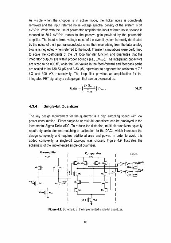
80
As visible when the chopper is in active mode, the flicker noise is completely
removed and the input referred noise voltage spectral density of the system is 81
nV/√Hz. While with the use of parametric amplifier the input referred noise voltage is
reduced to 50.7 nV/√Hz thanks to the passive gain provided by the parametric
amplifier. The input referred voltage noise of the overall system is mainly dominated
by the noise of the input transconductor since the noise arising from the later analog
blocks is neglected when referred to the input. Transient simulations were performed
to scale the coefficients of the CT loop transfer function and guarantee that the
integrator outputs are within proper bounds (i.e., ±VREF). The integrating capacitors
are sized to be 800 fF, while the Gm values in the feed-forward and feedback paths
are scaled to be 130.33 µS and 3.33 µS, equivalent to degeneration resistors of 7.5
kΩ and 300 kΩ, respectively. The loop filter provides an amplification for the
integrated FET signal by a voltage gain that can be evaluated as:
Gain = (2Gmin
Cint) TConv (4.3)
4.3.4 Single-bit Quantizer
The key design requirement for the quantizer is a high sampling speed with low
power consumption. Either single-bit or multi-bit quantizers can be employed in the
incremental Sigma-Delta ADC. To reduce the distortion, multi-bit quantizers typically
require dynamic element matching or calibration for the DACs, which increases the
design complexity and requires additional area and power. In order to avoid this
added complexity, a single-bit topology was chosen. Figure 4.9 illustrates the
schematic of the implemented single-bit quantizer.
Figure 4.9: Schematic of the implemented single-bit quantizer.

81
It is based on the structure presented in [143], containing a pre-amplifier stage to
avoid the kick-back noise [144], followed by a positive feedback latched comparator.
The implemented comparator is designed with minimum transistor dimensions,
except for the bias transistor Mtail.
4.3.5 Voltage DAC
The voltage DAC schematic is shown in Figure 4.10. The quantizer will give an output
of 1-bit digital value as input to the DAC. Then, the DAC converts the 1-bit digital to
an analog signal and feeds it to the input of the feedback transconductor. The
corresponding analog output signal from the DAC will also have two levels (+VREF, –
VREF). If the output of the quantizer is high, the DAC will generate positive reference
voltage )+VREF( to the input of the feedback transconductor and in case of zero
digital input to the DAC, the analog output will be a negative reference voltage )–
VREF(. The voltage VREF is set to a value that guarantees the integrator outputs are
within a proper bound.
Figure 4.10: Voltage DAC schematic.
4.4 Readout Circuit Implementation
Figure 4.11 shows a layout view of the THz readout chain. The most sensitive blocks
to parasitic elements and transistors mismatch are the Miller integrator and the pre-
amplifier inside the quantizer. Therefore, in order to reduce the parasitic
capacitances and resistances, and to improve the matching in the transistor pairs
with equal size, the layout of these amplifiers have been done following the well-
known techniques that minimize gradient induced mismatches [145], [146].

82
The main techniques that are used in the readout design are common-centroid
layout and inter-digitization are considered as in [147]. The transistor array are made
as compact as possible in order to make it less subject to nonlinear gradients. All
transistors must be oriented in the same direction, which means that they need to be
parallel to each other in order to avoid transconductance variations. Other related
points include avoiding routing metal across the active gate area. In addition,
decoupling capacitors are distributed over the channel to filter supply noise.
Moreover, in order to avoid any coupling between digital and analog blocks of the
chip, the analog areas are isolated from the digital logic by use of guard rings. For
the same reason, separate supply and ground lines are used for digital and analog
supplies.
Figure 4.11: Layout view of the THz readout chain.
A micrograph of the readout chain with THz antenna and FET detector is shown in
Figure 4.12. The design has been fabricated in a 150-nm standard CMOS
technology. The total area of the readout chain is 90 x 300 µm2. Two identical
readout circuits are fabricated: one of them is integrated with the antenna-coupled
FET THz detector, and the other is for the purpose of performing an electrical test for
the readout circuit operation. Table 4.1 provides information about pin numbering,
pin names, type and direction.
Figure 4.12: Micrograph of the fabricated THz pixel structure.

83
4.5 Chip Measurements
The test of the THz pixel structure is performed in two steps: firstly, the electrical
testing of the readout circuit operation is performed, by using external input signals
generated by a function generator. After that, a similar THz characterization setup as
in Figure 3.12 is built to characterize a standalone FET detector and to validate the
antenna operating frequency by using a lock-in amplifier. Lastly, the integrated
readout chain is used in place of the lock-in amplifier so as to measure the FET
signal in a digital representation. Figure 4.13 shows the schematic of the PCB board,
where it can be seen both analog and digital signals that can be taken off-chip for
test and debugging purposes for the test structure.
Figure 4.13: Schematic of the PCB utilized for chip characterization.
4.5.1 Electrical Measurements of the Readout Chain
The measurement of the input-referred noise power is carried out in three different
configurations of the THz readout chain as visible in Figure 4.14. The noise
measurements were acquired at the CT loop filter output, while the differential input
pins are shorted to ground. Then, it is divided by the expected closed-loop gain (see
Eq. 4.5) in order to be referred to the input of the readout chain. The noise
measurements are obtained at a chopping frequency of 100 kHz to effectively
eliminate the 1/f noise and the DC-offset in the signal bandwidth. It is clear that the
flicker noise is dominant at low frequency when the choppers are not active. In the
second case, the parametric amplifier is bypassed and only the conventional
chopper technique is presented to eliminate the flicker noise and hence only the
thermal noise remains in the signal bandwidth.
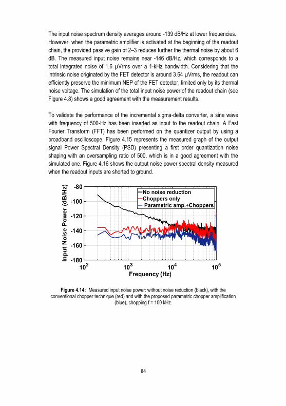
84
The input noise spectrum density averages around -139 dB/Hz at lower frequencies.
However, when the parametric amplifier is activated at the beginning of the readout
chain, the provided passive gain of 2–3 reduces further the thermal noise by about 6
dB. The measured input noise remains near -146 dB/Hz, which corresponds to a
total integrated noise of 1.6 µVrms over a 1-kHz bandwidth. Considering that the
intrinsic noise originated by the FET detector is around 3.64 µVrms, the readout can
efficiently preserve the minimum NEP of the FET detector, limited only by its thermal
noise voltage. The simulation of the total input noise power of the readout chain (see
Figure 4.8) shows a good agreement with the measurement results.
To validate the performance of the incremental sigma-delta converter, a sine wave
with frequency of 500-Hz has been inserted as input to the readout chain. A Fast
Fourier Transform (FFT) has been performed on the quantizer output by using a
broadband oscilloscope. Figure 4.15 represents the measured graph of the output
signal Power Spectral Density (PSD) presenting a first order quantization noise
shaping with an oversampling ratio of 500, which is in a good agreement with the
simulated one. Figure 4.16 shows the output noise power spectral density measured
when the readout inputs are shorted to ground.
Figure 4.14: Measured input noise power: without noise reduction (black), with the conventional chopper technique (red) and with the proposed parametric chopper amplification
(blue), chopping f = 100 kHz.

85
Figure 4.15: Simulated and measured output signal PSD of the incremental sigma-delta
converter tested with an input sinusoidal tone at 500 Hz and sampling rate 1 MHz.
Figure 4.16: Noise PSD measured with shorted input to ground.
The measured SNR is about 65 dB, which is equivalent to be 10.6 effective number
of bits (ENOB), evaluated as [136]:
ENOB = log2 (2Vin,max
VLSB) (4.4)
SNR(dB) = 6 × ENOB + 1.76 (4.5)

86
where Vin,max is the maximum input voltage. To increase the effective number of
bits, the signal should be sampled by the ADC at a rate that is higher than the
system’s required sampling rate (e.g. Nyquist frequency). The sampling rate (fS) of
the incremental converter is set as a trade-off between the integrating capacitance
area, bandwidth of the CT loop filter and the desired resolution, which depends on
the number of clock cycles. Since the FET detected signals are modulated to have a
maximum bandwidth of fsig = 1 kHz, high sampling rate is not necessary.
Therefore, the quantizer is designed to operate with sampling frequency of 1 MHz to
achieve an oversampling ratio (OSR) of 500 for the incremental conversion operation
as given by:
OSR =fs
2 × fsig (4.6)
Figure 4.17: Measured FET voltage responsivity and Noise Equivalent Power (NEP) versus gate bias voltage.
4.5.2 Antenna-Coupled FET Detector Measurements
The performance of a standalone antenna-coupled FET THz detector was evaluated through a lock-in amplifier with sensitivity and time constant of 500 µV and 200 ms, respectively. The FET voltage responsivity was calculated as the measured FET voltage response VFET normalized by the impinging power PFET. By sweeping the
gate bias from the sub-threshold to the strong inversion region, as visible in Figure 4.17, the FET detector achieved a peak responsivity of 318 V/W at a gate bias voltage of about 0.3 V, while it is decreased towards both the strong inversion region, since the Rds was reduced, and thus, the output voltage drop across it

87
decreases, and the sub-threshold, due to the reduction of the cut-off frequency of the FET + lock-in interface, below the source modulation frequency [148], [149].
The FET detector output noise voltage spectrum density was measured around 115
nV/ √Hz, which was equivalent to the thermal noise contribution originated from the
measured FET channel resistance Rds= 800 kΩ at a gate bias voltage of 0.3 V, as
shown in Figure 4.18. Then, NEP can be estimated as the ratio between the
measured thermal noise voltage and the FET responsivity. A minimum NEP of 281
pW/√Hz was obtained at the same gate bias point of 0.3 V.
Figure 4.18: Simulated and measured FET detector noise voltage spectral density versus
frequency.
Figure 4.19: Measured FET Voltage responsivity versus signal frequency.

88
Figure 4.19 shows the frequency sweep analysis for the FET responsivity with an
inset illustrating the THz beam spot sensed by the FET detector. The beam spot was
acquired on an X-Y transverse plane to the optical axis by scanning the pixel chip in
0.4-mm steps using a stepper motor. It is also possible to observe that the FET
detector responsivity is above 200 V/W from 355 – 375 GHz with a peak value of
318 V/W near 365 GHz.
4.6 Readout Responsivity and NEP Measurements
Measurements of responsivity and NEP for the FET THz detector were eventually
acquired through the implemented readout chain, instead of the external lock-in
amplifier. The measurements were performed by modulating the THz source and the
digital modulator at three different frequencies within the range of the FET detector
bandwidth of 1 kHz. Thanks to the digital modulator, the recorded digital response
was the net value of the difference between the two levels of the modulating signal
waveform (with/without the THz signal), such that it could perform the lock-in
function. The voltage response of the FET detector was recorded as 12-bit digital
code through the shift register output per each conversion cycle. The integration time
of the readout chain is related to the modulation frequency of the FET signals (<1
kHz), which was varying in the range of 1 – 10 ms. The measured responsivity as a
function of gate bias voltage is shown in Figure 4.20 at different modulation
frequencies and the same sampling frequency, exhibiting a peak response close a
0.3-V gate bias voltage. Since the readout directly converts the FET response to a
digital output without any representative voltage, except the detector one, we had to
redefine the responsivity. This new definition is obviously not comparable to 𝑅𝑉;
however, the NEP still gives a metric for comparison because it is input-referred. The
responsivity needs to be expressed as the output digital number (DN) per unit of
impinging power (DN/W) instead of (V/W), as given by:
Rdig =DN
PFET (4.7)

89
Figure 4.20: Readout responsivity as a function of FET gate bias voltage.
Figure 4.21: Readout responsivity as a function of signal frequency.
Similarly, Figure 4.21 illustrates the responsivity as a function of signal frequency,
presenting peak values near 365 GHz, similarly to the standalone detector. NEP
curves in Figure 4.22 were measured by calculating the standard deviation of several
acquired digital outputs ∂DN, i.e., the RMS of the output code of each conversion
cycle, divided by the measured responsivity acquired at a signal frequency of 365
GHz. Then, it was divided by the square root of the FET bandwidth (i.e., fmod), as
given by:
NEP =∂DN
Rdig√fmod
(4.8)

90
The minimum NEP value of 376 pW/√Hz was obtained at a gate bias voltage near
0.3 V and a modulation frequency of 130 Hz. The measured NEP was only due to
the thermal noise contribution of the FET detector without being influenced by the
readout noise, since the measured input noise power was significantly below the
FET thermal noise.
However, due to the fact that the dummy FET detector contributes to the total
thermal noise voltage by its channel resistance, the obtained NEP by the readout
chain was approximately √2 times higher than the measured NEP of a single FET
detector. The total NEP of both active and dummy FETs, extracted from the
standalone detector measurements, is visible (dashed line) in Figure 4.22, exhibiting
a good agreement with the readout measurements. It can be noted that the total
NEP (FETs + readout) seems to “cancel” noise at a low gate voltages: this is just an
apparent reduction, due to the fact that the responsivity of the detector alone was
lower in that range due to the larger RC time constant (because of the higher
capacitance for the connection to the instrumentation), which was not present with
the readout chain.
Figure 4.22: NEP as a function of FET gate bias voltage (measured at 365 GHz).
4.7 THz Imaging
As presented in chapter 3, a similar optical experimental setup was used for
performing THz imaging acquisition (see Figure 3.14), with the readout chain
replacing the function of the lock-in amplifier. Metallic and plastic objects concealed
inside a paper envelope were mechanically scanned and captured in transmission

91
mode at 365 GHz and a modulation frequency of 130 Hz. A stepper motor stage was
used to scan the objects in the vertical and horizontal directions by a step size of 0.4
mm. As shown in Figure 4.23, the scanned images clearly resolve the structural
details of the objects such as screws, a SIM card, a nut and a metallic ring. The
scanned area is 20 x 20 mm2 with a total resolution of 50 x 50 pixels.
The background interference pattern appearing in the images was due to the
standing waves generated by multiple reflections inside the paper envelope. The
acquisition time of each image was around 3.5 h, due to the limited speed of the
stepper motors, mainly dominated by the actuator’s speed; however, the effective
acquisition time amounted to just several seconds that compares favourably to an
acquisition with a lock-in amplifier.
Figure 4.23: THz images of different metallic/plastic objects hidden inside a paper envelope
acquired at 365 GHz (source modulation f = 130 Hz) along with the photographs of the objects.
Indeed, usually the lock-in amplifier requires an integration time in the range of 200 –
500 ms in order to achieve similar signal quality, while the proposed readout chain
acquires the data of each pixel during an integration period in the range of 1 – 10
ms, according to the applied modulation frequency. This is regardless of the time
spent by the stepper motors to move between different pixels, showing 2 orders of
magnitude improvement in the acquisition time. The overall performance of the
presented THz pixel structure is summarized in Table 4.1.2 and compared to the
recently-reported state of the art. The proposed THz pixel features: (1) a first order
incremental ADC that is compact in terms of area and power and can be fully
integrated inside the THz pixel, providing simultaneous integration and readout; (2)
suitable for pixels also with smaller antennas (e.g., 800 GHz); (3) it does not require
sources with a high modulation frequency, such that the overall cost of the THz

92
imaging system could be significantly reduced; (4) a direct conversion to the digital
domain, which means robust and easy signal management; (5) low input-referred
noise.
Table 4.1: Performance comparison to the-state-of-the-art.
This Work TTST’2017 [103]
Sensors’16 [132]
JSSC’12 [127]
JSSC’09 [129]
Process 0.15 µm 0.18 µm 0.13 µm 65 nm 0.25 µm
Input Referred
Noise
1.6 µVrms 2.03 µVrms 0.2 µVrms 2.45 µVrms -
Power consumption
80 µW - 320 µW 2.5 µW 5.5 mW
Source Frequency
325 – 375 GHz
860 GHz 270 GHz 856 GHz 650 GHz
Modulation Frequency
10 Hz – 1 kHz
177 Hz 156 kHz 5 kHz 30 kHz
On-chip antenna
Bow-tie antenna
Patch antenna
Bow-tie antenna
Ring antenna
Patch antenna
Pixel size 456 456 µm 2
1330 x 440
µm 2 240 240 µm2 80 80
µm 2 200 150
µm 2
Maximum RV 783
DN/µW 3.3 kV/W 300 kV/W 140 kV/W 80 kV/W
Minimum NEP
376
pW/Hz @ 130 Hz
106
pW/Hz @ 177 kHz
533 pW @ 156 kHz
12 nW @ 500kHz
300
pW/Hz @ 30 kHz

93

94
5
Imaging Arrays and Multispectral Systems
5.1 Motivation
In the chapters 3 and 4, we presented in details the implementation of antenna-
coupled FET detectors and their detection performance was discussed and
compared to the regular FET detectors. Then, the design specifications,
implementation of the in-pixel readout circuit architecture and its characterization
results were discussed. In this chapter we extend a single THz pixel to a multi-pixel
FPA. The multi-pixel imager architecture essentially improves the system
performance by achieving simultaneous signal acquisition of the entire detector array
and therefore, it is expected to bring better detection in different aspects: 1)
increased system sensitivity, since by striking incident radiation on the imager for
longer exposure time with more pixels exposed simultaneously can result in a
reduction of the system bandwidth, and consequently, the noise, 2) the system
resolution is improved with the imager architecture due to its larger number of pixels
in each acquisition for a given exposure time, and lastly, 3) speed (frames per
second) is increased, since a single frame can be obtained faster in the imager
architecture because of parallelization.
In the present work, we also aim to implement multi-spectral detection system with a
special distribution of both visible and THz pixels. The circuits are explained in
details: the pixel structure, comprising the visible pixel and THz pixels used as a
basic building blocks, and their readout circuitries, including also other auxiliary
blocks for addressing and extracting the individual pixels’ values.
5.2 Optimization of The THz Readout Chain
A few modifications have been considered in the THz readout circuit design, based
on the measurements presented in the previous chapter, in order to improve
uniformity for an array implementation. The THz readout circuit is redesigned to be
more robust to the process variation and mismatch effects, in order to reduce pixel-
to-pixel variations; the design modifications are the following:

95
Figure 5.1: Modified Schematic of the Miller Integrator.
In order to increase the flexibility in the integration time, the integrating
capacitors with feedback switches are designed to give four different selectable
bandwidth values (through the switches D0, D1), with the possibility to reset the
integrator output to a predefined value by using the pin VPRE as visible in Figure
5.1. The layout view of the Miller integrator is shown in Figure 5.2. The
integrating capacitors are sized to be C1 = 1 pF, C2 = 0.5 pF and C3 = 0.5 pF.
Figure 5.2: Layout view of the modified Miller Integrator.
The principle of improving the linearity mismatch in the Gm stages is that if
identical nonlinearity is exist at the input and feedback paths they will
compensate each other and the system linearity performance will be improved.
The linearity of the transconductor stages has been improved by reducing the

96
gain. Figure 5.3 shows the DC sweep simulation of the differential input voltage
to the Gm stage versus the achieved transconductance values at different
sourced degenerated resistance values (Schematic is in Figure 4.6).
Figure 5.3: DC sweep simulation of the differential input versus the obtained transconductance value at different source degenerated resistance values.
By increasing the source degenerated resistance from 40 kΩ to 200 kΩ, the
achieved transconductance reduces 24.3 µS to 5.2 µS respectively, resulting
in better linearity. The Gm values in the feed-forward and feedback paths are
scaled to be 20 µS and 3.2 µS, equivalent to degeneration resistors of 50 kΩ
and 312 kΩ, respectively.
The main sources of mismatch in transistors are geometric sizes, process
parameters and errors in drain to source voltages of the mirroring transistors.
Thus, these mainly affect the addition/subtract current from the input and
feedback Gm cells and the Miller integrator. Therefore, in order to provide more
tunability, extra pins are included in the design of the readout circuit such as
VBias_CG, VREF+, VREF-. Moreover, a separate current mirror-based biasing circuit
(see Figure 5.17) is designed to tune the bias current in the CT loop filter (see
Figure 4.6 and Figure 4.7).

97
5.3 Multispectral Imaging Architecture
The proposed multispectral imager architecture is shown in Figure 5.4. It is
composed of a 10 x 10 THz imaging array based on the plasma wave detection,
where each pixel contains an on-chip antenna, a FET detector and an optimized
readout circuit. The visible pixel array is composed of 50 x 50 pixels and it is located
under the antennas, where square slots are formed in the antenna’s ground plane for
illumination. In the bottom part, the readout of visible pixels has been implemented
with a linear array of 50 column correlated double sampling (CDS) circuits. All
column-wise circuits are serialized through the same output amplifier.
Figure 5.4: Multispectral imager architecture.
Figure 5.5 sketches the timing diagram of the imager. It is possible to see that the
THz detector signals are integrated and then readout, row-by-row, during the
integration time of visible pixels, with 1µs of available time to extract the pixel value
by using the parallel-to-serial shift register in the pixel’s readout. Serialization to
output takes place after integration period varying between 1 - 10 ms depending on
the applied modulation frequency of THz source. Visible light integration is
performed during an expected period of 15 - 20 ms, afterwards, 4 ms are allocated
for visible readout at a rate of about 5 MS/s.

98
Figure 5.5: Timing diagram of the multispectral imager.
The imager design is implemented in the same LFoundry 0.15 μm standard CMOS
technology. Figure 5.6 shows the THz pixel layout that includes an on-chip bow-tie
antenna operates at 0.35 THz, a FET detector, and its optimized readout circuit. The
pixel dimensions are 456 μm × 456 μm. The square slots are designed in the
antenna’s ground plane (Metal 1) and located at the same position of the visible
pixels with dimensions of 8 μm x 8 μm, as openings for visible light.
Figure 5.6: Layout of single THz pixel with the readout chain, including also the visible pixel realized under the antenna’s ground plane and in the middle of the readout.

99
The routing of the visible pixels is made by Metal 2 and Metal 3 above the antenna’s
ground plane. Therefore, inside each THz pixel there is a small array of 5 x 5 visible
pixels, with pixel pitch of 91.2 μm. The THz readout chain is compatible with the
antenna size and is placed vertically under the antenna structure. Decoupling
capacitors are utilized at the edges of the analog and digital parts of the readout to
reduce any signal coupling or interference by shorting it to the ground.
5.4 Visible Imaging Array
5.4.1 3T- CMOS Active Pixel Sensor (3T-APS)
The visible pixel is designed as typical three-transistor (3T), photodiode (PD) type
CMOS Active Pixel Sensor (APS). It is composed by a photodiode, a reset transistor
MRST, acts at the beginning of the integration and amplifier transistor MSF, acts as a
source follower that extracts the signal charge and converts it into a voltage [150],
and thus the output voltage follows the PD voltage. The use of a source follower
amplifier improves the image quality and SNR with respect to passive pixel sensors
(PPS). The signal is transferred to a horizontal output line through an access
transistor MSEL. The estimated fill factor (FF) of the pixel is evaluated as:
FF (%) = Light sensitive area
Total pixel area (5.1)
5.4.1.1 Principle of Operation
The operation principle of an APS is described with the timing diagram as visible in
Figure 5.7. Scene integration starts when photodiode is reset when MRST is switched
on. The PD is reset to the voltage value VRST = VDD − Vth, where Vth is the threshold
voltage of transistor MRST. Next, MRST is turned off and the PD is electrically floating.
During the light integration, the photo-generated carriers accumulate in the PD
junction capacitance CPD. The accumulated charge changes the potential in the PD;
the voltage of the PD VPD decreases according to the input light intensity. After an
accumulation time, the select transistor MSEL is switched on and the output signal in
the pixel is read out in a common column line providing also the current for the
biasing. When the readout process is finished, MSEL is switched off and MRST is again
switched on to repeat the above process.

100
Figure 5.7: Pixel schematic of a 3T-APS with the timing diagram.
Typically the pixel voltage range is smaller than the supply voltage. The pixel voltage
range depends on the reset voltage, the threshold voltage of the source follower, and
the overdrive voltage of the load transistor. Increasing the overdrive voltage leads to
increase in the column current and hence lowering the pixel signal range. Therefore,
optimum bias current has to be precisely defined for the image sensor architecture to
achieve the specified speed and noise performance and the pixel signal range during
the design process.
The full-well capacity is the number of charges that can be accumulated in the PD.
The larger the full-well capacity, the higher the dynamic range (DR), which in a linear
pixel is determined as the ratio of the maximum output signal value Vmax to the
minimum detectable signal value Vmin:
DR =Vmax
Vmin [dB] (5.2)
The conversion gain of the pixel is given as the voltage change when one charge
(electron or hole) is accumulated in the PD. The conversion gain is therefore equal to
q/CPD, where q is the electron charge. The full-well capacity increases with larger
PD junction capacitance CPD, while the conversion gain is inversely proportional to
CPD. This indicates a trade-off between the full-well capacity and the conversion
gain.

101
Figure 5.8: Layout of a 3T-APS pixel.
5.4.1.2 Pixel Layout
In the Figure 5.8, the layout of the visible pixel can be seen. It is possible to notice
that the left part is occupied by the photodiode, while the remaining is dedicated for
the layout of the three transistors. Metal 1 and metal 2 are used for internal routing of
the pixel. The photodiode has been implemented in n+/psub diode. The pixel
dimensions are 8 µm x 8 µm, and the fill factor (FF) is estimated to be 73%.
5.4.2 Column-level Correlated Double Sampling Readout
Circuit
Normally, CMOS active pixel sensors suffer from spatial or fixed-pattern noise (FPN)
in the pixel array because of offset and gain non-idealities in the voltage sampling
process and from temporal noise. Temporal noise can be categorized into three
additive components: (1) kTC noise and charge injection interference stemming from
the photodiode reset, (2) photocurrent integration shot noise, and (3) readout noise.

102
Correlated double sampling (CDS) of the pixel voltage is a commonly used technique
to eliminate offset FPN and reset noise in CMOS active pixel sensors[151]. Figure
5.9 shows the CDS circuit that is implemented as a readout circuit in this work. The
operation principle of this CDS circuit is to sample the voltage of the following reset,
such that the final output is the result of subtraction between the integrated value
and the reset, effectively suppressing FPN. In fact, this is not a “true” CDS, as the
reset noise is not subtracted. The implemented CDS includes an operational
transconductance amplifier, a pair of capacitors and some switches.
The current mirror transistor MBBL provides the bias for the source followers inside
every pixel in the same column line. When RSTCDS signal is high, the pixel output is
sampled on the capacitor C1. Next, the pixel must be reset and with the amplifier in
inverting configuration, such that every input signal difference is replicated to the
CDS output. Therefore, if the pixel is reset (RSTPix is high), the pixel reset value is
subtracted from the previously stored value and only the integrated value is available
at the CDS output. The CDS circuit has been simulated with the 3T CMOS APS and
the obtained waveforms are drawn in Figure 5.10 which confirms the timing and
operation principle.
Figure 5.9: Operating principle of column CDS for visible pixel.
Capacitance values of C1 and C2 have been sized to make kTC noise negligible so
to maintain the pixels’ signal to noise ratio until the output of the chip. The purpose of
the switches RSTCDS and its invert in the feedback loop together with the capacitors
is to reset the output voltage to a predefined value, which can be set using the input
pin VREF. In this way, the “zero-level” of the signal can be tuned.

103
Figure 5.10: Transient simulation of the CDS with 3T-APS.
Figure 5.11: Current sweep simulation of visible pixel and CDS circuit.
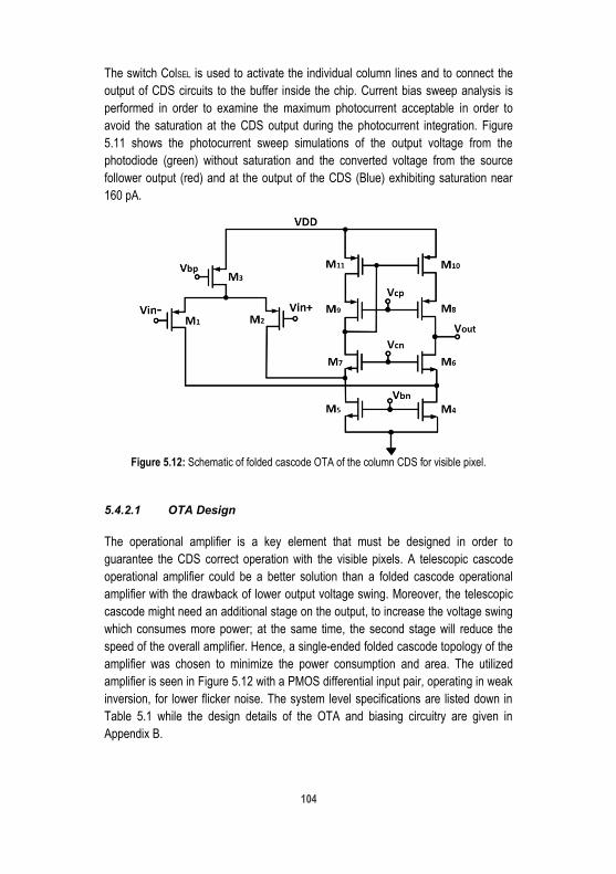
104
The switch ColSEL is used to activate the individual column lines and to connect the
output of CDS circuits to the buffer inside the chip. Current bias sweep analysis is
performed in order to examine the maximum photocurrent acceptable in order to
avoid the saturation at the CDS output during the photocurrent integration. Figure
5.11 shows the photocurrent sweep simulations of the output voltage from the
photodiode (green) without saturation and the converted voltage from the source
follower output (red) and at the output of the CDS (Blue) exhibiting saturation near
160 pA.
Figure 5.12: Schematic of folded cascode OTA of the column CDS for visible pixel.
5.4.2.1 OTA Design
The operational amplifier is a key element that must be designed in order to
guarantee the CDS correct operation with the visible pixels. A telescopic cascode
operational amplifier could be a better solution than a folded cascode operational
amplifier with the drawback of lower output voltage swing. Moreover, the telescopic
cascode might need an additional stage on the output, to increase the voltage swing
which consumes more power; at the same time, the second stage will reduce the
speed of the overall amplifier. Hence, a single-ended folded cascode topology of the
amplifier was chosen to minimize the power consumption and area. The utilized
amplifier is seen in Figure 5.12 with a PMOS differential input pair, operating in weak
inversion, for lower flicker noise. The system level specifications are listed down in
Table 5.1 while the design details of the OTA and biasing circuitry are given in
Appendix B.

105
Table 5.1: System-level specification of the folded cascode operational amplifier.
Technology 0.15 µm
DC Gain 60 dB
Gain Bandwidth (GBW) 30 MHz
Phase Margin (PM) 60º
Load Capacitor 0.5 pF
Input Noise Minimum as possible
Bias Current 10 µA
Supply Voltage 1.8 V
Table 5.2 summarizes the transistor sizes of the implemented single-ended folded-
cascode amplifier with high-swing output, where the total device with is given by m x
W. The switches were implemented with minimum size transistors in a
complementary architecture to reduce the channel charge injection.
Table 5.2: Transistor sizes of the implemented operational amplifier.
Transistor Dimensions (W/L) Multiplier (m)
M1, M2 5 µm / 300 nm 6
M3 5 µm / 2 µm 2
M4, M5 3 µm / 3 µm 2
M6, M7 2.5 µm / 300 nm 4
M8, M9 8 µm / 300 nm 4
M10, M11 5 µm / 2 µm 2
5.4.2.2 Simulation Results
The performance of OTA directly affects the overall performance of the CDS circuit.
Gain and unity gain bandwidth (UGB) of OTA are the key design factors in order to
operate the CDS circuit at high frequency. Beginning with a DC simulation, a total
current consumption of 21.8 μA was obtained, leading to a power consumption of
39.24 μW. The AC simulation curves in Figure 5.13 show a gain of 60.8 dB, a cut-off
frequency of 25.2 kHz, a GBW of 34.92 MHz, and a phase margin of 60.08° for a
load capacitance of 0.5 pF. These main AC parameters are summarized in Table 5.3
for typical conditions and in the four corners (FF, SF, FS, and SS).

106
Figure 5.13: AC simulations of Folded Cascode operational amplifier.
Table 5.3: Amplifier corners simulation results (AC analysis).
TT FF SF FS SS
Gain (dB) 60.8 61.22 60.8 60.26 59.76
PM (deg.) 60.08° 59.92° 60.51° 59.92° 60.51°
GBW (MHz) 34.92 36.37 35.6 33.54 32.76
Figure 5.14: Operational amplifier noise simulation.

107
Since the flicker noise is inversely proportional to gate area, the pMOS differential
pair transistors M1 – M2 were made as large as possible and are designed to
operate in weak inversion with high gm whereas M4 – M5 and M10 – M11 are placed
into strong inversion, which decreases their gm. Several simulations were conducted
to minimize noise, while keeping the stability of the OTA. The noise simulation as a
function of frequency is shown in Figure 5.14 with a total input referred noise of 31.2
μV for a frequency range from 1 Hz to 1 MHz dominated by the input differential pair.
5.4.2.3 Layout of Column-level CDS
Figure 5.15 shows the layout view of the CDS circuit implemented as a column-wise
readout for the visible pixel. An array of 1x 50 CDS circuit was realized at the bottom
of the chip with pitch of 91.2 µm, hence 5 CDS circuits can fit one THz pixel with a
pitch of 456 µm. The layout was realized following the previously described
techniques that minimize gradient induced mismatches.
Figure 5.15: Layout of the column-level CDS readout circuit.

108
Figure 5.16: Bias voltages generation schematic.
5.4.3 Auxiliary Blocks
Some other blocks need to be designed in order to set the operation mode of the
active analog blocks and to control the digital blocks in the chip. In particular these
blocks are utilized to handle the biasing of the circuits and generate the clock and
reset signals and perform signal multiplexing.
5.4.3.1 Bias Generation Circuits
The circuit depicted in Figure 5.16 provides all the needed bias voltages for the
column-level CDS circuit starting from a 10 A input current, as well as the common
line current bias for the visible pixels which is 4 A. The right half part of the circuit
generates the signals for the operational amplifier, as well as the bias voltage for the
preamplifier used in the quantizer block of the THz readout chain.
Figure 5.17: Current mirror schematic for Gm cells and Miller integrator.

109
A separate current mirror circuit is designed for copying the bias current in the Gm
cells and the Miller integrator as visible in Figure 5.17, such that the bias current can
be freely tuned without affecting other generated bias voltages in the chip.
5.4.3.2 Multiplexers
Due to the limited number of pins in the chip, multiplexers are designed to switch
between different readout modes as shown in Figure 5.18. For instance by setting
the THz/VIS input to logic 0, the THz Row/column decoders used to readout the THz
FPA. On the other hand, when logic 1 is set to THz/VIS, the visible pixels can be
scanned and readout using the same EN_Clk and EN_RST pins of the column and
row decoders.
Figure 5.18: Schematic of the multiplexer.
5.4.3.3 Non-Overlapping Clock Generation Circuits
A NOR-flip flop based circuit implements a non-overlapping two-phase clock signal
generator and can be used to derive a two-phase clock signal from a single clock
signal as shown in Figure 5.19. The non-overlapped clock generators are used to
generate the chopper clock signals, and the parametric amplifier control clocks.

110
Figure 5.19: Schematic of the non-overlapped clock generator circuit.
5.4.3.4 Column/Row Decoders
Other blocks include row and column decoders; principally, a row decoder will enable
a particular row and all the pixels will get active in that row, then by using the column
decoder the pixel values are multiplexed one by one to the output buffer. The
decoders are realized as shift-registers by DFF cells from the digital library of the
used CMOS technology as shown in Figure 5.20, where EN_RST and EN_Clk are
the resets and clock signals of the DFFs. A simulation of the waveforms for the row
and column decoders to illustrate the timing is presented in Figure 5.21.
Figure 5.20: Schematic of the implemented row and column decoders.
Figure 5.21: Transient simulation of the implemented row and column decoders.

111
5.4.3.5 Output Buffers
A two-stage Miller OTA is employed as a voltage buffer with unity feedback as
shown in Figure 5.22 (a). In order to maintain the stability of the OTA, a
compensation technique containing a nulling resistor in series with the compensation
capacitor is utilized in the feedback of the second stage to split the low-frequency
poles and achieve the desired phase margin and transient response. The schematic
of the two-stage Miller OTA is depicted in Figure 5.22 (b). The first stage is made up
of a pMOS differential pair (M1-M2) with a current mirror load (M3-M4). The second
stage is realized by common source M7 with current mirror load M6. The required
performance specifications of the Miller OTA are given in Table 5.4. The transistors
dimensions are reported in Table 5.5, where the total device width is given by m x W.
Table 5.4: Design specification of the two-stage Miller OTA.
Technology 0.15 µm
DC Gain 70 dB
Gain Bandwidth (GBW) 30 MHz
Phase Margin (PM) 45º
Load Capacitor 15 pF
Input Noise Minimum as possible
Bias Current 20 µA
Supply Voltage 1.8 V
Table 5.5: Transistors dimensions of the Miller OTA.
Dimensions (W/L) Multiplier (m)
M1,M2 10 µm / 300 nm 10
M3, M4 10 µm / 1 µm 2
M5 10 µm / 1 µm 1
M6 10 µm / 1 µm 4
M7 10 µm / 1 µm 4

112
(a)
(b)
Figure 5.22: Schematic of the output buffer (a), and the implemented Miller OTA (b).
Figure 5.23: The simulated open-loop frequency response of the Miller OTA.
The amplifier was designed to drive a load of 15 pF with a 1.8-V supply voltage.
Figure 5.23 shows the simulated open-loop frequency response of the amplifier.
From the simulation results, the achieved dc gain is around 69 dB, the gain-
bandwidth product is near 28 MHz with a phase margin of 53.08° at the typical
process corner, which are close to the required design specifications. The nulling
resistor of 1.87 kΩŸ load and a compensation capacitance CC = 1.78 pF significantly
improved the stability of the operational amplifier. The obtained corner simulation of
the frequency response of the amplifier is reported in Table 5.6.
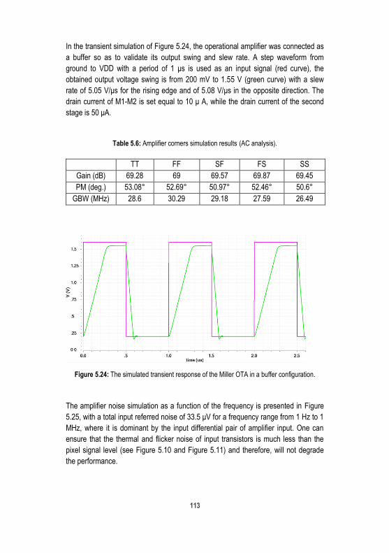
113
In the transient simulation of Figure 5.24, the operational amplifier was connected as
a buffer so as to validate its output swing and slew rate. A step waveform from
ground to VDD with a period of 1 μs is used as an input signal (red curve), the
obtained output voltage swing is from 200 mV to 1.55 V (green curve) with a slew
rate of 5.05 V/μs for the rising edge and of 5.08 V/μs in the opposite direction. The
drain current of M1-M2 is set equal to 10 μ A, while the drain current of the second
stage is 50 μA.
Table 5.6: Amplifier corners simulation results (AC analysis).
TT FF SF FS SS
Gain (dB) 69.28 69 69.57 69.87 69.45
PM (deg.) 53.08° 52.69° 50.97° 52.46° 50.6°
GBW (MHz) 28.6 30.29 29.18 27.59 26.49
Figure 5.24: The simulated transient response of the Miller OTA in a buffer configuration.
The amplifier noise simulation as a function of the frequency is presented in Figure
5.25, with a total input referred noise of 33.5 μV for a frequency range from 1 Hz to 1
MHz, where it is dominant by the input differential pair of amplifier input. One can
ensure that the thermal and flicker noise of input transistors is much less than the
pixel signal level (see Figure 5.10 and Figure 5.11) and therefore, will not degrade
the performance.

114
Figure 5.25: The simulated input noise of the Miller OTA.
The layout of the overall Op-Amp in a buffer configuration is shown in Figure 5.26. The cross-coupled layout technique was used for the first stage to reduce gradient-induced mismatches among the matched transistors. The resistor is laid out in a polysilicon layer. Guard rings are used around the OTA’s components for the supply and ground.
Figure 5.26: Layout of the output buffer using Miller OTA.

115
Figure 5.27: Chip Layout including the core and the padring.
5.4.4 Chip Description
Figure 5.27 shows the layout of the chip including the padring and sealing ring. The
chip is fabricated in the same process technology from LFoundry but with an
updated PDK models for the transistors. The total area occupied by the core is 4.72
mm x 4.68 mm and it contains:
10 x 10 Antenna-coupled FET detectors with in-pixel readout interface.
50 x 50 3T-APS array.
The bottom area is occupied by the visible readout channels (1 x 50)
featuring a CDS circuits.
Biasing and clock generation circuits, output buffers.
Decoupling capacitors are used to fill out the empty space inside the pixels and
around the core array and to filter the supply noise. The chip contains 34 pads
located on the left side including two pins that are double bonded for VSSIO and
VSSCORE pads and VDDIO and VDDCORE pads. While on the top and bottom

116
sides there are 2 pins over bonded on each side. The Chip micrograph is shown in
Figure 5.28 with a zoom showing the pixel structure.
Figure 5.28: Chip micrograph (inset: terahertz pixel structure).

117
The chip testing, at the moment of the thesis writing, is just begun and results are
still not available. The chip is packaged in Ceramic Pin Grid Array (CPGA) with
through-hole 120 gold-plated pins. The CPGA package has a ceramic substrate with
enhanced thermal heat dissipation and a cavity of 11 mm x 11 mm. A testing board
of Figure 5.29 is designed and its layout is drawn in Figure 5.30 . This board will be
mounted on the master board for characterizing the chip.
Figure 5.29: Schematic of the designed PCB testing board.
Figure 5.30: Layout of the designed PCB testing board.

118

119
6
Conclusions and Future Perspectives The main purpose of this work was to develop a room temperature THz detector for
imaging applications by monolithically integrating THz antenna-coupled FET
detector, and readout electronics into a commercial 150 nm CMOS process
technology provided by LFoundry.
Several FET structures were analyzed with respect to the device geometry, aiming to
improve the terahertz detection behavior in the frequencies of 325 – 375 GHz, and
800 GHz – 1 THz. The experimental results obtained from the fabricated chip were
discussed in view of the main performance parameters defined by their NEP and
responsivity. Moreover, the achieved imaging results by scanning were presented.
The measurement results outlined the limitations and improvements suggested for
future implementation and characterization of multi-pixel imaging array.
Initially, design of a single THz pixel was examined with integrated readout circuit,
replacing the lock-in technique and providing digital outputs for the FET detected
signals with improved sensitivity thanks to the low noise performance without
degrading the minimum NEP of the FET detector. A complete design analysis,
simulations, implementation and characterization were presented in chapter 4, where
the experimental results obtained from the circuit blocks compared well to the
simulation ones, validating the readout circuit working principle with the first-order
incremental A/D converter architecture.
The integrated readout noise of 1.6 µVrms over a 1-kHz bandwidth resulted in a
peak-SNR of 65 dB, sufficient for obtaining a good signal quality for THz imaging
applications. The detection behavior of the FET detector with the readout chain has
shown a good sensitivity with a minimum NEP value of 376 pW/√Hz at 365 GHz.
The last part explained the design, simulation, fabrication and characterization of
multispectral imaging system that combines both terahertz and visible frequency
range. Based on the previous measurements of a single THz pixel, several design
aspects are considered to design an optimized version of the readout circuit for
better performance with an improved SNR.

120
The chip contains 10 x 10 FET-based THz imager architecture, that can provide a
simultaneous in-pixel signal integration and noise filtering in order to achieve high
sensitivity at 1-kHz frame rate. Moreover, a vertically integrated 50 x 50 3T – CMOS
APS array is implemented under the THz antennas, with column wise CDS readout
circuits to reduce the FPN. The chip testing just started at the end of this PhD thesis.
The chip characterization results are expected to bring more insights in THz readout
concept, while exhibiting new architecture of the vertically stacked multi-spectral
pixel arrays.
The research presented in this thesis can be extended in several directions. Some of
them are briefly discussed in the following.
Firstly, further investigation should be carried out to keep on enhancing the FET
detector sensitivity. For instance, a combined FET detector structures that take the
advantages of both Extended Source FET and Trapezoidal gate FETs can be
realized. Thus these new FETs are expected to have lower intrinsic thermal noise,
and at the same time, achieve higher self-mixing efficiency. Moreover, the FET
detector performance should be analyzed with the trend of downscaling of CMOS
technology.
Secondly, the implementation of high frequency focal plane arrays is still an object
that can bring much higher resolution and lower cost of THz imaging applications. In
this work pixel structures operating in the frequency range 0.85 – 1 THz are
designed and characterized. Using readout circuits connected to these high
frequency FET-based pixels is likely to bring a better performance, with an improved
SNR. However, still high intensity THz power sources are needed to generate THz
signals with sufficient impinging power.
Lastly, still additional studies should be carried out to analyze the THz detection
performance of the Graphene-based FETs (GFETs) detectors. Graphene-based
FETs is expected to have excellent optical and electronic properties over standard
FETs, since it has higher carrier mobility and only requires planar processing
technologies similar to the ones already employed in the existing CMOS technology.
Beside FET-based THz imagers, the existing microbolometer imagers (e.g. the
MICROXCAM-384I-THZ by INO, Canada) and large integrated pyroelectric THz
imaging arrays (e.g. the Pyrocam IIIHR by Ophir Inc.) are still leading the market
trends thanks to their high performance however if heterodyning detection is taken
into account, then the advantage of FET imagers is very clear since thermal
detectors cannot work in heterodyne mode.

121

122
Appendix A: System-level Simulation: Matlab Simulink
Figure A-1: Matlab Simulink model of Incremental Sigma Delta ADC
Figure A-2 shows the transient simulation results of Incremental Sigma Delta ADC
modelled by Matlab Simulink at the following conditions: Signal frequency = 1 kHz,
sampling frequency = 1 MHz, OSR = 500, and chopping frequency = 100 kHz.
Figure A-2: Transient simulation results of Incremental Sigma Delta ADC modelled by Matlab
Simulink

123
Figure A-3 shows the signal power spectral density (PSD) of Incremental Sigma
Delta ADC obtained by executing a fast Fourier transform (FFT) on the transient
response of the quantizer output with a Hann window function. The output spectrum
of the incremental ADC has been analyzed while the chopper technique is in active
mode. The incremental ADC achieves 68-dB peak signal-to-noise ratio (SNR)
equivalent to 10.7 bits effective resolution.
Figure A-3: signal power spectral density (PSD) results of Incremental Sigma Delta ADC
modelled by Matlab Simulink.

124
Appendix B: Folded Cascode OTA Design Analysis
This section presents the analysis of a single-ended folded-cascode OTA that is
utilized in the CDS circuit whose circuit diagram is presented in Figure B-1. A PMOS
differential input pair (M1 and M2), operating in weak inversion, is used for lower
flicker noise. Transistors M6 - M8 are cascode transistors to increase the output
resistance. Transistors M4 and M5 have a larger W/L with respect to the other
mirrors, but still smaller with respect to the differential pair.
Figure B-1: Schematic of folded cascode OTA of the column CDS for visible pixel.
To proceed with the OTA design, the main parameters of the chosen technology
were verified through a DC simulation of a NMOS and a PMOS and using equations
Eq. B − 1 and Eq. B − 2, where ID is the drain current, rDS is the drain to source
resistance, λ is the channel-length modulation.
ID =μCox
2
W
L(VGS − VTH)2 (B − 1)
rDS =L
λID (B − 2)
125
The OTA performance parameters are determined as follows: the small signal voltage gain of a folded cascode is given by:
Av = Gm ∗ Rout (B − 3)
Where Gm represents the equivalent transconductance of the OTA and Rout
represents its output impedance. Both are defined as:
Gm =ID
Vin ≈ gm1 (B − 4)
Rout = [gm8 rDS8rDS10]⧸⧸[gm6rDS6(rDS4//rDS1)] (B − 5)
Therefore, the voltage gain Av can be obtained as:
Av = gm1 ∗ [gm8 rDS8rDS10]⧸⧸[gm6rDS6(rDS4//rDS1)] (B − 6)
The dominant pole occurs at the output node due to the high impedance Rout seen
looking through that node. The location of dominant pole is given by:
ωp1 = ω3dB =1
RoutCL (B − 7)
Where CL represents the total capacitance present at the output node and is given
by: CL = Cload + Cgd8 + Cdb8 + Cgd6 + Cdb6 (B − 8)
The unity gain bandwidth of the OTA is given by:
fUGB = Av ∗ ω3db =gm1
CL (B − 9)
For a given capacitive load, the unity gain bandwidth can be increased by increasing gm1 of the input differential pair.
The input common mode range (ICMR) of the OTA is defined as the voltage range
that can be applied to the input transistors without driving any transistor into triode
region. The input common voltage Vin,CM that can place M3 at the edge of
saturation is defined as:
Vin,CM max = VDD − Vov3 − |VGS1| (B − 10)

126
where Vov3 is the overdrive voltage of M3 and is given by:
|Vov3| = |VSG3 − |Vth3| | (B − 11)
On the other hand Vin,CM can be low enough to place M3 and M4 at the edge of
saturation region.
Vin,CM min = Vov4 − |Vth1| (B − 12)
where 𝑉𝑜𝑣4 is the overdrive voltage of M4, therefore, the input common mode range
is given as:
Vov4 − |Vth1| ≤ Vin,CM ≤ VDD − Vov3 − |VGS1| (B − 13)
A wide-swing current mirror is realized through the connection between the gate of
M11 and the drain of M9. The amplifier maximum output voltage is given by:
Vout,max = VDD − |Vov11| − |VGS9| + |VTH8| (B − 14)
This obtained output voltage is one threshold voltage higher than the one using regular output mirrors, the minimum output voltage is given by:
Vout,min = Vov4 + Vov6 (B − 15)
Concerning the OTA bias voltages, Vbp and Vbnare generated with current mirrors
and an external current source, while Vcn and Vcp are obtained with diode-
connected transistors according to their estimated minimum values (to be increased
by a safety margin) given by:
Vcn = Vov4 + VGS6 (B − 16)
Vcp = VDD − |Vov11| − |VGS9| (B − 17)

127

128
Bibliography
[1] P. H. Siegel, “Terahertz technology,” IEEE Trans. Microw. Theory
Tech., vol. 50, no. 3, pp. 910–928, 2002.
[2] C. Sirtori, “Applied physics: Bridge for the terahertz gap,” Nature,
vol. 417, no. 6885, pp. 132–133, May 2002.
[3] M. C. Kemp, “Millimetre wave and terahertz technology for
detection of concealed threats - a review,” undefined, 2007.
[4] D. D. Ferris, Jr. and N. C. Currie, “<title>Overview of current
technology in MMW radiometric sensors for law enforcement
applications</title>,” 2000, vol. 4032, pp. 61–71.
[5] J. F. Federici et al., “THz imaging and sensing for security
applications—explosives, weapons and drugs,” Semicond. Sci.
Technol., vol. 20, no. 7, pp. S266–S280, Jul. 2005.
[6] M. Shur, “Terahertz electronics for sensing applications BT -
Sensors, 2011 IEEE,” pp. 40–43, 2011.
[7] A. Y. Pawar, D. D. Sonawane, K. B. Erande, and D. V. Derle,
“Terahertz technology and its applications,” Drug Invent. Today,
vol. 5, no. 2, pp. 157–163, Jun. 2013.
[8] X. Yang et al., “Biomedical Applications of Terahertz Spectroscopy
and Imaging.,” Trends Biotechnol., vol. 34, no. 10, pp. 810–824,
Oct. 2016.
[9] A. G. Davies, A. D. Burnett, W. Fan, E. H. Linfield, and J. E.
Cunningham, “Terahertz spectroscopy of explosives and drugs,”
Mater. Today, vol. 11, no. 3, pp. 18–26, Mar. 2008.
[10] T. Lu, H. Yuan, Z. Zhang, T. Wu, C. Zhang, and Y. Zhao,
“Experimental 210GHz terahertz nondestructive testing for
aerospace composite materials,” in 2016 13th International
Bhurban Conference on Applied Sciences and Technology
(IBCAST), 2016, pp. 714–717.
[11] J. C. Dickinson et al., “Terahertz imaging of subjects with
concealed weapons,” 2006, p. 62120Q.
[12] E. Bründermann, H.-W. Hübers, and M. F. Kimmitt, Terahertz

129
Techniques, vol. 151. Berlin, Heidelberg: Springer Berlin
Heidelberg, 2012.
[13] T. Nagatsuma, “Generating millimeter and terahertz waves by
photonics for communications and sensing,” IEEE MTT-S Int.
Microw. Symp. Dig., no. June 2009, pp. 1–3, 2013.
[14] K. Moon et al., “Generation and Detection of Terahertz Waves
Using Low-Temperature-Grown GaAs with an Annealing Process,”
ETRI J., vol. 36, no. 1, pp. 159–162, Feb. 2014.
[15] N. Kim et al., “Tunable continuous-wave terahertz
generation/detection with compact 155 μm detuned dual-mode
laser diode and InGaAs based photomixer,” Opt. Express, vol. 19,
no. 16, p. 15397, Aug. 2011.
[16] M. S. Apu and N. Kaabouch, “Characteristics of the Terahertz
sources suitable for biomedical applications,” in 2012 IEEE
International Conference on Electro/Information Technology, 2012,
pp. 1–5.
[17] E. L. Jacobs et al., “Concealed weapon identification using
terahertz imaging sensors,” 2006, p. 62120J.
[18] M. C. Kemp, A. Glauser, and C. Baker, “Recent developments in
people screening using terahertz technology: seeing the world
through terahertz eyes,” 2006, p. 62120T.
[19] J. F. Federici, D. Gary, R. Barat, and D. Zimdars, “<title>THz
standoff detection and imaging of explosives and weapons (Invited
Paper)</title>,” 2005, vol. 5781, pp. 75–84.
[20] Y. Yang, “Atmospheric Effects on Free-Space THz,” J. Lasers, Opt.
Photonics, vol. 01, no. 02, pp. 1–2, Jul. 2014.
[21] M. Perenzoni and D. J. Paul, Physics and applications of terahertz
radiation. .
[22] E. Bründermann, H.-W. Hübers, and M. F. Kimmitt, “Sources,”
2012, pp. 103–168.
[23] E. Bründermann, H.-W. Hübers, and M. F. Kimmitt, “Detectors,”
2012, pp. 169–245.
[24] “Terahertz security applications | TeraSense.” [Online]. Available:
http://terasense.com/applications/security/. [Accessed: 04-Aug-
2018].
[25] M. C. Kemp, P. F. Taday, B. E. Cole, J. A. Cluff, A. J. Fitzgerald,
130
and W. R. Tribe, “Security applications of terahertz technology,”
2003, p. 44.
[26] “Terahertz-based imaging in medical diagnostics | TeraSense.”
[Online]. Available: http://terasense.com/applications/medical-
diagnostics/. [Accessed: 04-Aug-2018].
[27] J.-H. Son, “Biomedical science and technology using terahertz
waves,” in 2015 11th Conference on Lasers and Electro-Optics
Pacific Rim (CLEO-PR), 2015, pp. 1–1.
[28] K.-E. Peiponen, A. Zeitler, and M. Kuwata-Gonokami, Eds.,
Terahertz Spectroscopy and Imaging, vol. 171. Berlin, Heidelberg:
Springer Berlin Heidelberg, 2013.
[29] P. U. Jepsen, D. G. Cooke, and M. Koch, “Terahertz spectroscopy
and imaging - Modern techniques and applications,” Laser Photon.
Rev., vol. 5, no. 1, pp. 124–166, Jan. 2011.
[30] N. N. Almoayed and M. N. Afsar, “High resolution fourier transform
spectroscopy of environmentally hazardous gases at millimeter and
submillimeter wavelengths,” in 2007 Joint 32nd International
Conference on Infrared and Millimeter Waves and the 15th
International Conference on Terahertz Electronics, 2007, pp. 178–
179.
[31] J.-N. Liu, M. V. Schulmerich, R. Bhargava, and B. T. Cunningham,
“Narrowband Guided Fano Resonators for Mid-Infrared
Spectroscopy and Imaging,” in CLEO: 2014, 2014, p. ATu3P.5.
[32] M. Naftaly and R. E. Miles, “Terahertz time-domain spectroscopy: A
new tool for the study of glasses in the far infrared,” J. Non. Cryst.
Solids, vol. 351, no. 40–42, pp. 3341–3346, Oct. 2005.
[33] D. Saeedkia and S. Safavi-Naeini, “Terahertz Photonics:
Optoelectronic Techniques for Generation and Detection of
Terahertz Waves,” J. Light. Technol., vol. 26, no. 15, pp. 2409–
2423, Aug. 2008.
[34] K. Kawase, T. Shibuya, S. Hayashi, and K. Suizu, “THz imaging
techniques for nondestructive inspections,” Comptes Rendus
Phys., vol. 11, no. 7–8, pp. 510–518, Aug. 2010.
[35] S. Wietzke et al., “Industrial applications of THz systems,” 2009,
vol. 7385, p. 738506.
[36] S. U. Hwu, K. B. deSilva, and C. T. Jih, “Terahertz (THz) wireless
131
systems for space applications,” in 2013 IEEE Sensors Applications
Symposium Proceedings, 2013, pp. 171–175.
[37] J. Federici and L. Moeller, “Review of terahertz and subterahertz
wireless communications,” J. Appl. Phys., vol. 107, no. 11, p.
111101, Jun. 2010.
[38] K. R. Jha and G. Singh, “Development in the Terahertz
Communication System,” in Terahertz Planar Antennas for Next
Generation Communication, Cham: Springer International
Publishing, 2014, pp. 185–203.
[39] R. Piesiewicz et al., “Short-range ultra-broadband terahertz
communications: Concepts and perspectives,” IEEE Antennas
Propag. Mag., vol. 49, no. 6, pp. 24–39, 2007.
[40] A. G. Davies, E. H. Linfield, and M. B. Johnston, “The development
of terahertz sources and their applications,” Phys. Med. Biol., vol.
47, no. 21, pp. 3679–3689, Nov. 2002.
[41] K. R. Jha and G. Singh, “Terahertz Sources and Antennas,” in
Terahertz Planar Antennas for Next Generation Communication,
Cham: Springer International Publishing, 2014, pp. 1–22.
[42] S. Krishnagopal and V. Kumar, “Free-electron lasers,” Radiat.
Phys. Chem., vol. 70, no. 4–5, pp. 559–569, Jul. 2004.
[43] E. Tuncel et al., “Free-electron laser studies of direct and indirect
two-photon absorption in germanium,” Phys. Rev. Lett., vol. 70, no.
26, pp. 4146–4149, Jun. 1993.
[44] G. S. Edwards et al., “Free-electron lasers: reliability, performance,
and beam delivery,” IEEE J. Sel. Top. Quantum Electron., vol. 2,
no. 4, pp. 810–817, 1996.
[45] Y. Park et al., “Design and development of 90 GHz backward-wave
oscillator with staggered double-vane slow-wave structure,” in 2016
IEEE International Vacuum Electronics Conference (IVEC), 2016,
pp. 1–2.
[46] R. L. Ives et al., “Design and Test of a Submillimeter-Wave
Backward Wave Oscillator,” in 2005 Joint 30th International
Conference on Infrared and Millimeter Waves and 13th
International Conference on Terahertz Electronics, vol. 1, pp. 93–
94.
[47] L. Qing-Lun, W. Zi-Cheng, and L. Pu-Kun, “Simulation of the

132
backward wave oscillator as a THz radiation source,” in 2012
International Conference on Microwave and Millimeter Wave
Technology (ICMMT), 2012, pp. 1–2.
[48] J. M. Neilson, R. L. Ives, M. Caplan, M. Mizuhara, D. Marsden, and
C. Kory, “High efficiency, terahertz, backward wave oscillators,” in
IEEE Conference Record - Abstracts. 2002 IEEE International
Conference on Plasma Science (Cat. No.02CH37340), p. 171.
[49] N. Orihashi, S. Suzuki, and M. Asada, “One THz harmonic
oscillation of resonant tunneling diodes,” Appl. Phys. Lett., vol. 87,
no. 23, p. 233501, Dec. 2005.
[50] E. R. Brown and C. D. Parker, “Resonant Tunnel Diodes as
Submillimetre-Wave Sources,” Philos. Trans. R. Soc. A Math. Phys.
Eng. Sci., vol. 354, no. 1717, pp. 2365–2381, Oct. 1996.
[51] F. Friederich et al., “THz active imaging systems with real-time
capabilities,” IEEE Trans. Terahertz Sci. Technol., vol. 1, no. 1, pp.
183–200, 2011.
[52] D. Pardo, J. Grajal, C. G. Perez-Moreno, and S. Perez, “An
Assessment of Available Models for the Design of Schottky-Based
Multipliers Up to THz Frequencies,” IEEE Trans. Terahertz Sci.
Technol., vol. 4, no. 2, pp. 277–287, Mar. 2014.
[53] A. Maestrini et al., “Schottky diode-based terahertz frequency
multipliers and mixers,” Comptes Rendus Phys., vol. 11, no. 7–8,
pp. 480–495, Aug. 2010.
[54] Y. Zhang, W. Zhong, T. Ren, Y. Chen, B. Yan, and R. Xu, “A 220
GHz frequency tripler based on 3D electromagnetic model of the
schottky diode and the field-circuit co-simulation method,” Microw.
Opt. Technol. Lett., vol. 58, no. 7, pp. 1647–1651, Jul. 2016.
[55] D. Stanze, A. Deninger, A. Roggenbuck, S. Schindler, M. Schlak,
and B. Sartorius, “Compact cw Terahertz Spectrometer Pumped at
1.5 μm Wavelength,” J. Infrared, Millimeter, Terahertz Waves, vol.
32, no. 2, pp. 225–232, Feb. 2011.
[56] T. Y. Chang and T. J. Bridges, “Laser action at 452, 496, and 541
μm in optically pumped CH3F,” Opt. Commun., vol. 1, no. 9, pp.
423–426, Apr. 1970.
[57] Y. Yao, Z. Liu, A. J. Hoffman, K. J. Franz, and C. F. Gmachl,
“Voltage Tunability of Quantum Cascade Lasers,” IEEE J. Quantum

133
Electron., vol. 45, no. 6, pp. 730–736, Jun. 2009.
[58] C. Walther, G. Scalari, J. Faist, H. Beere, and D. Ritchie, “Low
frequency terahertz quantum cascade laser operating from
1.6to1.8THz,” Appl. Phys. Lett., vol. 89, no. 23, p. 231121, Dec.
2006.
[59] J. Faist, F. Capasso, C. Sirtori, D. L. Sivco, A. L. Hutchinson, and
A. Y. Cho, “Laser action by tuning the oscillator strength,” Nature,
vol. 387, no. 6635, pp. 777–782, Jun. 1997.
[60] S. Preu, G. H. Döhler, S. Malzer, L. J. Wang, and A. C. Gossard,
“Tunable, continuous-wave Terahertz photomixer sources and
applications,” J. Appl. Phys., vol. 109, no. 6, p. 061301, Mar. 2011.
[61] S. Matsuura et al., “A traveling-wave THz photomixer based on
angle-tuned phase matching,” Appl. Phys. Lett., vol. 74, no. 19, pp.
2872–2874, May 1999.
[62] E. R. Brown, “THz Generation by Photomixing in Ultrafast
Photoconductors,” Int. J. High Speed Electron. Syst., vol. 13, no.
02, pp. 497–545, Jun. 2003.
[63] R. Mendis, C. Sydlo, J. Sigmund, M. Feiginov, P. Meissner, and H.
L. Hartnagel, “Tunable CW-THz system with a log-periodic
photoconductive emitter,” 2003 Int. Semicond. Device Res. Symp.
ISDRS 2003 - Proc., vol. 48, pp. 318–319, 2003.
[64] P. Focardi, W. R. McGrath, and A. Neto, “Design guidelines for
terahertz mixers and detectors,” IEEE Trans. Microw. Theory Tech.,
vol. 53, no. 5, pp. 1653–1660, 2005.
[65] T. Otsuji, “Trends in the Research of Modern Terahertz Detectors:
Plasmon Detectors,” IEEE Trans. Terahertz Sci. Technol., vol. 5,
no. 6, pp. 1110–1120, 2015.
[66] V. Giliberti et al., “Heterodyne and subharmonic mixing at 0.6 THz
in an AlGaAs/InGaAs/AlGaAs heterostructure field effect transistor,”
Appl. Phys. Lett., vol. 103, no. 9, p. 093505, Aug. 2013.
[67] D. Glaab, S. Boppel, A. Lisauskas, U. Pfeiffer, E. Öjefors, and H. G.
Roskos, “Terahertz heterodyne detection with silicon field-effect
transistors,” Appl. Phys. Lett., vol. 96, no. 4, p. 042106, Jan. 2010.
[68] J. C. Pearson et al., “Demonstration of a room temperature 2.48–
2.75 THz coherent spectroscopy source,” Rev. Sci. Instrum., vol.
82, no. 9, p. 093105, Sep. 2011.

134
[69] M. J. E. Golay, “A Pneumatic Infra‐Red Detector,” Rev. Sci.
Instrum., vol. 18, no. 5, pp. 357–362, May 1947.
[70] G. M. J. E, Radiation detecting device. 1951.
[71] Yingxin Wang, Ziran Zhao, Zhiqiang Chen, and Linghui Wang,
“Characterization of Golay detector for the absolute power
measurement of terahertz radiation,” in 2012 37th International
Conference on Infrared, Millimeter, and Terahertz Waves, 2012, pp.
1–2.
[72] D. R. Denison, M. E. Knotts, M. E. McConney, and V. V. Tsukruk,
“Experimental characterization of mm-wave detection by a micro-
array of Golay cells,” 2009, p. 73090J.
[73] D. R. Denison, M. E. Knotts, H. T. Hayden, S. L. Young, and V. V.
Tsukruk, “Influence of micro-Golay cell cavity diameter on
millimeter-wave detection sensitivity,” in 2011 International
Conference on Infrared, Millimeter, and Terahertz Waves, 2011, pp.
1–2.
[74] D. Klocke, A. Schmitz, H. Soltner, H. Bousack, and H. Schmitz,
“Infrared receptors in pyrophilous (‘fire loving’) insects as model for
new un-cooled infrared sensors,” Beilstein J. Nanotechnol., vol. 2,
pp. 186–197, Mar. 2011.
[75] L. O. T. Fernandes et al., “Photometry of THz radiation using Golay
cell detector,” in 2011 XXXth URSI General Assembly and
Scientific Symposium, 2011, pp. 1–4.
[76] E. R. Brown, H. Bagherzadeh, and W.-D. Zhang, “Sub-THz power
measurements with ambient pyroelectric detectors,” in 2016 41st
International Conference on Infrared, Millimeter, and Terahertz
waves (IRMMW-THz), 2016, pp. 1–2.
[77] A. F. E. Mejia, J. A. Bava, and J. O. Tocho, “Image detection with
pyroelectric sensors,” in 2017 XVII Workshop on Information
Processing and Control (RPIC), 2017, pp. 1–4.
[78] P. K. Day, H. G. LeDuc, B. A. Mazin, A. Vayonakis, and J.
Zmuidzinas, “A broadband superconducting detector suitable for
use in large arrays,” Nature, vol. 425, no. 6960, pp. 817–821, Oct.
2003.
[79] Z. Li, Q. Shi, W. Lv, J. Li, and S. Shi, “Characterization of an 8×8 Al
microwave kinetic inductance detector array,” in 2018 IEEE MTT-S

135
International Wireless Symposium (IWS), 2018, pp. 1–3.
[80] C. Dietlein, J. D. Chisum, M. D. Ramírez, A. Luukanen, E. N.
Grossman, and Z. Popović, “Integrated microbolometer antenna
characterization from 95-650 GHz,” IEEE MTT-S Int. Microw.
Symp. Dig., pp. 1165–1168, 2007.
[81] P. L. Richards, “Bolometers for infrared and millimeter waves,” J.
Appl. Phys., vol. 76, no. 1, pp. 1–24, Jul. 1994.
[82] Y. Jiang, B. Jin, W. Xu, L. Kang, J. Chen, and P. Wu, “Terahertz
detectors based on superconducting hot electron bolometers,” Sci.
China Inf. Sci., vol. 55, no. 1, pp. 64–71, Jan. 2012.
[83] S. Cherednichenko, A. Hammar, S. Bevilacqua, V. Drakinskiy, J.
Stake, and A. Kalabukhov, “A Room Temperature Bolometer for
Terahertz Coherent and Incoherent Detection,” IEEE Trans.
Terahertz Sci. Technol., vol. 1, no. 2, pp. 395–402, Nov. 2011.
[84] B. Hu, P. Li, A. Ruan, and D. Lin, “Design and verification of 160 ×
120 bolometer ROIC,” in 2011 International Conference on
Computational Problem-Solving (ICCP), 2011, pp. 275–278.
[85] M. Perenzoni, F. Borghetti, and L. Gonzo, “A column readout
channel for infrared and terahertz bolometers with direct analog to
digital conversion,” in Proceedings of 2010 IEEE International
Symposium on Circuits and Systems, 2010, pp. 1288–1291.
[86] S. Hwang, A. Shin, H. Shin, and M. Sung, “A CMOS Readout IC
Design for Uncooled Infrared Bolometer Image Sensor Application,”
in 2006 IEEE International Symposium on Industrial Electronics,
2006, pp. 2788–2791.
[87] R. Han et al., “Active terahertz imaging using schottky diodes in
CMOS: Array and 860-ghz pixel,” IEEE J. Solid-State Circuits,
2013.
[88] O. Doussin, D. Bajon, S. Wane, P. Magnan, and T. Parra,
“Integrated Schottky diodes for sub-millimeter and THz passive
imaging: Influence of detector arrays topology,” in 2013 IEEE 13th
Topical Meeting on Silicon Monolithic Integrated Circuits in RF
Systems, 2013, pp. 33–35.
[89] O. Doussin, D. Bajon, S. Wane, P. Magnan, and T. Parra,
“Integrated Schottky Diodes for sub-millimeter and THz passive
imaging: Influence of detector arrays topology,” in 2013 IEEE Radio

136
and Wireless Symposium, 2013, pp. 52–54.
[90] D. Y. Kim, S. Park, R. Han, and K. O. Kenneth, “820-GHz Imaging
Array Using Diode-Connected NMOS Transistors in 130-nm
CMOS,” Symp. VLSI Circuits, 2013.
[91] C. Sydlo, O. Cojocari, D. Schçnherr, T. Goebel, P. Meissner, and
H. L. Hartnagel, “Fast THz detectors based on InGaAs Schottky
Diodes,” Frequenz, vol. 62, no. 5–6, pp. 107–110, Jun. 2008.
[92] R. Han et al., “280GHz and 860GHz image sensors using Schottky-
barrier diodes in 0.13μm digital CMOS,” in 2012 IEEE International
Solid-State Circuits Conference, 2012, pp. 254–256.
[93] W. Knap and M. I. Dyakonov, “Field effect transistors for terahertz
applications,” in Handbook of Terahertz Technology for Imaging,
Sensing and Communications, Elsevier, 2013, pp. 121–155.
[94] P. Földesy, “Characterization of silicon field effect transistor sub-
THz detectors for imaging systems,” 2012.
[95] A. Lisauskas et al., “Terahertz responsivity and low-frequency noise
in biased silicon field-effect transistors,” Appl. Phys. Lett., vol. 102,
no. 15, p. 153505, Apr. 2013.
[96] V. Y. Kachorovskii, S. L. Rumyantsev, W. Knap, and M. Shur,
“Performance limits for field effect transistors as terahertz
detectors,” Appl. Phys. Lett., vol. 102, no. 22, p. 223505, Jun. 2013.
[97] A. Lisauskas, S. Boppel, V. Krozer, and H. G. Roskos, “Silicon
CMOS-based THz detection,” Proc. IEEE Sensors, pp. 55–58,
2011.
[98] Y. M. Meziani et al., “Terahertz imaging using strained-Si
MODFETs as sensors,” Solid. State. Electron., vol. 83, pp. 113–
117, 2013.
[99] W. Knap et al., “Field effect transistors for terahertz detection:
Physics and first imaging applications,” J. Infrared, Millimeter,
Terahertz Waves, vol. 30, no. 12, pp. 1319–1337, 2009.
[100] M. Dyakonov and M. Shur, “Shallow water analogy for a ballistic
field effect transistor: New mechanism of plasma wave generation
by dc current,” Phys. Rev. Lett., vol. 71, no. 15, pp. 2465–2468,
Oct. 1993.
[101] A. Golenkov and F. Sizov, “Terahertz FET direct detection rectifying
detectors,” pp. 8–11, 2015.
137
[102] S. Chai, S. Lim, and S. Hong, “THz detector with an antenna
coupled stacked CMOS plasma-wave FET,” IEEE Microw. Wirel.
Components Lett., vol. 24, no. 12, pp. 869–871, 2014.
[103] Z. Y. Liu, L. Y. Liu, J. Yang, and N. J. Wu, “A CMOS Fully
Integrated 860-GHz Terahertz Sensor,” IEEE Trans. Terahertz Sci.
Technol., vol. 7, no. 4, pp. 455–465, 2017.
[104] S. Boppel, A. Lisauskas, M. Saphar, V. Krozer, and H. G. Roskos,
“CMOS detector arrays for coherent THz imaging: From point-to-
point towards plane-to-plane imaging configurations,” 2012 19th Int.
Conf. Microwaves, Radar Wirel. Commun. MIKON 2012, vol. 1, pp.
112–115, 2012.
[105] D. M. Yermolayev et al., “Terahertz detection in a slit-grating-gate
field-effect-transistor structure.”
[106] A. A. Generalov, M. A. Andersson, X. Yang, and J. Stake,
“Optimization of THz graphene FET detector integrated with a
bowtie antenna,” 2016 10th Eur. Conf. Antennas Propagation,
EuCAP 2016, pp. 3–5, 2016.
[107] L. Vicarelli et al., “Graphene field-effect transistors as room-
temperature terahertz detectors,” Nat. Mater., vol. 11, no. 10, pp.
865–871, Oct. 2012.
[108] X. Yang, A. Vorobiev, A. Generalov, M. A. Andersson, and J.
Stake, “A flexible graphene terahertz detector,” Appl. Phys. Lett.,
vol. 111, no. 2, p. 021102, Jul. 2017.
[109] P. W. Kruse and Society of Photo-optical Instrumentation
Engineers., Uncooled thermal imaging : arrays, systems, and
applications. SPIE, 2001.
[110] J. Grzyb, H. Sherry, A. Cathelin, A. Kaiser, and U. R. Pfeiffer, “On
the co-design between on-chip antennas and THz MOSFET direct
detectors in CMOS technology,” Int. Conf. Infrared, Millimeter,
Terahertz Waves, IRMMW-THz, pp. 5–7, 2012.
[111] S. Domingues et al., “analysis of CMOS test structures for THz
imaging,” Ieee, pp. 6–7, 2013.
[112] S. Boppel et al., “CMOS integrated antenna-coupled field-effect-
transistors for the detection of 0.2 to 4.3 THz,” 2012 IEEE 12th Top.
Meet. Silicon Monolith. Integr. Circuits RF Syst. SiRF 2012 - Dig.
Pap., pp. 77–80, 2012.

138
[113] S. Domingues et al., “Analysis of CMOS 0.13µm test structures for
0.6 to 1.5 THz imaging,” in 2013 38th International Conference on
Infrared, Millimeter, and Terahertz Waves (IRMMW-THz), 2013, pp.
1–2.
[114] N. Monnier et al., “Study of CMOS THz pixels using different
antenna geometries on metamaterial structures and in-pixel high-
performances signal processing,” Int. Conf. Infrared, Millimeter,
Terahertz Waves, IRMMW-THz, pp. 3–4, 2017.
[115] S. Boppel et al., “CMOS integrated antenna-coupled field-effect
transistors for the detection of radiation from 0.2 to 4.3 THz,” IEEE
Trans. Microw. Theory Tech., vol. 60, no. 12, pp. 3834–3843, 2012.
[116] S. Domingues, D. Perenzoni, M. Perenzoni, and D. Stoppa, “CMOS
Integrated Lock-in Readout Circuit for FET Terahertz Detectors,” J.
Infrared, Millimeter, Terahertz Waves, vol. 38, no. 6, pp. 679–688,
2017.
[117] M. Ali and M. Perenzoni, “A Readout Channel Optimized for
Minimum NEP of a FET-Based THz Pixel,” vol. 1, 2018.
[118] M. Khatib and M. Perenzoni, “Pixel-level continuous-time
incremental sigma-delta A/D converter for THz sensors,” 2016, p.
98990E.
[119] S. Domingues, D. Perenzoni, M. Perenzoni, and D. Stoppa,
“Design and characterization of a readout circuit for FET-based
THz imaging,” 2014, p. 914105.
[120] U. R. Pfeiffer et al., “A CMOS focal-plane array for terahertz
imaging,” in 2008 33rd International Conference on Infrared,
Millimeter and Terahertz Waves, 2008, pp. 1–3.
[121] A. Lisauskas, U. Pfeiffer, E. Öjefors, P. H. Bolìvar, D. Glaab, and H.
G. Roskos, “Rational design of high-responsivity detectors of
terahertz radiation based on distributed self-mixing in silicon field-
effect transistors,” J. Appl. Phys., vol. 105, no. 11, p. 114511, Jun.
2009.
[122] S. Preu, S. Kim, R. Verma, P. G. Burke, M. S. Sherwin, and A. C.
Gossard, “An improved model for non-resonant terahertz detection
in field-effect transistors,” J. Appl. Phys., vol. 111, no. 2, 2012.
[123] A. Gutin, T. Ytterdal, V. Kachorovskii, A. Muraviev, and M. Shur,
“THz SPICE for modeling detectors and nonquadratic response at

139
large input signal,” IEEE Sens. J., vol. 13, no. 1, pp. 55–62, 2013.
[124] R. Al Hadi et al., “A broadband 0.6 to 1 THz CMOS imaging
detector with an integrated lens,” IEEE MTT-S Int. Microw. Symp.
Dig., pp. 6–9, 2011.
[125] E. ??jefors, N. Baktash, Y. Zhao, R. Al Hadi, H. Sherry, and U. R.
Pfeiffer, “Terahertz imaging detectors in a 65-nm CMOS SOI
technology,” ESSCIRC 2010 - 36th Eur. Solid State Circuits Conf.,
pp. 486–489, 2010.
[126] W. Knap et al., “Nonresonant detection of terahertz radiation in field
effect transistors,” J. Appl. Phys., vol. 91, no. 11, pp. 9346–9353,
Jun. 2002.
[127] R. Al Hadi et al., “A 1 k-Pixel Video Camera for 0.7–1.1
Terahertz Imaging Applications in 65-nm CMOS,” Solid-State
Circuits, IEEE J., vol. 47, no. 12, pp. 2999–3012, 2012.
[128] S. Domingues, M. Perenzoni, D. Stoppa, A. D. Capobianco, and F.
Sacchetto, “A CMOS THz staring imager with in-pixel electronics,”
2011 7th Conf. Ph.D. Res. Microelectron. Electron. PRIME 2011 -
Conf. Proc., pp. 81–84, 2011.
[129] E. Öjefors, U. R. Pfeiffer, A. Lisauskas, and H. G. Roskos, “A 0.65
THz focal-plane array in a quarter-micron CMOS process
technology,” IEEE J. Solid-State Circuits, vol. 44, no. 7, pp. 1968–
1976, 2009.
[130] M. Perenzoni and D. Cavallo, “Design of an Efficient 900 GHz
Antenna in Standard CMOS Technology for Imaging Arrays,” pp. 2–
3.
[131] M. Ali, M. Perenzoni, and D. Stoppa, “A Methodology to Measure
Input Power and Effective Area for Characterization of Direct THz
Detectors,” IEEE Trans. Instrum. Meas., vol. 65, no. 5, pp. 1225–
1231, 2016.
[132] A. Boukhayma, A. Dupret, J.-P. Rostaing, and C. Enz, “A Low-
Noise CMOS THz Imager Based on Source Modulation and an In-
Pixel High-Q Passive Switched-Capacitor N-Path Filter,” Sensors,
vol. 16, no. 3, p. 325, Mar. 2016.
[133] S. Domingues, D. Perenzoni, M. Perenzoni, and D. Stoppa, “CMOS
Integrated Lock-in Readout Circuit for FET Terahertz Detectors,” J.
Infrared, Millimeter, Terahertz Waves, vol. 38, no. 6, pp. 679–688,

140
Jun. 2017.
[134] S. Ranganathan and Y. Tsividis, “A MOS capacitor-based discrete-
time parametric amplifier with 1.2 V output swing and 3μW power
dissipation,” 2003 IEEE Int. Solid-State Circuits Conf. 2003. Dig.
Tech. Pap. ISSCC., vol. 1, pp. 406–502, 2003.
[135] Y. Tsividis and K. S. Suyama, “Strange ways to use the MOSFET,”
Proc. 1997 IEEE Int. Symp. Circuits Syst. Circuits Syst. Inf. Age
ISCAS ’97, vol. 1, pp. 449–452, 1997.
[136] S. Tao and A. Rusu, “A Power-Efficient Continuous-Time
Incremental Sigma-Delta ADC for Neural Recording Systems,”
IEEE Trans. Circuits Syst. I Regul. Pap., vol. 62, no. 6, pp. 1489–
1498, Jun. 2015.
[137] J. Markus, J. Silva, and G. C. Temes, “Theory and Applications of
Incremental&lt;tex&gt;$Delta Sigma
$&lt;/tex&gt;Converters,” IEEE Trans. Circuits Syst. I
Regul. Pap., vol. 51, no. 4, pp. 678–690, Apr. 2004.
[138] J. Liang and D. A. Johns, “A frequency-scalable 15-bit incremental
ADC for low power sensor applications,” in Proceedings of 2010
IEEE International Symposium on Circuits and Systems, 2010, pp.
2418–2421.
[139] N. Sarhangnejad, R. Wu, Y. Chae, and K. A. A. Makinwa, “A
continuous-time ???? modulator with a Gm-C input stage, 120-dB
CMRR and -87 dB THD,” 2011 Proc. Tech. Pap. IEEE Asian Solid-
State Circuits Conf. 2011, A-SSCC 2011, pp. 245–248, 2011.
[140] T. Kwan and K. Martin, “An adaptive analog continuous-time CMOS
biquadratic filter,” IEEE J. Solid-State Circuits, vol. 26, no. 6, pp.
859–867, Jun. 1991.
[141] S. D. Willingham, K. W. Martin, and A. Ganesan, “A BiCMOS low-
distortion 8-MHz low-pass filter,” IEEE J. Solid-State Circuits, vol.
28, no. 12, pp. 1234–1245, 1993.
[142] C. C. Enz, E. A. Vittoz, and F. Krummenacher, “A CMOS chopper
amplifier,” IEEE J. Solid-State Circuits, vol. 22, no. 3, pp. 335–342,
Jun. 1987.
[143] P. E. (Phillip E. . Allen and D. R. Holberg, CMOS analog circuit
design. .
[144] Y. Qi, G. Zhang, Z. Shao, and B. Wang, “Speed Folding and

141
Interpolating ADC,” Simulation, pp. 272–275, 2008.
[145] C. Saint and J. Saint, IC mask design : essential layout techniques.
McGraw-Hill, 2002.
[146] C. Saint and J. Saint, IC layout basics : a practical guide. McGraw-
Hill, 2002.
[147] A. (Ray A. Hastings, The art of analog layout. Pearson/Prentice
Hall, 2006.
[148] A. Di Gaspare, R. Casini, V. Foglietti, V. Giliberti, E. Giovine, and
M. Ortolani, “Terahertz current oscillations in a gated two-
dimensional electron gas with antenna integrated at the channel
ends,” Appl. Phys. Lett., vol. 100, no. 20, p. 203504, May 2012.
[149] M. Sakowicz et al., “Terahertz responsivity of field effect transistors
versus their static channel conductivity and loading effects,” J. Appl.
Phys., vol. 110, no. 5, p. 054512, Sep. 2011.
[150] J. Ohta, “Smart CMOS Image Sensors and Applications,” p. 272,
2007.
[151] K. Yonemoto and H. Sumi, “CMOS image sensor with a simple
fixed-pattern-noise-reduction technology and a hole accumulation
diode,” IEEE J. Solid-State Circuits, vol. 35, no. 12, pp. 2038–2043,
2000.

142