Embed Size (px)
Citation preview

15 • 2020 IEEE International Solid-State Circuits Conference
ISSCC 2020 / SESSION 29 / EMERGING RF & THz TECHNIQUES / 29.5
29.5 Sub-THz CMOS Molecular Clock with 43ppt Long-Term Stability Using High-Order Rotational Transition Probing and Slot-Array CouplersCheng Wang, Xiang Yi, Mina Kim, Ruonan Han
Massachusetts Institute of Technology, Cambridge, MA
Future ultra-broadband and low-latency radio access networks pose stringentspecifications for time synchronizations. For 5G base stations, inter-site timingerror should be <130ns for carrier aggregation and <10ns for high-accuracypositioning [1], requiring a 10-10-level relative drift for a 1min clock holdover.Meanwhile, massive deployments of compact access nodes also make small size,power, and cost indispensable for clocks. Oven-controlled crystal/MEMSoscillators (OCXO/OCMO) with moderate cost are currently used. But, theirresonators exhibit long-term aging and high-temperature sensitivity (-31ppm/Kfor MEMS resonators), hence requiring up to a watt-level heater power fortemperature stabilization. Referencing clocks to invariant physical constants wellsolves the drifting issue. To this end, chip-scale atomic (Cs or Rb) clocks (CSACs)[2-4] have achieved outstanding stability, low power (120mW in [3]) andminiaturization. However, the highly complicated optical-electrical components(e.g., VCSEL laser with high wavelength accuracy), integration, and packaging(e.g. heater with mK-accuracy temperature control, magnetic shield, buffer gas)lead to very high cost (>$1k [3]). Recently, molecular clock referenced to sub-THz rotational transitions of carbonyl sulfide (OCS) gas emerged as a fullyelectronic solution with high stability [5]. In particular, chip-scale molecular clock(CSMC), built using a CMOS chip coupled with a waveguide OCS molecular cell,appeared as highly attractive for miniaturization and significant cost reduction. In[5], the long-term stability (3.8×10⁻¹⁰ @ averaging time τ=103s) of the CSMC waslimited by the non-ideal measured OCS transition curve, which is susceptible toenvironmental disturbance. This paper presents a 70mW CSMC chip design thatenables high-order dispersion-curve locking and enhances the long-term stabilityby 9×. Additional testing results also reveal its advantages in temperature stabilityover OCXO/OCMO and magnetic sensitivity over CSAC, respectively.
Figure 29.5.1 shows the clock architecture. Two cascaded PLLs (3.21GHz ΔΣ and57.77GHz integer-N) and a quadrupler form the spectroscopy transmitter (TX). Asubthreshold MOSFET square-law detector, a variable-gain amplifier (VGA), anda harmonic-rejection lock-in detector (HRLKD) form the spectroscopy receiver(RX). The TX is referenced to an on-chip 60MHz voltage-controlled crystaloscillator (VCXO) with an off-chip quartz crystal (XTAL). The TX signal is coupledinto/out of a single-mode WR4.3-waveguide molecular cell to probe the transitionline of OCS molecules at f0≈231.06GHz. The TX probing signal fp(t) with anaverage frequency of fp0 is wavelength modulated (WM) at a rate of fm=100kHz.While sweeping the transition line, the gas absorption introduces an envelopefluctuation Venv(t) with the period of 1/fm. The Nth-order odd harmonics (VLK,N inFig. 29.5.1) of Venv(t) are recorded as dispersion curves shown in Fig. 29.5.2.Ideally, for symmetric OCS line profile, VLK,N=0 at fp0=f0. Then, a negativefrequency-feedback loop is established, shown in Fig. 29.5.1, which dynamicallyadjusts the fXO=60MHz output. In practice, the gas-free transmission baseline ofthe CSMC is not leveled, due to the standing wave inside the gas cell and the non-flat TX-RX frequency response. Thus, an offset voltage (VOffset in Fig. 29.5.2)appears on the 1st-order dispersion curve (VLK,1 as a function of fp0), which can becomprehended as the 1st-order derivative of the asymmetric OCS line profile.Consequently, with the OCS absorption changing with temperature, the zero-crossing point of the dispersion curve at fp0=f0 and hence fXO drift (Fig. 29.5.2).That happens in the CSMC in [5].
Stability enhancement can be achieved by using a higher-order dispersion curve(N=3, 5…), where the baseline tilting becomes negligible with an equivalent high-order derivative [5]. However, two challenges remain. First, instead of the discreteFSK modulation in [5], a continuous sinusoidal WM with high accuracy isrequired. Second, the SNR drops rapidly with the probing of higher-orderdispersion curves, which increases the clock short-term instability (∝ SNR-1). Forthe first challenge, the 57.77GHz VCO in TX PLL2 is chirped by a high-accuracydifferential sine signal at fm=100kHz, which is generated by a pair of 8b DACs andthen fed to a pair of small varactors in the VCO (Fig. 29.5.2). Since an ultra-smallfrequency deviation (Δf≈2MHz or 9×10⁻⁶ of 231.06GHz) is required for optimalline probing, resistive source degeneration is adopted to reduce the VCOsensitivity. The modulator also has a 3b attenuator for fine tuning of Δf. The loopbandwidth (~10kHz) of the 57.77GHz PLL is designed to be much smaller thanfm=100kHz to prevent disturbing WM. The presented dual-PLL architecture alsorealizes better trade-off between modulation accuracy and phase noise. Lastly, a
quadrupler with a 115.5GHz slot balun [6] multiplies the VCO output to231.06GHz. In this work, the 3rd-order dispersion curve is used instead of 5th-order, considering a trade-off between long-term stability enhancement and theSNR degradation. To enable 3rd-order locking, a reference clock of fLKREF=3fm isgenerated by WM and fed into the RX HRLKD. The HRLKD is passive and presents>80dB harmonic rejection ratio and <10μV DC offset voltage at its differentialoutput. To ensure correct polarity and maximize the slope at zero-crossing pointof the dispersion curve, a phase alignment between the 3rd-harmonic componentin the RX baseband and the fLKREF signal is achieved by a 10b phase shifter in WM.At the start-up of the CSMC, before the PLL and HRLKD initialize, the gain of theoff-chip DC amplifier, GDC, (Fig. 29.5.1) is reduced to unity first to avoiddisturbing the clock loop. After the initialization, the gain of GDC is increased to104, so that the CSMC is locked to the spectral-line center with sufficiently smallerror.
Next, to boost the spectroscopic SNR, our chip adopts a pair of slot array couplers(SAC) for low-loss chip-gas-cell waveguide connection. The 2×2 double-slotradiators of the SAC collimate the beam and radiate downward into the waveguideaperture (1.09×0.55mm2) through the unthinned (T=305μm) silicon substrate ofthe chip (Fig. 29.5.3). For efficient coupling, the array geometry is also shapedso that the electrical-field distribution at the silicon-waveguide interface matchesthe TE10 mode of the waveguide. The simulated loss and 3dB fractional bandwidthof the SAC are 5.2dB and 22%, respectively. 60dB isolation is simulated betweenthe TX and RX SACs. Compared to prior THz chip couplers, this design does notrequire any external component. In addition, since the wave is confined inside thesubstrate, it also allows for robust clock operation against variation of the chipsurroundings.
The chip adopts a 65nm bulk CMOS process with a DC power consumption of70mW. The peak output power of the 231GHz TX (Fig. 29.5.4), measured by PM5power meter, is -9.4dBm (-4.2dBm excluding the SAC loss), which approachesthe molecular power saturation threshold [5]. Measured by VDI frequencyextender, the TX also shows a 27GHz (12%) of the PLL locking range. Thematching between the simulated and measured TX power in Fig. 29.5.4 indicatesthe effectiveness of the SACs. Next, note that TX phase noise leads to PM-to-AMnoise conversion in the clock and lowers its stability. At 231.06GHz, the measuredphase noise of the unmodulated TX (including the on-chip VCXO) output is -60.7dBc/Hz @100kHz offset and -81.5dBc/Hz @1MHz offset, respectively. Figure29.5.4 also shows the spectrum of the modulated TX, with the desired deviationfrequency of Δf=2.5MHz. The measured noise equivalent power (NEP) of the RXis 62.8pW/Hz0.5 (19.0pW/Hz0.5 excluding the SAC loss) at 100kHz basebandfrequency. When probing the OCS transition, the measured 3rd-order dispersioncurve (Fig. 29.5.5) exhibits 256× smaller offset (VOffset=4.3μV) than that of the 1st-order curve (VOffset=1.1mV). With 3rd-order locking (SNR1Hz=65.7dB) and a 0.09Hzclock open-loop unity-gain bandwidth, the measured overlapping Allan Deviation(ADEV) are 3.2×10⁻¹⁰ @τ=1s and 4.3×10⁻¹¹ @τ=103s, respectively, which furtherbridges the performance gap between CSMCs and CSACs. Furthermore, aspredicted in [5], the measured magnetic sensitivity of the unshielded clock, being4×10-10 at 75Gauss or ±2.9×10⁻¹²/Gauss, is 31× better than that of the CSAC withmagnetic shielding [3]. Lastly, through an on-chip temperature sensor and asimple 2nd-order polynomial compensation, the frequency drift is ±3.0×10⁻⁹ overa temperature range of 27 to 65°C. Compared with TCXOs and OCXOs in Fig.29.5.6, this work achieves higher combined temperature-stability-powerperformance, while keeping the size and cost low.
Acknowledgement:This work is supported by National Science Foundation (CAREER ECCS-1653100and ECCS-1809917), MIT Lincoln Lab, and a Texas Instruments Fellowship. Theauthors acknowledge Dr. Stephen Coy, Prof. Keith Nelson, and Prof. Robert Fieldof MIT for technical discussions and assistance, and Qingyu (Ben) Yang for thehelp with experiments.
References:[1] H. Li et al., “Analysis of the Synchronization Requirements of 5G andCorresponding Solutions,” IEEE Commun. Standards Mag., vol. 1, no. 1, pp. 52-58, Mar. 2017.[2] D. Ruffieux et al., “A Low-Power Fully Integrated RF Locked Loop for MiniatureAtomic Clock,” ISSCC, pp. 48–50, Feb. 2011.[3] Microsemi, "SA.45s CSAC and RoHS CSAC Options 001 and 003 Chip-ScaleAtomic Clock," Accessed on Sept. 1, 2019, https://www.microsemi.com/.[4] H. Zhang et al., "Ultra-Low-Power Atomic Clock for Satellite Constellation with2.2×10-12 Long-Term Allan Deviation Using Cesium Coherent Population Trapping,"ISSCC, pp. 462-463, Feb. 2019.
978-1-7281-3205-1/20/$31.00 ©2020 IEEE

16DIGEST OF TECHNICAL PAPERS •
ISSCC 2020 / February 19, 2020 / 3:15 PM
Figure 29.5.1: System architecture of molecular clock with off-chip molecularcell, XTAL, and DC gain stages.
Figure 29.5.2: Locking to high-order dispersion curve center: theorem andschematic.
Figure 29.5.3: Slot-array coupler (SAC) and OCS molecular cell.
Figure 29.5.5: Measured dispersion curves, Allan deviation, temperaturestability, and magnetic sensitivity. Figure 29.5.6: Performance-comparison table.
Figure 29.5.4: Measured CMOS TRX performance for spectral line probing.
29
• 2020 IEEE International Solid-State Circuits Conference 978-1-7281-3205-1/20/$31.00 ©2020 IEEE
ISSCC 2020 PAPER CONTINUATIONS
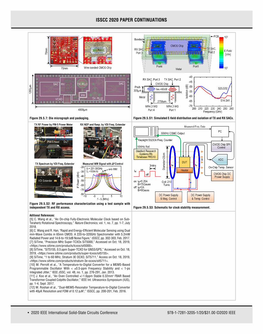
Figure 29.5.7: Die micrograph and packaging. Figure 29.5.S1: Simulated E-field distribution and isolation of TX and RX SACs.
Figure 29.5.S2: RF performance characterization using a test sample withindependent TX and RX access.
Aditional References:[5] C. Wang et al., “An On-chip Fully-Electronic Molecular Clock based on Sub-Terahertz Rotational Spectroscopy,” Nature Electronics, vol. 1, no. 7, pp. 1-7, July2018.[6] C. Wang and R. Han, "Rapid and Energy-Efficient Molecular Sensing using Dualmm-Wave Combs in 65nm CMOS: A 220-to-320GHz Spectrometer with 5.2mWRadiated Power and 14.6-to-19.5dB Noise Figure," ISSCC, pp. 302-303, Feb. 2017.[7] SiTime, “Precision MHz Super-TCXOs SiT5000,” Accessed on Oct. 18, 2019,<https://www.sitime.com/products/tcxos/sit5000>.[8] SiTime, “SiT5155, 0.5 ppm Super-TCXO for GNSS/GPS,” Accessed on Oct. 18,2019, <https://www.sitime.com/products/super-tcxos/sit5155>.[9] SiTime, “1 to 60 MHz, Stratum 3E OCXO, SiT5711,” Access on Oct. 18, 2019,<https://www.sitime.com/products/stratum-3e-ocxos/sit5711>.[10] M. Perrott et al., “A Temperature-to-Digital Converter for a MEMS-BasedProgrammable Oscillator With < ±0.5-ppm Frequency Stability and < 1-psIntegrated Jitter,” IEEE JSSC, vol. 48, no. 1, pp. 276-291, Jan. 2013.[11] J. Koo et al., “An Oven Controlled +/-1.6ppm Stable 0.32mm3 FBAR BasedTransformer Coupled Colpitts Oscillator,” IEEE Int. Ultrasonics Symposium (IUS),pp. 1-4, Sept. 2017.[12] M. Roshan et al., “Dual-MEMS-Resonator Temperature-to-Digital Converterwith 40μK Resolution and FOM of 0.12 pJK2,” ISSCC, pp. 200-201, Feb. 2016.
Figure 29.5.S3: Schematic for clock stability measurement.