Embed Size (px)
Citation preview

University of Massachusetts AmherstScholarWorks@UMass Amherst
Masters Theses 1911 - February 2014
2008
Supply Current Modeling and Analysis of DeepSub-Micron Cmos CircuitsTariq B. AhmadUniversity of Massachusetts Amherst
Follow this and additional works at: https://scholarworks.umass.edu/theses
This thesis is brought to you for free and open access by ScholarWorks@UMass Amherst. It has been accepted for inclusion in Masters Theses 1911 -February 2014 by an authorized administrator of ScholarWorks@UMass Amherst. For more information, please [email protected].
Ahmad, Tariq B., "Supply Current Modeling and Analysis of Deep Sub-Micron Cmos Circuits" (2008). Masters Theses 1911 - February2014. 82.Retrieved from https://scholarworks.umass.edu/theses/82

SUPPLY CURRENT MODELING AND ANALYSIS OF DEEP SUB-MICRON
CMOS CIRCUITS
A THESIS PRESENTED
by
TARIQ BASHIR AHMAD
Submitted to the Graduate School of the
University of Massachusetts Amherst in partial fulfillment
of the requirements for the degree of
MASTER OF SCIENCE IN ELECTRICAL AND COMPUTER ENGINEERING
February 2008
Electrical and Computer Engineering

SUPPLY CURRENT MODELING AND ANALYSIS OF DEEP SUB-MICRON
CMOS CIRCUITS
A THESIS PRESENTED
by
TARIQ BASHIR AHMAD
Approved as to style and content by:
__________________________________
Sandip Kundu, Chair
__________________________________
Wayne P. Burleson, Member
__________________________________
Maciej Ciesielski, Member
__________________________________________
C.V Hollot, Department Head
Electrical and Computer Engineering

DEDICATION
Dedicated to my beloved mother, who passed away on April 26, 2007
(May her soul rest in Eternal Peace (AMIN!)
The Fulbright Foundation and
Faisal M.Kashif

iv
ABSTRACT
SUPPLY CURRENT MODELING AND ANALYSIS OF DEEP SUB-MICRON
CMOS CIRCUITS
FEBRUARY 2008
TARIQ BASHIR AHMAD
B.S. E.E, GHULAM ISHAQ KHAN INSTITUTE OF ENGINEERING
SCIENCES, PAKISTAN.
M.S. E.C.E, UNIVERSITY OF MASSACHUSETTS AMHERST
Directed by: Professor Sandip Kundu
Continued technology scaling has introduced many new challenges in VLSI
design. Instantaneous switching of the gates yields high current flow through them that
causes large voltage drop at the supply lines. Such high instantaneous currents and
voltage drop cause reliability and performance degradation. Reliability is an issue as
high magnitude of current can cause electromigration, whereas, voltage drop can slow
down the circuit performance. Therefore, designing power supply lines emphasizes the
need of computing maximum current through them. However, the development of
digital integrated circuits in short design cycle requires accurate and fast timing and
power simulation. Unfortunately, simulators that employ device modeling methods,
such as HSPICE are prohibitively slow for large designs. Therefore, methods which can
produce good maximum current estimates in short times are critical. In this work a

v
compact model has been developed for maximum current estimation that speeds up the
computation by orders of magnitude over the commercial tools.

vi
TABLE OF CONTENTS
ABSTRACT............................................................................................................... iv
LIST OF TABLES...................................................................................................viii
LIST OF FIGURES ...................................................................................................ix
CHAPTER
1. INTRODUCTION ..................................................................................................1
1.1 Motivation ..........................................................................................................1
1.2 Background ........................................................................................................3
1.3 Where does this work fits in?.............................................................................5
2. PREVIOUS WORK................................................................................................6
2.1 Survey of analytical current modeling methods ................................................6
2.2 Survey of maximum current estimation techniques...........................................8
3. NEW APPROACH OF MODELING SUPPLY CURRENT COMPONENTS ..12
3.1 Proposed Modeling approach ..........................................................................12
3.2 New Model.......................................................................................................14
4. APPLICATION OF NEW APPROACH OF MODELING SUPPLY
CURRENT COMPONENTS................................................................................19
4.1 Environment set up ..........................................................................................19
4.1.1 Lookup Table (LUT) generation....................................................20
4.1.2 Circuit translation into 2-input NAND gates ................................. 20
4.1.3 Capacitance extraction ................................................................... 21
4.2 Application.....................................................................................................244
4.3 Algorithm......................................................................................................... 24
5. SIMULATION OF ISCAS-85 BENCHMARKS USING NEW MODELING
APPROACH ..........................................................................................................26
vii
5.1 Simulation of ISCAS-85 benchmarks with 250nm
Technology(vdd = 2.5V)..................................................................................27
5.1.1 Simulation Using Algorithm 1.......................................................27
5.1.2 Simulation using Algorithm 2........................................................37
5.2 Simulation of ISCAS-85 Benchmarks with 90nm
Technology (vdd = 1.5V).................................................................................46
5.2.1 Simulation using Algorithm 1........................................................46
5.2.2 Simulation using Algorithm 2........................................................55
5.3 Simulation of ISCAS-85 benchmarks with 65nm technology
(vdd = 1.5V).....................................................................................................64
5.3.1 Simulation using Algorithm 2........................................................64
6. CONCLUSION.....................................................................................................73
6.1 Comparing run time of new proposed model with hspice ...............................73
6.1.1 Comparing C432 Run time in HSPICE and New Model ..............73
6.1.2 Comparing C880 Run time in HSPICE and New Model ..............74
6.1.3 Comparing C2670 Run time in HSPICE and New Model ............74
6.1.4 Comparison C3540 run time in HSPICE and New Model ............75
6.1.5 Comparison of C6288 run time in HSPICE and New Model........76
6.1.6 Comparison of C7552 run time in HSPICE and New Model........76
6.2 Comparing accuracy of results between HSPICE and New Model.................77
6.2.1 Comparing accuracy between HSPICE and Algorithm1 in New
Model for 250nm technology......................................................78
6.2.2 Comparing accuracy between HSPICE and Algorithm2 in New
Model for 250nm technology......................................................79
6.2.3 Comparing accuracy between HSPICE and Algorithm1 in New
Model for 90nm technology........................................................80
6.2.4 Comparing accuracy between HSPICE and Algorithm2 in New
Model for 90nm technology........................................................81
6.2.5 Comparing accuracy between HSPICE and Algorithm2 in New
Model for 65nm technology........................................................82
6.3 Future work......................................................................................................83
BIBLIOGRAPHY ....................................................................................................84

viii
LIST OF TABLES
Table Page
1. ISCAS 85 Benchmarks description ........................................................................ 26

ix
LIST OF FIGURES
Figure Page
1. Current consumption trends in Intel Microprocessors. Source Intel ............................ 1
2. Power density trends in Intel microproccessors. Source Intel ...................................... 2
3. Power supply droop illustration .................................................................................... 3
4. Effective input signal as the as the average of the inputs ............................................. 7
5. Illustration of load current in gate network................................................................. 12
6. Components of new compact model of capturing switching current
waveform ............................................................................................................... 13
7. Compact modeling approach with 2-input NAND gate with buffer at
inputs......................................................................................................... ……….15
8. Fall case1(b) Shows input and output transitions, current from the vdd supply and
current to the ground......................... …………………………………………….16
9. Fall case2. (b) Shows input and output transitions, current from the vdd supply and
current to the ground...... …………………………………………………………16
10. Rise case1. (b) Shows input and output transitions, current from the vdd supply and
current to the ground................. ………………………………………………….17
11. Rise case2. (b) Shows input and output transitions, current from the vdd supply and
current to the ground.................. …………………………………………………17
12. Flow of steps in the environment setup ................ …………………………………19
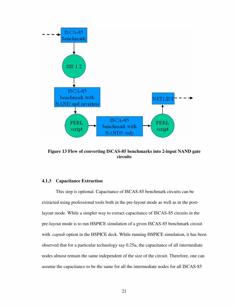
13. Flow of converting ISCAS-85 benchmarks into 2-input NAND gate circuits . ……21
14. Flow diagram of application of New Modeling approach to circuits ................... …23
15. Levelized simulation example .................................................. ……………………25
16. Flow diagram of algorithm ....................... …………………………………………25
17. Flow of Validation ............ …………………………………………………………27
18. Comparison of C17 benchmark using Algorithm1 in New Model and
HSPICE.............................................................................................................. …28

x
19.Comparison of C432 benchmark using Algorithm1 in New Model and HSPICE .... 29
20. Comparison of C880 benchmark using Algorithm1 in New Model and HSPICE .. 30
21. Comparison of C1908 benchmark using Algorithm1 in New Model and
HSPICE................................................................................................................. 31
22. Comparison of C2670 benchmark using Algorithm1 in New Model and
HSPICE................................................................................................................. 32
23. Comparison of C3540 benchmark using Algorithm1 in New Model and
HSPICE.................................................................................................................. 33
24. Comparison of C6288 benchmark using Algorithm1 in New Model and
HSPICE.................................................................................................................. 34
25. Comparison of C7552 benchmark using Algorithm1 in New Model and
HSPICE................................................................................................................. 35
26. Histogram of comparison of vdd current between Algorithm 1 in New Model and
HSPICE.. …………………………………………………………………………36
27. Histogram of comparison of ground current between Algorithm 1 in New Model
and HSPICE........................................................................................................... 36
28. Comparison of C17 Benchmark using Algorithm2 in New Model and
HSPICE................................................................................................................. 37
29. Comparison of C432 Benchmark using Algorithm2 in New Model and
HSPICE.................................................................................................................. 38
30. Comparison of C880 Benchmark using Algorithm2 in New Model and
HSPICE.................................................................................................................. 39
31. Comparison of C1908 Benchmark using Algorithm2 in New Model and
HSPICE.................................................................................................................. 40
32. Comparison of C2670 Benchmark using Algorithm2 in New Model and
HSPICE.................................................................................................................. 41
33. Comparison of C3540 Benchmark using Algorithm2 in New Model and
HSPICE.................................................................................................................. 42
34. Comparison of C6288 Benchmark using Algorithm2 in New Model and
HSPICE.................................................................................................................. 43

xi
35. Comparison of C7552 Benchmark using Algorithm2 in New Model and
HSPICE.................................................................................................................. 44
36. Comparison of vdd current in ISCAS-85 benchmarks using Algorithm2................ 45
37. Comparison of ground current in ISCAS-85 benchmarks using Algorithm2........... 45
38. Comparison of C17 Benchmark using Algorithm 1 in New Model and
HSPICE (90nm) .................................................................................................... 46
39. Comparison of C432 Benchmark using Algorithm 1 in New Model and
HSPICE (90nm) ..................................................................................................... 47
40. Comparison of C880 Benchmark using Algorithm 1 in New Model and
HSPICE (90nm) .................................................................................................... 48
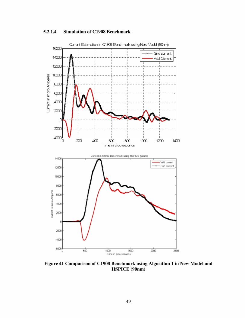
41. Comparison of C1908 Benchmark using Algorithm 1 in New Model and
HSPICE (90nm) .................................................................................................... 49
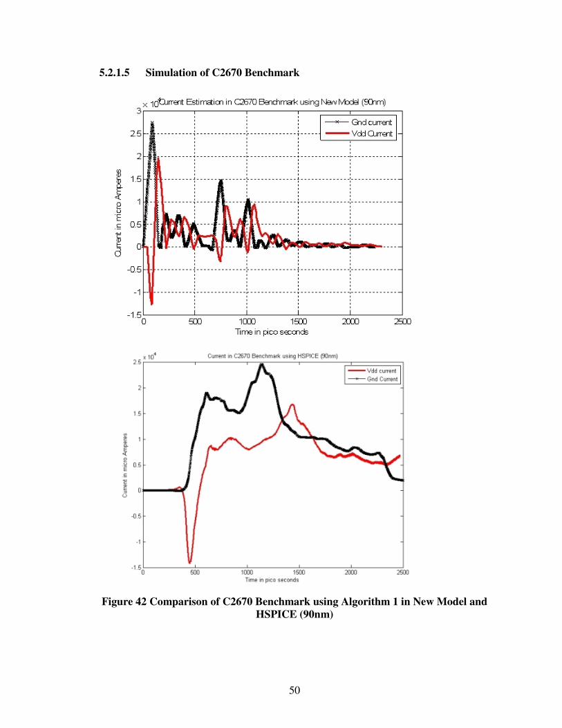
42. Comparison of C2670 Benchmark using Algorithm 1 in New Model and
HSPICE (90nm) .................................................................................................... 50
43. Comparison of C3540 Benchmark using Algorithm 1 in New Model and
HSPICE (90nm) .................................................................................................... 51
44. Comparison of C6288 Benchmark using Algorithm 1 in New Model and
HSPICE (90nm) .................................................................................................... 52
45. Comparison of C7552 Benchmark using Algorithm 1 in New Model and
HSPICE (90nm) .................................................................................................... 53
46. Histogram of comparison of vdd current using Algorithm 1 in New Model
and HSPICE for 90nm technology ........................................................................ 54
47. Histogram of comparison of ground current using Algorithm 1 in New Model
and HSPICE for 90nm technology ....................................................................... 54
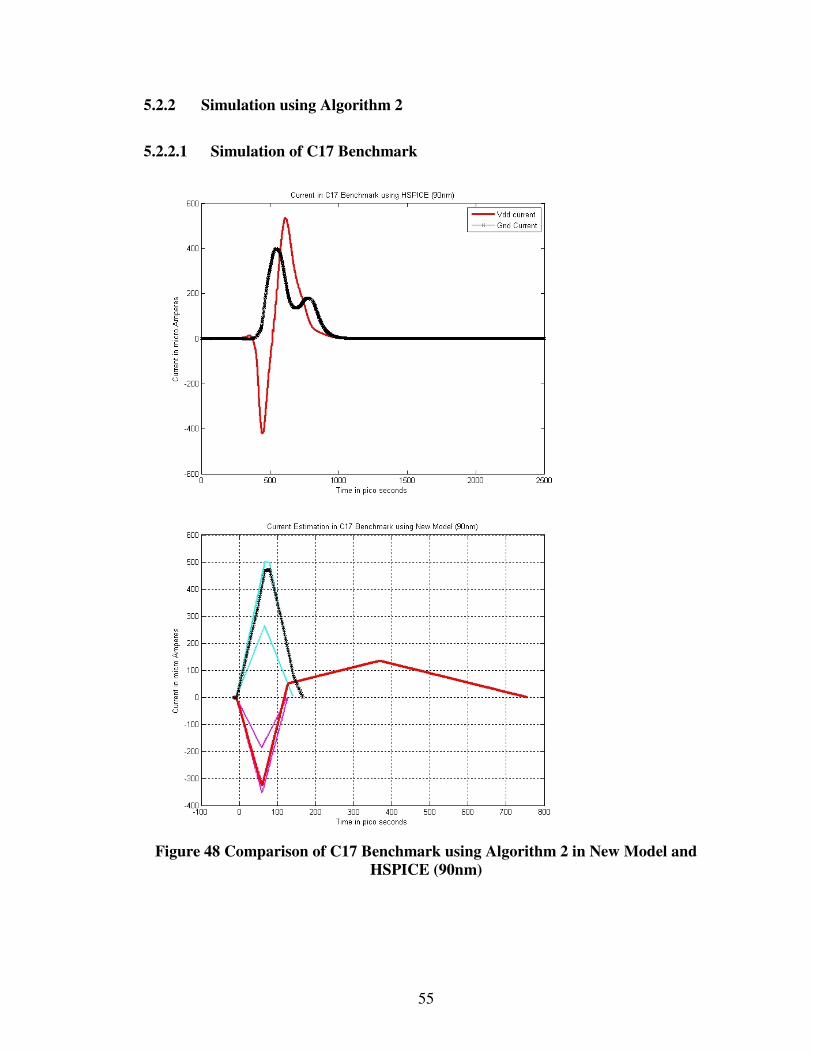
48. Comparison of C17 Benchmark using Algorithm 2 in New Model and
HSPICE (90nm) ..................................................................................................... 55
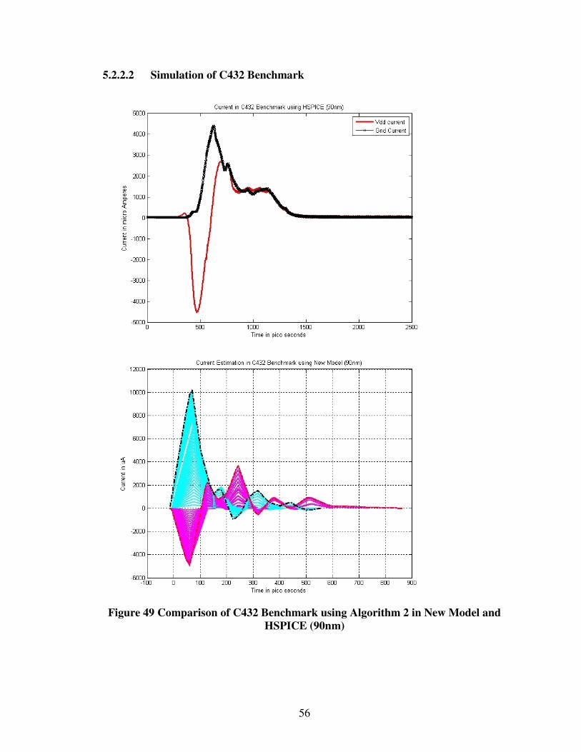
49. Comparison of C432 Benchmark using Algorithm 2 in New Model and
HSPICE (90nm) ..................................................................................................... 56
50. Comparison of C880 Benchmark using Algorithm 2 in New Model and
HSPICE (90nm) ..................................................................................................... 57

xii
51. Comparison of C1908 Benchmark using Algorithm 2 in New Model and
HSPICE (90nm) ..................................................................................................... 58
52. Comparison of C2670 Benchmark using Algorithm 2 in New Model and
HSPICE (90nm) ..................................................................................................... 59
53. Comparison of C3540 Benchmark using Algorithm 2 in New Model and
HSPICE (90nm) ..................................................................................................... 60
54. Comparison of C6288 Benchmark using Algorithm 2 in New Model and
HSPICE (90nm) ..................................................................................................... 61
55. Comparison of C7552 Benchmark using Algorithm 2 in New Model and
HSPICE (90nm) ..................................................................................................... 62
56. Histogram of Comparison of vdd current using Algorithm2 in New Model and
HSPICE (90nm) ..................................................................................................... 63
57. Histogram of Comparison of ground current using Algorithm2 in New
Model and HSPICE (90nm)................................................................................... 63
58. Comparison of C17 Benchmark using Algorithm 2 in New Model and
HSPICE (65nm) .................................................................................................... 64
59. Comparison of C432 Benchmark using Algorithm 2 in New Model and
HSPICE (65nm) ..................................................................................................... 65
60. Comparison of C880 Benchmark using Algorithm 2 in New Model and
HSPICE (65nm) ..................................................................................................... 66
61. Comparison of C1908Benchmark using Algorithm 2 in New Model and
HSPICE (65nm) ..................................................................................................... 67
62. Comparison of C2670 Benchmark using Algorithm 2 in New Model and
HSPICE (65nm) ..................................................................................................... 68
63. Comparison of C3540 Benchmark using Algorithm 2 in New Model and
HSPICE (65nm) ..................................................................................................... 69
64. Comparison of C6288 Benchmark using Algorithm 2 in New Model and
HSPICE (65nm) ..................................................................................................... 70
65. Comparison of C7552 Benchmark using Algorithm 2 in New Model and
HSPICE (65nm) ..................................................................................................... 71
xiii
66. Histogram of comparison of vdd current using Algorithm 2 in New Model and
HSPICE for 65nm technology ............................................................................... 72
67. Histogram of comparison of ground current using Algorithm 2 in New Model
and HSPICE for 65nm technology ........................................................................ 72
68. Comparison of run time of C432 with HSPICE and New Model............................. 74
69. Comparison of run time of C880 with HSPICE and New Model............................. 74
70. Comparison of run time of C2670 with HSPICE and New Model........................... 75
71. Comparison of run time of C3540 with HSPICE and New Model........................... 75
72. Comparison of run time of C6288 with HSPICE and New Model........................... 76
73. Comparison of run time of C7552 with HSPICE and New Model........................... 77
74. Mean square error in vdd current between HSPICE and Algorithm 1 in
New Model (250nm)............................................................................................. 78
75. Mean square error in ground current between HSPICE and Algorithm 1 in New
Model (250nm) .. …………………………………………………………………78
76. Mean square error in vdd current between HSPICE and Algorithm 2 in
New Model (250nm)............................................................................................. 79
77. Mean square error in ground current between HSPICE and Algorithm 2 in New
Model (250nm) ...................................................................................................... 79
78. Mean square error in vdd current between HSPICE and Algorithm 1 in
New Model (90nm)............................................................................................... 80
79. Mean square error in ground current between HSPICE and Algorithm 1 in
New Model (90nm)............................................................................................... 80
80. Mean square error in vdd current between HSPICE and Algorithm 2 in
New Model (90nm)............................................................................................... 81
81. Mean square error in ground current between HSPICE and Algorithm 2 in
New Model (90nm)................................................................................................ 81
82. Mean square error in vdd current between HSPICE and Algorithm 2 in
New Model (65nm)............................................................................................... .82

xiv
83. Mean square error in ground current between HSPICE and Algorithm 2 in New
Model (65nm) ........................................................................................................ 82

1
CHAPTER 1
INTRODUCTION
1.1 Motivation
As Moore’s law continues to hold today, the numbers of transistors per chip
continue to grow per generation. As a result gate density increases per generation. An
increase in gate density translates into more switching activity. At the same time,
voltage gets scaled down per generation. This voltage scaling contributes to faster
switching of the transistors which leads to high frequency and thus improved
performance. These two trends have led to an increase in the current consumption of a
chip. Even though an increase in current consumption is followed by voltage scaling
and reduction in transistor size, the net effect is still a huge increase in the current
consumption as shown in Figure 1
Figure 1 Current consumption trends in Intel Microprocessors. Source Intel

2
This unintended consequence of Moore’s law has led to an exponential increase
in current and power densities per generation. Power density has been increasing as
much as 80 % per generation while current density has been increasing as much as 225
% per generation. See Figure 2 for power density trend.
Figure 2 Power density trends in Intel microprocessors. Source Intel
Power distribution network has not been able to cope up with these trends
resulting in compromise in the power delivery such that the power distribution network
becomes a bottleneck [1].
Another consequence of Moore’s law is the interconnect scaling. The
interconnects are becoming more resistive per generation. When large current flows
through such thin interconnect lines, it causes voltage drop termed as IR drop. This IR
drop manifests itself as glitch on power distribution lines and causes erroneous logic
signals (soft errors) and degradation in switching speed. Further, high sustained current
flow can cause electromigration.

3
In short, in order to avoid logic errors, the circuit needs to be redesigned to
mitigate IR drop and reduced noise margins. This highlights the need for efficient CAD
tools to estimate IR drop in the power distribution lines. The first step in solving this
problem is quantifying the IR drop, which is also referred as droop, which is slack in
power supply voltage below its nominal value. See Figure 3
Figure 3 Power supply droop illustration
This droop depends upon the switching pattern. To quantify the droop requires
modeling switching current waveform, which itself depends upon output load and input
drive. Hence modeling worst case switching current will allow us to compute the worst
case droop and size the supply lines accordingly. This work is about compact modeling
of this switching current waveform and using it to estimate the total supply currents, i.e.
supply (vdd) current and ground current.
1.2 Background
Power is distributed to electronic components in an integrated circuit over a
network of conductors. Power network design is about designing such power
distribution networks with adequate performance and reliability.
time
DDDDrooprooprooproop
VddVddVddVdd

4
IR drop across the network causes the voltage seen by the device to be supply
voltage – IR drop. Another kind of voltage drop is caused by package inductance. It is
commonly referred as di/dt drop. Therefore, the voltage seen by the device gets further
reduced by this quantity.
To mitigate voltage drop at supply lines, capacitance is inserted between power
and ground lines referred as decoupling capacitance or decaps. It acts as local charge
storage and is helpful in counteracting voltage drop at supply points. However, given
the high frequency switching of today’s integrated circuits, decoupling capacitor does
not provide much relief. Further, parasitic interconnect resistance, decoupling
capacitance and package inductance form a complex RLC network with its own
resonance frequency. If the resonance frequency gets anywhere close to the frequency
of the integrated circuit, large voltage drop can occur.
Another issue in the analysis of power distribution network is the large size of
integrated circuit in terms of electronic components. Simulating all such devices is
infeasible. Such simulation requires searching for a pattern that causes maximum
switching. A circuit with n inputs requires searching among 22n
patterns which is NP
complete problem. An important consideration in the analysis of power distribution
network is what these patterns should be. For IR drop, pattern or patterns that cause
maximum switching are required. While for electromigration, patterns that cause large
sustained current are of interest.
Power grid analysis can be classified into input vector dependent methods and
vectorless methods. 1)The input vector pattern dependent methods employ search
techniques to find a set of input patterns which cause the worst drop in the grid. A

5
number of methods have been proposed in literatures which use genetic algorithms or
other search techniques to find vectors or a pattern of vectors that maximize the total
current drawn from the supply network. Input vector-pattern dependent approaches are
computationally intensive. Furthermore, these approaches are inherently optimistic,
underestimating the voltage drop and thus letting some of the supply noise problems go
unnoticed. 2) The vectorless approaches, on the other hand, aim to compute an upper
bound on the worst-case drop in an efficient manner. These approaches have the
advantage of being fast and conservative, but are sometimes too conservative, leading to
overdesign [5,6].
1.3 Where does this work fits in?
It is mentioned in [7] that a complete power supply distribution model must
include
1) Package level power distribution network dominated by Inductance
2) On-chip power bus model dominated by Resistance
3) On-chip switching activities model for each functional block which means
determining the switching current.
From [7], it follows that our work falls in 3), which is modeling switching
current waveform of a network.

6
CHAPTER 2
PREVIOUS WORK
2.1 Survey of analytical current modeling methods
Analytical methods for estimating switching current waveform of CMOS gates
have been in use since the introduction of CMOS technology. Analytical equations exist
both for NMOS and PMOS for each region of their operation and for every technology
generation. Moving to a higher level of abstraction, CMOS inverter has been a subject
of an extended research [9-12], which is the basic block to which all CMOS circuits can
be collapsed. It has been proposed in various research studies that if one could convert a
CMOS circuit into an equivalent CMOS inverter that has the same performance, then
modeling switching current waveform of the CMOS circuit is equivalent to modeling
switching current waveform of an equivalent CMOS inverter.
Analytical modeling of CMOS inverter aim at deriving an output expression
based upon input status for each region of operation of each transistor. Various
analytical models have been proposed such as Shiman-Hodges square law [9], nth
power law [10], and Alpha power law [11-12]. They all suffer from the same problems
of complicated expressions and inability to account for deep submicron effects. Hence,
they require modification every technology generation.
In the past, estimation techniques focused upon dynamic current flow, caused by
the charging or discharging of output load capacitance. However, in the deep submicron
era, short circuit current flow can not be neglected. Exactly similar approach has been
adopted to model short circuit current as dynamic current. The CMOS circuit is

7
converted to an equivalent CMOS inverter for estimating short circuit current. The
problem here is to determine the size of transistors in the CMOS inverter as well as the
effective input signal fed to it. The approach has been to choose fastest input signal as
the effective signal for parallel connected MOSFETS and vice versa [15]. This
approach may result in erroneous delay information [16]. Another approach of choosing
effective input signal of an equivalent CMOS inverter is to heuristically choose the
average of the overlapping signals at the inputs as shown in Figure 4. The solid lines
represent the original input signals while the dotted line represents the effective input.
Figure 4 Effective input signal as the as the average of the inputs
Similarly, effective channel width of the equivalent CMOS inverter is
calculated. Traditionally, the equivalent transistor width of MOSFETs connected in
series is the inverse of the sum of reciprocals of the channel width of each individual
transistor and vice versa for MOSFETs connected in parallel [16]. A better
approximation is proposed in [15], where the equivalent transistor width depends on the
relative delays of input signals.

8
2.2 Survey of maximum current estimation techniques
There has been an extensive research done on the estimation of currents in
power supply lines for deterministic input patterns [15, 18, 19, and 20]. The proposed
methods provide speed up over HSPICE while providing acceptable accuracy of power
and ground current waveforms. Thus finding maximum current in power distribution
lines translates to running simulation over all possible input patterns and choosing the
one that causes maximum current drawn. However, these methods can be applied to
small circuits having a few inputs. As the circuit gets larger, the number of input
patterns that can be applied grows exponentially and these methods are not practical.
Chowdhury et al [21] have addressed the problem of maximum current
estimation for large circuits with large number of inputs. In their proposed method, a
large circuit is divided into smaller logic blocks. Then either a search technique i.e.,
branch or bound or heuristic technique is employed to find maximum transient current
for every logic block. The sum of maximum transient currents for each block represents
the estimated maximum current for the entire circuit. However, their method suffers
from the problem of overestimation. Further, due to large circuit size, their search
technique is slow.
Devdas et al [22] have addressed the same problem. They formulate maximum
current estimation problem as weighted max-satisfiability problem on a set of multi-
output Boolean functions. These functions are derived from the logic description of the
circuit. Branch and bound algorithm is employed to solve this N-P complete max
satisfiability problem. However, they attempted the problem under the unit gate delay

9
assumption. Further, the output functions are quite complex and running time is slow.
They also didn’t attempt to solve for the general gate delay.
From the above survey, it is established that proposed techniques are
computationally prohibitive for large VLSI circuits. In such a case, pattern independent
algorithms become a natural choice. In the following paragraphs such techniques are
being discussed.
Previous work by Farid Najm et al [3] estimates an upper bound of maximum
current from the power supply and ground buses by propagating input excitations and
time intervals through a levelized gate network. The proposed algorithm termed as
‘iMax’ calculates maximum current waveform statistically in linear time and is pattern
independent. Hence this work has resorted to static approach of current calculation, as
simulation of a large input set for larger circuits is prohibitively expensive. However,
this work assumes all inputs are independent, all primary inputs switch at time t = 0,
circuit style is combinational, gate delays are fixed and known ahead of time, waveform
shape is right angled triangular, various parameters of the transition current waveform
such as its peak, duration and the time at which it occurs are calculated in a
preprocessing phase from the circuit level parameters of the gate under consideration as
well as of the other gates that are connected to its inputs and output. Another
assumption is that between the times at inputs when an interval begins or ends, and the
next interval begins or ends, the sets of excitations that the inputs can assume do not
change and therefore no corresponding uncertainty interval can begin or end at the
output during that time shifted by the gate delay D.

10
Work by Yi-Min Jiang [2] et al has extended the work done by Farid Najm et al
and present four approaches 1) timed-ATPG-based approach, 2) probability based
approach, 3) genetic algorithm based approach and 4) integer linear programming based
approach for estimating the maximum instantaneous currents through the supply lines.
The first three approaches produce a tight lower bound while the fourth approach an
exact solution for small circuits and tight upper bounds for large circuit. In timed-ATPG
approach, a set of signals whose simultaneous switching produces high current is
assigned transitions and timed-ATPG is used to justify the assignments and derive two-
vector sequences. But selection of such signals has not been explained and justified. In
the probability-based approach, a set of selected gates is assigned weights based on their
possible current contribution at a given time. Again, it is not specified how do they
select such gates and how do they assign weights? In the ILP-based approach, the
problem is modeled as an ILP problem. Solving the corresponding ILP formula allows
finding an exact solution. However, this technique is impractical for large circuits. They
propose a partition solution for breaking the bigger circuit into smaller sub-circuits and
solving ILP for smaller sub-circuits. However, the upper bound found by combining the
ILP solutions of sub-circuits is not a tight upper bound. In the genetic algorithm-based
(GA) approach, which works at any level of abstraction unlike the previous three
approaches that work at the gate level, a search is conducted based on mechanics of
natural selection and natural genetics. To use GA, elements in the solution space are
coded into finite length strings. Each string has a fitness values associated with it. But it
is not defined how to associate a fitness value with a given string. They use three
processes of 1) selection, 2) crossover and 3) mutation to generate new strings. The

11
objective is to generate strings with high fitness value. The initial population contains N
random strings of length L. The fitness value of each string is calculated by a fitness
function. Generation of a new population is found by selecting two individuals from the
current population, crossing the two selected strings, and mutating the elements of the
new strings with a given mutation probability. The process is repeated until the number
of strings in the new population is equal to N. Selection is biased toward individuals
with higher fitness values so the average fitness value tends to increase. The next
population is generated based on the current population using the same procedure. The
process continues until the number of generations reaches a predefined value, or the
optimal solution has been found.

12
CHAPTER 3
NEW APPROACH OF MODELING SUPPLY CURRENT COMPONENTS
3.1 Proposed Modeling approach
On the basis of discussion presented in chapter 1, it is established that power
supply droop is a dynamic quantity that depends upon the current drawn by the output
load also known as load current. This current itself depends upon the output load and
input drive. Therefore, modeling load current waveform of a switching network is equal
to modeling load current at each and every gate in the network. This idea is illustrated
in figure 5
SOLID is switching Vdd current DASHED is switching ground current
Figure 5 Illustration of load current in gate network
Modeling load current requires that load current has a certain associated
waveform. In this chapter, a compact model is presented to capture this waveform.
Gnd
Vdd

13
Once this waveform is captured for each gate based on its switching status, they can be
added to get the the total switching current waveform.
In our new compact model, switching current waveform is a function of
1) Output load capacitance l at the output of a gate
2) Input voltage v at the gate and
3) Slope s of the transition at the input of the gate.
This is illustrated in the case of a 2-input NAND gate in figure 6.
Figure 6 Components of new compact model of capturing switching current
waveform
Hence,
switching( , , )I function l v s= Equation 1
Similarly peak supply current is defined by the following equation
Vdd
Output load
capacitance
slope
slope
slope
We are
interested
in current
waveforms
through
these lines

14
Equation 2
For characterizing peak current and total supply current consumption, a vector
based circuit simulation is used to find the total supply currents i.e both ground and vdd
currents. Unlike the work done by Farid Najm et al [3] and Angela Krystic et al [4],
dynamic simulation is used to compute vdd and ground currents for a gate network
given a specific input pattern. This is intended to eliminate the need of using HSPICE,
which is slow for large circuits and works at a lower level of abstraction. Moreover,
HSPICE solves complex differential equations while our compact model uses a simple
approach of characterizing switching current waveform as a function of load, slope and
input voltage. If working with a particular technology for example 0.25 micron, the
supply voltage is known to be 2.5 volts so one can skip voltage, as it is constant and
model switching current waveform as a function of slope and output load capacitance.
3.2 New Model
To compute switching current waveform of a gate in a network, we use compact
modeling approach applied to a 2-input NAND gate with buffer at inputs as our model
shown in figure 7. It should be noted that a 2-input NAND gate is chosen because it is a
universal gate and many technology mapping tools such as SIS can convert a
heterogeneous gate network into a network of only 2-input NAND gates. But
nevertheless, our compact modeling approach can be applied to other gate types as well.
This part is being skipped here because of the enormity of this.
1
_ max max( _ )
gates
i
peak current switching currents=
= ∑

15
NAND Gate ModelCurrent I = func(output load,input slope,input voltage)
Figure 7 Compact modeling approach with 2-input NAND gate with buffer at
inputs
The New Model is driven with particular load capacitance at the output, slope
and voltage at the input. The New Model is used to compute vdd and gnd currents for
different voltages, slopes and load combinations. Note that we are not interested in the
current through load capacitance but the total current from the vdd and ground buses.
The New Model is not only used to compute peak values of these currents but also
propagation delay, width of the current waveforms and output slope. This way one can
capture the whole current waveform.
There are four transition cases for a 2-input NAND gate that cause transition at
its output: two for the fall transition and two for the rise transition. The two fall
transitions are
1) When one of the input changes from 0 to 1 while the other remains at 1 as shown in
figure 8 along with the currents that flow from vdd supply and sink in the ground.

16
(a) (b)
Figure 8 Fall case1. (b) Shows input and output transitions, current from the vdd
supply and current to the ground
.
2) When both of the inputs change from 0 to 1 as shown in figure 9
(a) (b)
Figure 9 Fall case2. (b) Shows input and output transitions, current from the vdd
supply and current to the ground.
Vdd
Output load
capacitance
slope
slope
1-1

17
Similarly the two rise transitions are
1) When one of the input changes from 1 to 0 while the other remains at 1 as
shown in figure 10.
(a) (b)
Figure 10 Rise case1. (b) Shows input and output transitions, current from the vdd
supply and current to the ground.
2) When both of the inputs change from 1 to 0 as shown in figure 11
(a) (b)
Figure 11 Rise case2. (b) Shows input and output transitions, current from the vdd
supply and current to the ground.

18
In the case when output does not switch, a slightly different approach of modeling is
used which will be discussed later.

19
CHAPTER 4
APPLICATION OF NEW APPROACH OF MODELING SUPPLY CURRENT
COMPONENTS
Now that a compact model of supply currents has been defined, it is necessary to
apply this to circuits. But before its application, there are certain steps that should be
followed. These steps are called setting up the environment.
4.1 Environment set up
The environment set up consists of three major steps. The following flow
diagram describes the three steps.
Figure 12 Flow of steps in the environment setup
Capacitance extraction
LUT generation
Circuit conversion into 2-input NAND
gates

20
4.1.1 Lookup Table (LUT) generation
Based on the basis of experiments on a 2-input NAND gate detailed in
Appendix A, four lookup tables (LUTs) were generated for the four switching cases.
These experiments helped simplify the lookup tables as much as possible. A lookup
table is generated for each switching case by keeping slope/s and arrival time/s fixed
while varying the output load capacitance. This translates to running HSPICE
simulations by just varying the output load and capturing the values that can help plot
supply current waveforms. The values that are captured by this table are maximum and
minimum values of vdd current, maximum and minimum values of gnd current, widths
of the current waveforms, output slope and output delay. Note that all quantities are
dynamic.
4.1.2 Circuit translation into 2-input NAND gates
As discussed in the previous chapter, the model is based on 2-input NAND gate.
Hence one can apply this new model onto a 2-input NAND gate network. So either one
can build a 2-input NAND gate network from the scratch or convert widely used
ISCAS-85 benchmarks to 2-input NAND gates. Following is the flow of converting
ISCAS-85 benchmarks to 2-input NAND gates. It should be noted that the proposed
model can be applied to other types of gates with different fan in besides a 2 input
NAND gate but this part is being skipped because of the enormity of this project and
time constraint.
21
Figure 13 Flow of converting ISCAS-85 benchmarks into 2-input NAND gate
circuits
4.1.3 Capacitance Extraction
This step is optional. Capacitance of ISCAS-85 benchmark circuits can be
extracted using professional tools both in the pre-layout mode as well as in the post-
layout mode. While a simpler way to extract capacitance of ISCAS-85 circuits in the
pre-layout mode is to run HSPICE simulation of a given ISCAS-85 benchmark circuit
with .captab option in the HSPICE deck. While running HSPICE simulation, it has been
observed that for a particular technology say 0.25u, the capacitance of all intermediate
nodes almost remain the same independent of the size of the circuit. Therefore, one can
assume the capacitance to be the same for all the intermediate nodes for all ISCAS-85

22
benchmarks. This assumption greatly reduces the computation time to be discussed later
on.
4.2 Application
The following flow diagram in Figure 14 describes the application of proposed
New Model to circuits. In order to apply the proposed New Model, all circuit
information should be provided to the Model as input. This includes providing primary
inputs, primary outputs, gate delay information, load capacitance information, netlist
and input pattern for a circuit. The other information that needs to be provided to the
New Model is the Lookup Tables (LUT) which is global for a certain technology. Once
all this information is presented to the New Model, it processes the information
according to an algorithm (to be discussed in the next section) to compute switching
current values, widths of switching current waveforms and output gate delay. Once all
switching gates are processed in such a manner, waveforms are constructed for each
such gate. Both vdd and ground current waveforms are constructed per switching gate.
For simplicity, triangular construction is used for both vdd and ground waveforms.
Once all these waveforms have been constructed for all switching gates, superposition
is applied to superpose all ground waveforms to get one final ground waveform.
Similarly, superposition is applied to all vdd waveforms to get one final vdd waveform.
The maximum values of these two waveforms estimate the maximum vdd and ground
current for a particular pattern in a circuit. Figure 14 also shows an optional step, which
is superposition of nonswitching waveforms into the switching waveforms. Non-
switching waveform is generated for a 2 input NAND gate when both the inputs make a
transition while the output does not make a transition. For example when one input of a

23
2 input NAND switches from zero to one while the other input of the NAND gate
switches from one to zero. In this case, one can add the contribution of such gates by
counting the number of such gates and scaling the final ground waveform appropriately.
Figure 14 Flow diagram of application of New Modeling approach to circuits.
Delay Info
Netlist LUT Input Pattern
PI PO Output Load
Algorithm
Current waveform
widths
Switching current values
(max/min)
Output Delay
Triangular construction of
vdd & gnd current waveforms
Superposition of waveforms
Final vdd & gnd current
waveforms

24
4.3 Algorithm
Figure 16 discusses the flow of the algorithm which is the core of application of
proposed New Modeling approach to the circuits. The algorithm makes several arrays
out of the information that is provided to the application as input. The algorithm then
calls a procedure Evaluate_Netlist that first initializes all arrays to a condition that
marks that no gate has been evaluated. The algorithm then enters into a loop which
iterates until all gates are evaluated. The order in which gates are evaluated is levelized
order shown in figure 15. Levelized order makes sure that a gate is not evaluated until
all of its inputs have arrived. Therefore, gates at level 0 are evaluated first then gates at
level 1 and so on until all gates have been evaluated. Coming back to the algorithm,
when inside the loop, for every gate input transitions are obtained based upon the input
pattern. Based upon this information, algorithm falls into one of four switching cases
and fetches information from the appropriate Lookup table (LUT) based upon load
information. The information obtained from the LUT is used to fill delay and switching
waveform arrays. Based upon this information, triangular waveforms are constructed
for all switching gates. Once all gates have been evaluated, algorithm exits out of the
loop, superposition is done on all vdd waveforms and ground waveforms to get one
final vdd waveform and one final ground waveform. The maximum values of vdd
waveform and ground waveform estimate the maximum vdd and maximum ground
current respectively.

25
Level 0 Level 1 Level 2 Level 3
Figure 15 Levelized simulation example
Figure 16 Flow diagram of algorithm
Gate level Netlist
Load Cap
Information
SimulationModel
Input PatternInformation
Delay/slopeEquations
CompactCurrent Model
Switching Node/Timing information
TimingWheel
Simulation
Triangular CurrentConstruction & Superposition
CurrentEnvelope
Gate level Netlist
Load Cap
Information
SimulationModel
Input PatternInformation
Delay/slopeEquations
CompactCurrent Model
Switching Node/Timing information
TimingWheel
Simulation
Triangular CurrentConstruction & Superposition
CurrentEnvelope

26
CHAPTER 5
SIMULATION OF ISCAS-85 BENCHMARKS USING NEW MODELING
APPROACH
Now that an application environment has been setup for the proposed New
Current Model, its time to apply this to real circuits. The circuit suite chosen for this
purpose is ISCAS-85 benchmarks. Following Table 1 describes the ISCAS-85
benchmarks. Please note that for our purpose, ISCAS-85 benchmarks have been
converted to pure 2 input NAND gates using flow described in the previous chapter.
Circuit Name Circuit Function Total Gates # of Inputs # of outputs
C17 ALU 6 5 2
C432 Priority Decoder 347 36 7
C880 ALU & Control 540 60 26
C1908 ECAT 972 33 25
C2670 ALU & Control 1354 233 144
C3540 ALU & Control 1899 50 22
C6288 16 Bit Multiplier 2399 32 32
C7552 ALU & Control 3870 207 108
Table 1 ISCAS 85 Benchmarks description
Further, the following flow in figure 17 describes how validation will be done.
As the figure shows, a netlist for any benchmark is given to the New Proposed Model
(upper arm of the figure 17) and to a PERL script that converts that netlist into a
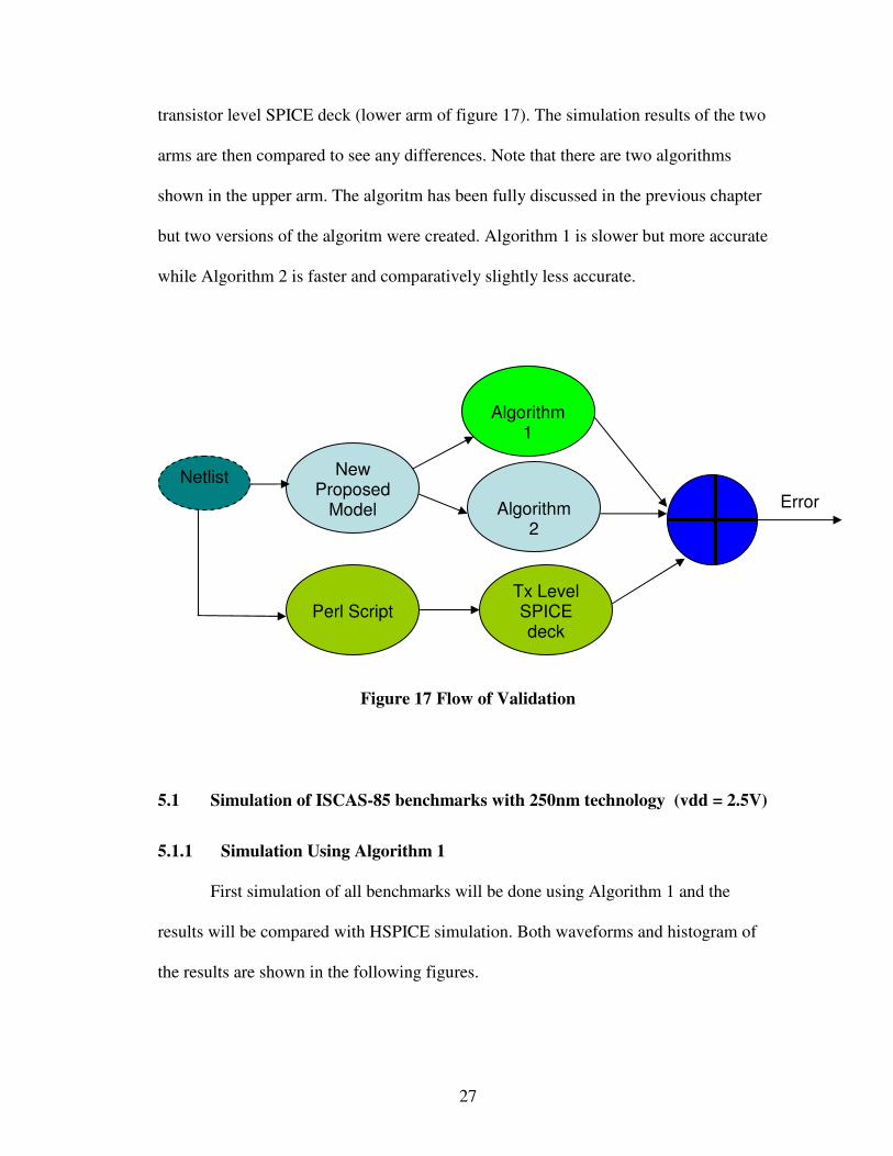
27
transistor level SPICE deck (lower arm of figure 17). The simulation results of the two
arms are then compared to see any differences. Note that there are two algorithms
shown in the upper arm. The algoritm has been fully discussed in the previous chapter
but two versions of the algoritm were created. Algorithm 1 is slower but more accurate
while Algorithm 2 is faster and comparatively slightly less accurate.
Figure 17 Flow of Validation
5.1 Simulation of ISCAS-85 benchmarks with 250nm technology (vdd = 2.5V)
5.1.1 Simulation Using Algorithm 1
First simulation of all benchmarks will be done using Algorithm 1 and the
results will be compared with HSPICE simulation. Both waveforms and histogram of
the results are shown in the following figures.
Error
Netlist New Proposed
Model
Algorithm
1
Perl Script
Tx Level SPICE deck
Algorithm
2

28
5.1.1.1 Simulation of C17 Benchmark
Figure 18 Comparison of C17 benchmark using Algorithm1 in New Model and
HSPICE

29
5.1.1.2 Simulation of C432 Benchmark
Figure 19 Comparison of C432 Benchmark using Algorithm 1 in New Model and
HSPICE

30
5.1.1.3 Simulation of C880 Benchmark
Figure 20 Comparison of C880 Benchmark using Algorithm 1 in New Model and
HSPICE

31
5.1.1.4 Simulation of C1908 Benchmark
Figure 21 Comparison of C1908 Benchmark using Algorithm 1 in New Model and
HSPICE

32
5.1.1.5 Simulation of C2670 Benchmark
Figure 22 Comparison of C2670 Benchmark using Algorithm 1 in New Model and
HSPICE

33
5.1.1.6 Simulation of C3540 Benchmark
Figure 23 Comparison of C3540 Benchmark using Algorithm 1 in New Model and
HSPICE

34
5.1.1.7 Simulation of C6288 Benchmark
Figure 24 Comparison of C6288 Benchmark using Algorithm 1 in New Model and
HSPICE

35
5.1.1.8 Simulation of C7552 Benchmark
Figure 25 Comparison of C7552 Benchmark using Algorithm 1 in New Model and
HSPICE

36
C17 C432 C880 C1908 C2670 C3540 C6288 C75520
1
2
3
4
5
6x 10
4
benchmarks
Peak V
dd C
urr
ent
in u
A
comparing ISCAS-85 Benchmarks for 0.25u technology
HSPICE
NEW MODEL
Figure 26 Histogram of comparison of vdd current between Algorithm 1 in New
Model and HSPICE
C17 C432 C880 C1908 C2670 C3540 C6288 C75520
1
2
3
4
5
6
7
8x 10
4
benchmarks
Peak G
nd C
urr
ent
in u
A
comparing ISCAS-85 Benchmarks for 0.25u technology
HSPICE
NEW MODEL
Figure 27 Histogram of comparison of ground current between Algorithm1 in New
Model and HSPICE.

37
5.1.2 Simulation using Algorithm 2
Now simulation of all benchmarks will be done using Algorithm 2 and the
results will be compared with HSPICE simulation. Both waveforms and histogram of
the results are shown in the following figures.
5.1.2.1 Simulation of C17 Benchmark
Figure 28 Comparison of C17Benchmarkusing Algorithm2 in NewModel
andHSPICE

38
5.1.2.2 Simulation of C432 Benchmark
Figure 29 Comparison of C432Benchmark using Algorithm2 in NewModel and
HSPICE
39
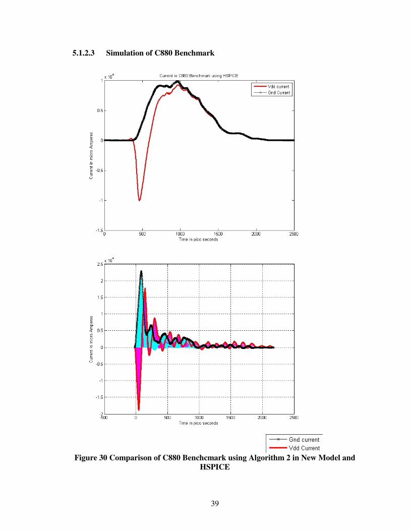
5.1.2.3 Simulation of C880 Benchmark
Figure 30 Comparison of C880 Benchcmark using Algorithm 2 in New Model and
HSPICE

40
5.1.2.4 Simulation of C1908 Benchmark
Figure 31 Comparison of C1908 Benchcmark using Algorithm 2 in New Model and
HSPICE

41
5.1.2.5 Simulation of C2670 Benchmark
Figure 32 Comparison of C2670 Benchcmark using Algorithm 2 in New Model and
HSPICE
42
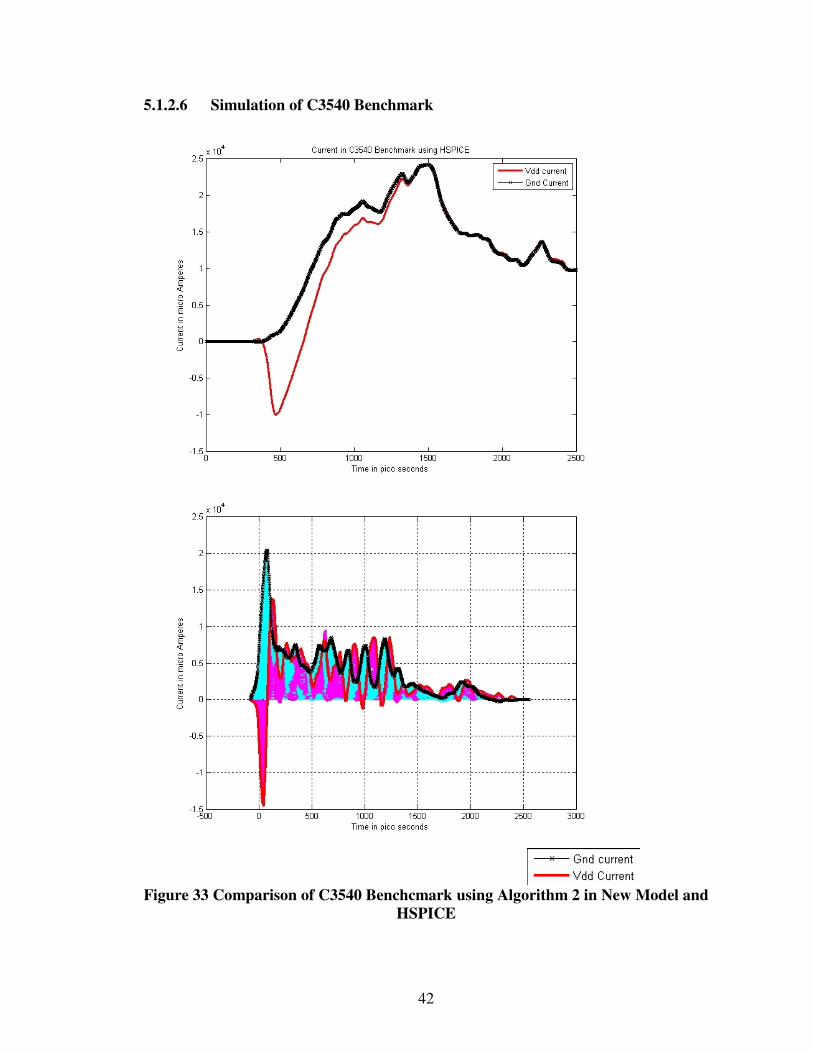
5.1.2.6 Simulation of C3540 Benchmark
Figure 33 Comparison of C3540 Benchcmark using Algorithm 2 in New Model and
HSPICE

43
5.1.2.7 Simulation of C6288 Benchmark
Figure 34 Comparison of C6288 Benchcmark using Algorithm 2 in New Model and
HSPICE

44
5.1.2.8 Simulation of C7552 Benchmark
Figure 35 Comparison of C7552 Benchcmark using Algorithm 2 in New Model and
HSPICE

45
C17 C432 C880 C1908 C2670 C3540 C6288 C75520
1
2
3
4
5
6x 10
4
benchmarks
Peak V
dd C
urr
ent
in u
A
comparing ISCAS-85 Benchmarks for 0.25u technology
HSPICE
NEW MODEL
Figure 36 Comparison of vdd current in ISCAS-85 benchmarks using Algorithm2
C17 C432 C880 C1908 C2670 C3540 C6288 C75520
1
2
3
4
5
6
7x 10
4
benchmarks
Peak G
nd C
urr
ent
in u
A
comparing ISCAS-85 Benchmarks for 0.25u technology
HSPICE
NEW MODEL
Figure 37 Comparison of ground current in ISCAS-85 benchmarks using
Algorithm2

46
5.2 Simulation of ISCAS-85 Benchmarks with 90nm Technology (vdd = 1.5V)
5.2.1 Simulation using Algorithm 1
5.2.1.1 Simulation of C17 Benchmark
Figure 38 Comparison of C17 Benchmark using Algorithm 1 in New Model and
HSPICE (90nm)

47
5.2.1.2 Simulation of C432 Benchmark
Figure 39 Comparison of C432 Benchcmark using Algorithm 1 in New Model and
HSPICE (90nm)

48
5.2.1.3 Simulation of C880 Benchmark
Figure 40 Comparison of C880 Benchmark using Algorithm 1 in New Model and
HSPICE (90nm)
49
5.2.1.4 Simulation of C1908 Benchmark
Figure 41 Comparison of C1908 Benchmark using Algorithm 1 in New Model and
HSPICE (90nm)
50
5.2.1.5 Simulation of C2670 Benchmark
Figure 42 Comparison of C2670 Benchmark using Algorithm 1 in New Model and
HSPICE (90nm)

51
5.2.1.6 Simulation of C3540 Benchmark
Figure 43 Comparison of C3540 Benchmark using Algorithm 1 in New Model and
HSPICE (90nm)

52
5.2.1.7 Simulation of C6288 Benchmark
Figure 44 Comparison of C6288 benchmark using Algorithm 1 in New Model and
HSPICE (90nm)

53
5.2.1.8 Simulation of C7552 Benchmak
Figure 45 Comparison of C7552 Benchmark using Algorithm 1 in New Model and
HSPICE (90nm)

54
C17 C432 C880 C1908 C2670 C3540 C6288 C75520
0.5
1
1.5
2
2.5
3
3.5
4
4.5x 10
4
benchmarks
Peak V
dd C
urr
ent
in u
A
comparing ISCAS-85 Benchmarks for 90nm technology, VDD = 1.5V
HSPICE
NEW MODEL
Figure 46 Histogram of comparison of vdd current using Algorithm 1 in New
Model and HSPICE for 90nm technology
C17 C432 C880 C1908 C2670 C3540 C6288 C75520
1
2
3
4
5
6x 10
4
benchmarks
Peak G
nd C
urr
ent
in u
A
comparing ISCAS-85 Benchmarks for 90nm technology, VDD = 1.5V
HSPICE
NEW MODEL
Figure 47 Histogram of Comparison of ground current using Algorithm1 in New
Model and HSPICE for 90nm technology
55
5.2.2 Simulation using Algorithm 2
5.2.2.1 Simulation of C17 Benchmark
Figure 48 Comparison of C17 Benchmark using Algorithm 2 in New Model and
HSPICE (90nm)
56
5.2.2.2 Simulation of C432 Benchmark
Figure 49 Comparison of C432 Benchmark using Algorithm 2 in New Model and
HSPICE (90nm)

57
5.2.2.3 Simulation of C880 Benchmark
Figure 50 Comparison of C880 Benchmark using Algorithm 2 in New Model and
HSPICE (90nm)

58
5.2.2.4 Simulation of C1908 Benchmark
Figure 51 Comparison of C1908 Benchmark using Algorithm 2 in New Model and
HSPICE (90nm)

59
5.2.2.5 Simulation of C2670 Benchmark
Figure 52 Comparison of C2670 Benchmark using Algorithm 2 in New Model and
HSPICE (90nm)

60
5.2.2.6 Simulation of C3540 Benchmark
Figure 53 Comparison of C3540 Benchmark using Algorithm 2 in New Model and
HSPICE (90nm)

61
5.2.2.7 Simulation of C6288 Benchmark
Figure 54 Comparison of C6288 Benchmark using Algorithm 2 in New Model and
HSPICE (90nm)

62
5.2.2.8 Simulation of C7552 Benchmark
Figure 55 Comparison of C7552 Benchmark using Algorithm 2 in New Model and
HSPICE (90nm)

63
C17 C432 C880 C1908 C2670 C3540 C6288 C75520
0.5
1
1.5
2
2.5
3
3.5
4
4.5x 10
4
benchmarks
Peak V
dd C
urr
ent
in u
A
comparing ISCAS-85 Benchmarks for 90nm technology, VDD = 1.5V
HSPICE
NEW MODEL
Figure 56 Histogram of Comparison of vdd current using Algorithm2 in New
Model and HSPICE (90nm)
C17 C432 C880 C1908 C2670 C3540 C6288 C75520
1
2
3
4
5
6
7x 10
4
benchmarks
Peak G
nd C
urr
ent
in u
A
comparing ISCAS-85 Benchmarks for 90nm technology, VDD = 1.5V
HSPICE
NEW MODEL
Figure 57 Histogram of comparison of ground current using Algorithm2 in New
Model and HSPICE (90nm)

64
5.3 Simulation of ISCAS-85 benchmarks with 65nm technology (vdd = 1.5V)
5.3.1 Simulation using Algorithm 2
5.3.1.1 Simulation of C17 Benchmark
Figure 58 Comparison of C17 Benchmark using Algorithm 2 in New Model and
HSPICE (65nm)

65
5.3.1.2 Simulation of C432 Benchmark
Figure 59 Comparison of C432 Benchmark using Algorithm 2 in New Model and
HSPICE (65nm)

66
5.3.1.3 Simulation of C880 Benchmark
Figure 60 Comparison of C880 Benchmark using Algorithm 2 in New Model and
HSPICE (65nm)

67
5.3.1.4 Simulation of C1908 Benchmark
Figure 61 Comparison of C1908 Benchmark using Algorithm 2 in New Model and
HSPICE (65nm)

68
5.3.1.5 Simulation of C2670 Benchmark
Figure 62 Comparison of C2670 Benchmark using Algorithm 2 in New Model and
HSPICE (65nm)

69
5.3.1.6 Simulation of C3540 Benchmark
Figure 63 Comparison of C3540 Benchmark using Algorithm 2 in New Model and
HSPICE (65nm)

70
5.3.1.7 Simulation of C6288 Benchmark
Figure 64 Comparison of C6288 Benchmark using Algorithm 2 in New Model and
HSPICE (65nm)

71
5.3.1.8 Simulation of C7552 Benchmark
Figure 65 Comparison of C7552 Benchmark using Algorithm 2 in New Model and
HSPICE (65nm)

72
C17 C432 C880 C1908 C2670 C3540 C6288 C75520
0.5
1
1.5
2
2.5
3
3.5x 10
4
benchmarks
Peak V
dd C
urr
ent
in u
A
comparing ISCAS-85 Benchmarks for 65nm technology, VDD = 1.5V
HSPICE
NEW MODEL
Figure 66 Histogram of comparison of vdd current using Algorithm 2 in New
Model and HSPICE for 65nm technology
C17 C432 C880 C1908 C2670 C3540 C6288 C75520
1
2
3
4
5
6x 10
4
benchmarks
Peak G
nd C
urr
ent
in u
A
comparing ISCAS-85 Benchmarks for 65nm technology, VDD = 1.5V
HSPICE
NEW MODEL
Figure 67 Histogram of comparison of ground current using Algorithm 2 in New
Model and HSPICE for 65nm technology

73
CHAPTER 6
CONCLUSION
6.1 Comparing Run time of New Proposed Model with HSPICE
By running the simulations shown in the previous chapter, it is proved that the
proposed new model’s results are closer to HSPICE results. Further, slight variations of
algorithm were introduced as algorithm 1 and algorithm2 While Algorithm 1 is
sufficient for simulation, algorithm 2 goes one step further to reduce the simulation
time. In 65nm technology, it was able to run simulation for benchmarks quicker than
HSPICE for most of the benchmarks. The following histograms for the ISCAS-85
benchmarks illustrate this point.
6.1.1 Comparing C432 Run time in HSPICE and New Model
250nm 90nm 65nm0
0.1
0.2
0.3
0.4
0.5
0.6
0.7
0.8
0.9
1
Process Technologies
Sim
ula
tion t
ime in M
inute
s
comparing C432 Benchmark Run time for various process technology
HSPICE
NEW MODEL

74
Figure 68 Comparison of run time of C432 with HSPICE and New Model
6.1.2 Comparing C880 Run time in HSPICE and New Model
250nm 90nm 65nm0
0.2
0.4
0.6
0.8
1
1.2
1.4
1.6
1.8
2
Process Technologies
Sim
ula
tion t
ime in M
inute
s
comparing C880 Benchmark Run time for various process technology
HSPICE
NEW MODEL
Figure 69 Comparison of run time of C880 with HSPICE and New Model
6.1.3 Comparing C2670 Run time in HSPICE and New Model
250nm 90nm 65nm0
1
2
3
4
5
6
7
8
9
10
Process Technologies
Sim
ula
tion t
ime in M
inute
s
comparing C2670 Benchmark Run time for various process technology
HSPICE
NEW MODEL

75
Figure 70 Comparison of C2670 run time in HSPICE and New Model
6.1.4 Comparison C3540 run time in HSPICE and New Model
250nm 90nm 65nm0
2
4
6
8
10
12
Process Technologies
Sim
ula
tion t
ime in M
inute
s
comparing C3540 Benchmark Run time for various process technology
HSPICE
NEW MODEL
Figure 71 Comparison of C354 runtime using HSPICE and New Model

76
6.1.5 Comparison of C6288 run time in HSPICE and New Model
250nm 90nm 65nm0
2
4
6
8
10
12
14
16
18
Process Technologies
Sim
ula
tion t
ime in M
inute
s
comparing C6288 Benchmark Run time for various process technology
HSPICE
NEW MODEL
Figure 72 Comparison of C6288 run time using HSPICE and New Model.
6.1.6 Comparison of C7552 run time in HSPICE and New Model

77
250nm 90nm 65nm0
10
20
30
40
50
60
70
Process Technologies
Sim
ula
tion t
ime in M
inute
s
comparing C7552 Benchmark Run time for various process technology
HSPICE
NEW MODEL
Figure 73 Comparison of C7552 run time in HSPICE and New Model
6.2 Comparing accuracy of results between HSPICE and New Model
This is done by plotting the square root of mean square error for the simulation
results between HSPICE and New Model. Following figures illustrate this.

78
6.2.1 Comparing accuracy between HSPICE and Algorithm1 in New Model for
250nm technology
C17 C432 C880 C1908 C2670 C3540 C6288 C75520
5000
10000
15000
benchmarks
sqrt
Mean S
quare
Err
or
of
Vdd c
urr
ent
SQRT Mean Squre Error of Vdd current in 250nm technology, VDD = 2.5V
Figure 74 Mean square error in vdd current between HSPICE and Algorithm 1 in
New Model (250nm)
C17 C432 C880 C1908 C2670 C3540 C6288 C75520
0.5
1
1.5
2
2.5x 10
4
benchmarks
sqrt
Mean S
quare
Err
or
of
Gro
und c
urr
ent
SQRT Mean Squre Error of Ground current in 250nm technology, VDD = 2.5V
Figure 75 Mean square error in gnd current between HSPICE and Algorithm1 in
New Model (250nm)

79
6.2.2 Comparing accuracy between HSPICE and Algorithm2 in New Model for
250nm technology
C17 C432 C880 C1908 C2670 C3540 C6288 C75520
5000
10000
15000
benchmarks
sqrt
Mean S
quare
Err
or
of
Vdd c
urr
ent
SQRT Mean Squre Error of Vdd current in 250nm technology, VDD = 2.5V
Figure 76 Mean square error in vdd current between HSPICE and Algorithm2 in
New Model (250nm)
C17 C432 C880 C1908 C2670 C3540 C6288 C75520
2000
4000
6000
8000
10000
12000
14000
16000
18000
benchmarks
sqrt
Mean S
quare
Err
or
of
Gro
und c
urr
ent
SQRT Mean Squre Error of Ground current in 250nm technology, VDD = 2.5V
Fig 77 Mean square error in ground current between HSPICE and Algorithm2 in
New Model (250nm)
80
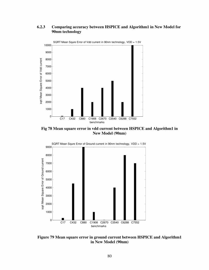
6.2.3 Comparing accuracy between HSPICE and Algorithm1 in New Model for
90nm technology
C17 C432 C880 C1908 C2670 C3540 C6288 C75520
1000
2000
3000
4000
5000
6000
7000
8000
9000
10000
benchmarks
sqrt
Mean S
quare
Err
or
of
Vdd c
urr
ent
SQRT Mean Squre Error of Vdd current in 90nm technology, VDD = 1.5V
Fig 78 Mean square error in vdd current between HSPICE and Algorithm1 in
New Model (90nm)
C17 C432 C880 C1908 C2670 C3540 C6288 C75520
1000
2000
3000
4000
5000
6000
7000
8000
9000
benchmarks
sqrt
Mean S
quare
Err
or
of
Gro
und c
urr
ent
SQRT Mean Squre Error of Ground current in 90nm technology, VDD = 1.5V
Figure 79 Mean square error in ground current between HSPICE and Algorithm1
in New Model (90nm)

81
6.2.4 Comparing accuracy between HSPICE and Algorithm2 in New Model for
90nm technology
C17 C432 C880 C1908 C2670 C3540 C6288 C75520
1000
2000
3000
4000
5000
6000
7000
8000
9000
10000
benchmarks
sqrt
Mean S
quare
Err
or
of
Vdd c
urr
ent
SQRT Mean Squre Error of Vdd current in 90nm technology, VDD = 1.5V
Figure 80 Mean square error in vdd current between HSPICE and Algorithm 2 in
New Model (90nm)
C17 C432 C880 C1908 C2670 C3540 C6288 C75520
2000
4000
6000
8000
10000
12000
14000
benchmarks
sqrt
Mean S
quare
Err
or
of
Gro
und c
urr
ent
SQRT Mean Squre Error of Ground current in 90nm technology, VDD = 1.5V
Figure 81 Mean square error in ground current between HSPICE and Algorithm 2
in New Model (90nm)

82
6.2.5 Comparing accuracy between HSPICE and Algorithm2 in New Model for
65nm technology
C17 C432 C880 C1908 C2670 C3540 C6288 C75520
1000
2000
3000
4000
5000
6000
7000
8000
9000
10000
benchmarks
sqrt
Mean S
quare
Err
or
of
Vdd c
urr
ent
SQRT Mean Squre Error of Vdd current in 65nm technology, VDD = 1.5V
Figure 82 Mean square error in vdd current between HSPICE and Algorithm 2 in
New Model (65nm)
C17 C432 C880 C1908 C2670 C3540 C6288 C75520
0.5
1
1.5
2
2.5
3x 10
4
benchmarks
sqrt
Mean S
quare
Err
or
of
Vdd c
urr
ent
SQRT Mean Squre Error of Vdd current in 65nm technology, VDD = 1.5V
Figure 83 Mean square error in ground current between HSPICE and Algorithm 2
in New Model (65nm)

83
6.3 Future work
Initially, this research project was started to see whether a simplified approach
of modeling switching current works or not. Now that it has been shown that the
approach works well, it can be extended. This work was based on a 2-input NAND gate.
One can explore it for more than 2 input NAND gates. Further, one can do it for all
other gate types. Secondly, in our proposed current model, simplified delay model has
been used. One can work on that to improve it further. Thirdly, the case when both
inputs switch and output does not switch in a 2 input NAND gate is not modeled in this
work. So, one can model that as well. Lastly, one can write a faster algorithm to reduce
computation time even further.

84
BIBLIOGRAPHY
[1] Sandip Kundu, Yi-Shing Chang, Chandra Trimurti, “a compact model for switching
current waveform of CMOS gates”
[2] Yi-Min Jiang, Angela Krystic, Kwang-Ting (Tim) Chang, “Estimation for Maximum
Instantaneous current through supply lines for CMOS circuits,” IEEE Transactions on
VLSI systems, Feb 2000.
[3] Harish Kriplani, Farid Najm, Ibrahim Hajj, “Maximum current estimation in CMOS
circuits,” 29th ACM/IEEE Design Automation Conference, 1992
[4] Anantha Chandrakasan, Jan M. Rabae, Borivoje Nikolic, “Digital Integrated circuits, a
design perspective,” 2nd
edition, Peason Education, Inc. 2003
[5] Lavagno, Martin, and Scheffer, “A survey of the field of electronic design
automation,” Electronic Design Automation for Integrated Circuits Handbook,
Taylor and Francis. 2006
[6] David Blaauw, Sanjay Pant, Rajat Chaudhry, Rajendran Panda, “Design and
Analysis of Power Supply Networks,” chapter 20, vol II, Electronic Design
Automation for Integrated Circuits Handbook, Taylor and Francis. 2006
[7] Howard H. Chen, David D. Ling, “Power Supply noise analysis methodology for deep-
submicron VLSI chip design,” Design Automation Conference, Anaheim, CA 1997
[8] A. Chatzigeorgiou, S. Nikolaidis, “Efficient output waveform evaluation of a CMOS
inverter based on short-circuit current prediction,” John Wiley and Sons, Ltd, 2002
[9] Hedenstierna N, Jeppson KO,”CMOS circuit speed and buffer optimization,” IEEE
Transactions on Computer-Aided Design CAD-6(2):270 –281, 1987
[10] Hirata A, Onodera H, Tamaru K, “Estimation of short-circuit power dissipation for
static CMOS gates,” IEICE Transactions on Fundamentals, E79-A(3):304–311, 1996
[11] Bisdounis L, Nikolaidis S, Koufopavlou O, “Analytical transient response and
propagation delay evaluation of the CMOS inverter for short-channel devices,” IEEE
Journal of Solid-State Circuits, 33(2):302– 306, 1998
[12] Sakurai T, Newton AR.,” Alpha-power law MOSFET model and its applications to
CMOS inverter delay and other formulas,” IEEE Journal of Solid-State Circuits
5(2):584– 594, 1990
[13] Chatzigeorgiou A, Nikolaidis S, Tsoukalas I, ”A modeling technique for CMOS gates,”
IEEE Transactions on Computer-Aided Design of Integrated Circuits and Systems,
18(5):557– 575, 1999
[14] Kong J-T, Hussain SZ, Overhauser D, “Performance estimation of complex MOS
gates,” IEEE Transactions on Circuits and Systems—I: Fundamental Theory and
Applications 44(9):785 –795, 1997

85
[15] A. Nabavi-Lishi and N.C. Rumin, ”Inverter models of CMOS gates for supply current
and delay evaluation,” IEEE Transactions on Computer Aided Design, 13(10):1271-
1279, 1994
[16] Y.-H. Jun, K. Jun, and S.-B. Park, “An accurate and efficient delay time modeling for
MOS logic circuits using polynomial approximation,” IEEE Transactions on Computer
Aided Design, 8(9):1027{1032, 1989.
[17] Qi Wang and Sarma B.K. Vrudhula, “A new short circuit power model for complex
CMOS gates,” Low power design proceeding, 1999
[18] F. Rouatbi, B. Haroun, and A. J. Al-Khalili, “Power estimation tool for sub-micron
CMOS VLSI circuits,” in Proceedings of IEEE/ACM International Conference on
Computer-Aided Design, pp 204-209, Santa Clara, CA, November 8-12, 1992.
[19] U. Jagau, “ SIMCURRENT- an efficient program for the estimation of the current flow
Of complex CMOS circuits, “ in Proceedings of IEEE International Conference on
Computer-Aided Design, pp. 396-399, Santa Clara, CA, November 11-15, 1990.
[20] A.-C. Deng, Y.-C. Shiau, and K.-H. Loh, “Time domain current waveform simulation of
CMOS circuits,” in Proceedings of IEEE International Conference on Computer-Aided
Design, pp. 208-211, Santa Clara, CA, November 7-10, 1988.
[21] S. Chowdhury and J. S. Barkatullah, “Estimation of maximum currents in MOS IC logic
circuits,” IEEE Transactions on Computer-Aided Design, vol. 9, no. 6, pp. 642-654, June
1990.
[22] S. Devadas, K. Keutzer, and J. White, “Estimation of power dissipation in CMOS combi-
national circuits using Boolean function manipulation,” IEEE Transactions on
Computer-Aided Design, no. 3, pp. 373-383, March 1992.
[23] Anas A. Hamoui, Nicholas Rumin, “An analytical model for current, delay and power
analysis of submicron CMOS logic circuits,” IEEE Transactions of circuits and systems –
II, 2000
[24] A. Nabavi-Lishi and N. Rumin, “Delay and bus current evaluation in CMOS logic cir-
cuits,” Proceedings of IEEE/ACM International Conference on Computer-Aided
Design, pp. 198-203, Santa Clara, CA, November 8-12, 1992.