Embed Size (px)
Citation preview

STMicroelectronics
Interconnect impact on circuit performances in Deep Sub-Micron
technologies
Cristiano ForzanCentral R&D – NVM Design Platform
Bologna, June 2004

NVM Design Platform – Cristiano Forzan
Outline
CMOS device and interconnect scaling overview
Introduction to Static Timing Analysis
Interconnect resistance effects
References

NVM Design Platform – Cristiano Forzan
CMOS technology scaling overview
800 KTx800 KTx
1µm technology (1990)
1mm
0.13µm technology (2001)
1cm

NVM Design Platform – Cristiano Forzan
Ideal CMOS scaling
wiring
gate
drainsourcen+ n+
p-substratedoping NA
Vdd
L
W
tox
xd SVdd, Vth
1/SNA
SW, L, tox
Ideal Scaling Factor
ScaledParameter

NVM Design Platform – Cristiano Forzan
Interconnect reverse scaling
1/S1/SCurrent density1/S31RC delay
11Capacitance1/S21/S2Resistance
1/sqrt(S)SWireLengthSSILD ThicknessSSWire ThicknessSSLinewidth & Spacing
Global WiringLocal Wiring
NVM Design Platform – Cristiano Forzan
DSM scaling impact on delay
0.1
10
100
Rel
ativ
e D
elay
Process Technology Node [nm]180 130 100 70 50 35
Global NetLocal NetGate
(from ITRS 99)
Gate delay scalesLocal interconnect
delay scalesGlobal interconnect
delay dominates– Global interconnects
do not scale with feature sizes

NVM Design Platform – Cristiano Forzan
Quasi-ideal interconnect scaling
0.5 µm technology 0.25 µm technology
ideal quasi-ideal
Keeping wire resistance low– Increase the wire aspect ratio (AR = height / width)– Use copper instead of aluminium

NVM Design Platform – Cristiano Forzan
Interconnect capacitances
Substrate
Metal 1
Metal 2
CFRINGE CAREA
CCROSSOVER
CCOUPLING

NVM Design Platform – Cristiano Forzan
Interconnect capacitance trends
0
1
2
3
4
0.050.10.150.20.250.30.350
20
40
60
80
100 Aspect Ratio Pitch (um)Cc/Ctotal (%)
Technology Generation (µm)C
coup
ling
/ Cto
tal(
%)
Asp
ect R
atio
, P
itch
(µm
)Interconnect average length and routing density increase
Wire aspect ratio increases
Coupling capacitance dominates over ground capacitance
Interconnect capacitance dominates gate capacitance

NVM Design Platform – Cristiano Forzan
Traditional top-down design flowRTL description
Any top-down flow requires some predictive capabilities
Traditional top-down flows are effective when performances can be predicted with the wireload model
Logic Synthesis
Placement
Routing
Polygon implementation

NVM Design Platform – Cristiano Forzan
Interconnect impact on design flowRTL description
Polygon implementation
Logic Synthesis
Placement
Routing
The evolutionary response to the DSM problem has been a stronger integrationbetween the synthesis and the place&route process
This is what Physical Synthesis does today
Revolutionary breakthrough?

NVM Design Platform – Cristiano Forzan
Outline
CMOS device and interconnect scaling overview
Introduction to Static Timing Analysis– Timing verification– Delay calculation– Constraints
Interconnect resistance effects
References

NVM Design Platform – Cristiano Forzan
Dynamic Timing Simulation
Advantages
– Can check asynchronous interfaces
– No need to specify false and multicycle paths, clock model, etc
– Can be very accurate (SPICE)
Disadvantages
– Analysis quality depends on stimulus vectors
– Non-exhaustive – virtually impossible to check every path
– Long run times

NVM Design Platform – Cristiano Forzan
Static Timing Simulation
Advantages
– Fast – design is analyzed in one pass, for one clock cycle
– Exhaustive – checks all topological paths in design
– Does not require verification environment
Disadvantages
– Less accurate– Must define timing
requirements / exceptions– Difficulty handling
asynchronous designs, false paths

NVM Design Platform – Cristiano Forzan
Principles of Static Timing Verification
Netlist is represented as DAG – Directed Acyclic GraphDelay values associated with nodes (Cells) and links (Nets)Total path delay is the sum of Path delay values
2
3
24
1
11
11
In
Out11

NVM Design Platform – Cristiano Forzan
Path-based STA
Timing information is associated with topological paths– First, extract all possible topological paths– Next, for each path calculates its delay and compare it
with endpoint (required) value
Path-based:2+2+3 = 7 (OK)2+3+1+3 = 9 (OK)2+3+3+2 = 10 (OK)5+1+1+3 = 10 (OK)5+1+3+2 = 11 (Problem!)5+1+2 = 8 (OK)
31
31
21
32
AT=2
AT=5
RAT=10
NVM Design Platform – Cristiano Forzan
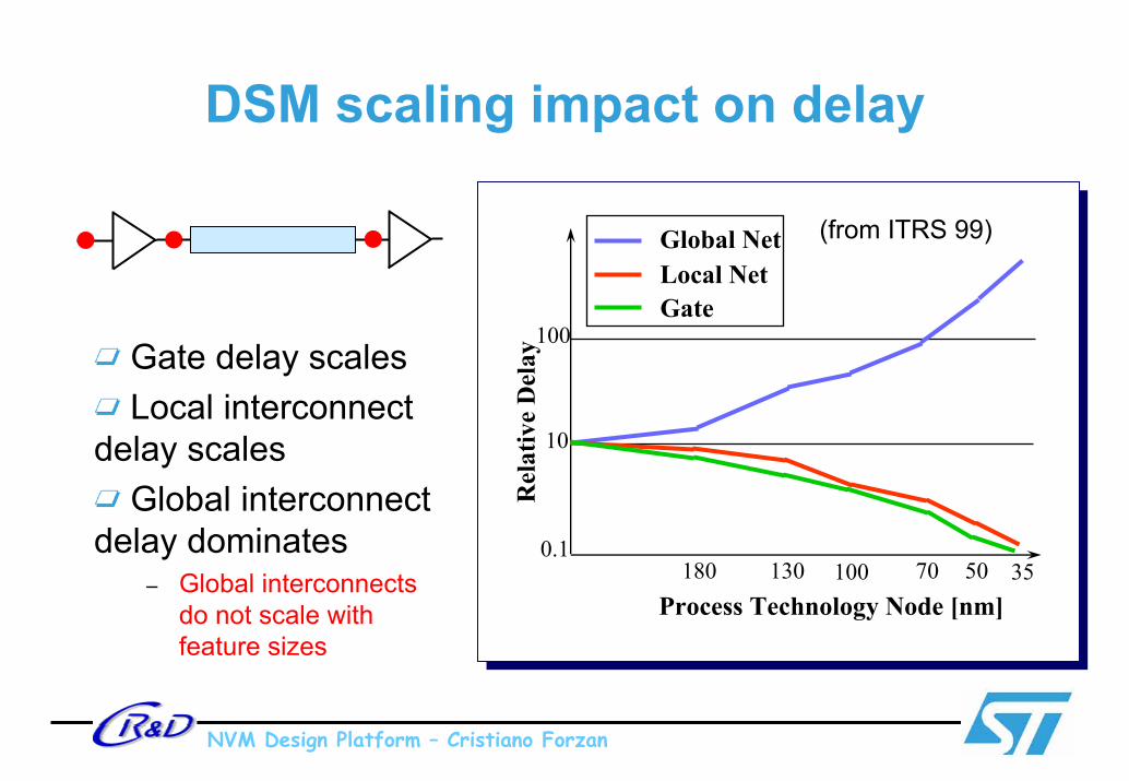
Timing Paths TypesFour types of Timing Paths
Input to Register (Synchronous)Register to Register (Synchronous)Register to Output (Synchronous)Input to Output (Asynchronous)
Each path has:StartPoint (Input port or FF output)EndPoint (Output port or FF input)Calculated value for path delay
In Out
In Out

NVM Design Platform – Cristiano Forzan
Outline
CMOS device and interconnect scaling overview
Introduction to Static Timing Analysis– Timing verification– Delay calculation– Constraints
Interconnect resistance effects
References

NVM Design Platform – Cristiano Forzan
Path delay calculation
The actual path delay is the sum of the Net and the Cell delays along the timing path– Net Delay – total time for charging/discharging all the
parasitics of a given net. It is a function of:Net capacitanceNet resistance
– Cell Delay – delay arc between corresponding input and output ports of the cell. It is a function of:
Input transition time (Slew)Total output load Process parameters (Temperature, Power supply)

NVM Design Platform – Cristiano Forzan
Net Delay Calculation (PreLayout)
Wire Load Model– Net length is a function of net fanout and chip area– For a given area, averages of R and C are estimated
for different fanouts– Net delay is calculated simply as R * C
0.0463
0.0302
0.0151
0.0203
0.0162
0.0121
Resistance as a function of fanout :
Capacitance as a function of fanout : For fanout = 3
Net delay = 0.046 * 0.020

NVM Design Platform – Cristiano Forzan
Cell Delay Calculation
Temperature,Power Level,Process
Cell delay is a function of– Input Transition Time (calculated by previous gate)– Total Output Capacitance (Net cap + sum of attached
Pin Caps)– Operating Conditions

NVM Design Platform – Cristiano Forzan
Cell Delay and Slew Calculation
Delay is calculated using 2-Dimensional Nonlinear Delay Model. Main calculation part is interpolation between nearest table values:
Total Cload (fF)
1310850.1
764.530
0.50.40.30.2
InputTransition
(ns)
A similar model is used for the Cell Slew calculationAfter calculation, delay is scaled by the operating conditions:
– Final_delay = Table_delay * Kvoltage * Ktemp * Kprocess

NVM Design Platform – Cristiano Forzan
Types of Cell Timing ArcsCombinatorial Cells: from all inputs to output:
A
B
C
Y
Sequential Cells: from Clock Input to outputs (propagation delay) and from Clock Input to Data Input (setup, hold checks):
D
Clk
Qn
Q

NVM Design Platform – Cristiano Forzan
Outline
CMOS device and interconnect scaling overview
Introduction to Static Timing Analysis– Timing verification– Delay calculation– Constraints
Interconnect resistance effects
References

NVM Design Platform – Cristiano Forzan
Path Constraints Types
Main path constraints include:Setup time (Input-to-Reg and Reg-to-Reg paths)Hold time (Input-to-Reg and Reg-to-Reg paths)Input delay (Input-to-Reg and Input-to-Output paths)Output delay (Reg-to-Output and Input-to-Output paths)
In
In
Out
Out
Clk
NVM Design Platform – Cristiano Forzan
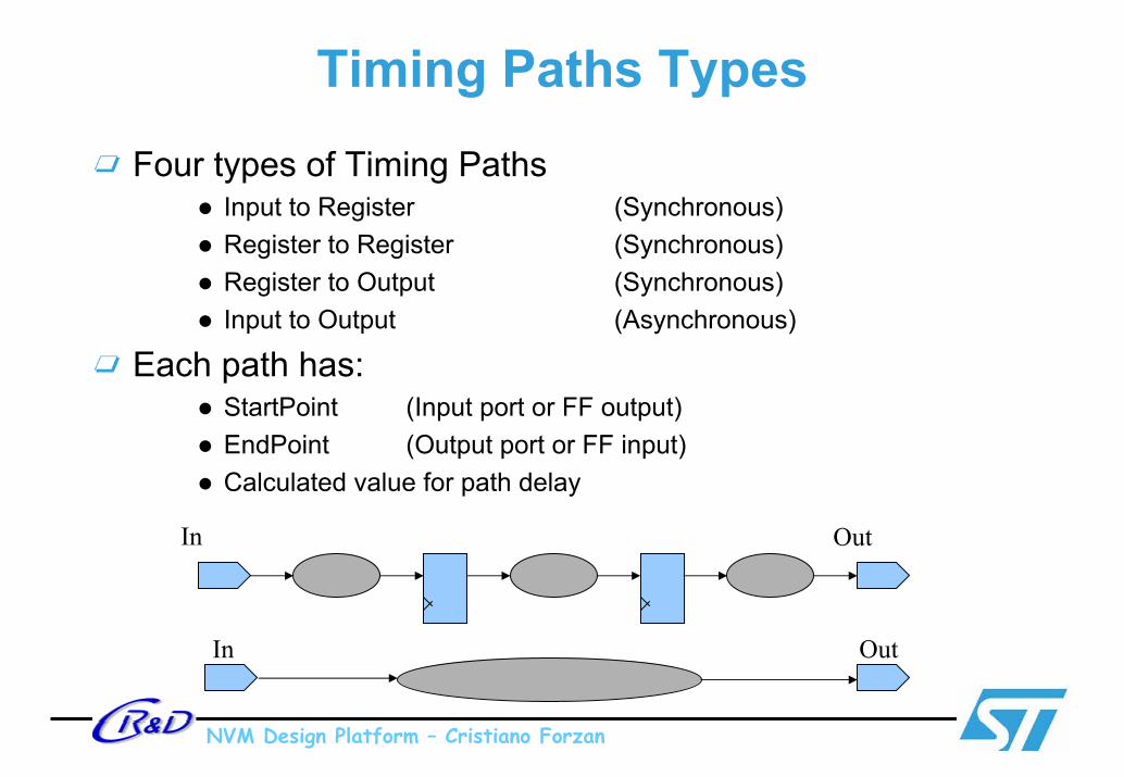
Setup and Hold Times
Setup: amount of time data must be stable at the data pin of FF before the clock capturing edgeHold: amount of time data must remain stable at the data pin of FF after the clock capturing edge
Clk
In D Hold Check refers to the sameclock edge:TD – TCLK > THold
Setup Check refers to the nextClock edge (add clock period) :(TCLK + TPeriod) – TD > TSetup
Hold Setup
Clk
D

NVM Design Platform – Cristiano Forzan
Other constraints: Design Rules Check
Design Rules are electrical checks performed on each gate. They are defined in the technology libraryChecking min and max limits for:
Net / Port capacitanceNet Transition timesNet fanout
Max capacitance example:
max_capacitanceattribute fromTechnology library
Total capacitiveload includes pin load and netcapacitance

NVM Design Platform – Cristiano Forzan
Outline
CMOS device and interconnect scaling overview
Introduction to Static Timing Analysis
Interconnect resistance effects
References

NVM Design Platform – Cristiano Forzan
Interconnect resistance impact
For DSM technologies (0.25µm and below) RC distributed effects become dominant
Many iterations and no guarantee to achieve timing closure
For technologies up to 0.35µmdelay estimation based on the wireload model can be accurate
Few iterations for timing closure

NVM Design Platform – Cristiano Forzan
Wire resistance impact on delay
A Z R
Tstage(A-R) = Tgate(A-Z) + Twire(Z-R)
f(TIN, CZ)

NVM Design Platform – Cristiano Forzan
Effective capacitance
A Z
Ceffective
Tp
Tp1
The propagation time across the gate decreases due to the shielding resistance effect
The effective capacitance concept is introduced

NVM Design Platform – Cristiano Forzan
Interconnect delay estimation
The driving cell can be represented by a Thevenin equivalent model
The output waveform can be obtained via convolution of the driving point voltage waveform with the transfer function HZR
SPICE: generally too much expensive
A Z R

NVM Design Platform – Cristiano Forzan
Elmore delay
τ
Vin
t R1 R2 R3 R4 R5
R6 R7
C1 C2 C3 C4 C5
C6 C7
Vin( ) dtthtTD ∫∞
=0
It is an upper bound on the delay of an RC tree response: T τ≥D

NVM Design Platform – Cristiano Forzan
Elmore delay calculation
+= 115 CRTD
++ 221 )( CRR+++ 3321 )( CRRR
++++ 44321 )( CRRRR
+++++ 554321 )( CRRRRR
+61CR
71CR
R1 R2 R3 R4 R5
R6 R7
C1 C2 C3 C4 C5
C6 C7
Vin
∑=
=N
kkikD CRT
i1
54321
6 7
Elmore delay can be calculated very efficiently– Linear time w.r.t the RC tree size
NVM Design Platform – Cristiano Forzan
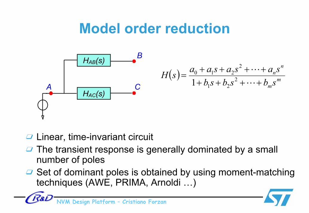
Model order reduction
A C
BHAB(s)
HAC(s)
( ) mm
nn
sbsbsbsasasaasH
++++++++
=L
L2
21
2210
1
Linear, time-invariant circuitThe transient response is generally dominated by a small number of polesSet of dominant poles is obtained by using moment-matching techniques (AWE, PRIMA, Arnoldi …)

NVM Design Platform – Cristiano Forzan
Moment matching technique (I)The goal of model order reduction techniques is to obtain a set of qapproximate dominant poles efficiently:
( ) mqps
kps
kps
ksHq
q <<−
++−
+−
= ,2
2
1
1* L
( ) tpq
tptp qekekekth +++= L2121
*
The i-th moment of the function f(t) is defined as:
( ) ( )dttfti
m ii
i ∫∞−
=0!
1
112
21
1
1*+++ +++= i
q
qiii
pk
pk
pkm L

NVM Design Platform – Cristiano Forzan
Moment matching technique (II)
The moments of H*(S) are forced to match the actual circuit moments:
1222
22
1
1 mpk
pk
pk
q
q =+++ L
02
2
1
1 mpk
pk
pk
q
q =+++ L
…
12222
22
1
1−=+++ qq
q
qqq m
pk
pk
pk
L

NVM Design Platform – Cristiano Forzan
Moment matching technique (III)Once the reduced order model is obtained, the output waveform iscalculated via convolution with the input signal.
– Example: saturated ramp
( ) ( ))(1 0)(
12
01
0 ttpepr
ttVtv k
ttpq
k k
kDDZ
k −−−−
= −
=∑
10 ttt ≤≤For time interval
t0 t1
VDD
A H*(s)Z
1tt ≥For time interval
( ) ( ))( 01)()(
12
01
10 ttpeepr
ttVtv k
ttpttpq
k k
kDDZ
kk −−−−
= −−
=∑

NVM Design Platform – Cristiano Forzan
Asymptotic Waveform Evaluation
A linear time-invariant network can be represented by the state equation:
BuAxx +=&
In the frequency domain:
( ) ( ) ( )sBUsAXxssX +=− )0(
The network transfer function is expressed by:
( ) ( )( ) ( ) BAsIsUsXsH 1−−==

NVM Design Platform – Cristiano Forzan
Asymptotic Waveform Evaluation (II)The transfer function is the Laplace transform of the impulse response:
( ) ∫∞
−=0
)( dtthesH st
The coefficients of the MacLaurin series expansion are the moments of the impulse response
( ) ( )∫ ∑∑∞ ∞
=
∞
=
=−
=0 00
)(!1
kk
kk
k
kk msdttht
kssH
From the previous representation:( ) BsAsAIABAsIsH )()( 22111 L+++−=−= −−−−

NVM Design Platform – Cristiano Forzan
Moment determination
The moments are computed recursively
BAm 10
−=
012
1 mABAm −− ==
11)1(
−−+− == q
qq mABAm
State matrix is inverted only once

NVM Design Platform – Cristiano Forzan
Moment computation for RC treesNodal Analysis instead of State Analysis
– Based on KCL and KVL– It is not a general methodology but it is easier than State Equation
Nodal Analysis formulation:
BuCGvCv 11 −− +=&
u is a unit step input voltageC is the diagonal capacitance matrixG is the conductance matrix

NVM Design Platform – Cristiano Forzan
Nodal AnalysisFirst moments generation
Replace input drivers with their final valuePerform dc analysisMoments are the voltages across the capacitors R1 R2
R3
u(t)
L1
L3
L2
C3 C4
C1 C2Successive momentsSet input drivers to zeroReplace each capacitor with a current source I=mk-1C (V= mk-1L)Perform dc analysisMoments are the voltagesacross the current sources
mL1L1
mL3L3
mL2L2
mC3C3
mC1C1 mC2C2
mC4C4
NVM Design Platform – Cristiano Forzan
Outline
CMOS device and interconnect scaling overview
Introduction to Static Timing Analysis
Interconnect resistance effects
References

NVM Design Platform – Cristiano Forzan
References (I)H.B. Bakoglu “Circuits, Interconnects and Packaging for VLSI”, Addison-Wesley, 1990.N. Weste, K. Eshraghian “Principles of CMOS VLSI Design”, Addison-Wesley, 1993.
D. Sylvester, C. Hu “Analytical Modeling and Characterization of Deep-Submicrometer Interconnect” Proc IEEE, Vol 89 No 5 May 2001D. Sylvester, K. Keutzer “Getting to the Bottom of Deep Submicron” Proc ICCAD, 1998A. Vittal, M. Marek-Sadowska “Crosstalk reduction for VLSI”, IEEE Trans. on CAD, 1997.F. Dartu, L.T. Pileggi “Calculating worst-case gate delays due to dominant capacitance coupling” Proc. DAC 1997.W.C. Elmore “The transient analysis of damped linear networks with particularregard to wideband amplifiers”, J. Appl. Phys, Vol 19 No 1 1948

NVM Design Platform – Cristiano Forzan
References (II)
L. Pillage, R. Rohrer “Asymptotic Waveform Evaluation for timing analysis”, IEEE Trans. on CAD 1990A. Odabasioglu, M. Celik, L. T. Pileggi “PRIMA: Passive Reduced-Order Interconnect Macromodeling Algorithm”, 34th DAC 1997K. L. Shepard, Z. Tian “Return-Limited Inductances: A Practical Approach to On-Chip Inductances Extraction”, IEEE Trans. on CAD Vol 19 No 4 2000.Y. I. Ismail, E. G. Friedman, J. L. Neves “Figures of Merit to Characterize the Importance of On-Chip Inductance”, IEEE Trans. on VLSI Systems Vol 7 No 4 1999

NVM Design Platform – Cristiano Forzan
Our works on this field (I)
C. Forzan, B. Franzini and C. Guardiani “Accurate and Efficient Macromodel of Submicron Digital Standard Cells”, DAC 1997
D. Pandini, C. Guardiani, P. Gubian “A Moment Matching BasedMethodology for Crosstalk Analysis”, ASIC 1997
D. Pandini, P. Scandolara, C. Guardiani “Network Reduction for Crosstalk Analysis in Deep Submicron Technologies”, TAU 1997
D. Pandini, P. Scandolara, C. Guardiani “Reduced order macromodel of coupled interconnects for timing and functional verification of sub half-micron IC designs”, Asia and Pacific DAC 1997

NVM Design Platform – Cristiano Forzan
Our works on this field (II)
B. Franzini, C. Forzan, D. Pandini, Y. Liu and C. Guardiani “NonlinearMacromodels of Large Coupled Interconnect Networks”, CICC 1998
C. Guardiani, C. Forzan, B. Franzini, D. Pandini “Modeling the Effectof Wire Resistance in Deep Submicron Coupled Interconnects forAccurate Crosstalk Based Net Sorting”, PATMOS 1998
B. Franzini, C. Forzan, D. Pandini, P. Scandolara, A. Dal Fabbro“Crosstalk Aware Static Timing Analysis: a Two Step Approach”, ISQED 2000
B. Franzini, C. Forzan “Crosstalk Aware Static Timing Analysis Environment”, ESNUG 2001