Embed Size (px)
Citation preview

Effects of Global Interconnect Optimizations on
Performance Estimation of Deep Sub-Micron Design
Yu (Kevin) Cao1, Chenming Hu1, Xuejue Huang1,
Andrew B. Kahng2, Sudhakar Muddu3,
Dirk Stroobandt4, Dennis Sylvester5
1EECS Department, University of California, Berkeley2Now with ECE and CS Department, University of California, San Diego
3Formerly with Silicon Graphics, Inc. 4ELIS Department, Ghent University, Belgium
5Now with EECS Department, University of Michigan, Ann Arbor

11/06/2000 2
Outline
Introduction
Study implementation
Global interconnect optimization issues Inductance effect
Repeater insertion
Via parasitics
Conclusions

11/06/2000 3
Performance Prediction
Performance estimated from critical path analysis Previous prediction assumes:
RC line model for interconnect delay Switch factor bounded by {0,2} Optimal repeater sizing and ideal placement Design constraints excluded, such as noise margin, delay
uncertainty and area cost Via resistance from buffer insertion neglected
How valid are these assumptions?
Critical Path Delay Estimation
11/06/2000 4
Research Framework
GSRC Technology Extrapolation (GTX) Engine :
http://vlsicad.cs.ucla.edu/GSRC/GTX Allows users to flexibly capture and study the impact of
alternative modeling choices and optimization constraints

11/06/2000 5
Simulation Setup
Typical 0.18μm MOSFET technology 15mm copper global interconnect, line thickness=1.3μm Inverting buffers inserted
Variables TargetsLine width and spacingShield configurationBuffer sizeBuffer placement
Line delayPeak noiseDelay uncertainty: best and
worst delay when noise exists

11/06/2000 6
Line Inductance
In DSM regime, inductance is more important with Increasing operation frequency Lower line resistance
• Larger global interconnect cross-sectional dimension
• using Cu
Vin
Vdd
Vout RC
Vdd
Vout RLC

11/06/2000 7
Inductance Effect on Line Delay
Line behavior is RLC dominant when b12-4b2<0,
where b1=RsC+RsCL+RCL, b2=RsC2/6+RsRCCL/2+RC2/24+R2CCL/6+LC+LCL
Simple RC model underestimates line delay by more than 40% in RLC-dominated cases
25
50
75
100
125
150
175
200
225
3 4 5 6 7 8 9 10Interconnect Length (mm)
Inte
rco
nn
ect
Del
ay (
ps)
RC_Bakoglu
RLC_Friedman
RLC_Kahng/Muddu
HSPICE
RLC-dominated Case

11/06/2000 8
Switch Factor (SF) Effect
Previous models simply use switch factor bounded by {0,2} for further simulations
Detailed analysis predicts that the range of SF can be {-1,3}, depending on different transition time of inputs*
*A.B. Kahng, S. Muddu, and E. Sarto, “On Switch Factor Based Analysis of Coupled RC Interconnects”, Proc. ACM/IEEE Design Automation Conf., June 2000, pp. 79-84
SF*Cc
Cc
Vin1
Vin2

11/06/2000 9
Shielding Technology
Shielding is helpful to define the current return path for inductance coupling and to reduce crosstalk noise. But it increases area cost for signal lines
Cost function = Signal wire pitch x Repeater size x Number of repeaters
No Shielding (NS)
One Side Shielding (1S)
Two Side Shielding (2S)
Vdd/GND LinesSignal Lines

11/06/2000 10
Shielding Cost Optimization
Cost optimization constraints: line delay < 1ns; noise peak < 20% Vdd; transition time < 500ps; delay uncertainty < 15%
Ignoring inductance can overestimate cost function (>20%)
2
4
6
8
10O
pti
miz
ed C
ost
wit
hin
Co
nst
rain
ts
NS 1S 2S
RC/SF=1
RC/SF=2
RC/SF=3
RLC/SF=1
RLC/SF=2
RLC/SF=3
11/06/2000 11
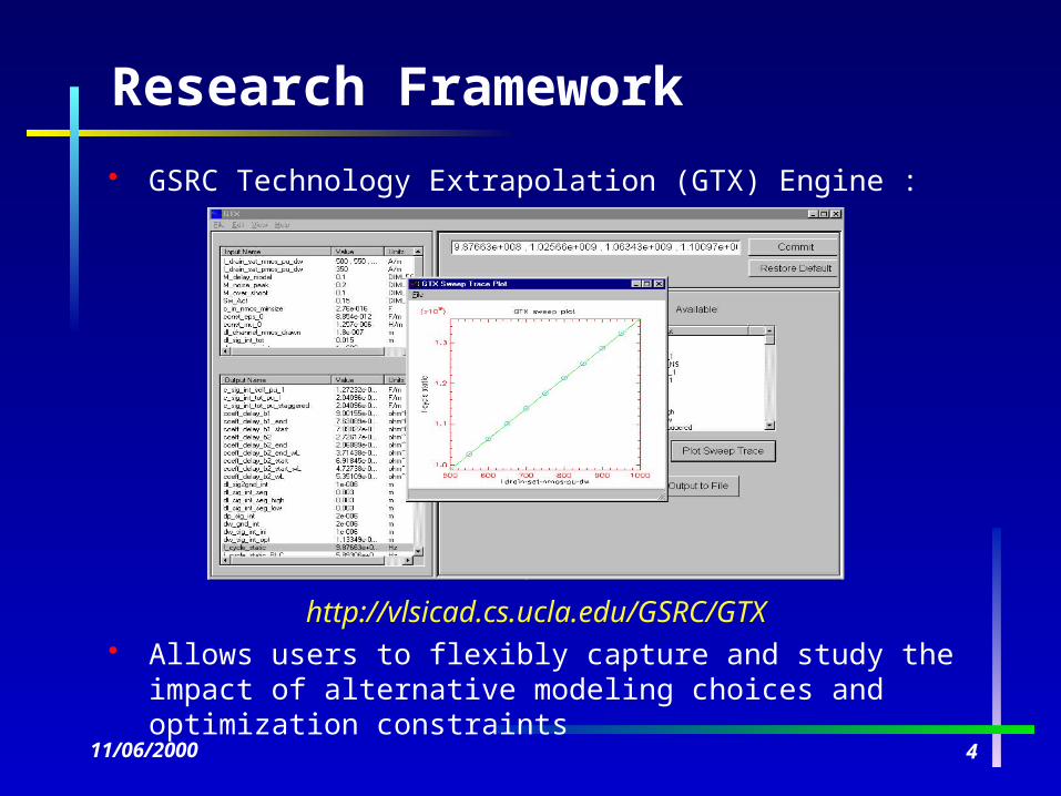
Wire and Repeater Sizing
For a line with fixed length, its width and spacing need to be well sized to optimize delay
Non-linear dependence of line delay on line length enables suitable buffer insertion to improve performance
Buffer scaled based on the loading it drives
Critical Path Structure
11/06/2000 12
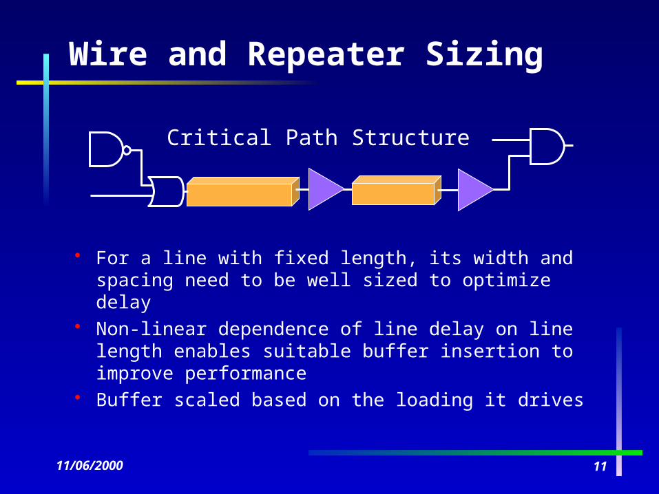
Wire Size Optimization
RC formula for optimal line width: *
RC formula overestimates optimal width up to 30% from RLC model *J. Cong and D.Z. Pan, “Interconnect Estimation and Planning for Deep Submicron
Designs”, Proc. DAC, 1999, pp. 507-510
aD
Lfinopt CR
ClCRlW
2
2
0 2 4 6 8 10
0.4
0.6
0.8
1.0
1.2
1.4
1.6
1.8
2.0
2.2
0.4
0.6
0.8
1.0
1.2
1.4
1.6
1.8
2.0
2.2
Repeater size = 100 X min
Formula RC, 1 pole
Op
tim
al W
ire
Wid
th (
μm
)
Line Length (mm)
RLC

11/06/2000 13
Repeater Size Optimization
Bakoglu sizing:
Simple sizing expression overestimates optimal repeater size by 400%
0 100 200 300 400 500
0.8
1.0
1.2
1.4
1.6
1.8
2.0
2.2
2.4
Bakoglu optimal sizing
Lsegment = 2.14 mm
W=S=1.0 m W=S=0.5 m
Cri
tica
l Pat
h D
elay
(n
s)
Repeater Size (X min size)
1
2
3
4
5
6
No
rmalized
En
ergy-D
elay Pro
du
ct
in
D
CR
CRS
int
int
11/06/2000 14
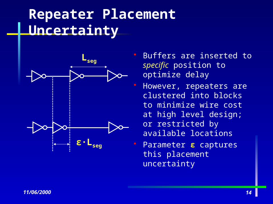
Repeater Placement Uncertainty
Buffers are inserted to specific position to optimize delay
However, repeaters are clustered into blocks to minimize wire cost at high level design; or restricted by available locations
Parameter ε captures this placement uncertainty
Lseg
ε·Lseg

11/06/2000 15
Impact of ε
Repeater placement uncertainty ε has a large impact on peak noise (up to >70%) but little impact on delay (<5%)
0.0 0.2 0.4 0.6 0.8 1.0
1.0
1.1
1.2
1.3
1.4
No
rmal
ized
Del
ay
Repeater Placement Uncertainty (
1.0
1.1
1.2
1.3
1.4
1.5
1.6
1.7
1.8 No
rmalized
Peak N
oise
SF = 1 SF = 2 SF = 3

11/06/2000 16
With inverting buffer, staggered repeater placement makes overall switch factor close to one*
Peak noise and delay uncertainty benefit from staggered insertion
*A. B. Kahng, S. Muddu, and E. Sarto, “Tuning Strategies for Global Interconnects in High-Performance Deep Submicron IC’s”, VLSI Design 10(1), 1999, pp. 21-34
Staggered Insertion of Repeaters
Normal Repeater Insertion
Staggered Repeater Insertion

11/06/2000 17
Non-staggered vs. Staggered
Staggered insertion significantly reduces peak noise to 4-7 times smaller than that of normal non-staggered insertion and almost eliminates delay uncertainty
Delay U
ncertain
ty Ratio
-0.5
-0.3
-0.1
0.1
0.3
0.5
0.7
0.9
1.1
0.00
0.05
0.10
0.15
0.20
0.25
0.30
0.35
0.40
0.4 0.6 0.8 1.0 1.2 1.4 1.6 1.8 2.0
Vp
eak
/Vd
d (%
)
Non-staggered
Staggered
Interconnect Spacing (μm)
SF=3
11/06/2000 18
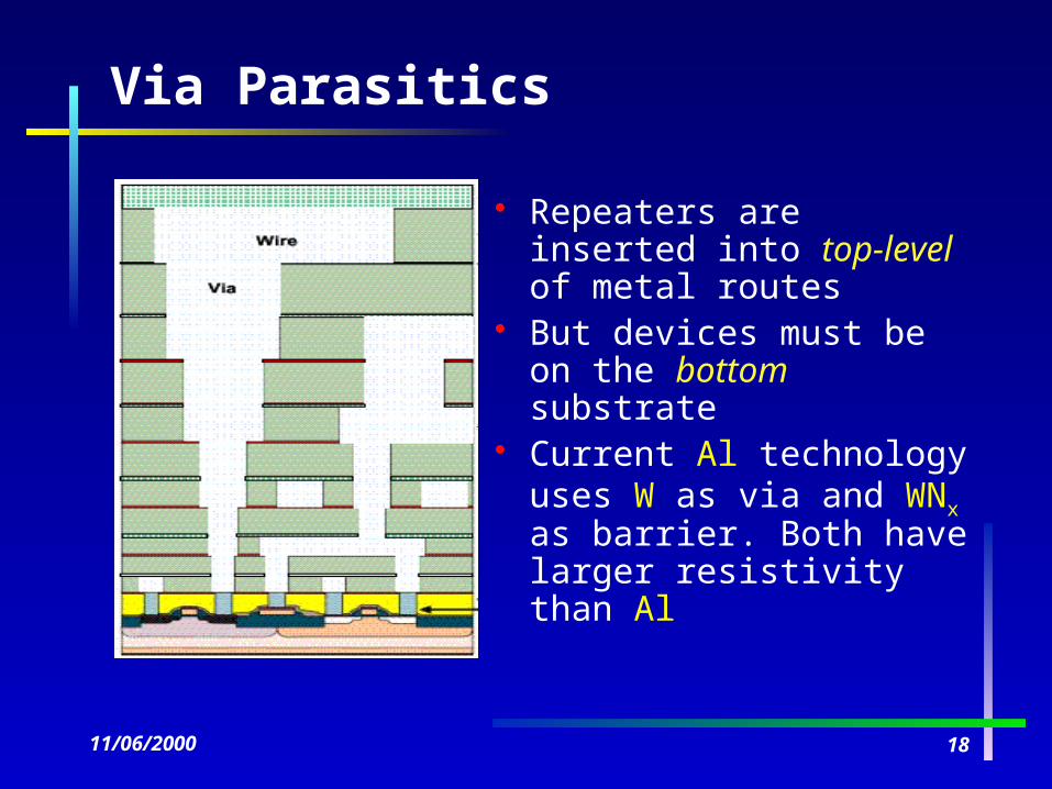
Via Parasitics
Repeaters are inserted into top-level of metal routes
But devices must be on the bottom substrate
Current Al technology uses W as via and WNx as barrier. Both have larger resistivity than Al

11/06/2000 19
Via Resistance Effect
Total via stack resistance is 47Ω for 0.18μm Al technology (signal line resistance is about 40Ω/mm)
Ignoring via parasitic resistance can introduce 10-20% underestimation of delay
In the future: copper can be used as via and may significantly reduce such impact
20 40 60 80 100 120 140 160
6
8
10
12
14
16
18
20
6
8
10
12
14
16
18
20
SF = 1 SF = -1
SF = 3
% In
crea
se in
pat
h d
elay
Repeater Size (X min size)

11/06/2000 20
Summary
Including Delay Noise DU Optimal Size
L + + + –ε + + + +
Staggered
Repeater x – – xRvia + x x +
+: previous models underestimate;
–: previous models overestimate;
x: no obvious change;

11/06/2000 21
Conclusions
Have quantified several large sources of error in standard models used for interconnect optimization Line inductance, via resistance Design techniques: shielding, repeater clustering
and repeater staggering Accurate analytical models are required for
optimal line and repeater sizing, and for accurate estimation of interconnect resource requirements
GTX allows rapid development, validation of interconnect performance models and optimizations