Embed Size (px)
Citation preview
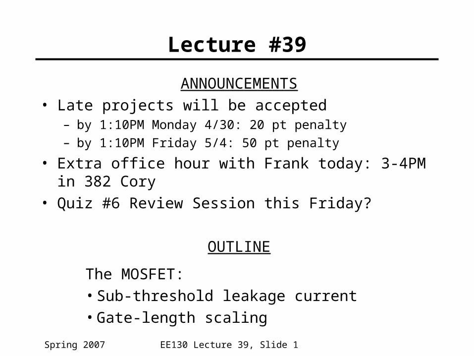
EE130 Lecture 39, Slide 1Spring 2007
Lecture #39
ANNOUNCEMENTS• Late projects will be accepted
– by 1:10PM Monday 4/30: 20 pt penalty– by 1:10PM Friday 5/4: 50 pt penalty
• Extra office hour with Frank today: 3-4PM in 382 Cory• Quiz #6 Review Session this Friday?
OUTLINE
The MOSFET:• Sub-threshold leakage current• Gate-length scaling
EE130 Lecture 39, Slide 2Spring 2007
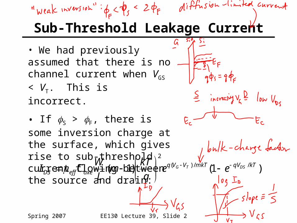
Sub-Threshold Leakage Current
• We had previously assumed that there is no channel current when VGS < VT. This is incorrect.
• If S > F, there is some inversion charge at the surface, which gives rise to sub-threshold current flowing between the source and drain:
)1()1( //)(
2
kTqVmkTVVqoxeeffDS
DSTG eeq
kTm
L
WCI
EE130 Lecture 39, Slide 3Spring 2007
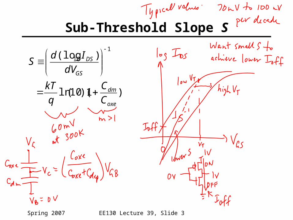
Sub-Threshold Slope S
)1)(10(ln
)(log1
10
oxe
dm
GS
DS
C
C
q
kT
dV
IdS
EE130 Lecture 39, Slide 4Spring 2007
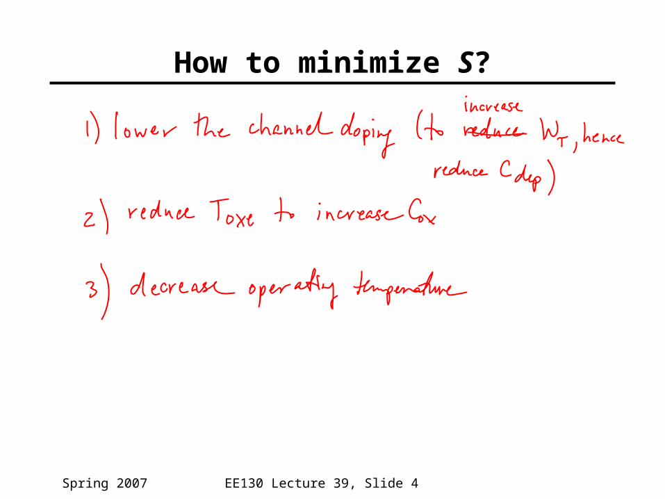
How to minimize S?
EE130 Lecture 39, Slide 5Spring 2007
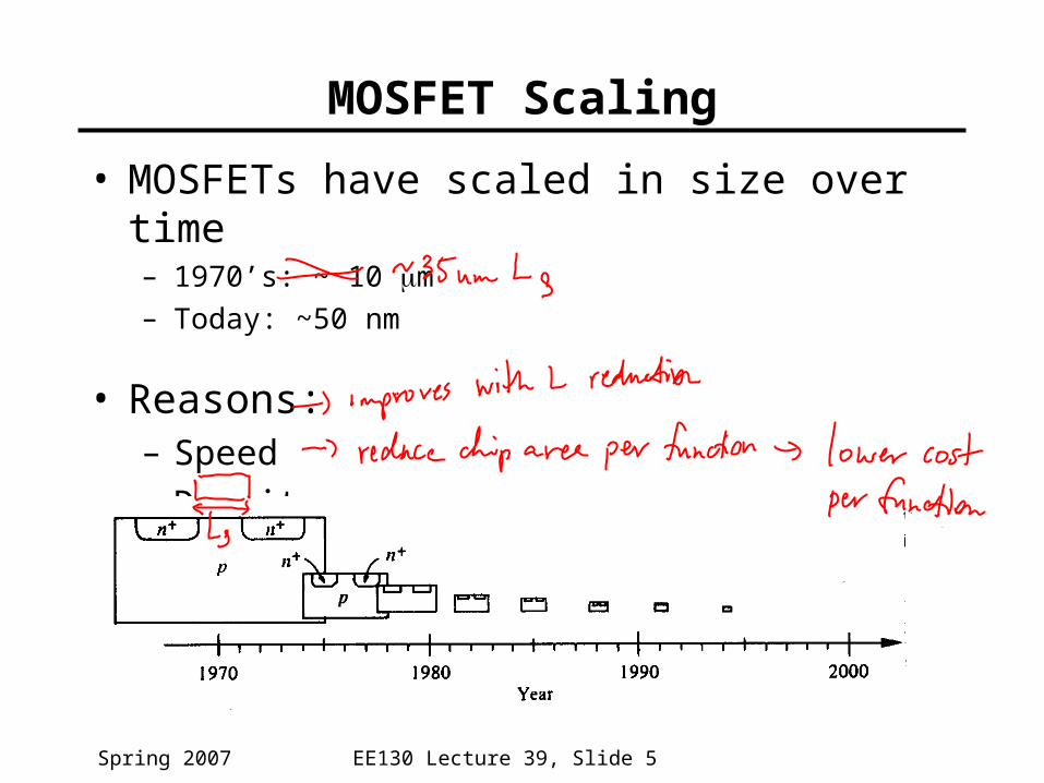
MOSFET Scaling
• MOSFETs have scaled in size over time– 1970’s: ~ 10 m– Today: ~50 nm
• Reasons:– Speed– Density
EE130 Lecture 39, Slide 6Spring 2007
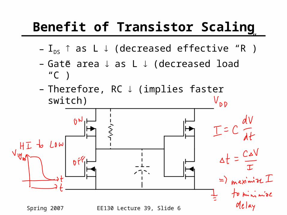
– IDS as L (decreased effective “R”)
– Gate area as L (decreased load “C”)– Therefore, RC (implies faster switch)
Benefit of Transistor Scaling
EE130 Lecture 39, Slide 7Spring 2007
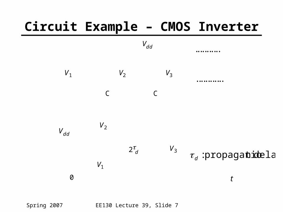
C C
V1 V2 V3
Vdd
Vdd
0
V2
V1
t
V32d
...........
............ (a)
(b) delaynpropagatio:d
Circuit Example – CMOS Inverter

EE130 Lecture 39, Slide 8Spring 2007
dsatN
dd
dsatP
dd
d
I
CVdelaydownpull
I
CVdelayuppull
delayuppulldelaydownpull
2
2
)(2
1
)11
(4 dsatPdsatN
ddd II
CV
)|(|22and
ddgdsat
dd
on
ddPN VVI
V
I
VRR
d is reduced by increasing IDsat
EE130 Lecture 39, Slide 9Spring 2007
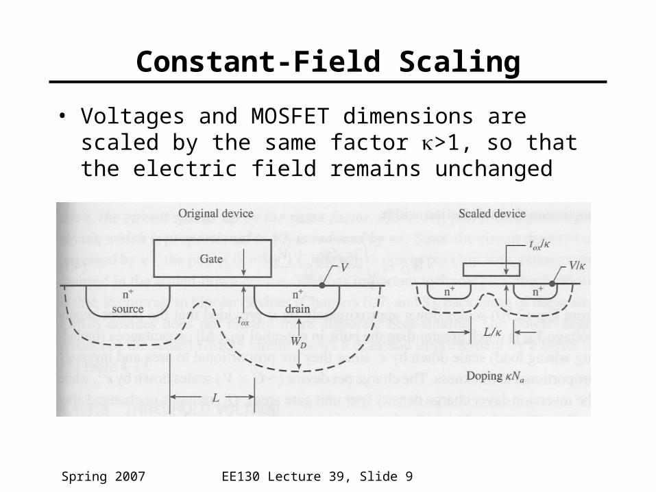
Constant-Field Scaling
• Voltages and MOSFET dimensions are scaled by the same factor >1, so that the electric field remains unchanged
EE130 Lecture 39, Slide 10Spring 2007
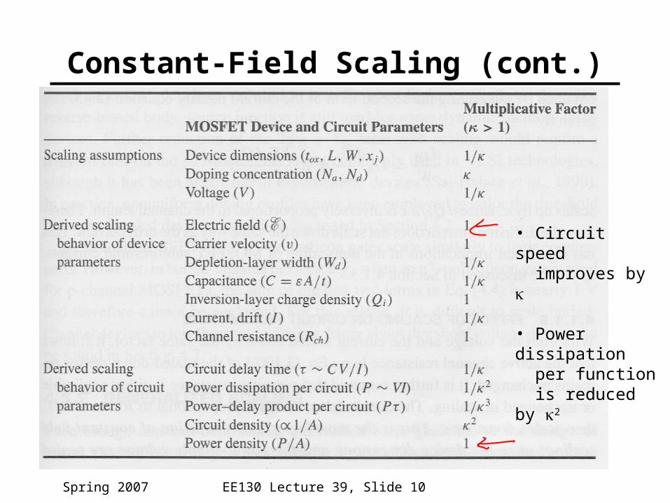
Constant-Field Scaling (cont.)
• Circuit speed improves by
• Power dissipation per function is reduced by 2
EE130 Lecture 39, Slide 11Spring 2007
VT Design Trade-Off
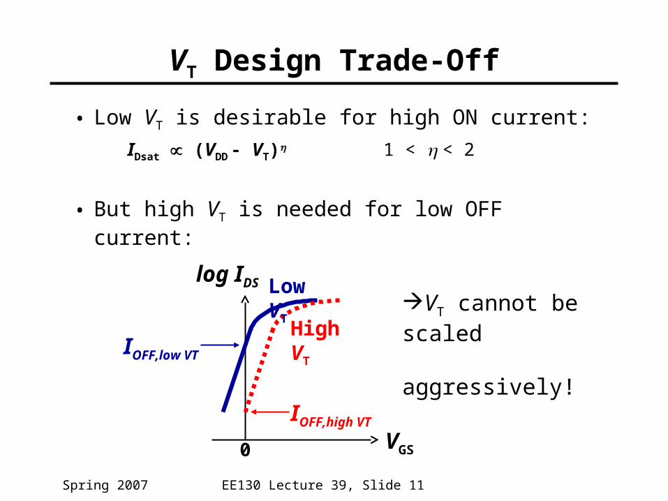
• Low VT is desirable for high ON current:
IDsat (VDD - VT) 1 < < 2
• But high VT is needed for low OFF current:
VT cannot be scaled aggressively!
Low VT
High VT
IOFF,high VT
IOFF,low VT
VGS
log IDS
0
EE130 Lecture 39, Slide 12Spring 2007
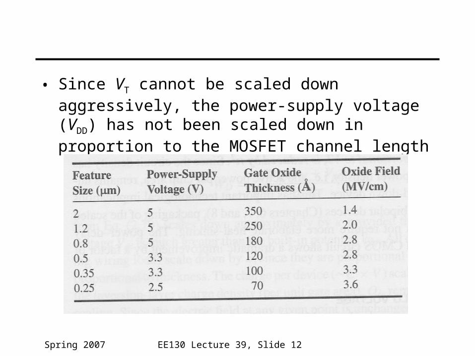
• Since VT cannot be scaled down aggressively, the power-supply voltage (VDD) has not been scaled down in proportion to the MOSFET channel length
EE130 Lecture 39, Slide 13Spring 2007
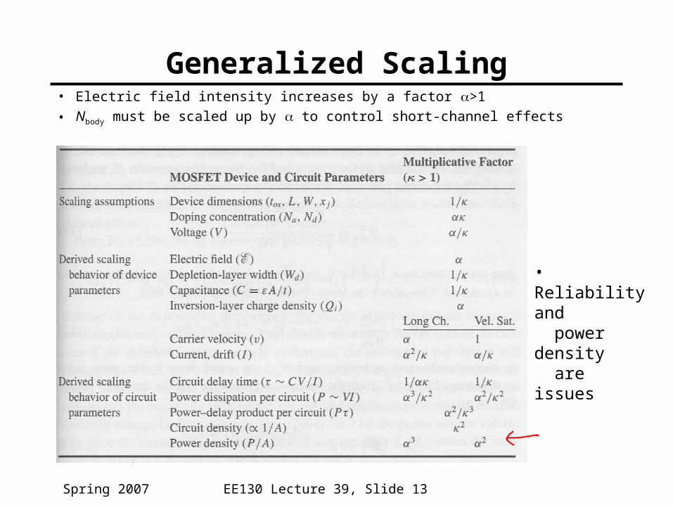
Generalized Scaling• Electric field intensity increases by a factor >1
• Nbody must be scaled up by to control short-channel effects
• Reliability and power density are issues
EE130 Lecture 39, Slide 14Spring 2007
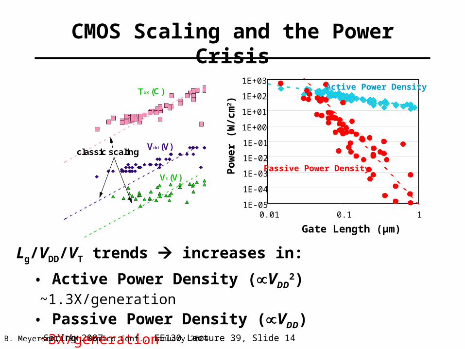
CMOS Scaling and the Power Crisis
1E-05
1E-04
1E-03
1E-02
1E-01
1E+00
1E+01
1E+02
1E+03
0.01 0.1 1
Gate Length (μm)P
ow
er (
W/c
m2 )
Passive Power Density
Active Power Density
Lg/VDD/VT trends increases in:
• Active Power Density (VDD2) ~1.3X/generation
• Passive Power Density (VDD) ~3X/generation
• Gate Leakage Power Density >4X/generationSource: B. Meyerson, IBM, Semico Conf., January 2004