Embed Size (px)
Citation preview
EE130 Lecture 25, Slide 1Spring 2007
Lecture #25
OUTLINE
• BJT: Deviations from the Ideal– Base-width modulation, Early voltage– Punch-through– Non-ideal effects at low |VEB|, high |VEB|
• Gummel plot
Reading: Chapter 11.2
Measured BJTCommon-Emitter
Output Characteristics:
EE130 Lecture 25, Slide 2Spring 2007
WNDn
LNDn
I
I
BEiE
EEBiB
LW
LW
NN
DD
n
ndcB
C
BEE
B
B
E
iB
iE
2
2
2
21
1
2
2
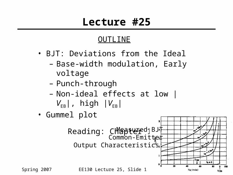
Base-Width Modulation
P+ N P
W
W(VBC)x
pB(x)
1/0 kTqV
BEBep
(VCB=0)
0
+ VEB
IE IC
Common-Emitter Configuration, Active Mode Operation
VEC
IC

EE130 Lecture 25, Slide 3Spring 2007
The base-width modulation effect is reduced if we
(a) increase the base width, W, or
(b) increase the base dopant concentration, NB, or
(c) decrease the collector dopant concentration, NC .
Which of the above is the most acceptable action?

EE130 Lecture 25, Slide 4Spring 2007
Output resistance:C
A
EC
C
I
V
V
Ir
1
0
A large VA (i.e. a large ro ) is desirable
IB3
IC
VEC0
IB2
IB1
Early Voltage, VA
VA
EE130 Lecture 25, Slide 5Spring 2007
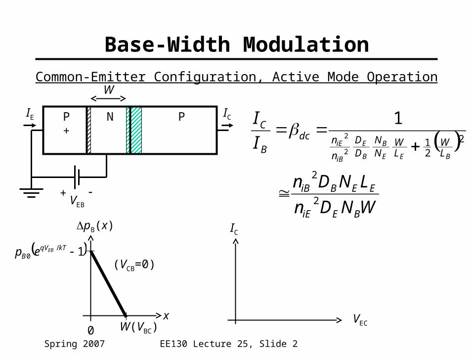
Derivation of Formula for VA
00
g
IV
V
I
dV
dIg C
AA
C
EC
C Output conductance:
for fixed VEBBC
C
EC
CoBCEBEC dV
dI
dV
dIgVVV so
BC
nCC
BC
Co dV
dx
dW
dI
dV
dW
dW
dIg
where xnC is the width of the collector-junction depletion region on the base side
P+ N P
xnC
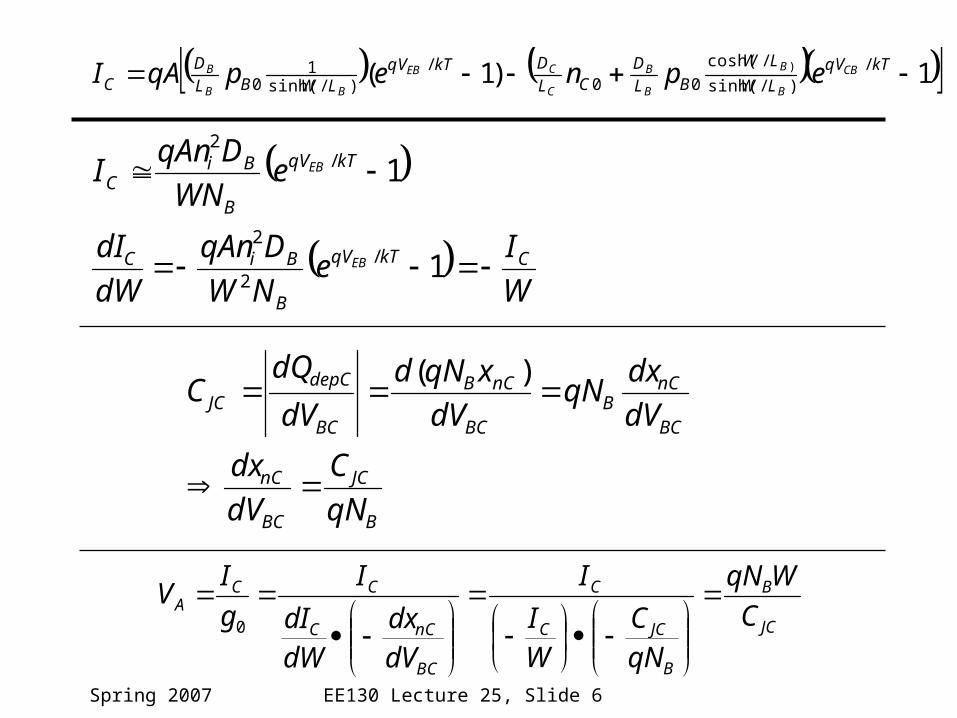
EE130 Lecture 25, Slide 6Spring 2007
W
Ie
NW
DqAn
dW
dI
eWN
DqAnI
CkTqV
B
BiC
kTqV
B
BiC
EB
EB
1
1
/2
2
/2
B
JC
BC
nC
BC
nCB
BC
nCB
BC
depCJC
qN
C
dV
dx
dV
dxqN
dV
xqNd
dV
dQC
)(
1)1( /)/sinh(
/cosh(
00/
)/sinh(1
0) kTqV
LW
LW
BLD
CLDkTqV
LWBLD
CCB
B
B
B
B
C
CEB
BB
B epnepqAI
JC
B
B
JCC
C
BC
nCC
CCA C
WqN
qNC
WI
I
dVdx
dWdI
I
g
IV
0

EE130 Lecture 25, Slide 7Spring 2007
BJT Breakdown Mechanisms• In the common-emitter configuration, for high output
voltage VCE, the output current IC will increase rapidly due to one of two mechanisms:– punch-through
– avalanche
EE130 Lecture 25, Slide 8Spring 2007
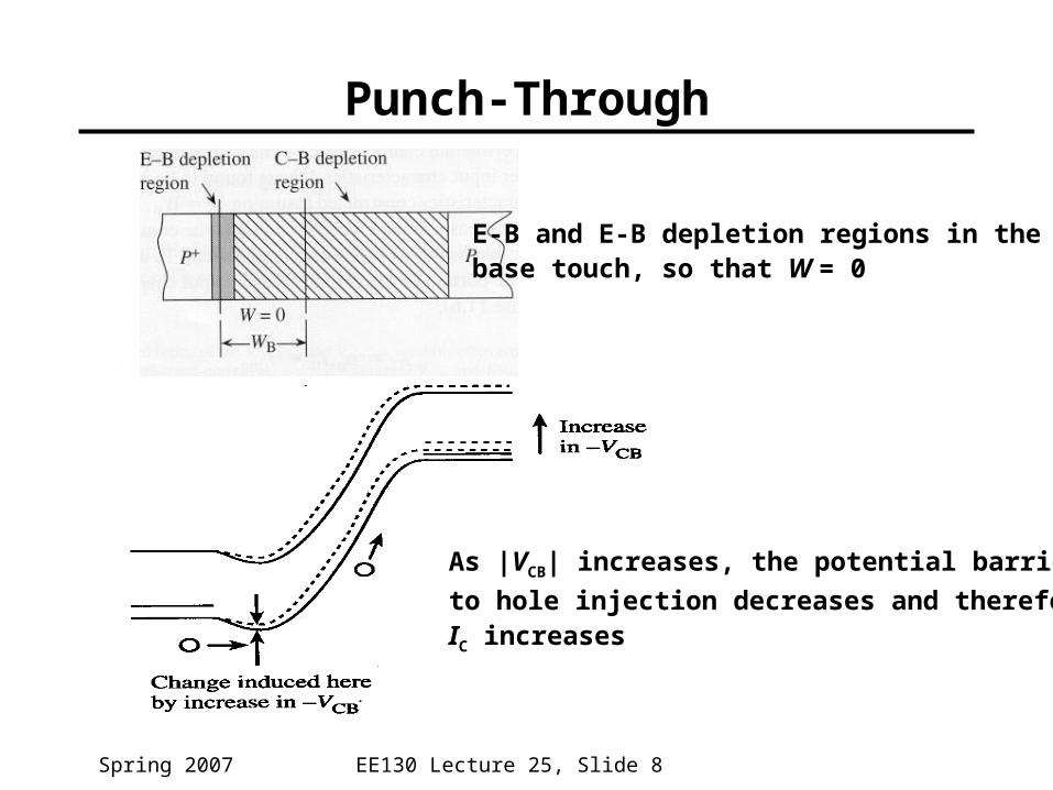
Punch-Through
E-B and E-B depletion regions in the base touch, so that W = 0
As |VCB| increases, the potential barrier
to hole injection decreases and thereforeIC increases

EE130 Lecture 25, Slide 9Spring 2007
Avalanche Multiplication• Holes are injected into the base [0], then
collected by the B-C junction– Some holes in the B-C depletion region have
enough energy to generate EHP [1]
• The generated electrons are swept into the base [3], then injected into the emitter [4]– Each injected electron results in the injection of
IEp/IEn holes from the emitter into the base [0]
PNP BJT:
For each EHP created in the C-B depletion region by impact ionization,
(IEp/IEn)+1 > dc additional holes flow into the collector
i.e. carrier multiplication in C-B depletion region is internally amplified
mdc
CBCE
VV
/10
0 )1(
where VCB0 = reverse breakdown voltage of the C-B junction
62 m
EE130 Lecture 25, Slide 10Spring 2007
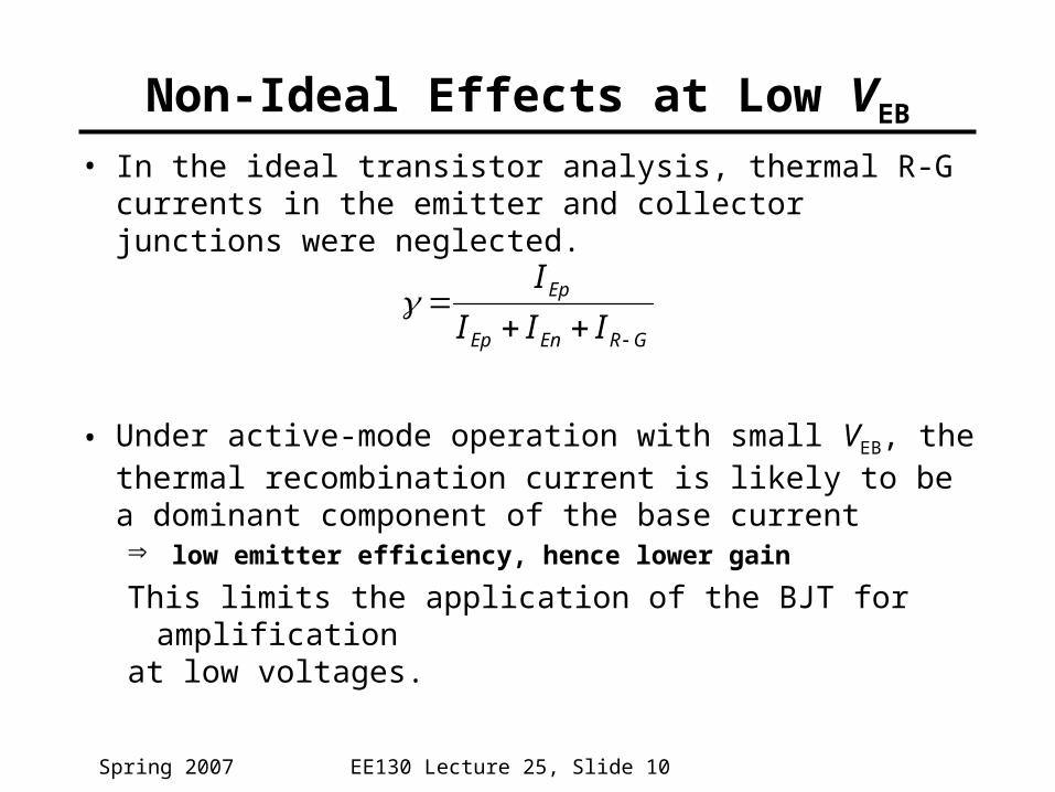
Non-Ideal Effects at Low VEB
• In the ideal transistor analysis, thermal R-G currents in the emitter and collector junctions were neglected.
• Under active-mode operation with small VEB, the thermal recombination current is likely to be a dominant component of the base current low emitter efficiency, hence lower gain
This limits the application of the BJT for amplification at low voltages.
GREnEp
Ep
III
I
EE130 Lecture 25, Slide 11Spring 2007
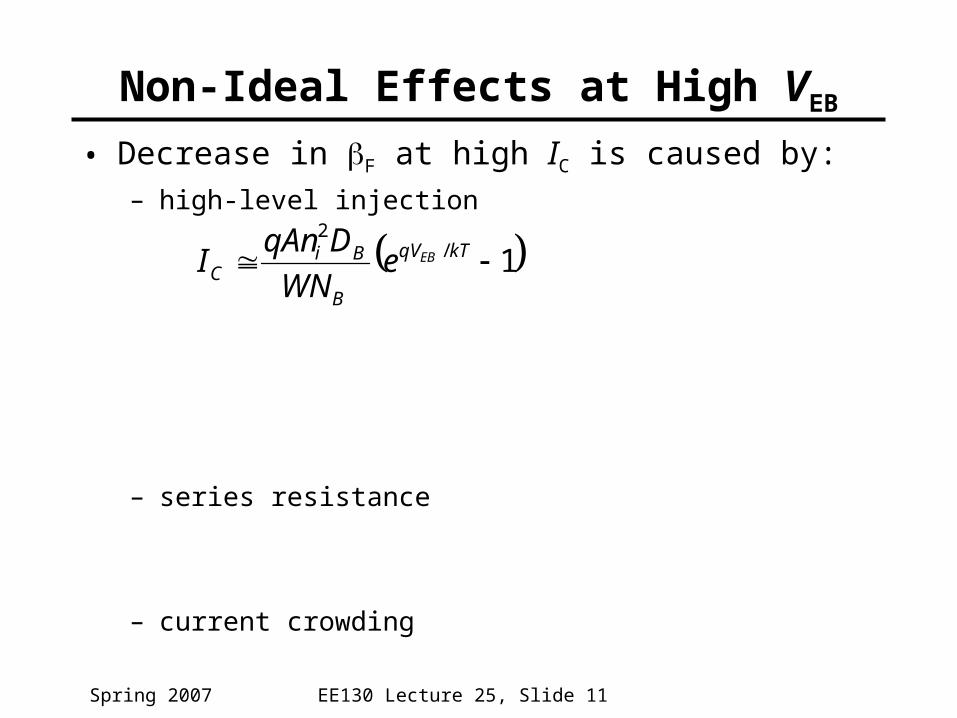
Non-Ideal Effects at High VEB
• Decrease in F at high IC is caused by:– high-level injection
– series resistance
– current crowding
1/2
kTqV
B
BiC
EBeWN
DqAnI

EE130 Lecture 25, Slide 12Spring 2007
dc
From top to bottom:VBC = 2V, 1V, 0V
0.2 0.4 0.6 0.8 1.0 1.210-12
10-10
10-8
10-6
10-4
10-2
VBE
IB
IC
excess base current due to R-G in depletion region
high level injection in base
Gummel Plot and dc vs. IC
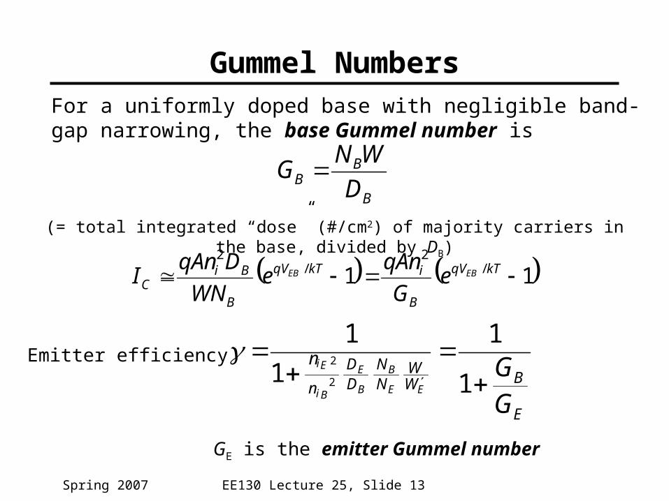
EE130 Lecture 25, Slide 13Spring 2007
Gummel NumbersFor a uniformly doped base with negligible band-gap narrowing, the base Gummel number is
B
BB D
WNG
(= total integrated “dose” (#/cm2) of majority carriers in the base, divided by DB)
E
BWW
NN
DD
nGG
EE
B
B
E
Bi
Ein
1
1
1
1
2
2Emitter efficiency
11 /2
/2
kTqV
B
ikTqV
B
BiC
EBEB eG
qAne
WN
DqAnI
GE is the emitter Gummel number

EE130 Lecture 25, Slide 14Spring 2007
dxxD
xN
n
nG
B
BW
Bi
iB )(
)(0 2
2
B
E
LW
LW
NN
DD
n
dc G
G
BEE
B
B
E
Bi
Ein
2
21
2
2
1Notice that
In real BJTs, NB and NE are not uniform, i.e. they are functions of x
The more general formulas for the Gummel numbers are
dxxD
xN
n
nG
E
EW
Ei
iE )(
)(0 2
2

EE130 Lecture 25, Slide 15Spring 2007
• High gain (dc >> 1)
One-sided emitter junction, so emitter efficiency 1• Emitter doped much more heavily than base (NE >> NB)
Narrow base, so base transport factor T 1• Quasi-neutral base width << minority-carrier diffusion length (W
<< LB)
• IC determined only by IB (IC function of VCE,VCB)
One-sided collector junction, so quasi-neutral base width W does not change drastically with changes in VCE (VCB)
• Based doped more heavily than collector (NB > NC)
(W = WB – xnEB – xnCB for PNP BJT)
Summary: BJT Performance Requirements

EE130 Lecture 25, Slide 16Spring 2007
Review: Modes of OperationCommon-emitter output characteristics
(IC vs. VCE)
Why?operation. mode active invertedfor lower is B
Cdc I
Iβ