Embed Size (px)
Citation preview

A Y1 3
Copyright © 2017, Texas Instruments Incorporated
A Y2 4
Copyright © 2017, Texas Instruments Incorporated
Product
Folder
Order
Now
Technical
Documents
Tools &
Software
Support &Community
An IMPORTANT NOTICE at the end of this data sheet addresses availability, warranty, changes, use in safety-critical applications,intellectual property matters and other important disclaimers. PRODUCTION DATA.
SN74AUP1G14SCES578J –JUNE 2003–REVISED SEPTEMBER 2017
SN74AUP1G14 Low-Power Single Schmitt-Trigger Inverter
1
1 Features1• Latch-Up Performance Exceeds 100 mA Per
JESD 78, Class II• ESD Performance Tested Per JESD 22
– 2000-V Human-Body Model(A114-B, Class II)
– 1000-V Charged-Device Model (C101)• Low Static-Power Consumption
(ICC = 0.9 µA Maximum)• Low Dynamic-Power Consumption
(Cpd = 4.4 pF Typical at 3.3 V)• Low Input Capacitance (CI = 1.5 pF Typical)• Low Noise – Overshoot and Undershoot
<10% of VCC
• Ioff Supports Partial-Power-Down Mode Operation• Includes Schmitt-Trigger Inputs• Wide Operating VCC Range of 0.8 V to 3.6 V• Optimized for 3.3-V Operation• 3.6-V I/O Tolerant to Support Mixed-Mode Signal
Operation• tpd = 4.9 ns Maximum at 3.3 V
2 Applications• AV Receivers• Smartphones• Blu-ray Players and Home Theaters• DVD Recorders and Players• Desktop or Notebook PCs• Embedded PCs• GPS: Personal Navigation Devices• Mobile Internet Devices• Portable Media Players• Smoke Detectors• Solid State Drive (SSD): Enterprise• High-Definition (HDTV)• Tablets: Enterprise• Audio Docks: Portable• DVR and DVS
3 DescriptionThe AUP family is TI's premier solution to theindustry's low power needs in battery-poweredportable applications. This family assures a very lowstatic and dynamic power consumption across theentire VCC range of 0.8 V to 3.6 V, resulting in anincreased battery life. This product also maintainsexcellent signal integrity (see AUP – The Lowest-Power Family and Excellent Signal Integrity).
This device functions as an independent gate withSchmitt-trigger inputs, which allows for slow inputtransition and better switching-noise immunity at theinput.
This device is fully specified for partial-power-downapplications using Ioff. The Ioff circuitry disables theoutputs when the device is powered down. Thisinhibits current backflow into the device whichprevents damage to the device.
Device Information(1)
PART NUMBER PACKAGE BODY SIZE (NOM)SN74AUP1G14DBV SOT-23 (5) 2.90 mm x 1.60 mmSN74AUP1G14DCK SC70 (5) 2.00 mm x 1.25 mmSN74AUP1G14DRL SOT (5) 1.60 mm x 1.20 mmSN74AUP1G14DRY SON (6) 1.45 mm x 1.00 mmSN74AUP1G14DSF SON (6) 1.00 mm x 1.00 mmSN74AUP1G14DPW X2SON (5) 0.80 mm x 0.80 mmSN74AUP1G14YFP DSBGA (4) 0.76 mm x 0.76 mm
(1) For all available packages, see the orderable addendum atthe end of the data sheet.
Logic Diagram (Positive Logic)(DBV, DCK, DRL, DRY, DSF, DPW, and YZP
Packages)
Logic Diagram (Positive Logic)(YFP Package)

2
SN74AUP1G14SCES578J –JUNE 2003–REVISED SEPTEMBER 2017 www.ti.com
Product Folder Links: SN74AUP1G14
Submit Documentation Feedback Copyright © 2003–2017, Texas Instruments Incorporated
Table of Contents1 Features .................................................................. 12 Applications ........................................................... 13 Description ............................................................. 14 Revision History..................................................... 25 Pin Configuration and Functions ......................... 36 Specifications......................................................... 4
6.1 Absolute Maximum Ratings ...................................... 46.2 ESD Ratings.............................................................. 46.3 Recommended Operating Conditions....................... 46.4 Thermal Information .................................................. 56.5 Electrical Characteristics........................................... 56.6 Switching Characteristics: CL = 5 pF ........................ 76.7 Switching Characteristics: CL = 10 pF ...................... 76.8 Switching Characteristics: CL = 15 pF ...................... 86.9 Switching Characteristics: CL = 30 pF ...................... 86.10 Operating Characteristics........................................ 86.11 Typical Characteristics ............................................ 9
7 Parameter Measurement Information ................ 107.1 (Propagation Delays, Setup and Hold Times, and
Pulse Width)............................................................. 107.2 (Enable and Disable Times).................................... 11
8 Detailed Description ............................................ 128.1 Overview ................................................................. 128.2 Functional Block Diagrams ..................................... 128.3 Feature Description................................................. 128.4 Device Functional Modes........................................ 13
9 Application and Implementation ........................ 149.1 Application Information............................................ 149.2 Typical Application .................................................. 14
10 Power Supply Recommendations ..................... 1611 Layout................................................................... 16
11.1 Layout Guidelines ................................................. 1611.2 Layout Example .................................................... 16
12 Device and Documentation Support ................. 1712.1 Documentation Support ........................................ 1712.2 Receiving Notification of Documentation Updates 1712.3 Community Resources.......................................... 1712.4 Trademarks ........................................................... 1712.5 Electrostatic Discharge Caution............................ 1712.6 Glossary ................................................................ 17
13 Mechanical, Packaging, and OrderableInformation ........................................................... 17
4 Revision HistoryNOTE: Page numbers for previous revisions may differ from page numbers in the current version.
Changes from Revision I (May 2010) to Revision J Page
• Added DPW (X2SON) package.............................................................................................................................................. 1• Added Device Information table, Pin Configuration and Functions section, ESD Ratings table, Thermal Information
table, Feature Description section, Device Functional Modes, Application and Implementation section, Power SupplyRecommendations section, Layout section, Device and Documentation Support section, and Mechanical,Packaging, and Orderable Information section. ..................................................................................................................... 1
• Deleted Ordering Information table, see Mechanical, Packaging, and Orderable Information section at the end of thedata sheet .............................................................................................................................................................................. 1
• Changed formatting of YFP package pinout drawing ............................................................................................................ 3• Deleted YZP package from data sheet ................................................................................................................................. 3• Added Junction temperature, TJ in Absolute Maximum Ratings ............................................................................................ 4

Y
VCC
A
NCGND
GND Y3 4
A 2 5
NC 61
NC
VCC
GND
A NC
NC 6
5
4
2
3 Y
VCC
1
1 2
B
A
Not to scale
GND Y
A VCC
3
2
4
51NC VCC
Y
A
GND
3
2
4
51NC VCC
Y
A
GND
3
2
4
51NC VCC
Y
A
GND
3
SN74AUP1G14www.ti.com SCES578J –JUNE 2003–REVISED SEPTEMBER 2017
Product Folder Links: SN74AUP1G14
Submit Documentation FeedbackCopyright © 2003–2017, Texas Instruments Incorporated
5 Pin Configuration and Functions
DBV Package5-Pin SOT-23
Top ViewDCK Package
5-Pin SC70Top View
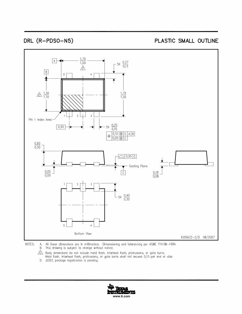
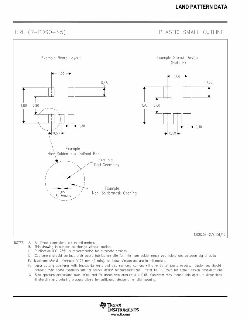
DRL Package5-Pin SOTTop View
YFP Package4-Pin DSBGABottom View
N.C. – No internal connection.See mechancial drawings for dimensions.
DRY Package6-Pin SONTop View
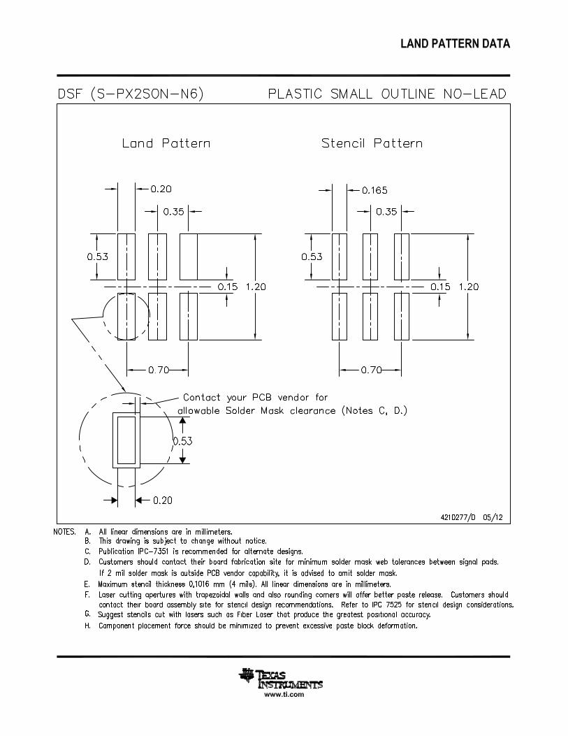
DSF Package6-Pin SONTop View
DPW Package5-Pin X2SON
Top View
Pin FunctionsPIN
I/O DESCRIPTIONNAME DBV, DCK,
DRL, DPW DRY, DSF YFP
A 2 2 A1 I Logic InputGND 3 3 B1 — GroundN.C. 1 1, 5 — — No internal connectionVCC 5 6 A2 — Positive SupplyY 4 4 B2 O Output

4
SN74AUP1G14SCES578J –JUNE 2003–REVISED SEPTEMBER 2017 www.ti.com
Product Folder Links: SN74AUP1G14
Submit Documentation Feedback Copyright © 2003–2017, Texas Instruments Incorporated
(1) Stresses beyond those listed under "absolute maximum ratings" may cause permanent damage to the device. These are stress ratingsonly, and functional operation of the device at these or any other conditions beyond those indicated under "recommended operatingconditions" is not implied. Exposure to absolute-maximum-rated conditions for extended periods may affect device reliability.
(2) The input and output negative-voltage ratings may be exceeded if the input and output current ratings are observed.
6 Specifications
6.1 Absolute Maximum Ratingsover operating free-air temperature range (unless otherwise noted) (1)
MIN MAX UNITVCC Supply voltage –0.5 4.6 VVI Input voltage (2) –0.5 4.6 VVO Voltage range applied to any output in the high-impedance or power-off state (2) –0.5 4.6 VVO Voltage range applied to any output in the high or low state (2) –0.5 VCC + 0.5 VIIK Input clamp current VI < 0 –50 mAIOK Output clamp current VO < 0 –50 mAIO Continuous output current ±20 mA
Continuous current through VCC or GND ±50 mATJ Junction temperature 150 °CTstg Storage temperature –65 150 °C
(1) JEDEC document JEP155 states that 500-V HBM allows safe manufacturing with a standard ESD control process.(2) JEDEC document JEP157 states that 250-V CDM allows safe manufacturing with a standard ESD control process.
6.2 ESD RatingsVALUE UNIT
V(ESD) Electrostatic dischargeHuman-body model (HBM), per ANSI/ESDA/JEDEC JS-001 (1) 2000
VCharged-device model (CDM), per JEDEC specification JESD22-C101 (2) 1000
(1) All unused inputs of the device must be held at VCC or GND to assure proper device operation. See Implications of Slow or FloatingCMOS Inputs.
6.3 Recommended Operating ConditionsSee (1)
MIN MAX UNITVCC Supply voltage 0.8 3.6 VVI Input voltage 0 3.6 VVO Output voltage 0 VCC V
IOH High-level output current
VCC = 0.8 V –20 µAVCC = 1.1 V –1.1
mAVCC = 1.4 V –1.7VCC = 1.65 V –1.9VCC = 2.3 V –3.1VCC = 3 V –4
IOL Low-level output current
VCC = 0.8 V 20 µAVCC = 1.1 V 1.1
mAVCC = 1.4 V 1.7VCC = 1.65 V 1.9VCC = 2.3 V 3.1VCC = 3 V 4
TA Operating free-air temperature –40 85 °C

5
SN74AUP1G14www.ti.com SCES578J –JUNE 2003–REVISED SEPTEMBER 2017
Product Folder Links: SN74AUP1G14
Submit Documentation FeedbackCopyright © 2003–2017, Texas Instruments Incorporated
(1) For more information about traditional and new thermal metrics, see the Semiconductor and IC Package Thermal Metrics applicationreport.
6.4 Thermal Information
THERMAL METRIC (1)
SN74AUP1G14
UNITDRY(SON)
DSF(SON)
YFP(DSBGA)
DPW(X2SON)
DBV(SOT-23)
DCK(SC70)
DRL(SOT)
6 PINS 6 PINS 4 PINS 5 PINS 5 PINS 5 PINS 5 PINS
RθJA Junction-to-ambient thermal resistance 347.8 386.2 179.3 489.2 289.1 325.1 324.4 °C/W
RθJC(top) Junction-to-case (top) thermal resistance 237.7 192.9 2.8 226.3 213.7 229.1 156.7 °C/W
RθJB Junction-to-board thermal resistance 210.6 242.2 58.3 352.9 123.0 123.2 172.9 °C/W
ψJTJunction-to-top characterizationparameter 64.4 28.9 1.1 38.2 104.5 96.3 21.6 °C/W
ψJBJunction-to-board characterizationparameter 210.6 241.9 58.6 352.1 122.3 122.4 173.6 °C/W
RθJC(bot)Junction-to-case (bottom) thermalresistance N/A N/A N/A 150.8 N/A N/A N/A °C/W
6.5 Electrical Characteristicsover operating free-air temperature range (unless otherwise noted)
PARAMETER TEST CONDITIONS VCC MIN TYP MAX UNIT
VT+Positive-going inputthreshold voltage
TA = 25°C0.8 V 0.3 0.6
V
TA = –40°C to +85°C
TA = 25°C1.1 V 0.53 0.9
TA = –40°C to +85°C
TA = 25°C1.4 V 0.74 1.11
TA = –40°C to +85°C
TA = 25°C1.65 V 0.91 1.29
TA = –40°C to +85°C
TA = 25°C2.3 V 1.37 1.77
TA = –40°C to +85°C
TA = 25°C3 V 1.88 2.29
TA = –40°C to +85°C
VT–Negative-going inputthreshold voltage
TA = 25°C0.8 V 0.1 0.6
V
TA = –40°C to +85°C
TA = 25°C1.1 V 0.26 0.65
TA = –40°C to +85°C
TA = 25°C1.4 V 0.39 0.75
TA = –40°C to +85°C
TA = 25°C1.65 V 0.47 0.84
TA = –40°C to +85°C
TA = 25°C2.3 V 0.69 1.04
TA = –40°C to +85°C
TA = 25°C3 V 0.88 1.24
TA = –40°C to +85°C

6
SN74AUP1G14SCES578J –JUNE 2003–REVISED SEPTEMBER 2017 www.ti.com
Product Folder Links: SN74AUP1G14
Submit Documentation Feedback Copyright © 2003–2017, Texas Instruments Incorporated
Electrical Characteristics (continued)over operating free-air temperature range (unless otherwise noted)
PARAMETER TEST CONDITIONS VCC MIN TYP MAX UNIT
ΔVTHysteresis(VT+ – VT– )
TA = 25°C0.8 V 0.07 0.5
V
TA = –40°C to +85°C
TA = 25°C1.1 V 0.08 0.46
TA = –40°C to +85°C
TA = 25°C1.4 V 0.18 0.56
TA = –40°C to +85°C
TA = 25°C1.65 V 0.27 0.66
TA = –40°C to +85°C
TA = 25°C2.3 V 0.53 0.92
TA = –40°C to +85°C
TA = 25°C3 V 0.79 1.31
TA = –40°C to +85°C
VOH
IOH = –20 µATA = 25°C
0.8 V to 3.6 V VCC – 0.1
V
TA = –40°C to +85°C
IOH = –1.1 mATA = 25°C
1.1 V0.75 × VCC
TA = –40°C to +85°C 0.7 × VCC
IOH = –1.7 mATA = 25°C
1.4 V1.11
TA = –40°C to +85°C 1.03
IOH = –1.9 mATA = 25°C
1.65 V1.32
TA = –40°C to +85°C 1.3
IOH = –2.3 mATA = 25°C
2.3 V
2.05
TA = –40°C to +85°C 1.97
IOH = –3.1 mATA = 25°C 1.9
TA = –40°C to +85°C 1.85
IOH = –2.7 mATA = 25°C
3 V
2.72
TA = –40°C to +85°C 2.67
IOH = –4 mATA = 25°C 2.6
TA = –40°C to +85°C 2.55
VOL
IOL = 20 μATA = 25°C
0.8 V to 3.6 V 0.1
V
TA = –40°C to +85°C
IOL = 1.1 mATA = 25°C
1.1 V 0.3 ×VCCTA = –40°C to +85°C
IOL = 1.7 mATA = 25°C
1.4 V0.31
TA = –40°C to +85°C 0.37
IOL = 1.9 mATA = 25°C
1.65 V0.31
TA = –40°C to +85°C 0.35
IOL = 2.3 mATA = 25°C
2.3 V
0.31
TA = –40°C to +85°C 0.33
IOL = 3.1 mATA = 25°C 0.44
TA = –40°C to +85°C 0.45
IOL = 2.7 mATA = 25°C
3 V
0.31
TA = –40°C to +85°C 0.33
IOL = 4 mATA = 25°C 0.44
TA = –40°C to +85°C 0.45
II A input VI = GND to 3.6 VTA = 25°C
0 V to 3.6 V0.1
µATA = –40°C to +85°C 0.5
IOFFVI orVO = 0 V to 3.6 V
TA = 25°C0 V
0.2µA
TA = –40°C to +85°C 0.6
ΔI OFFVI orVO = 0 V to 3.6 V
TA = 25°C0 V to 0.2 V
0.2
TA = –40°C to +85°C 0.6

7
SN74AUP1G14www.ti.com SCES578J –JUNE 2003–REVISED SEPTEMBER 2017
Product Folder Links: SN74AUP1G14
Submit Documentation FeedbackCopyright © 2003–2017, Texas Instruments Incorporated
Electrical Characteristics (continued)over operating free-air temperature range (unless otherwise noted)
PARAMETER TEST CONDITIONS VCC MIN TYP MAX UNIT
ICCVI = GND or (VCC to 3.6 V)IO = 0
TA = 25°C0.8 V to 3.6 V
0.5µA
TA = –40°C to +85°C 0.9
ΔICCVI = VCC – 0.6 VIO = 0
TA = 25°C3.3 V
40µA
TA = –40°C to +85°C 50
CI VI = VCC or GNDTA = –40°C to +85°C 0 V
1.5 pFTA = –40°C to +85°C 3.6 V
CO VO = GND TA = –40°C to +85°C 0 V 2.5 pF
6.6 Switching Characteristics: CL = 5 pFover recommended operating free-air temperature range, CL = 5 pF (unless otherwise noted) (see Figure 2 and Figure 3)
PARAMETER FROM(INPUT)
TO(OUTPUT) TEST CONDITIONS MIN TYP MAX UNIT
tpd A Y
VCC = 0.8 V TA = 25°C 16.3
ns
VCC = 1.2 V ± 0.1 VTA = 25°C 4.2 6.9 11.7TA = –40°C to +85°C 0.9 15
VCC = 1.5 V ± 0.1 VTA = 25°C 3.7 5.2 8.4TA = –40°C to +85°C 1.7 10.7
VCC = 1.8 V ± 0.15 VTA = 25°C 3.3 4.4 6.9TA = –40°C to +85°C 1.9 8.5
VCC = 2.5 V ± 0.2 VTA = 25°C 2.8 3.5 4.8TA = –40°C to +85°C 1.8 6.1
VCC = 3.3 V ± 0.3 VTA = 25°C 2.5 3 4TA = –40°C to +85°C 1.7 4.9
6.7 Switching Characteristics: CL = 10 pFover recommended operating free-air temperature range, CL = 10 pF (unless otherwise noted) (see Figure 2 and Figure 3)
PARAMETER FROM(INPUT)
TO(OUTPUT) TEST CONDITIONS MIN TYP MAX UNIT
tpd A Y
VCC = 0.8 V TA = 25°C 18.4
ns
VCC = 1.2 V ± 0.1 VTA = 25°C 4.6 7.9 13.4TA = –40°C to +85°C 1.3 16.7
VCC = 1.5 V ± 0.1 VTA = 25°C 4 6 9.6TA = –40°C to +85°C 2.2 11.8
VCC = 1.8 V ± 0.15 VTA = 25°C 3.6 5 7.9TA = –40°C to +85°C 2.4 9.5
VCC = 2.5 V ± 0.2 VTA = 25°C 3.2 4 5.5TA = –40°C to +85°C 2.3 6.8
VCC = 3.3 V ± 0.3 VTA = 25°C 2.9 3.5 4.6TA = –40°C to +85°C 2.1 5.6

8
SN74AUP1G14SCES578J –JUNE 2003–REVISED SEPTEMBER 2017 www.ti.com
Product Folder Links: SN74AUP1G14
Submit Documentation Feedback Copyright © 2003–2017, Texas Instruments Incorporated
6.8 Switching Characteristics: CL = 15 pFover recommended operating free-air temperature range, CL = 15 pF (unless otherwise noted) (see Figure 2 and Figure 3)
PARAMETER FROM(INPUT)
TO(OUTPUT) TEST CONDITIONS MIN TYP MAX UNIT
tpd A Y
VCC = 0.8 V TA = 25°C 20.1
ns
VCC = 1.2 V ± 0.1 VTA = 25°C 5.5 8.7 14TA = –40°C to +85°C 2.5 17.3
VCC = 1.5 V ± 0.1 VTA = 25°C 4.7 6.7 10TA = –40°C to +85°C 3 12.5
VCC = 1.8 V ± 0.15 VTA = 25°C 4.2 5.6 8.3TA = –40°C to +85°C 3 10.1
VCC = 2.5 V ± 0.2 VTA = 25°C 3.6 4.5 5.9TA = –40°C to +85°C 2.7 7.4
VCC = 3.3 V ± 0.3 VTA = 25°C 3.3 3.9 5TA = –40°C to +85°C 2.5 6.1
6.9 Switching Characteristics: CL = 30 pFover recommended operating free-air temperature range, CL = 30 pF (unless otherwise noted) (see Figure 2 and Figure 3)
PARAMETER FROM(INPUT)
TO(OUTPUT) TEST CONDITIONS MIN TYP MAX UNIT
tpd A Y
VCC = 0.8 V TA = 25°C 25.7
ns
VCC = 1.2 V ± 0.1 VTA = 25°C 7.4 11.2 17.1TA = –40°C to +85°C 4.5 20.5
VCC = 1.5 V ± 0.1 VTA = 25°C 6.1 8.5 12.3TA = –40°C to +85°C 4.6 14.7
VCC = 1.8 V ± 0.15 VTA = 25°C 5.4 7.2 10.3TA = –40°C to +85°C 4.1 12
VCC = 2.5 V ± 0.2 VTA = 25°C 4.7 5.7 7.4TA = –40°C to +85°C 3.7 8.8
VCC = 3.3 V ± 0.3 VTA = 25°C 4.2 5 6.2TA = –40°C to +85°C 3.5 7.3
6.10 Operating CharacteristicsTA = 25°C
PARAMETER TEST CONDITIONS VCC TYP UNIT
Cpd Power dissipation capacitance f = 10 MHz
0.8 V 4
pF
1.2 V ± 0.1 V 41.5 V ± 0.1 V 4.11.8 V ± 0.15 V 4.12.5 V ± 0.2 V 4.33.3 V ± 0.3 V 4.4

VCC
t pd
(TY
P)
[ns]
0.75 1 1.25 1.5 1.75 2 2.25 2.5 2.75 3 3.25 3.52
4
6
8
10
12
14
16
18
20
22
tpd_tpd_
TA = 25qC
9
SN74AUP1G14www.ti.com SCES578J –JUNE 2003–REVISED SEPTEMBER 2017
Product Folder Links: SN74AUP1G14
Submit Documentation FeedbackCopyright © 2003–2017, Texas Instruments Incorporated
6.11 Typical Characteristics
Figure 1. Typical Propagation Delay vs. Supply Voltage (CL = 15 pF

VM
From OutputUnder Test
CL(see Note A)
LOAD CIRCUIT
1 MΩ
VOLTAGE WAVEFORMSPROPAGATION DELAY TIMES
INVERTING AND NONINVERTING OUTPUTS
tPLH
tPHL
tPHL
tPLH
VOH
VOH
VOL
VOL
VI
0 VInput
Output
Output
NOTES: A. CL includes probe and jig capacitance.B. All input pulses are supplied by generators having the following characteristics: PRR ≤ 10 MHz, ZO = 50 Ω, tr/tf = 3 ns.C. The outputs are measured one at a time, with one transition per measurement.D. tPLH and tPHL are the same as tpd.E. All parameters and waveforms are not applicable to all devices.
VM VM
VM VM
VM
5, 10, 15, 30 pFVCC/2VCC
VCC = 1.2 V± 0.1 V
VCC = 0.8 VVCC = 1.5 V
± 0.1 VVCC = 1.8 V
± 0.15 VVCC = 2.5 V
± 0.2 VVCC = 3.3 V
± 0.3 V
5, 10, 15, 30 pFVCC/2VCC
5, 10, 15, 30 pFVCC/2VCC
5, 10, 15, 30 pFVCC/2VCC
CLVMVI
5, 10, 15, 30 pFVCC/2VCC
5, 10, 15, 30 pFVCC/2VCC
thtsu
Data Input
Timing InputVCC
0 V
VCC
0 V
0 V
tw
Input
VOLTAGE WAVEFORMSSETUP AND HOLD TIMES
VOLTAGE WAVEFORMSPULSE DURATION
VCC/2 VCC/2
VCC/2
VCC/2
VCC
VCC/2
10
SN74AUP1G14SCES578J –JUNE 2003–REVISED SEPTEMBER 2017 www.ti.com
Product Folder Links: SN74AUP1G14
Submit Documentation Feedback Copyright © 2003–2017, Texas Instruments Incorporated
7 Parameter Measurement Information
7.1 (Propagation Delays, Setup and Hold Times, and Pulse Width)
Figure 2. Load Circuit And Voltage Waveforms

NOTES: A. CL includes probe and jig capacitance.B. Waveform 1 is for an output with internal conditions such that the output is low, except when disabled by the output control.
Waveform 2 is for an output with internal conditions such that the output is high, except when disabled by the output control.C. All input pulses are supplied by generators having the following characteristics: PRR ≤ 10 MHz, ZO = 50 Ω, tr/tf = 3 ns.D. The outputs are measured one at a time, with one transition per measurement.E. tPLZ and tPHZ are the same as tdis.F. tPZL and tPZH are the same as ten.G. All parameters and waveforms are not applicable to all devices.
5, 10, 15, 30 pFVCC/2VCC
0.15 V
VCC = 1.2 V± 0.1 V
VCC = 0.8 VVCC = 1.5 V
± 0.1 VVCC = 1.8 V
± 0.15 VVCC = 2.5 V
± 0.2 VVCC = 3.3 V
± 0.3 V
5, 10, 15, 30 pFVCC/2VCC0.1 V
5, 10, 15, 30 pFVCC/2VCC0.1 V
5, 10, 15, 30 pFVCC/2VCC0.1 V
CLVMVIV∆
5, 10, 15, 30 pFVCC/2VCC
0.15 V
5, 10, 15, 30 pFVCC/2VCC0.3 V
OutputWaveform 1
S1 at 2 × VCC(see Note B)
OutputWaveform 2
S1 at GND(see Note B)
VOL
VOH
tPZL
tPZH
tPLZ
tPHZ
VCC
0 V
VOL + V∆
VOH - V∆
≈0 V
VCC
VOLTAGE WAVEFORMSENABLE AND DISABLE TIMES
LOW- AND HIGH-LEVEL ENABLING
OutputControl
VCC/2 VCC/2
VCC/2
VCC/2
tPLZ/tPZLtPHZ/tPZH
2 × VCCGND
TEST S1From Output
Under Test
CL(see Note A)
LOAD CIRCUIT
S1
GND
5 kΩ
5 kΩ
2 × VCC
11
SN74AUP1G14www.ti.com SCES578J –JUNE 2003–REVISED SEPTEMBER 2017
Product Folder Links: SN74AUP1G14
Submit Documentation FeedbackCopyright © 2003–2017, Texas Instruments Incorporated
7.2 (Enable and Disable Times)
Figure 3. Load Circuit And Voltage Waveforms

A Y1 3
Copyright © 2017, Texas Instruments Incorporated
A Y2 4
Copyright © 2017, Texas Instruments Incorporated
12
SN74AUP1G14SCES578J –JUNE 2003–REVISED SEPTEMBER 2017 www.ti.com
Product Folder Links: SN74AUP1G14
Submit Documentation Feedback Copyright © 2003–2017, Texas Instruments Incorporated
8 Detailed Description
8.1 OverviewThis device functions as an independent gate with Schmitt-trigger inputs, which allows for slow input transitionand better switching-noise immunity at the input.
This device is fully specified for partial-power-down applications using Ioff. The Ioff circuitry disables the outputswhen the device is powered down. This inhibits current backflow into the device which prevents damage to thedevice.
8.2 Functional Block Diagrams
Figure 4. Logic Diagram (Positive Logic)(DBV, DCK, DRL, DRY, DSF, DPW, and YZP Packages)
Figure 5. Logic Diagram (Positive Logic)(YFP Package)
8.3 Feature Description
8.3.1 Balanced CMOS Push-Pull OutputsA balanced output allows the device to sink and source similar currents. The drive capability of this devicecreates fast edges into light loads so routing and load conditions should be considered to prevent ringing.Additionally, the outputs of this device are capable of driving larger currents than the device can sustain withoutbeing damaged. It is important for the power output of the device to be limited to avoid thermal runaway anddamage due to over-current. The electrical and thermal limits defined the in the Absolute Maximum Ratings tablemust be followed at all times.
8.3.2 Schmitt-Trigger InputsStandard CMOS inputs are high impedance and are typically modeled as a resistor in parallel with the inputcapacitance given in the Electrical Characteristics table. The worst case resistance is calculated with themaximum input voltage, given in the Absolute Maximum Ratings table, and the maximum input leakage current,given in the Electrical Characteristics table, using ohm's law (R = V ÷ I).
The Schmitt-trigger input architecture provides hysteresis as defined by ΔVT in the Electrical Characteristicstable, which makes this device extremely tolerant to slow or noisy inputs. While the inputs can be driven muchslower than standard CMOS inputs, it is still recommended to properly terminate unused inputs. Driving theinputs slowly will also increase dynamic current consumption of the device. For additional information regardingSchmitt-trigger inputs, see Understanding Schmitt Triggers.

GND
LogicInput Output
VCCDevice
-IIK -IOK
13
SN74AUP1G14www.ti.com SCES578J –JUNE 2003–REVISED SEPTEMBER 2017
Product Folder Links: SN74AUP1G14
Submit Documentation FeedbackCopyright © 2003–2017, Texas Instruments Incorporated
Feature Description (continued)8.3.3 Clamp DiodesThe inputs and outputs to this device have negative clamping diodes.
CAUTIONVoltages beyond the values specified in the Absolute Maximum Ratings table cancause damage to the device. The input negative-voltage and output voltage ratingsmay be exceeded if the input and output clamp-current ratings are observed.
Figure 6. Electrical Placement of Clamping Diodes for Each Input and Output
8.3.4 Partial Power Down (Ioff)The inputs and outputs for this device enter a high impedance state when the supply voltage is 0 V. Themaximum leakage into or out of any input or output pin on the device is specified by Ioff in the ElectricalCharacteristics table.
8.3.5 Over-Voltage Tolerant InputsInput signals to this device can be driven above the supply voltage so long as they remain below the maximuminput voltage value specified in the Absolute Maximum Ratings table.
8.4 Device Functional ModesTable 1 lists the functional modes of the SN74AUP1G14.
Table 1. Function TableINPUT
AOUTPUT
YH LL H

C1
R1
A Y OUTPUT
VCC
R2
14
SN74AUP1G14SCES578J –JUNE 2003–REVISED SEPTEMBER 2017 www.ti.com
Product Folder Links: SN74AUP1G14
Submit Documentation Feedback Copyright © 2003–2017, Texas Instruments Incorporated
9 Application and Implementation
NOTEInformation in the following applications sections is not part of the TI componentspecification, and TI does not warrant its accuracy or completeness. TI’s customers areresponsible for determining suitability of components for their purposes. Customers shouldvalidate and test their design implementation to confirm system functionality.
9.1 Application InformationMechanical input elements, such as push buttons or rotary knobs, offer simple ways to interact with electronicsystems. Typically, these elements have recoil or bouncing, where the mechanical element makes and breakscontact multiple times during human interaction. This bouncing can cause one or more repeated signals to bepassed, triggering multiple actions when only a single input was intended. One potential solution to mitigatingthese multiple inputs is by utilizing a Schmitt-trigger to create a debounce circuit. Figure 7 shows an example ofthis solution.
9.2 Typical ApplicationThe input due to the push button switches multiple times, causing the output of a non Schmitt-trigger device totrigger multiple times, while the Schmitt-trigger input device with RC delay limits the output pulse to a singlepulse desired by the user. The separated positive and negative input voltage threshold values prevent multipletriggers from occurring, see the Electrical Characteristics table for VT+, VT-, and Vhys values.
Figure 7. Push Button Debounce Circuit Schematic
9.2.1 Design RequirementsThis device uses CMOS technology and has balanced output drive. Take care to avoid bus contention because itcan drive currents that would exceed maximum limits. The drive strength also creates fast edges into light loadsso routing and load conditions should be considered to prevent ringing.
9.2.2 Detailed Design Procedure1. Recommended Input Conditions:
– For specified high and low levels, see (VT+ and VT-) in the Electrical Characteristics table.– Inputs are overvoltage tolerant allowing them to go as high as (VI max) in the Recommended Operating
Conditions table at any valid VCC.2. Recommended Output Conditions:
– Load currents should not exceed (IO max) per output and should not exceed (Continuous current throughVCC or GND) total current for the part. These limits are located in the Absolute Maximum Ratings table.

−0.5
0
0.5
1
1.5
2
2.5
3
3.5
0 5 10 15 20 25 30 35 40 45
Time − ns
Voltage
−V
† AUP1G08 data at CL = 15 pF
OutputInput
Switching Characteristics
at 25 MHz†
AUP
LVC
AUPAUP
LVC
Static-Power Consumption
( A)m
Dynamic-Power Consumption
(pF)
† Single, dual, and triple gates
3.3-V
Logic †
3.3-V
Logic †
0%
20%
40%
60%
80%
100%
0%
20%
40%
60%
80%
100%
15
SN74AUP1G14www.ti.com SCES578J –JUNE 2003–REVISED SEPTEMBER 2017
Product Folder Links: SN74AUP1G14
Submit Documentation FeedbackCopyright © 2003–2017, Texas Instruments Incorporated
Typical Application (continued)9.2.3 Application Curves
Figure 8. AUP – The Lowest-Power FamilyFigure 9. Excellent Signal Integrity
SOLDER MASKOPENING, TYP
METAL UNDERSOLDER MASK, TYP
8 mil
4 m
il
8 mil
04020.1 F
Bypass Capacitor
8 mil
WORST BETTER BEST
16
SN74AUP1G14SCES578J –JUNE 2003–REVISED SEPTEMBER 2017 www.ti.com
Product Folder Links: SN74AUP1G14
Submit Documentation Feedback Copyright © 2003–2017, Texas Instruments Incorporated
10 Power Supply RecommendationsThe power supply can be any voltage between the min and max supply voltage rating located in theRecommended Operating Conditions table.
Each VCC pin should have a good bypass capacitor to prevent power disturbance. It is ok to parallel multiplebypass caps to reject different frequencies of noise. 0.1-μF and 1-μF capacitors are commonly used in parallel.The bypass capacitor should be installed as close to the power pin as possible for best results.
11 Layout
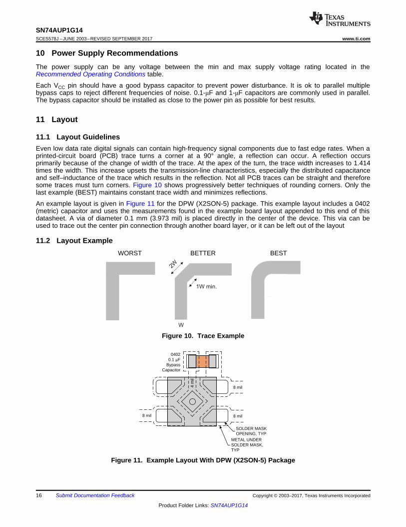
11.1 Layout GuidelinesEven low data rate digital signals can contain high-frequency signal components due to fast edge rates. When aprinted-circuit board (PCB) trace turns a corner at a 90° angle, a reflection can occur. A reflection occursprimarily because of the change of width of the trace. At the apex of the turn, the trace width increases to 1.414times the width. This increase upsets the transmission-line characteristics, especially the distributed capacitanceand self–inductance of the trace which results in the reflection. Not all PCB traces can be straight and thereforesome traces must turn corners. Figure 10 shows progressively better techniques of rounding corners. Only thelast example (BEST) maintains constant trace width and minimizes reflections.
An example layout is given in Figure 11 for the DPW (X2SON-5) package. This example layout includes a 0402(metric) capacitor and uses the measurements found in the example board layout appended to this end of thisdatasheet. A via of diameter 0.1 mm (3.973 mil) is placed directly in the center of the device. This via can beused to trace out the center pin connection through another board layer, or it can be left out of the layout
11.2 Layout Example
Figure 10. Trace Example
Figure 11. Example Layout With DPW (X2SON-5) Package

17
SN74AUP1G14www.ti.com SCES578J –JUNE 2003–REVISED SEPTEMBER 2017
Product Folder Links: SN74AUP1G14
Submit Documentation FeedbackCopyright © 2003–2017, Texas Instruments Incorporated
12 Device and Documentation Support
12.1 Documentation Support
12.1.1 Related DocumentationFor related documentation see the following:
Implications of Slow or Floating CMOS Inputs
12.2 Receiving Notification of Documentation UpdatesTo receive notification of documentation updates, navigate to the device product folder on ti.com. In the upperright corner, click on Alert me to register and receive a weekly digest of any product information that haschanged. For change details, review the revision history included in any revised document.
12.3 Community ResourcesThe following links connect to TI community resources. Linked contents are provided "AS IS" by the respectivecontributors. They do not constitute TI specifications and do not necessarily reflect TI's views; see TI's Terms ofUse.
TI E2E™ Online Community TI's Engineer-to-Engineer (E2E) Community. Created to foster collaborationamong engineers. At e2e.ti.com, you can ask questions, share knowledge, explore ideas and helpsolve problems with fellow engineers.
Design Support TI's Design Support Quickly find helpful E2E forums along with design support tools andcontact information for technical support.
12.4 TrademarksE2E is a trademark of Texas Instruments.All other trademarks are the property of their respective owners.
12.5 Electrostatic Discharge CautionThis integrated circuit can be damaged by ESD. Texas Instruments recommends that all integrated circuits be handled withappropriate precautions. Failure to observe proper handling and installation procedures can cause damage.
ESD damage can range from subtle performance degradation to complete device failure. Precision integrated circuits may be moresusceptible to damage because very small parametric changes could cause the device not to meet its published specifications.
12.6 GlossarySLYZ022 — TI Glossary.
This glossary lists and explains terms, acronyms, and definitions.
13 Mechanical, Packaging, and Orderable InformationThe following pages include mechanical, packaging, and orderable information. This information is the mostcurrent data available for the designated devices. This data is subject to change without notice and revision ofthis document. For browser-based versions of this data sheet, refer to the left-hand navigation.

PACKAGE OPTION ADDENDUM
www.ti.com 24-Aug-2018
Addendum-Page 1
PACKAGING INFORMATION
Orderable Device Status(1)
Package Type PackageDrawing
Pins PackageQty
Eco Plan(2)
Lead/Ball Finish(6)
MSL Peak Temp(3)
Op Temp (°C) Device Marking(4/5)
Samples
SN74AUP1G14DBVR ACTIVE SOT-23 DBV 5 3000 Green (RoHS& no Sb/Br)
CU NIPDAU Level-1-260C-UNLIM -40 to 85 H14R
SN74AUP1G14DBVT ACTIVE SOT-23 DBV 5 250 Green (RoHS& no Sb/Br)
CU NIPDAU Level-1-260C-UNLIM -40 to 85 H14R
SN74AUP1G14DCKR ACTIVE SC70 DCK 5 3000 Green (RoHS& no Sb/Br)
CU NIPDAU Level-1-260C-UNLIM -40 to 85 (HF5, HFF, HFK, HF R)
SN74AUP1G14DCKRG4 ACTIVE SC70 DCK 5 3000 Green (RoHS& no Sb/Br)
CU NIPDAU Level-1-260C-UNLIM -40 to 85 (HF5, HFF, HFK, HF R)
SN74AUP1G14DCKT ACTIVE SC70 DCK 5 250 Green (RoHS& no Sb/Br)
CU NIPDAU Level-1-260C-UNLIM -40 to 85 (HF5, HFK, HFR)
SN74AUP1G14DPWR ACTIVE X2SON DPW 5 3000 Green (RoHS& no Sb/Br)
CU NIPDAU Level-1-260C-UNLIM -40 to 85 BZ
SN74AUP1G14DRLR ACTIVE SOT-5X3 DRL 5 4000 Green (RoHS& no Sb/Br)
CU NIPDAU Level-1-260C-UNLIM -40 to 85 (HF7, HFR)
SN74AUP1G14DRYR ACTIVE SON DRY 6 5000 Green (RoHS& no Sb/Br)
CU NIPDAU Level-1-260C-UNLIM -40 to 85 HF
SN74AUP1G14DSFR ACTIVE SON DSF 6 5000 Green (RoHS& no Sb/Br)
CU NIPDAU |CU NIPDAUAG
Level-1-260C-UNLIM -40 to 85 HF
SN74AUP1G14YFPR ACTIVE DSBGA YFP 4 3000 Green (RoHS& no Sb/Br)
SNAGCU Level-1-260C-UNLIM HFN
(1) The marketing status values are defined as follows:ACTIVE: Product device recommended for new designs.LIFEBUY: TI has announced that the device will be discontinued, and a lifetime-buy period is in effect.NRND: Not recommended for new designs. Device is in production to support existing customers, but TI does not recommend using this part in a new design.PREVIEW: Device has been announced but is not in production. Samples may or may not be available.OBSOLETE: TI has discontinued the production of the device.
(2) RoHS: TI defines "RoHS" to mean semiconductor products that are compliant with the current EU RoHS requirements for all 10 RoHS substances, including the requirement that RoHS substancedo not exceed 0.1% by weight in homogeneous materials. Where designed to be soldered at high temperatures, "RoHS" products are suitable for use in specified lead-free processes. TI mayreference these types of products as "Pb-Free".RoHS Exempt: TI defines "RoHS Exempt" to mean products that contain lead but are compliant with EU RoHS pursuant to a specific EU RoHS exemption.Green: TI defines "Green" to mean the content of Chlorine (Cl) and Bromine (Br) based flame retardants meet JS709B low halogen requirements of <=1000ppm threshold. Antimony trioxide basedflame retardants must also meet the <=1000ppm threshold requirement.
(3) MSL, Peak Temp. - The Moisture Sensitivity Level rating according to the JEDEC industry standard classifications, and peak solder temperature.

PACKAGE OPTION ADDENDUM
www.ti.com 24-Aug-2018
Addendum-Page 2
(4) There may be additional marking, which relates to the logo, the lot trace code information, or the environmental category on the device.
(5) Multiple Device Markings will be inside parentheses. Only one Device Marking contained in parentheses and separated by a "~" will appear on a device. If a line is indented then it is a continuationof the previous line and the two combined represent the entire Device Marking for that device.
(6) Lead/Ball Finish - Orderable Devices may have multiple material finish options. Finish options are separated by a vertical ruled line. Lead/Ball Finish values may wrap to two lines if the finishvalue exceeds the maximum column width.
Important Information and Disclaimer:The information provided on this page represents TI's knowledge and belief as of the date that it is provided. TI bases its knowledge and belief on informationprovided by third parties, and makes no representation or warranty as to the accuracy of such information. Efforts are underway to better integrate information from third parties. TI has taken andcontinues to take reasonable steps to provide representative and accurate information but may not have conducted destructive testing or chemical analysis on incoming materials and chemicals.TI and TI suppliers consider certain information to be proprietary, and thus CAS numbers and other limited information may not be available for release.
In no event shall TI's liability arising out of such information exceed the total purchase price of the TI part(s) at issue in this document sold by TI to Customer on an annual basis.

TAPE AND REEL INFORMATION
*All dimensions are nominal
Device PackageType
PackageDrawing
Pins SPQ ReelDiameter
(mm)
ReelWidth
W1 (mm)
A0(mm)
B0(mm)
K0(mm)
P1(mm)
W(mm)
Pin1Quadrant
SN74AUP1G14DBVR SOT-23 DBV 5 3000 180.0 8.4 3.23 3.17 1.37 4.0 8.0 Q3
SN74AUP1G14DBVT SOT-23 DBV 5 250 180.0 8.4 3.23 3.17 1.37 4.0 8.0 Q3
SN74AUP1G14DCKR SC70 DCK 5 3000 180.0 8.4 2.47 2.3 1.25 4.0 8.0 Q3
SN74AUP1G14DCKR SC70 DCK 5 3000 178.0 9.2 2.4 2.4 1.22 4.0 8.0 Q3
SN74AUP1G14DCKR SC70 DCK 5 3000 180.0 9.2 2.3 2.55 1.2 4.0 8.0 Q3
SN74AUP1G14DCKT SC70 DCK 5 250 178.0 9.2 2.4 2.4 1.22 4.0 8.0 Q3
SN74AUP1G14DCKT SC70 DCK 5 250 180.0 9.2 2.3 2.55 1.2 4.0 8.0 Q3
SN74AUP1G14DPWR X2SON DPW 5 3000 178.0 8.4 0.91 0.91 0.5 2.0 8.0 Q3
SN74AUP1G14DRLR SOT-5X3 DRL 5 4000 180.0 8.4 1.98 1.78 0.69 4.0 8.0 Q3
SN74AUP1G14DRYR SON DRY 6 5000 180.0 9.5 1.15 1.6 0.75 4.0 8.0 Q1
SN74AUP1G14DSFR SON DSF 6 5000 180.0 9.5 1.16 1.16 0.5 4.0 8.0 Q2
SN74AUP1G14YFPR DSBGA YFP 4 3000 178.0 9.2 0.89 0.89 0.58 4.0 8.0 Q1
PACKAGE MATERIALS INFORMATION
www.ti.com 5-Nov-2017
Pack Materials-Page 1
*All dimensions are nominal
Device Package Type Package Drawing Pins SPQ Length (mm) Width (mm) Height (mm)
SN74AUP1G14DBVR SOT-23 DBV 5 3000 202.0 201.0 28.0
SN74AUP1G14DBVT SOT-23 DBV 5 250 202.0 201.0 28.0
SN74AUP1G14DCKR SC70 DCK 5 3000 202.0 201.0 28.0
SN74AUP1G14DCKR SC70 DCK 5 3000 180.0 180.0 18.0
SN74AUP1G14DCKR SC70 DCK 5 3000 205.0 200.0 33.0
SN74AUP1G14DCKT SC70 DCK 5 250 180.0 180.0 18.0
SN74AUP1G14DCKT SC70 DCK 5 250 205.0 200.0 33.0
SN74AUP1G14DPWR X2SON DPW 5 3000 205.0 200.0 33.0
SN74AUP1G14DRLR SOT-5X3 DRL 5 4000 202.0 201.0 28.0
SN74AUP1G14DRYR SON DRY 6 5000 184.0 184.0 19.0
SN74AUP1G14DSFR SON DSF 6 5000 184.0 184.0 19.0
SN74AUP1G14YFPR DSBGA YFP 4 3000 220.0 220.0 35.0
PACKAGE MATERIALS INFORMATION
www.ti.com 5-Nov-2017
Pack Materials-Page 2


GENERIC PACKAGE VIEW
Images above are just a representation of the package family, actual package may vary.Refer to the product data sheet for package details.
DRY 6 USON - 0.6 mm max heightPLASTIC SMALL OUTLINE - NO LEAD
4207181/G

www.ti.com
PACKAGE OUTLINE
C
6X 0.250.15
4X0.5
5X 0.350.25
2X1
0.6 MAX
0.050.00
3X 0.6
0.40.3
B 1.050.95
A
1.51.4
(0.05) TYP (0.127) TYP
4222894/A 01/2018
USON - 0.6 mm max heightDRY0006APLASTIC SMALL OUTLINE - NO LEAD
PIN 1 INDEX AREA
SEATING PLANE
0.08 C
1
34
6
(OPTIONAL)PIN 1 ID
0.1 C A B0.05 C
SYMM
SYMM
NOTES: 1. All linear dimensions are in millimeters. Any dimensions in parenthesis are for reference only. Dimensioning and tolerancing per ASME Y14.5M.2. This drawing is subject to change without notice.
SCALE 8.500
www.ti.com
EXAMPLE BOARD LAYOUT
0.05 MINALL AROUND
0.05 MAXALL AROUND
5X (0.3)
6X (0.2)
4X (0.5)
(0.6)(R0.05) TYP
(0.35)
4222894/A 01/2018
USON - 0.6 mm max heightDRY0006APLASTIC SMALL OUTLINE - NO LEAD
SYMM
1
34
6
SYMM
LAND PATTERN EXAMPLE1:1 RATIO WITH PKG SOLDER PADS
EXPOSED METAL SHOWNSCALE:40X
NOTES: (continued) 3. For more information, see QFN/SON PCB application report in literature No. SLUA271 (www.ti.com/lit/slua271).
METALSOLDER MASKOPENING
SOLDER MASK DETAILS
NON SOLDER MASKDEFINED
EXPOSEDMETAL
SOLDER MASKOPENING
METAL UNDERSOLDER MASK
SOLDER MASKDEFINED
(PREFERRED)
EXPOSEDMETAL

www.ti.com
EXAMPLE STENCIL DESIGN
5X (0.3)
6X (0.2)
4X (0.5)
(0.6)(R0.05) TYP
(0.35)
4222894/A 01/2018
USON - 0.6 mm max heightDRY0006APLASTIC SMALL OUTLINE - NO LEAD
NOTES: (continued) 4. Laser cutting apertures with trapezoidal walls and rounded corners may offer better paste release. IPC-7525 may have alternate design recommendations.
SOLDER PASTE EXAMPLEBASED ON 0.075 - 0.1 mm THICK STENCIL
SCALE:40X
SYMM
1
3 4
6
SYMM

www.ti.com
PACKAGE OUTLINE
C
4X 0.270.17
3X 0.320.23
0.4 MAX
0.050.00
2X0.48
0.270.17
0.25 0.1
B 0.850.75
A
0.850.75
(0.1)
(0.06)
4X (0.05) (0.25)
2X (0.26)
X2SON - 0.4 mm max heightDPW0005APLASTIC SMALL OUTLINE - NO LEAD
4223102/B 09/2017
PIN 1 INDEX AREA
SEATING PLANE
NOTE 3
1
2
3
4
0.1 C A B0.05 C
5
NOTES: 1. All linear dimensions are in millimeters. Any dimensions in parenthesis are for reference only. Dimensioning and tolerancing per ASME Y14.5M. 2. This drawing is subject to change without notice. 3. The size and shape of this feature may vary.
NOTE 3
SCALE 12.000

www.ti.com
EXAMPLE BOARD LAYOUT
0.05 MINALL AROUNDTYP
(0.21) TYPEXPOSED METALCLEARANCE
(0.48)
(0.78)
4X (0.42)
4X (0.22)
( 0.25)
4X (0.26)
4X (0.06)
( 0.1)VIA
(R0.05) TYP
X2SON - 0.4 mm max heightDPW0005APLASTIC SMALL OUTLINE - NO LEAD
4223102/B 09/2017
SYMM
1
2
3
4
SYMM
LAND PATTERN EXAMPLESOLDER MASK DEFINED
SCALE:60X
SOLDER MASKOPENING, TYP
METAL UNDERSOLDER MASKTYP
5
NOTES: (continued) 4. This package is designed to be soldered to a thermal pad on the board. For more information, refer to QFN/SON PCB application note in literature No. SLUA271 (www.ti.com/lit/slua271).

www.ti.com
EXAMPLE STENCIL DESIGN
(0.48)
(0.78)
4X (0.42)
4X (0.22)
4X (0.26)
4X (0.06)
( 0.24)
(0.21)TYP
(R0.05) TYP
X2SON - 0.4 mm max heightDPW0005APLASTIC SMALL OUTLINE - NO LEAD
4223102/B 09/2017
NOTES: (continued) 5. Laser cutting apertures with trapezoidal walls and rounded corners may offer better paste release. IPC-7525 may have alternate design recommendations.
SOLDER PASTE EXAMPLEBASED ON 0.1 mm THICK STENCIL
EXPOSED PAD
92% PRINTED SOLDER COVERAGE BY AREASCALE:100X
SYMM
1
2
3
4
SYMM
EDGESOLDER MASK
5

www.ti.com
PACKAGE OUTLINE
C0.5 MAX
0.190.13
0.4TYP
0.4TYP
4X 0.250.21
B E A
D
4223507/A 01/2017
DSBGA - 0.5 mm max heightYFP0004DIE SIZE BALL GRID ARRAY
NOTES: 1. All linear dimensions are in millimeters. Any dimensions in parenthesis are for reference only. Dimensioning and tolerancing per ASME Y14.5M. 2. This drawing is subject to change without notice.
BALL A1CORNER
SEATING PLANE
BALL TYP 0.05 C
A
B
20.015 C A B
SYMM
SYMM
1
SCALE 10.000
D: Max =
E: Max =
0.79 mm, Min =
0.79 mm, Min =
0.73 mm
0.73 mm

www.ti.com
EXAMPLE BOARD LAYOUT
4X ( 0.23)
(0.4) TYP
(0.4) TYP
( 0.23)METAL
0.05 MAX
SOLDER MASKOPENING
METAL UNDERSOLDER MASK
( 0.23)SOLDER MASKOPENING
0.05 MIN
4223507/A 01/2017
DSBGA - 0.5 mm max heightYFP0004DIE SIZE BALL GRID ARRAY
NOTES: (continued) 3. Final dimensions may vary due to manufacturing tolerance considerations and also routing constraints. For more information, see Texas Instruments literature number SNVA009 (www.ti.com/lit/snva009).
SOLDER MASK DETAILSNOT TO SCALE
SYMM
SYMM
LAND PATTERN EXAMPLEEXPOSED METAL SHOWN
SCALE:50X
A
B
1 2
NON-SOLDER MASKDEFINED
(PREFERRED)
EXPOSEDMETAL
SOLDER MASKDEFINED
EXPOSEDMETAL

www.ti.com
EXAMPLE STENCIL DESIGN
(0.4) TYP
(0.4) TYP
4X ( 0.25) (R0.05) TYP
METALTYP
4223507/A 01/2017
DSBGA - 0.5 mm max heightYFP0004DIE SIZE BALL GRID ARRAY
NOTES: (continued) 4. Laser cutting apertures with trapezoidal walls and rounded corners may offer better paste release.
SYMM
SYMM
SOLDER PASTE EXAMPLEBASED ON 0.1 mm THICK STENCIL
SCALE:50X
A
B
1 2


www.ti.com
PACKAGE OUTLINE
C
TYP0.220.08
0.25
3.02.6
2X 0.95
1.9
1.45 MAX
TYP0.150.00
5X 0.50.3
TYP0.60.3
TYP80
1.9
A
3.052.75
B1.751.45
(1.1)
SOT-23 - 1.45 mm max heightDBV0005ASMALL OUTLINE TRANSISTOR
4214839/C 04/2017
NOTES: 1. All linear dimensions are in millimeters. Any dimensions in parenthesis are for reference only. Dimensioning and tolerancing per ASME Y14.5M.2. This drawing is subject to change without notice.3. Refernce JEDEC MO-178.
0.2 C A B
1
34
5
2
INDEX AREAPIN 1
GAGE PLANE
SEATING PLANE
0.1 C
SCALE 4.000

www.ti.com
EXAMPLE BOARD LAYOUT
0.07 MAXARROUND
0.07 MINARROUND
5X (1.1)
5X (0.6)
(2.6)
(1.9)
2X (0.95)
(R0.05) TYP
4214839/C 04/2017
SOT-23 - 1.45 mm max heightDBV0005ASMALL OUTLINE TRANSISTOR
NOTES: (continued) 4. Publication IPC-7351 may have alternate designs. 5. Solder mask tolerances between and around signal pads can vary based on board fabrication site.
SYMM
LAND PATTERN EXAMPLEEXPOSED METAL SHOWN
SCALE:15X
PKG
1
3 4
5
2
SOLDER MASKOPENINGMETAL UNDER
SOLDER MASK
SOLDER MASKDEFINED
EXPOSED METAL
METALSOLDER MASKOPENING
NON SOLDER MASKDEFINED
(PREFERRED)
SOLDER MASK DETAILS
EXPOSED METAL

www.ti.com
EXAMPLE STENCIL DESIGN
(2.6)
(1.9)
2X(0.95)
5X (1.1)
5X (0.6)
(R0.05) TYP
SOT-23 - 1.45 mm max heightDBV0005ASMALL OUTLINE TRANSISTOR
4214839/C 04/2017
NOTES: (continued) 6. Laser cutting apertures with trapezoidal walls and rounded corners may offer better paste release. IPC-7525 may have alternate design recommendations. 7. Board assembly site may have different recommendations for stencil design.
SOLDER PASTE EXAMPLEBASED ON 0.125 mm THICK STENCIL
SCALE:15X
SYMM
PKG
1
3 4
5
2

www.ti.com
C
6X 0.220.12
6X 0.450.35
2X0.7
4X0.35
0.4 MAX
0.050.00
A 1.050.95 B
1.050.95
(0.11) TYP
(0.1)PIN 1 ID
4208186/F 10/2014
PIN 1 INDEX AREA
SEATING PLANE
0.05 C
1
34
6
0.07 C A B0.05 C
SYMM
SYMM
NOTES: 1. All linear dimensions are in millimeters. Any dimensions in parenthesis are for reference only. Dimensioning and tolerancing per ASME Y14.5M. 2. This drawing is subject to change without notice.3. Reference JEDEC registration MO-287, variation X2AAF.
MECHANICAL DATA
DSF (S-PX2SON-N6) PLASTIC SMALL OUTLINE NO-LEAD

IMPORTANT NOTICE
Texas Instruments Incorporated (TI) reserves the right to make corrections, enhancements, improvements and other changes to itssemiconductor products and services per JESD46, latest issue, and to discontinue any product or service per JESD48, latest issue. Buyersshould obtain the latest relevant information before placing orders and should verify that such information is current and complete.TI’s published terms of sale for semiconductor products (http://www.ti.com/sc/docs/stdterms.htm) apply to the sale of packaged integratedcircuit products that TI has qualified and released to market. Additional terms may apply to the use or sale of other types of TI products andservices.Reproduction of significant portions of TI information in TI data sheets is permissible only if reproduction is without alteration and isaccompanied by all associated warranties, conditions, limitations, and notices. TI is not responsible or liable for such reproduceddocumentation. Information of third parties may be subject to additional restrictions. Resale of TI products or services with statementsdifferent from or beyond the parameters stated by TI for that product or service voids all express and any implied warranties for theassociated TI product or service and is an unfair and deceptive business practice. TI is not responsible or liable for any such statements.Buyers and others who are developing systems that incorporate TI products (collectively, “Designers”) understand and agree that Designersremain responsible for using their independent analysis, evaluation and judgment in designing their applications and that Designers havefull and exclusive responsibility to assure the safety of Designers' applications and compliance of their applications (and of all TI productsused in or for Designers’ applications) with all applicable regulations, laws and other applicable requirements. Designer represents that, withrespect to their applications, Designer has all the necessary expertise to create and implement safeguards that (1) anticipate dangerousconsequences of failures, (2) monitor failures and their consequences, and (3) lessen the likelihood of failures that might cause harm andtake appropriate actions. Designer agrees that prior to using or distributing any applications that include TI products, Designer willthoroughly test such applications and the functionality of such TI products as used in such applications.TI’s provision of technical, application or other design advice, quality characterization, reliability data or other services or information,including, but not limited to, reference designs and materials relating to evaluation modules, (collectively, “TI Resources”) are intended toassist designers who are developing applications that incorporate TI products; by downloading, accessing or using TI Resources in anyway, Designer (individually or, if Designer is acting on behalf of a company, Designer’s company) agrees to use any particular TI Resourcesolely for this purpose and subject to the terms of this Notice.TI’s provision of TI Resources does not expand or otherwise alter TI’s applicable published warranties or warranty disclaimers for TIproducts, and no additional obligations or liabilities arise from TI providing such TI Resources. TI reserves the right to make corrections,enhancements, improvements and other changes to its TI Resources. TI has not conducted any testing other than that specificallydescribed in the published documentation for a particular TI Resource.Designer is authorized to use, copy and modify any individual TI Resource only in connection with the development of applications thatinclude the TI product(s) identified in such TI Resource. NO OTHER LICENSE, EXPRESS OR IMPLIED, BY ESTOPPEL OR OTHERWISETO ANY OTHER TI INTELLECTUAL PROPERTY RIGHT, AND NO LICENSE TO ANY TECHNOLOGY OR INTELLECTUAL PROPERTYRIGHT OF TI OR ANY THIRD PARTY IS GRANTED HEREIN, including but not limited to any patent right, copyright, mask work right, orother intellectual property right relating to any combination, machine, or process in which TI products or services are used. Informationregarding or referencing third-party products or services does not constitute a license to use such products or services, or a warranty orendorsement thereof. Use of TI Resources may require a license from a third party under the patents or other intellectual property of thethird party, or a license from TI under the patents or other intellectual property of TI.TI RESOURCES ARE PROVIDED “AS IS” AND WITH ALL FAULTS. TI DISCLAIMS ALL OTHER WARRANTIES ORREPRESENTATIONS, EXPRESS OR IMPLIED, REGARDING RESOURCES OR USE THEREOF, INCLUDING BUT NOT LIMITED TOACCURACY OR COMPLETENESS, TITLE, ANY EPIDEMIC FAILURE WARRANTY AND ANY IMPLIED WARRANTIES OFMERCHANTABILITY, FITNESS FOR A PARTICULAR PURPOSE, AND NON-INFRINGEMENT OF ANY THIRD PARTY INTELLECTUALPROPERTY RIGHTS. TI SHALL NOT BE LIABLE FOR AND SHALL NOT DEFEND OR INDEMNIFY DESIGNER AGAINST ANY CLAIM,INCLUDING BUT NOT LIMITED TO ANY INFRINGEMENT CLAIM THAT RELATES TO OR IS BASED ON ANY COMBINATION OFPRODUCTS EVEN IF DESCRIBED IN TI RESOURCES OR OTHERWISE. IN NO EVENT SHALL TI BE LIABLE FOR ANY ACTUAL,DIRECT, SPECIAL, COLLATERAL, INDIRECT, PUNITIVE, INCIDENTAL, CONSEQUENTIAL OR EXEMPLARY DAMAGES INCONNECTION WITH OR ARISING OUT OF TI RESOURCES OR USE THEREOF, AND REGARDLESS OF WHETHER TI HAS BEENADVISED OF THE POSSIBILITY OF SUCH DAMAGES.Unless TI has explicitly designated an individual product as meeting the requirements of a particular industry standard (e.g., ISO/TS 16949and ISO 26262), TI is not responsible for any failure to meet such industry standard requirements.Where TI specifically promotes products as facilitating functional safety or as compliant with industry functional safety standards, suchproducts are intended to help enable customers to design and create their own applications that meet applicable functional safety standardsand requirements. Using products in an application does not by itself establish any safety features in the application. Designers mustensure compliance with safety-related requirements and standards applicable to their applications. Designer may not use any TI products inlife-critical medical equipment unless authorized officers of the parties have executed a special contract specifically governing such use.Life-critical medical equipment is medical equipment where failure of such equipment would cause serious bodily injury or death (e.g., lifesupport, pacemakers, defibrillators, heart pumps, neurostimulators, and implantables). Such equipment includes, without limitation, allmedical devices identified by the U.S. Food and Drug Administration as Class III devices and equivalent classifications outside the U.S.TI may expressly designate certain products as completing a particular qualification (e.g., Q100, Military Grade, or Enhanced Product).Designers agree that it has the necessary expertise to select the product with the appropriate qualification designation for their applicationsand that proper product selection is at Designers’ own risk. Designers are solely responsible for compliance with all legal and regulatoryrequirements in connection with such selection.Designer will fully indemnify TI and its representatives against any damages, costs, losses, and/or liabilities arising out of Designer’s non-compliance with the terms and provisions of this Notice.
Mailing Address: Texas Instruments, Post Office Box 655303, Dallas, Texas 75265Copyright © 2018, Texas Instruments Incorporated