Embed Size (px)
Citation preview
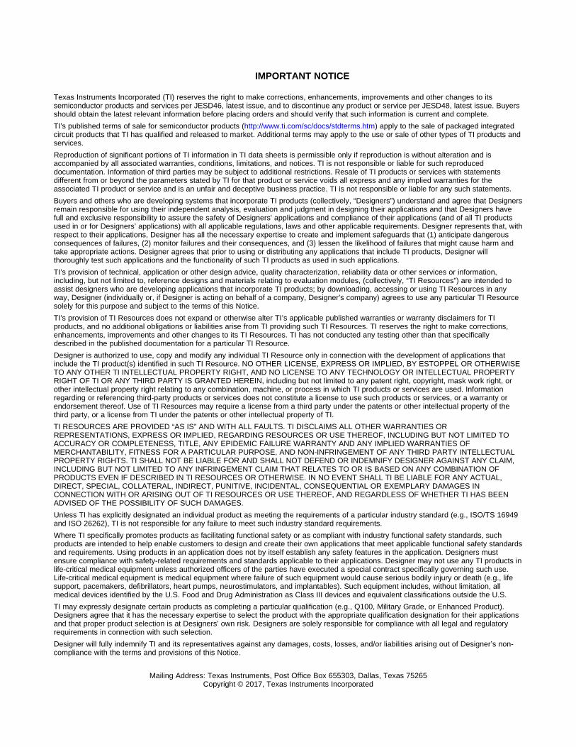
0 V ±250 mV
2.55 V ±2 V
1.29 V ±2 V
VDD2 = 5 V
VDD2 = 3.3 V
GND1 GND2
VDD1 VDD2
VOUTP
VOUTN
VINP
VINN
Product
Folder
Sample &Buy
Technical
Documents
Tools &
Software
Support &Community
ReferenceDesign
An IMPORTANT NOTICE at the end of this data sheet addresses availability, warranty, changes, use in safety-critical applications,intellectual property matters and other important disclaimers. PRODUCTION DATA.
AMC1200-Q1SBAS585A –SEPTEMBER 2012–REVISED JANUARY 2016
AMC1200-Q1 Fully-Differential Isolation Amplifier
1
1 Features1• Qualified for Automotive Applications• AEC-Q100 Qualified With the Following Results:
– Temperature Grade 2: –40°C to 105°C– HBM ESD Classification Level H2– CDM ESD Classification Level C3B
• ±250-mV Input Voltage Range Optimized forShunt Resistors
• Very Low Nonlinearity: 0.075% (max)with 5-V High-Side Supply
• Low Offset Error: 1.5 mV (max)• Low Noise: 3.1 mVRMS (typical)• Low High-Side Supply Current:
8 mA (max) at 5 V• Input Bandwidth: 60 kHz (min)• Fixed Gain: 8 (0.5% accuracy)• High Common-Mode Rejection Ratio:
108 dB (typical)• 3.3-V Operation on Low-Side• Certified Galvanic Isolation:
– UL1577 and VDE V 0884-10 Approved– Isolation Voltage: 4250 VPEAK
– Working Voltage: 1200 VPEAK
– Transient Immunity: 10 kV/µs (min)• Typical 10-Year Lifespan at Rated Working
Voltage (see Application Report, SLLA197)
2 Applications• Isolated Shunt-Resistor-Based Current or Voltage
Sensing in:– Traction Inverters– On-Board Chargers– DC-DC Converters– Battery Management Systems
3 DescriptionThe AMC1200-Q1 is a precision isolation amplifierwith the output separated from the input circuitry by asilicon dioxide (SiO2) barrier that is highly resistant tomagnetic interference. This barrier is certified toprovide galvanic isolation of up to 4250 VPEAKaccording to UL1577 and VDE V 0884-10. Used inconjunction with isolated power supplies, this deviceprevents noise currents on a high common-modevoltage line from entering the local ground andinterfering with or damaging sensitive circuitry.
The input of the AMC1200-Q1 is optimized for directconnection to shunt resistors or other low-voltagelevel signal sources. The performance of the devicesupports accurate current control, resulting in system-level power saving and (especially in motor-controlapplications) lower torque ripple. The common-modevoltage of the output signal is automatically adjustedto either the 3-V or 5-V low-side supply.
The AMC1200-Q1 is available in a wide-body, 8-pinSOIC package (DWV) and a gullwing, 8-pin SOPpackage (DUB).
Device Information(1)
PART NUMBER PACKAGE BODY SIZE (NOM)
AMC1200-Q1SOP (8) 9.50 mm × 6.62 mmSOIC (8) 5.85 mm × 7.50 mm
(1) For all available packages, see the orderable addendum atthe end of the data sheet.
Simplified Schematic
2
AMC1200-Q1SBAS585A –SEPTEMBER 2012–REVISED JANUARY 2016 www.ti.com
Product Folder Links: AMC1200-Q1
Submit Documentation Feedback Copyright © 2012–2016, Texas Instruments Incorporated
Table of Contents1 Features .................................................................. 12 Applications ........................................................... 13 Description ............................................................. 14 Revision History..................................................... 25 Pin Configurations and Functions ....................... 36 Specifications......................................................... 4
6.1 Absolute Maximum Ratings ..................................... 46.2 ESD Ratings.............................................................. 46.3 Recommended Operating Conditions....................... 46.4 Thermal Information .................................................. 46.5 Electrical Characteristics........................................... 56.6 Typical Characteristics .............................................. 6
7 Detailed Description ............................................ 117.1 Overview ................................................................. 117.2 Functional Block Diagram ....................................... 117.3 Feature Description................................................. 12
7.4 Device Functional Modes........................................ 148 Application and Implementation ........................ 15
8.1 Application Information............................................ 158.2 Typical Applications ................................................ 15
9 Power Supply Recommendations ...................... 1810 Layout................................................................... 19
10.1 Layout Guidelines ................................................. 1910.2 Layout Example .................................................... 19
11 Device and Documentation Support ................. 2011.1 Documentation Support ........................................ 2011.2 Community Resources.......................................... 2011.3 Trademarks ........................................................... 2011.4 Electrostatic Discharge Caution............................ 2011.5 Glossary ................................................................ 20
12 Mechanical, Packaging, and OrderableInformation ........................................................... 20
4 Revision HistoryNOTE: Page numbers for previous revisions may differ from page numbers in the current version.
Changes from Original (September 2012) to Revision A Page
• Deleted last Features bullet ................................................................................................................................................... 1• Added front-page image caption, ESD Ratings table, Feature Description section, Device Functional Modes section,
Application and Implementation section, Power Supply Recommendations section, Layout section, Device andDocumentation Support section, and Mechanical, Packaging, and Orderable Information section....................................... 1
• Added TI Design .................................................................................................................................................................... 1• Changed front-page graphic .................................................................................................................................................. 1• Changed Pin Configurations and Functions section: condensed pin out drawing into one because packages have
identical pin layout ................................................................................................................................................................. 3• Moved Electrical Characteristics table before Regulatory Information table to comply with latest format ............................ 5• Added PSRR to test conditions of Output, PSRR parameter in Electrical Characteristics table .......................................... 5• Changed CTI parameter in Package Characteristics table: added DWV package row ...................................................... 13• Added sentence to Design Requirements section .............................................................................................................. 16
1
2
3
4
8
7
6
5
VDD2
VOUTP
VOUTN
GND2
VDD1
VINP
VINN
GND1
3
AMC1200-Q1www.ti.com SBAS585A –SEPTEMBER 2012–REVISED JANUARY 2016
Product Folder Links: AMC1200-Q1
Submit Documentation FeedbackCopyright © 2012–2016, Texas Instruments Incorporated
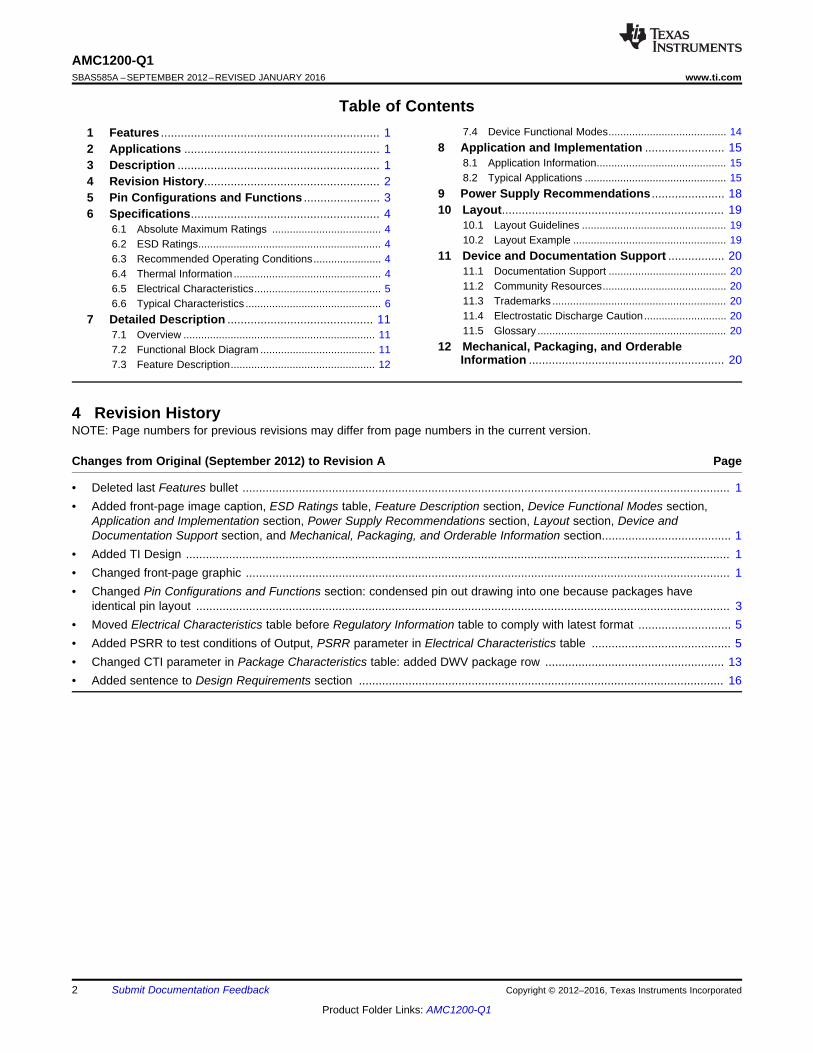
5 Pin Configurations and Functions
DUB and DWV Packages8-Pin SOP and SOIC
Top View
Pin FunctionsPIN
I/O DESCRIPTIONNO. NAME
1 VDD1 — High-side power supply, 4.5 V to 5.5 V.See the Power Supply Recommendations section for decoupling recommendations.
2 VINP I Noninverting analog input3 VINN I Inverting analog input4 GND1 — High-side analog ground5 GND2 — Low-side analog ground6 VOUTN O Inverting analog output with self-adjusting, common-mode voltage7 VOUTP O Noninverting analog output with self-adjusting, common-mode voltage
8 VDD2 — Low-side power supply, 2.7 V to 5.5 V.See the Power Supply Recommendations section for decoupling recommendations.
4
AMC1200-Q1SBAS585A –SEPTEMBER 2012–REVISED JANUARY 2016 www.ti.com
Product Folder Links: AMC1200-Q1
Submit Documentation Feedback Copyright © 2012–2016, Texas Instruments Incorporated
(1) Stresses beyond those listed under Absolute Maximum Ratings may cause permanent damage to the device. These are stress ratingsonly, and functional operation of the device at these or any other conditions beyond those indicated is not implied. Exposure to absolutemaximum rated conditions for extended periods may affect device reliability.
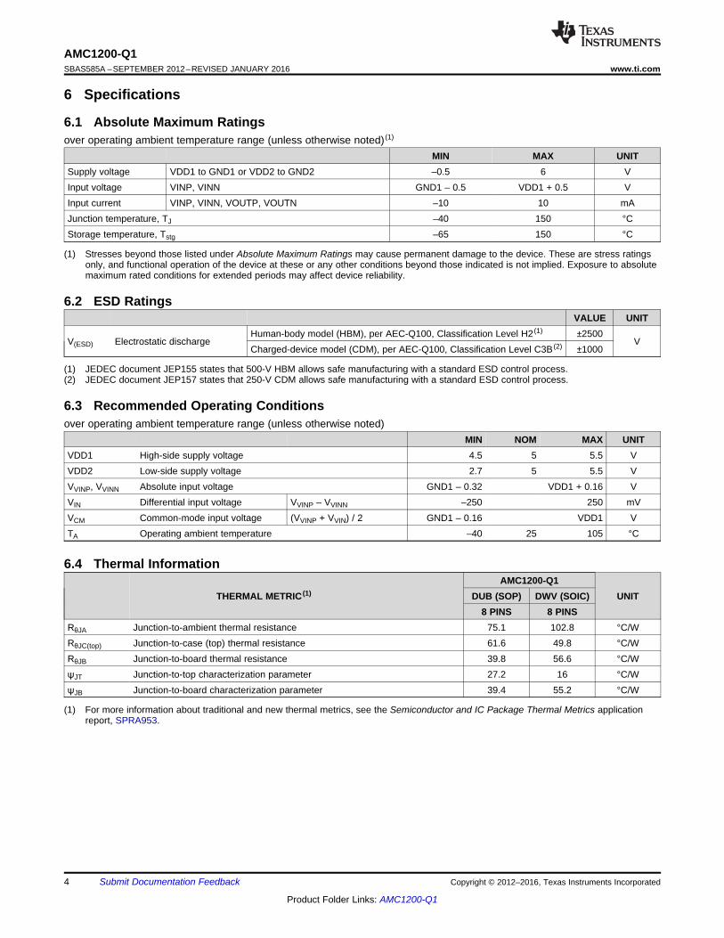
6 Specifications
6.1 Absolute Maximum Ratingsover operating ambient temperature range (unless otherwise noted) (1)
MIN MAX UNITSupply voltage VDD1 to GND1 or VDD2 to GND2 –0.5 6 VInput voltage VINP, VINN GND1 – 0.5 VDD1 + 0.5 VInput current VINP, VINN, VOUTP, VOUTN –10 10 mAJunction temperature, TJ –40 150 °CStorage temperature, Tstg –65 150 °C
(1) JEDEC document JEP155 states that 500-V HBM allows safe manufacturing with a standard ESD control process.(2) JEDEC document JEP157 states that 250-V CDM allows safe manufacturing with a standard ESD control process.
6.2 ESD RatingsVALUE UNIT
V(ESD) Electrostatic dischargeHuman-body model (HBM), per AEC-Q100, Classification Level H2 (1) ±2500
VCharged-device model (CDM), per AEC-Q100, Classification Level C3B (2) ±1000
6.3 Recommended Operating Conditionsover operating ambient temperature range (unless otherwise noted)
MIN NOM MAX UNITVDD1 High-side supply voltage 4.5 5 5.5 VVDD2 Low-side supply voltage 2.7 5 5.5 VVVINP, VVINN Absolute input voltage GND1 – 0.32 VDD1 + 0.16 VVIN Differential input voltage VVINP – VVINN –250 250 mVVCM Common-mode input voltage (VVINP + VVIN) / 2 GND1 – 0.16 VDD1 VTA Operating ambient temperature –40 25 105 °C
(1) For more information about traditional and new thermal metrics, see the Semiconductor and IC Package Thermal Metrics applicationreport, SPRA953.
6.4 Thermal Information
THERMAL METRIC (1)AMC1200-Q1
UNITDUB (SOP) DWV (SOIC)8 PINS 8 PINS
RθJA Junction-to-ambient thermal resistance 75.1 102.8 °C/WRθJC(top) Junction-to-case (top) thermal resistance 61.6 49.8 °C/WRθJB Junction-to-board thermal resistance 39.8 56.6 °C/WψJT Junction-to-top characterization parameter 27.2 16 °C/WψJB Junction-to-board characterization parameter 39.4 55.2 °C/W
5
AMC1200-Q1www.ti.com SBAS585A –SEPTEMBER 2012–REVISED JANUARY 2016
Product Folder Links: AMC1200-Q1
Submit Documentation FeedbackCopyright © 2012–2016, Texas Instruments Incorporated
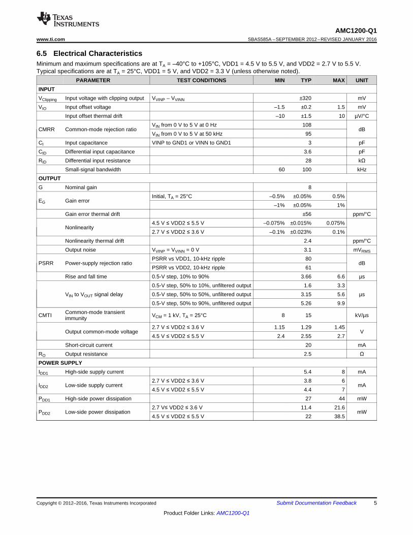
6.5 Electrical CharacteristicsMinimum and maximum specifications are at TA = –40°C to +105°C, VDD1 = 4.5 V to 5.5 V, and VDD2 = 2.7 V to 5.5 V.Typical specifications are at TA = 25°C, VDD1 = 5 V, and VDD2 = 3.3 V (unless otherwise noted).
PARAMETER TEST CONDITIONS MIN TYP MAX UNITINPUTVClipping Input voltage with clipping output VVINP – VVINN ±320 mVVIO Input offset voltage –1.5 ±0.2 1.5 mV
Input offset thermal drift –10 ±1.5 10 µV/°C
CMRR Common-mode rejection ratioVIN from 0 V to 5 V at 0 Hz 108
dBVIN from 0 V to 5 V at 50 kHz 95
CI Input capacitance VINP to GND1 or VINN to GND1 3 pFCID Differential input capacitance 3.6 pFRID Differential input resistance 28 kΩ
Small-signal bandwidth 60 100 kHzOUTPUTG Nominal gain 8
EG Gain errorInitial, TA = 25°C –0.5% ±0.05% 0.5%
–1% ±0.05% 1%Gain error thermal drift ±56 ppm/°C
Nonlinearity4.5 V ≤ VDD2 ≤ 5.5 V –0.075% ±0.015% 0.075%2.7 V ≤ VDD2 ≤ 3.6 V –0.1% ±0.023% 0.1%
Nonlinearity thermal drift 2.4 ppm/°COutput noise VVINP = VVINN = 0 V 3.1 mVRMS
PSRR Power-supply rejection ratioPSRR vs VDD1, 10-kHz ripple 80
dBPSRR vs VDD2, 10-kHz ripple 61
Rise and fall time 0.5-V step, 10% to 90% 3.66 6.6 µs
VIN to VOUT signal delay0.5-V step, 50% to 10%, unfiltered output 1.6 3.3
µs0.5-V step, 50% to 50%, unfiltered output 3.15 5.60.5-V step, 50% to 90%, unfiltered output 5.26 9.9
CMTI Common-mode transientimmunity VCM = 1 kV, TA = 25°C 8 15 kV/µs
Output common-mode voltage2.7 V ≤ VDD2 ≤ 3.6 V 1.15 1.29 1.45
V4.5 V ≤ VDD2 ≤ 5.5 V 2.4 2.55 2.7
Short-circuit current 20 mARO Output resistance 2.5 ΩPOWER SUPPLYIDD1 High-side supply current 5.4 8 mA
IDD2 Low-side supply current2.7 V ≤ VDD2 ≤ 3.6 V 3.8 6
mA4.5 V ≤ VDD2 ≤ 5.5 V 4.4 7
PDD1 High-side power dissipation 27 44 mW
PDD2 Low-side power dissipation2.7 V≤ VDD2 ≤ 3.6 V 11.4 21.6
mW4.5 V ≤ VDD2 ≤ 5.5 V 22 38.5
50
60
70
80
90
100
110
120
130
0.1 1 10 100Input Frequency (kHz)
CM
RR
(dB
)
−40
−30
−20
−10
0
10
20
30
40
−400 −300 −200 −100 0 100 200 300 400Input Voltage (mV)
Inpu
t Cur
rent
(µA
)
−2
−1.5
−1
−0.5
0
0.5
1
1.5
2
4.5 4.75 5 5.25 5.5VDD2 (V)
Inpu
t Offs
et (
mV
)
VDD2 = 4.5 V to 5.5 V
−2
−1.5
−1
−0.5
0
0.5
1
1.5
2
−40 −25 −10 5 20 35 50 65 80 95 110 125Temperature (°C)
Inpu
t Offs
et (
mV
)
−2
−1.5
−1
−0.5
0
0.5
1
1.5
2
4.5 4.75 5 5.25 5.5VDD1 (V)
Inpu
t Offs
et (
mV
)
−2
−1.5
−1
−0.5
0
0.5
1
1.5
2
2.7 3 3.3 3.6VDD2 (V)
Inpu
t Offs
et (
mV
)
VDD2 = 2.7 V to 3.6 V
6
AMC1200-Q1SBAS585A –SEPTEMBER 2012–REVISED JANUARY 2016 www.ti.com
Product Folder Links: AMC1200-Q1
Submit Documentation Feedback Copyright © 2012–2016, Texas Instruments Incorporated
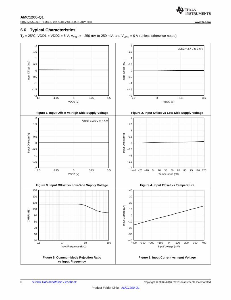
6.6 Typical CharacteristicsTA = 25°C, VDD1 = VDD2 = 5 V, VVINP = –250 mV to 250 mV, and VVINN = 0 V (unless otherwise noted)
Figure 1. Input Offset vs High-Side Supply Voltage Figure 2. Input Offset vs Low-Side Supply Voltage
Figure 3. Input Offset vs Low-Side Supply Voltage Figure 4. Input Offset vs Temperature
Figure 5. Common-Mode Rejection Ratiovs Input Frequency
Figure 6. Input Current vs Input Voltage
−1
−0.8
−0.6
−0.4
−0.2
0
0.2
0.4
0.6
0.8
1
−40 −25 −10 5 20 35 50 65 80 95 110 125Temperature (°C)
Gai
n E
rror
(%
)
−80
−70
−60
−50
−40
−30
−20
−10
0
10
1 10 100 500Input Frequency (kHz)
Nor
mal
ized
Gai
n (d
B)
−1
−0.8
−0.6
−0.4
−0.2
0
0.2
0.4
0.6
0.8
1
2.7 3 3.3 3.6VDD2 (V)
Gai
n E
rror
(%
)
VDD2 = 2.7 V to 3.6 V
−1
−0.8
−0.6
−0.4
−0.2
0
0.2
0.4
0.6
0.8
1
4.5 4.75 5 5.25 5.5VDD2 (V)
Gai
n E
rror
(%
)
VDD2 = 4.5 V to 5.5 V
60
70
80
90
100
110
120
−40 −25 −10 5 20 35 50 65 80 95 110 125Temperature (°C)
Inpu
t Ban
dwid
th (
kHz)
−1
−0.8
−0.6
−0.4
−0.2
0
0.2
0.4
0.6
0.8
1
4.5 4.75 5 5.25 5.5VDD1 (V)
Gai
n E
rror
(%
)
7
AMC1200-Q1www.ti.com SBAS585A –SEPTEMBER 2012–REVISED JANUARY 2016
Product Folder Links: AMC1200-Q1
Submit Documentation FeedbackCopyright © 2012–2016, Texas Instruments Incorporated
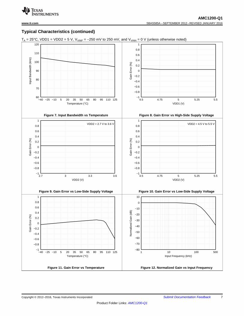
Typical Characteristics (continued)TA = 25°C, VDD1 = VDD2 = 5 V, VVINP = –250 mV to 250 mV, and VVINN = 0 V (unless otherwise noted)
Figure 7. Input Bandwidth vs Temperature Figure 8. Gain Error vs High-Side Supply Voltage
Figure 9. Gain Error vs Low-Side Supply Voltage Figure 10. Gain Error vs Low-Side Supply Voltage
Figure 11. Gain Error vs Temperature Figure 12. Normalized Gain vs Input Frequency
−0.1
−0.08
−0.06
−0.04
−0.02
0
0.02
0.04
0.06
0.08
0.1
2.7 3 3.3 3.6VDD2 (V)
Non
linea
rity
(%)
VDD2 = 2.7 V to 3.6 V
−0.1
−0.08
−0.06
−0.04
−0.02
0
0.02
0.04
0.06
0.08
0.1
4.5 4.75 5 5.25 5.5VDD2 (V)
Non
linea
rity
(%)
VDD2 = 4.5 V to 5.5 V
0
0.3
0.6
0.9
1.2
1.5
1.8
2.1
2.4
2.7
3
3.3
3.6
−400 −300 −200 −100 0 100 200 300 400Input Voltage (mV)
Out
put V
olta
ge (
V)
VOUTPVOUTN
VDD2 = 2.7 V to 3.6 V
−0.1
−0.08
−0.06
−0.04
−0.02
0
0.02
0.04
0.06
0.08
0.1
4.5 4.75 5 5.25 5.5VDD1 (V)
Non
linea
rity
(%)
−360
−330
−300
−270
−240
−210
−180
−150
−120
−90
−60
−30
0
1 10 100 1000Input Frequency (kHz)
Out
put P
hase
(°)
0
0.5
1
1.5
2
2.5
3
3.5
4
4.5
5
−400 −300 −200 −100 0 100 200 300 400Input Voltage (mV)
Out
put V
olta
ge (
V)
VOUTPVOUTN
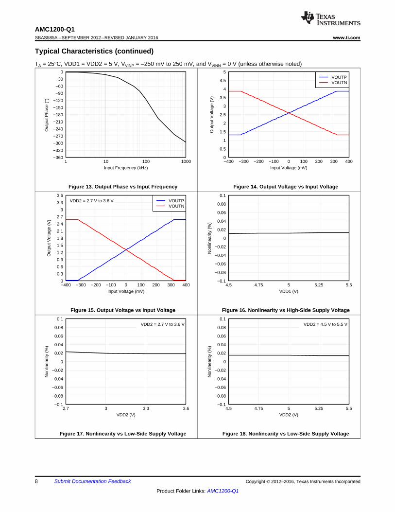
8
AMC1200-Q1SBAS585A –SEPTEMBER 2012–REVISED JANUARY 2016 www.ti.com
Product Folder Links: AMC1200-Q1
Submit Documentation Feedback Copyright © 2012–2016, Texas Instruments Incorporated
Typical Characteristics (continued)TA = 25°C, VDD1 = VDD2 = 5 V, VVINP = –250 mV to 250 mV, and VVINN = 0 V (unless otherwise noted)
Figure 13. Output Phase vs Input Frequency Figure 14. Output Voltage vs Input Voltage
Figure 15. Output Voltage vs Input Voltage Figure 16. Nonlinearity vs High-Side Supply Voltage
Figure 17. Nonlinearity vs Low-Side Supply Voltage Figure 18. Nonlinearity vs Low-Side Supply Voltage
0
1
2
3
4
5
6
7
8
9
10
−40 −25 −10 5 20 35 50 65 80 95 110 125Temperature (°C)
Out
put R
ise/
Fal
l Tim
e (µ
s)
Time (2 s/div)m
200 mV/div
500 mV/div
500 mV/div
600
800
1000
1200
1400
1600
1800
2000
2200
2400
2600
0.1 1 10 100Frequency (kHz)
Noi
se (
nV/s
qrt(
Hz)
)
0
10
20
30
40
50
60
70
80
90
100
1 10 100Ripple Frequency (kHz)
PS
RR
(dB
)
VDD1VDD2
−0.1
−0.08
−0.06
−0.04
−0.02
0
0.02
0.04
0.06
0.08
0.1
−250 −200 −150 −100 −50 0 50 100 150 200 250Input Voltage (mV)
Non
linea
rity
(%)
VDD2 = 3 VVDD2 = 5 V
−0.1
−0.08
−0.06
−0.04
−0.02
0
0.02
0.04
0.06
0.08
0.1
−40 −25 −10 5 20 35 50 65 80 95 110 125Temperature (°C)
Non
linea
rity
(%)
9
AMC1200-Q1www.ti.com SBAS585A –SEPTEMBER 2012–REVISED JANUARY 2016
Product Folder Links: AMC1200-Q1
Submit Documentation FeedbackCopyright © 2012–2016, Texas Instruments Incorporated
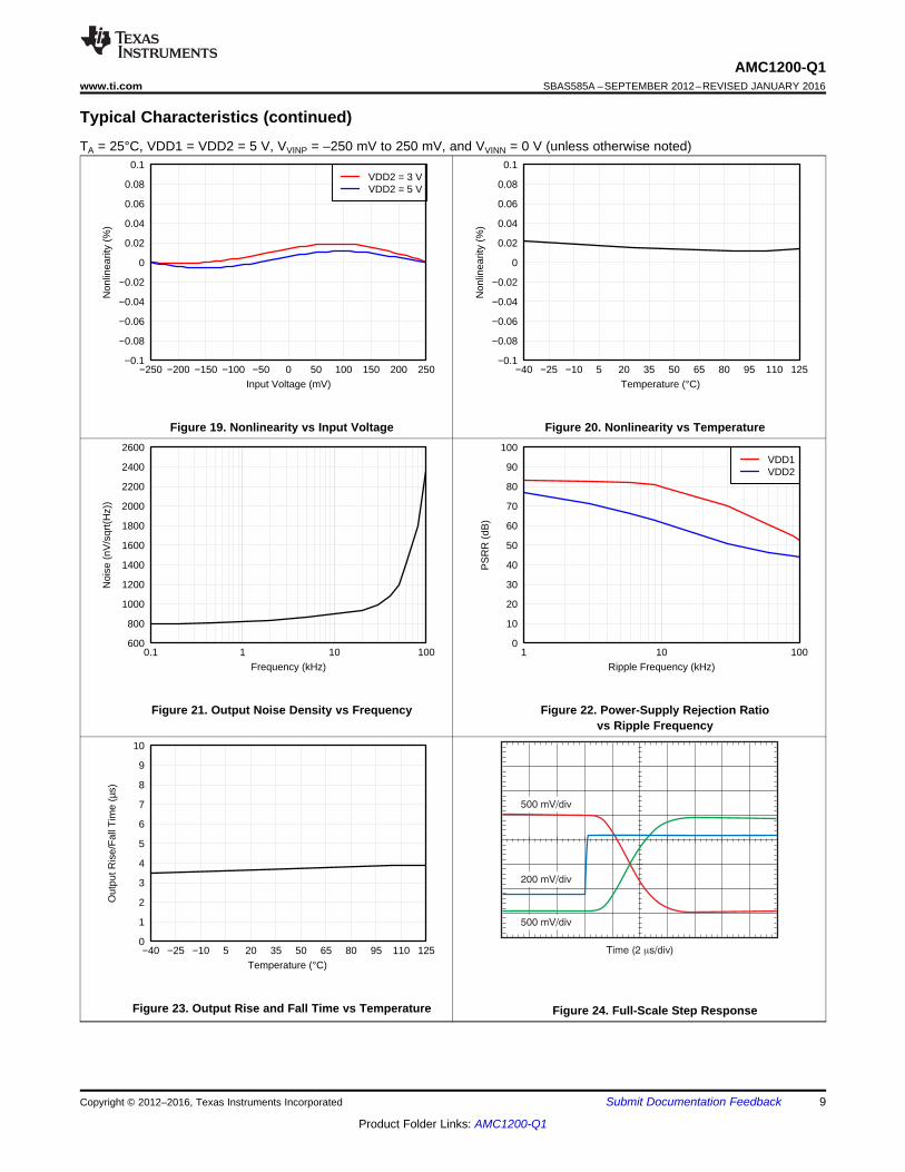
Typical Characteristics (continued)TA = 25°C, VDD1 = VDD2 = 5 V, VVINP = –250 mV to 250 mV, and VVINN = 0 V (unless otherwise noted)
Figure 19. Nonlinearity vs Input Voltage Figure 20. Nonlinearity vs Temperature
Figure 21. Output Noise Density vs Frequency Figure 22. Power-Supply Rejection Ratiovs Ripple Frequency
Figure 23. Output Rise and Fall Time vs Temperature Figure 24. Full-Scale Step Response
0
1
2
3
4
5
6
7
8
2.7 3 3.3 3.6VDD2 (V)
IDD
2 (m
A)
VDD2 = 2.7 V to 3.6 V
0
1
2
3
4
5
6
7
8
−40 −25 −10 5 20 35 50 65 80 95 110 125Temperature (°C)
Sup
ply
Cur
rent
(m
A)
IDD1IDD2
0
1
2
3
4
5
−40 −25 −10 5 20 35 50 65 80 95 110 125Temperature (°C)
Out
put C
omm
on−
Mod
e V
olta
ge (
V) VDD2 = 2.7 V to 3.6 V
VDD2 = 4.5 V to 5.5 V
0
1
2
3
4
5
6
7
8
4.5 4.75 5 5.25 5.5Supply Voltage (V)
Sup
ply
Cur
rent
(m
A)
IDD1IDD2
0
1
2
3
4
5
6
7
8
9
10
−40 −25 −10 5 20 35 50 65 80 95 110 125Temperature (°C)
Sig
nal D
elay
(µs
)
50% to 10%50% to 50%50% to 90%
0
1
2
3
4
5
3.5 3.6 3.7 3.8 3.9 4 4.1 4.2 4.3 4.4 4.5VDD2 (V)
Out
put C
omm
on−
Mod
e V
olta
ge (
V) VDD2 rising
VDD2 falling
10
AMC1200-Q1SBAS585A –SEPTEMBER 2012–REVISED JANUARY 2016 www.ti.com
Product Folder Links: AMC1200-Q1
Submit Documentation Feedback Copyright © 2012–2016, Texas Instruments Incorporated
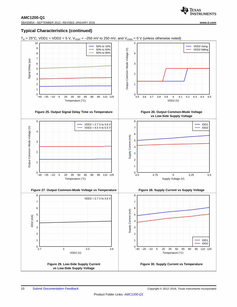
Typical Characteristics (continued)TA = 25°C, VDD1 = VDD2 = 5 V, VVINP = –250 mV to 250 mV, and VVINN = 0 V (unless otherwise noted)
Figure 25. Output Signal Delay Time vs Temperature Figure 26. Output Common-Mode Voltagevs Low-Side Supply Voltage
Figure 27. Output Common-Mode Voltage vs Temperature Figure 28. Supply Current vs Supply Voltage
Figure 29. Low-Side Supply Currentvs Low-Side Supply Voltage
Figure 30. Supply Current vs Temperature
IsolationBarrier
ûModulator
RX
2.5-VReference
VOUTP
VOUTN
VDD2
GND2GND1
VINP
VINN
VDD1
RC Oscillator
RX
TX
TX
Retiming and 3rd-Order
Active Low-Pass
Filter
DATA
CLK
2.56-VReference
11
AMC1200-Q1www.ti.com SBAS585A –SEPTEMBER 2012–REVISED JANUARY 2016
Product Folder Links: AMC1200-Q1
Submit Documentation FeedbackCopyright © 2012–2016, Texas Instruments Incorporated
7 Detailed Description
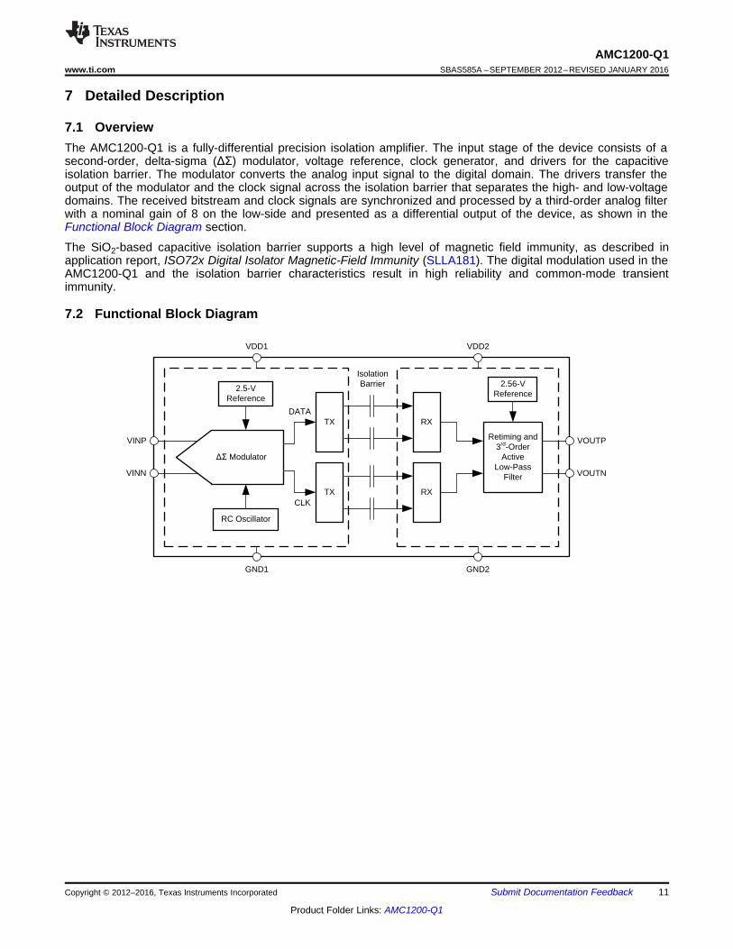
7.1 OverviewThe AMC1200-Q1 is a fully-differential precision isolation amplifier. The input stage of the device consists of asecond-order, delta-sigma (ΔΣ) modulator, voltage reference, clock generator, and drivers for the capacitiveisolation barrier. The modulator converts the analog input signal to the digital domain. The drivers transfer theoutput of the modulator and the clock signal across the isolation barrier that separates the high- and low-voltagedomains. The received bitstream and clock signals are synchronized and processed by a third-order analog filterwith a nominal gain of 8 on the low-side and presented as a differential output of the device, as shown in theFunctional Block Diagram section.
The SiO2-based capacitive isolation barrier supports a high level of magnetic field immunity, as described inapplication report, ISO72x Digital Isolator Magnetic-Field Immunity (SLLA181). The digital modulation used in theAMC1200-Q1 and the isolation barrier characteristics result in high reliability and common-mode transientimmunity.
7.2 Functional Block Diagram
12
AMC1200-Q1SBAS585A –SEPTEMBER 2012–REVISED JANUARY 2016 www.ti.com
Product Folder Links: AMC1200-Q1
Submit Documentation Feedback Copyright © 2012–2016, Texas Instruments Incorporated
7.3 Feature Description
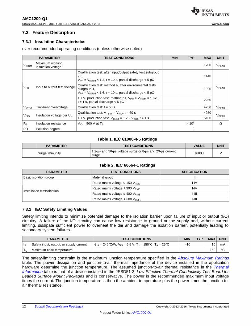
7.3.1 Insulation Characteristicsover recommended operating conditions (unless otherwise noted)
PARAMETER TEST CONDITIONS MIN TYP MAX UNIT
VIORMMaximum workinginsulation voltage 1200 VPEAK
VPR Input to output test voltage
Qualification test: after input/output safety test subgroup2/3,VPR = VIORM × 1.2, t = 10 s, partial discharge < 5 pC
1440
VPEAKQualification test: method a, after environmental testssubgroup 1,VPR = VIORM × 1.6, t = 10 s, partial discharge < 5 pC
1920
100% production test: method b1, VPR = VIORM × 1.875,t = 1 s, partial discharge < 5 pC 2250
VIOTM Transient overvoltage Qualification test: t = 60 s 4250 VPEAK
VISO Insulation voltage per ULQualification test: VTEST = VISO, t = 60 s 4250
VPEAK100% production test: VTEST = 1.2 × VISO, t = 1 s 5100RS Insulation resistance VIO = 500 V at TS > 109 ΩPD Pollution degree 2
Table 1. IEC 61000-4-5 RatingsPARAMETER TEST CONDITIONS VALUE UNIT
Surge immunity 1.2-μs and 50-μs voltage surge or 8-μs and 20-μs currentsurge ±6000 V
Table 2. IEC 60664-1 RatingsPARAMETER TEST CONDITIONS SPECIFICATION
Basic isolation group Material group II
Installation classification
Rated mains voltage ≤ 150 VRMS I-IVRated mains voltage ≤ 300 VRMS I-IVRated mains voltage ≤ 400 VRMS I-IIIRated mains voltage < 600 VRMS I-III
7.3.2 IEC Safety Limiting ValuesSafety limiting intends to minimize potential damage to the isolation barrier upon failure of input or output (I/O)circuitry. A failure of the I/O circuitry can cause low resistance to ground or the supply and, without currentlimiting, dissipate sufficient power to overheat the die and damage the isolation barrier, potentially leading tosecondary system failures.
PARAMETER TEST CONDITIONS MIN TYP MAX UNITIS Safety input, output, or supply current θJA = 246°C/W, VIN = 5.5 V, TJ = 150°C, TA = 25°C –10 10 mATC Maximum case temperature 150 °C
The safety-limiting constraint is the maximum junction temperature specified in the Absolute Maximum Ratingstable. The power dissipation and junction-to-air thermal impedance of the device installed in the applicationhardware determine the junction temperature. The assumed junction-to-air thermal resistance in the ThermalInformation table is that of a device installed in the JESD51-3, Low Effective Thermal Conductivity Test Board forLeaded Surface Mount Packages and is conservative. The power is the recommended maximum input voltagetimes the current. The junction temperature is then the ambient temperature plus the power times the junction-to-air thermal resistance.
13
AMC1200-Q1www.ti.com SBAS585A –SEPTEMBER 2012–REVISED JANUARY 2016
Product Folder Links: AMC1200-Q1
Submit Documentation FeedbackCopyright © 2012–2016, Texas Instruments Incorporated
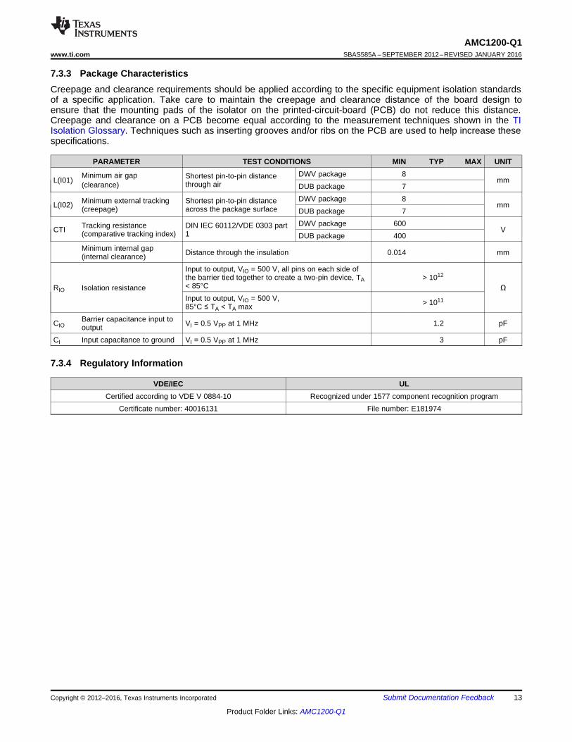
7.3.3 Package CharacteristicsCreepage and clearance requirements should be applied according to the specific equipment isolation standardsof a specific application. Take care to maintain the creepage and clearance distance of the board design toensure that the mounting pads of the isolator on the printed-circuit-board (PCB) do not reduce this distance.Creepage and clearance on a PCB become equal according to the measurement techniques shown in the TIIsolation Glossary. Techniques such as inserting grooves and/or ribs on the PCB are used to help increase thesespecifications.
PARAMETER TEST CONDITIONS MIN TYP MAX UNIT
L(I01) Minimum air gap(clearance)
Shortest pin-to-pin distancethrough air
DWV package 8mm
DUB package 7
L(I02) Minimum external tracking(creepage)
Shortest pin-to-pin distanceacross the package surface
DWV package 8mm
DUB package 7
CTI Tracking resistance(comparative tracking index)
DIN IEC 60112/VDE 0303 part1
DWV package 600V
DUB package 400Minimum internal gap(internal clearance) Distance through the insulation 0.014 mm
RIO Isolation resistance
Input to output, VIO = 500 V, all pins on each side ofthe barrier tied together to create a two-pin device, TA< 85°C
> 1012
ΩInput to output, VIO = 500 V,85°C ≤ TA < TA max > 1011
CIOBarrier capacitance input tooutput VI = 0.5 VPP at 1 MHz 1.2 pF
CI Input capacitance to ground VI = 0.5 VPP at 1 MHz 3 pF
7.3.4 Regulatory Information
VDE/IEC ULCertified according to VDE V 0884-10 Recognized under 1577 component recognition program
Certificate number: 40016131 File number: E181974
S1
S1
C = 3 pFINP
C = 3 pFINN
VINN
VINP
VDD1
GND1
GND1
GND1
3 pF
R = 28 kWIN
3 pF
VINN
VINPEquivalent
Circuit
R =IN f x CCLK DIFF
1
( = 10 MHz)fCLK
C = 3.6 pFIND
GND1
GND1
400 W
400 W
S2
S2
GND1 + 0.8 V
GND1 + 0.8 V
14
AMC1200-Q1SBAS585A –SEPTEMBER 2012–REVISED JANUARY 2016 www.ti.com
Product Folder Links: AMC1200-Q1
Submit Documentation Feedback Copyright © 2012–2016, Texas Instruments Incorporated
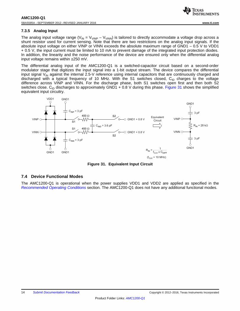
7.3.5 Analog InputThe analog input voltage range (VIN = VVINP – VVINN) is tailored to directly accommodate a voltage drop across ashunt resistor used for current sensing. Note that there are two restrictions on the analog input signals. If theabsolute input voltage on either VINP or VINN exceeds the absolute maximum range of GND1 – 0.5 V to VDD1+ 0.5 V, the input current must be limited to 10 mA to prevent damage of the integrated input protection diodes.In addition, the linearity and the noise performance of the device are ensured only when the differential analoginput voltage remains within ±250 mV.
The differential analog input of the AMC1200-Q1 is a switched-capacitor circuit based on a second-ordermodulator stage that digitizes the input signal into a 1-bit output stream. The device compares the differentialinput signal VIN against the internal 2.5-V reference using internal capacitors that are continuously charged anddischarged with a typical frequency of 10 MHz. With the S1 switches closed, CID charges to the voltagedifference across VINP and VINN. For the discharge phase, both S1 switches open first and then both S2switches close. CID discharges to approximately GND1 + 0.8 V during this phase. Figure 31 shows the simplifiedequivalent input circuitry.
Figure 31. Equivalent Input Circuit
7.4 Device Functional ModesThe AMC1200-Q1 is operational when the power supplies VDD1 and VDD2 are applied as specified in theRecommended Operating Conditions section. The AMC1200-Q1 does not have any additional functional modes.
R2
12 W
R3
12 WRSHUNT
AMC1200-Q1
Gated
Drive
Circuit
To Load
FloatingPower SupplyHV+
Isolation
Barrier
C2(1)
330 pF
C3
10 pF
(Optional)
VDD1
VINP
VINN
GND1
VDD2
VOUTP
VOUTN
GND2
C4
10 pF
(Optional)
C1(1)
0.1 Fm
D1
5.1 V
R1
Gated
Drive
Circuit
PowerSupply
HV-
C5(1)
0.1 Fm
ADC
TMC320
C/F28xxx
15
AMC1200-Q1www.ti.com SBAS585A –SEPTEMBER 2012–REVISED JANUARY 2016
Product Folder Links: AMC1200-Q1
Submit Documentation FeedbackCopyright © 2012–2016, Texas Instruments Incorporated
8 Application and Implementation
NOTEInformation in the following applications sections is not part of the TI componentspecification, and TI does not warrant its accuracy or completeness. TI’s customers areresponsible for determining suitability of components for their purposes. Customers shouldvalidate and test their design implementation to confirm system functionality.
8.1 Application InformationThe AMC1200-Q1 offers unique linearity, high input common-mode rejection, low dc errors, and low temperaturedrift. These features make the AMC1200-Q1 a robust, high-performance isolation amplifier for automotiveapplications where high voltage isolation is required.
8.2 Typical Applications
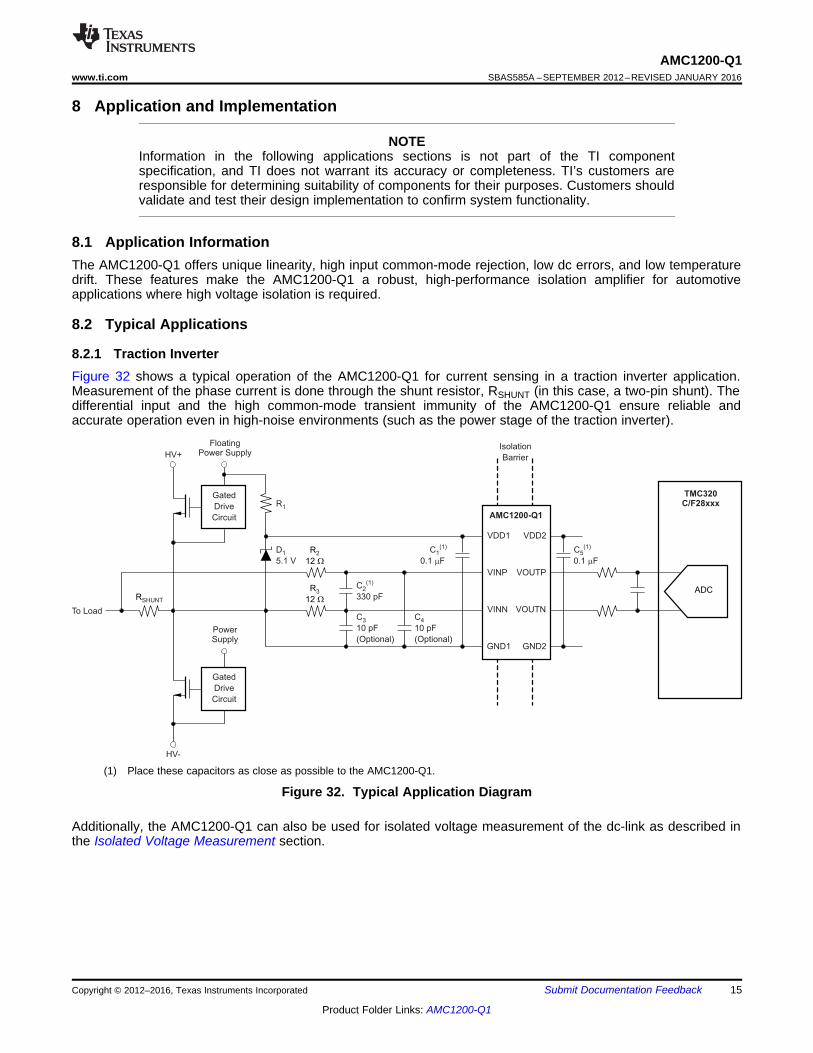
8.2.1 Traction InverterFigure 32 shows a typical operation of the AMC1200-Q1 for current sensing in a traction inverter application.Measurement of the phase current is done through the shunt resistor, RSHUNT (in this case, a two-pin shunt). Thedifferential input and the high common-mode transient immunity of the AMC1200-Q1 ensure reliable andaccurate operation even in high-noise environments (such as the power stage of the traction inverter).
(1) Place these capacitors as close as possible to the AMC1200-Q1.
Figure 32. Typical Application Diagram
Additionally, the AMC1200-Q1 can also be used for isolated voltage measurement of the dc-link as described inthe Isolated Voltage Measurement section.
16
AMC1200-Q1SBAS585A –SEPTEMBER 2012–REVISED JANUARY 2016 www.ti.com
Product Folder Links: AMC1200-Q1
Submit Documentation Feedback Copyright © 2012–2016, Texas Instruments Incorporated
Typical Applications (continued)8.2.1.1 Design RequirementsTable 3 lists the parameters for the typical application in Figure 32.
Table 3. Design RequirementsPARAMETER VALUE
High-side supply voltage 5 VLow-side supply voltage 3 V, or 3.3 V, or 5 V
Voltage drop across shunt for linear response ±250 mV (max)
8.2.1.2 Detailed Design ProcedureThe high-side power supply (VDD1) for the AMC1200-Q1 is derived from the power supply of the upper gatedriver. Further details are provided in the Power Supply Recommendations section.
The floating ground reference (GND1) is derived from one of the ends of the shunt resistor that is connected tothe negative input of the AMC1200-Q1 (VINN). If a four-pin shunt is used, the inputs of the AMC1200-Q1 areconnected to the inner leads and GND1 is connected to one of the outer shunt leads.
Use Ohm's Law to calculate the voltage drop across the shunt resistor (VSHUNT) for the desired current to bemeasured: VSHUNT = I × RSHUNT.
Consider the following two restrictions to choose the proper value of the shunt resistor RSHUNT:• The voltage drop caused by the nominal current range must not exceed the recommended differential input
voltage range: VSHUNT ≤ ±250 mV• The voltage drop caused by the maximum allowed overcurrent must not exceed the input voltage that causes
a clipping output: VSHUNT ≤ VClipping
For best performance, use an RC filter (components R2, R3, and C2 in Figure 32) to limit the noise bandwidth ofthe differential input signal. Limiting the value of resistors R2 and R3 to less than 24 Ω is recommended to avoidincomplete settling of the AMC1200-Q1 input circuitry (see Analog Input).
Optionally, the common-mode capacitors C3 and C4 can be used to reduce charge dumping from the inputs.Mismatch in values of C3 and C4 leads to a common-mode error at the modulator input. In this case, choose thevalue of the differential filter capacitor C2 to be at least 10 times larger than the values of C3 and C4 to limit theeffect of the common-mode error. NP0-type capacitors are recommended to be used for C2, C3 and C4.
The differential output of the AMC1200-Q1 can either directly drive an analog-to-digital converter (ADC) input orcan be further filtered before being processed by an ADC. For more information on the general procedure todesign the filtering and driving stages for SAR ADCs, consult the TI Precision Designs 18 bit, 1Msps DataAcquisition Block Optimized for Lowest Distortion and Noise (SLAU515), and 18 bit Data Acquisition BlockOptimized for Lowest Power (SLAU513) available for download at www.ti.com.
RIN
R2
R1
L1
L2
G = G +ERRTOT ERR
R2
RIN
−0.1
−0.08
−0.06
−0.04
−0.02
0
0.02
0.04
0.06
0.08
0.1
−250 −200 −150 −100 −50 0 50 100 150 200 250Input Voltage (mV)
Non
linea
rity
(%)
VDD2 = 3 VVDD2 = 5 V
Time (2 s/div)m
200 mV/div
500 mV/div
500 mV/div
17
AMC1200-Q1www.ti.com SBAS585A –SEPTEMBER 2012–REVISED JANUARY 2016
Product Folder Links: AMC1200-Q1
Submit Documentation FeedbackCopyright © 2012–2016, Texas Instruments Incorporated
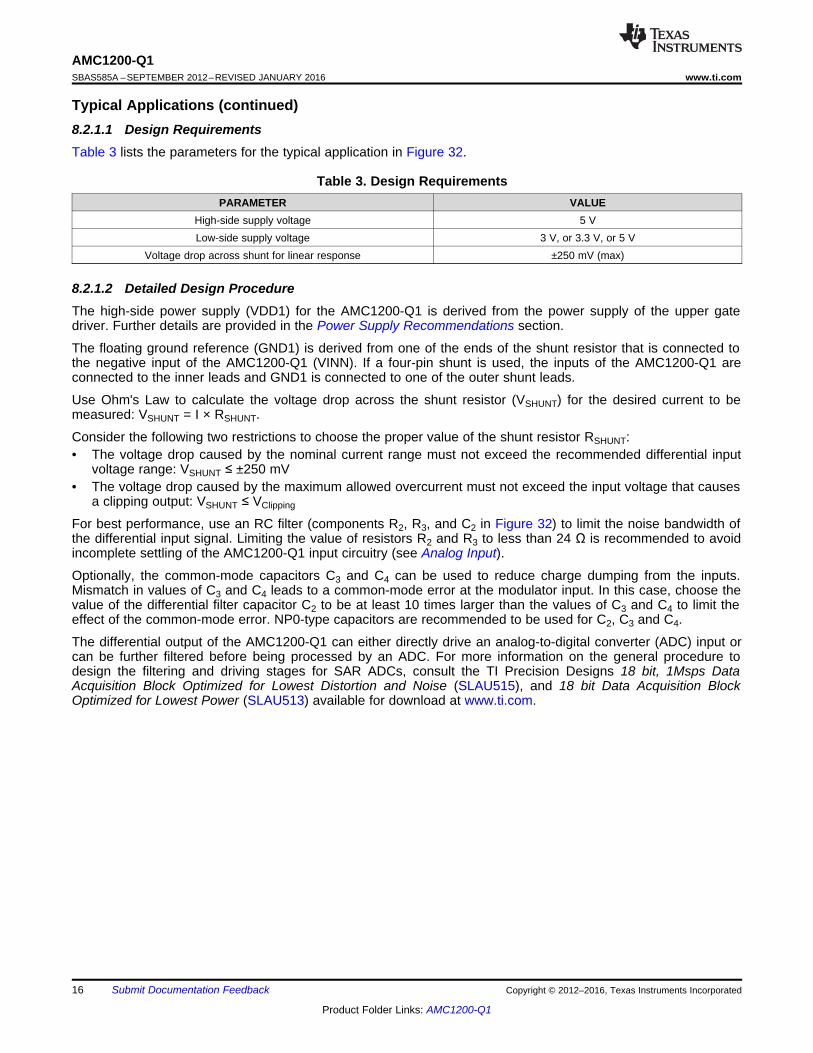
8.2.1.3 Application CurvesIn traction inverter applications, the power switches must be protected in case of an overcurrent condition. Toallow fast powering off of the system, a low delay caused by the isolation amplifier is required. Figure 33 showsthe typical full-scale step response of the AMC1200-Q1.
The high linearity of the AMC1200-Q1, as shown in Figure 34, allows design of traction inverters with low torqueripple.
Figure 33. Step Response of the AMC1200-Q1 Figure 34. Typical Nonlinearity of the AMC1200-Q1
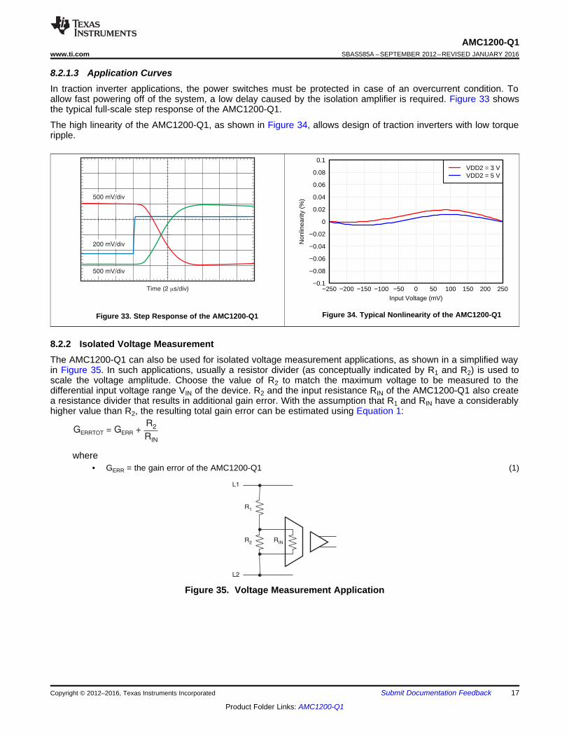
8.2.2 Isolated Voltage MeasurementThe AMC1200-Q1 can also be used for isolated voltage measurement applications, as shown in a simplified wayin Figure 35. In such applications, usually a resistor divider (as conceptually indicated by R1 and R2) is used toscale the voltage amplitude. Choose the value of R2 to match the maximum voltage to be measured to thedifferential input voltage range VIN of the device. R2 and the input resistance RIN of the AMC1200-Q1 also createa resistance divider that results in additional gain error. With the assumption that R1 and RIN have a considerablyhigher value than R2, the resulting total gain error can be estimated using Equation 1:
where• GERR = the gain error of the AMC1200-Q1 (1)
Figure 35. Voltage Measurement Application
VOUTP
VOUTN
VDD2
GND2GND1
VINN
VINP
VDD1
AMC1200-Q1
HV+
HV-
To Load
FloatingPower Supply,
20 V
3.3 V or 5.0 V
RSHUNT
Gate Driver
Gate Driver
5.1 V
R1
800
Z1
1N751A C1
0.1 F
R2
12
R3
12
C3
330 pF
C4
0.1 F
ADS7263
18
AMC1200-Q1SBAS585A –SEPTEMBER 2012–REVISED JANUARY 2016 www.ti.com
Product Folder Links: AMC1200-Q1
Submit Documentation Feedback Copyright © 2012–2016, Texas Instruments Incorporated
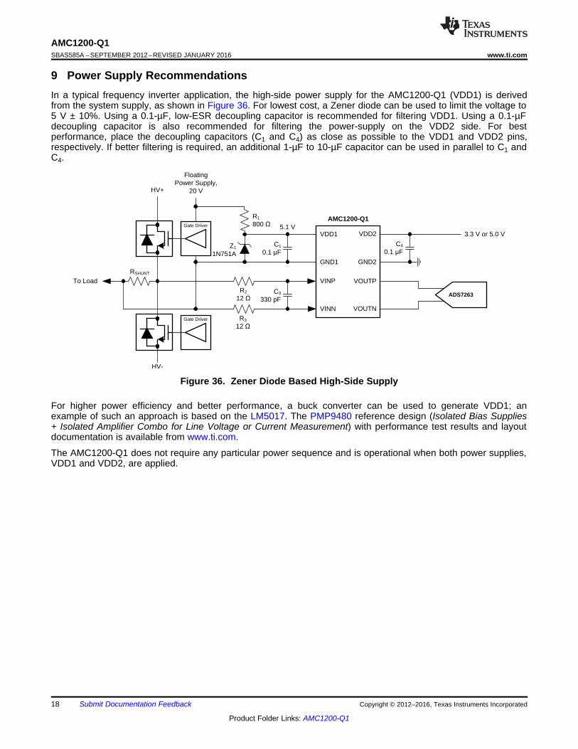
9 Power Supply RecommendationsIn a typical frequency inverter application, the high-side power supply for the AMC1200-Q1 (VDD1) is derivedfrom the system supply, as shown in Figure 36. For lowest cost, a Zener diode can be used to limit the voltage to5 V ± 10%. Using a 0.1-µF, low-ESR decoupling capacitor is recommended for filtering VDD1. Using a 0.1-µFdecoupling capacitor is also recommended for filtering the power-supply on the VDD2 side. For bestperformance, place the decoupling capacitors (C1 and C4) as close as possible to the VDD1 and VDD2 pins,respectively. If better filtering is required, an additional 1-µF to 10-µF capacitor can be used in parallel to C1 andC4.
Figure 36. Zener Diode Based High-Side Supply
For higher power efficiency and better performance, a buck converter can be used to generate VDD1; anexample of such an approach is based on the LM5017. The PMP9480 reference design (Isolated Bias Supplies+ Isolated Amplifier Combo for Line Voltage or Current Measurement) with performance test results and layoutdocumentation is available from www.ti.com.
The AMC1200-Q1 does not require any particular power sequence and is operational when both power supplies,VDD1 and VDD2, are applied.
Top View
Clearance area.Keep free of any
conductive materials.
AMC1200-Q1
LEGEND
Top layer; copper pour and traces
High-side area
Controller-side area
Via
To Shunt To Filter or ADC
VDD1
VINP
GND1
VINN
VDD2
VOUTP
VOUTN
GND2
0.1mF
SMD
1206
0.1 µFSMD1206
0.1 µFSMD1206
330 pFSMD0603
12SMD 0603
W
12SMD 0603
W
AMC1200-Q1www.ti.com SBAS585A –SEPTEMBER 2012–REVISED JANUARY 2016
19
Product Folder Links: AMC1200-Q1
Submit Documentation FeedbackCopyright © 2012–2016, Texas Instruments Incorporated
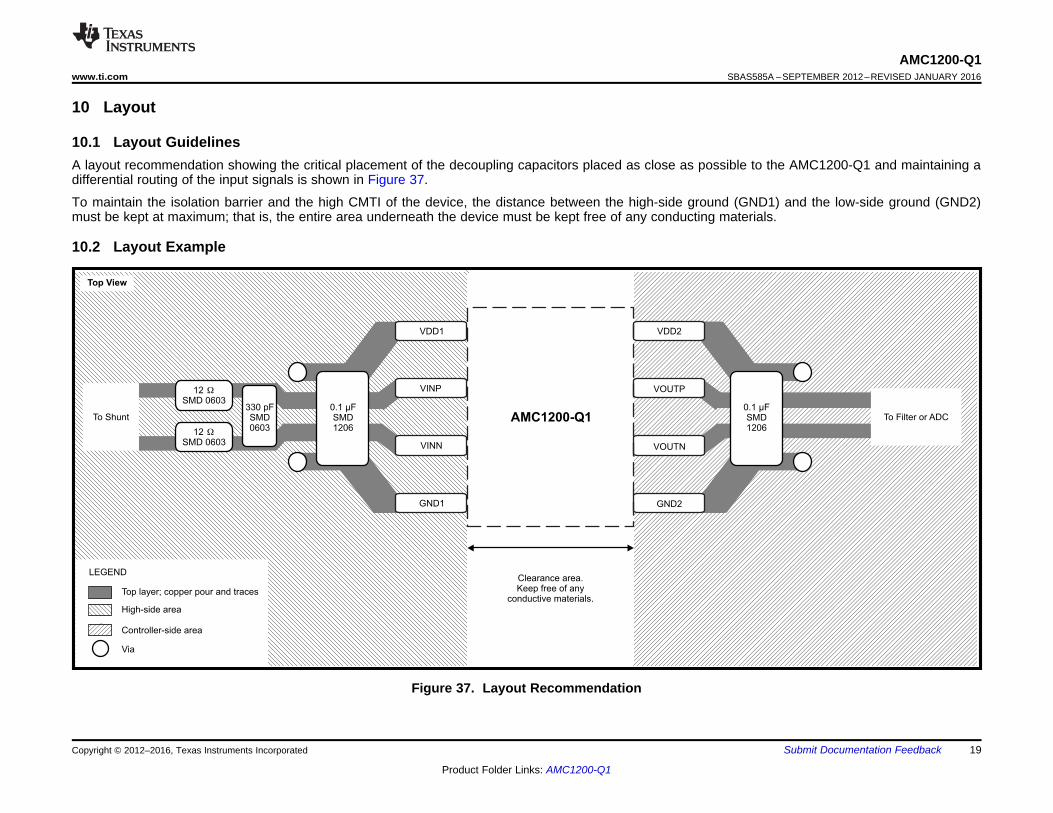
10 Layout
10.1 Layout GuidelinesA layout recommendation showing the critical placement of the decoupling capacitors placed as close as possible to the AMC1200-Q1 and maintaining adifferential routing of the input signals is shown in Figure 37.
To maintain the isolation barrier and the high CMTI of the device, the distance between the high-side ground (GND1) and the low-side ground (GND2)must be kept at maximum; that is, the entire area underneath the device must be kept free of any conducting materials.
10.2 Layout Example
Figure 37. Layout Recommendation
20
AMC1200-Q1SBAS585A –SEPTEMBER 2012–REVISED JANUARY 2016 www.ti.com
Product Folder Links: AMC1200-Q1
Submit Documentation Feedback Copyright © 2012–2016, Texas Instruments Incorporated
11 Device and Documentation Support
11.1 Documentation Support
11.1.1 Related DocumentationFor related documentation see the following:• LM5017 Data Sheet, SNVS783• ADS7263 Data Sheet, SBAS523• TI Isolation Glossary, SLLA353• 18 bit, 1Msps Data Acquisition Block Optimized for Lowest Distortion and Noise, SLAU515• 18 bit Data Acquisition Block Optimized for Lowest Power, SLAU513• High-Voltage Lifetime of the ISO72x Family of Digital Isolators, SLLA197• ISO72x Digital Isolator Magnetic-Field Immunity, SLLA181• AMC1100: Replacement of Input Main Sensing Transformer in Inverters with Isolate Amplifier, SLAA552• Isolated Current Sensing Reference Design Solution, 5A, 2kV, TIPD121• Isolated Bias Supplies + Isolated Amplifier Combo for Line Voltage or Current Measurement, PMP9480• LM5017 Data Sheet, SNVS783
11.2 Community ResourcesThe following links connect to TI community resources. Linked contents are provided "AS IS" by the respectivecontributors. They do not constitute TI specifications and do not necessarily reflect TI's views; see TI's Terms ofUse.
TI E2E™ Online Community TI's Engineer-to-Engineer (E2E) Community. Created to foster collaborationamong engineers. At e2e.ti.com, you can ask questions, share knowledge, explore ideas and helpsolve problems with fellow engineers.
Design Support TI's Design Support Quickly find helpful E2E forums along with design support tools andcontact information for technical support.
11.3 TrademarksE2E is a trademark of Texas Instruments.All other trademarks are the property of their respective owners.
11.4 Electrostatic Discharge CautionThis integrated circuit can be damaged by ESD. Texas Instruments recommends that all integrated circuits be handled withappropriate precautions. Failure to observe proper handling and installation procedures can cause damage.
ESD damage can range from subtle performance degradation to complete device failure. Precision integrated circuits may be moresusceptible to damage because very small parametric changes could cause the device not to meet its published specifications.
11.5 GlossarySLYZ022 — TI Glossary.
This glossary lists and explains terms, acronyms, and definitions.
12 Mechanical, Packaging, and Orderable InformationThe following pages include mechanical, packaging, and orderable information. This information is the mostcurrent data available for the designated devices. This data is subject to change without notice and revision ofthis document. For browser-based versions of this data sheet, refer to the left-hand navigation.
PACKAGE OPTION ADDENDUM
www.ti.com 2-Mar-2016
Addendum-Page 1
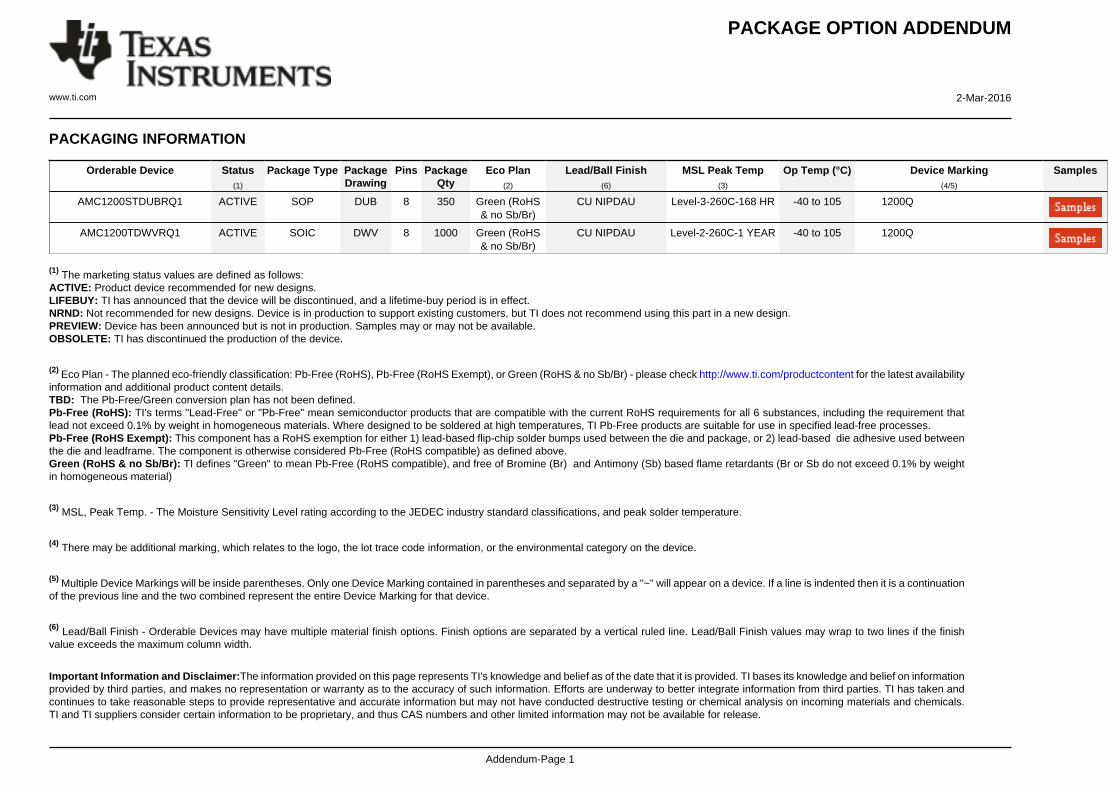
PACKAGING INFORMATION
Orderable Device Status(1)
Package Type PackageDrawing
Pins PackageQty
Eco Plan(2)
Lead/Ball Finish(6)
MSL Peak Temp(3)
Op Temp (°C) Device Marking(4/5)
Samples
AMC1200STDUBRQ1 ACTIVE SOP DUB 8 350 Green (RoHS& no Sb/Br)
CU NIPDAU Level-3-260C-168 HR -40 to 105 1200Q
AMC1200TDWVRQ1 ACTIVE SOIC DWV 8 1000 Green (RoHS& no Sb/Br)
CU NIPDAU Level-2-260C-1 YEAR -40 to 105 1200Q
(1) The marketing status values are defined as follows:ACTIVE: Product device recommended for new designs.LIFEBUY: TI has announced that the device will be discontinued, and a lifetime-buy period is in effect.NRND: Not recommended for new designs. Device is in production to support existing customers, but TI does not recommend using this part in a new design.PREVIEW: Device has been announced but is not in production. Samples may or may not be available.OBSOLETE: TI has discontinued the production of the device.
(2) Eco Plan - The planned eco-friendly classification: Pb-Free (RoHS), Pb-Free (RoHS Exempt), or Green (RoHS & no Sb/Br) - please check http://www.ti.com/productcontent for the latest availabilityinformation and additional product content details.TBD: The Pb-Free/Green conversion plan has not been defined.Pb-Free (RoHS): TI's terms "Lead-Free" or "Pb-Free" mean semiconductor products that are compatible with the current RoHS requirements for all 6 substances, including the requirement thatlead not exceed 0.1% by weight in homogeneous materials. Where designed to be soldered at high temperatures, TI Pb-Free products are suitable for use in specified lead-free processes.Pb-Free (RoHS Exempt): This component has a RoHS exemption for either 1) lead-based flip-chip solder bumps used between the die and package, or 2) lead-based die adhesive used betweenthe die and leadframe. The component is otherwise considered Pb-Free (RoHS compatible) as defined above.Green (RoHS & no Sb/Br): TI defines "Green" to mean Pb-Free (RoHS compatible), and free of Bromine (Br) and Antimony (Sb) based flame retardants (Br or Sb do not exceed 0.1% by weightin homogeneous material)
(3) MSL, Peak Temp. - The Moisture Sensitivity Level rating according to the JEDEC industry standard classifications, and peak solder temperature.
(4) There may be additional marking, which relates to the logo, the lot trace code information, or the environmental category on the device.
(5) Multiple Device Markings will be inside parentheses. Only one Device Marking contained in parentheses and separated by a "~" will appear on a device. If a line is indented then it is a continuationof the previous line and the two combined represent the entire Device Marking for that device.
(6) Lead/Ball Finish - Orderable Devices may have multiple material finish options. Finish options are separated by a vertical ruled line. Lead/Ball Finish values may wrap to two lines if the finishvalue exceeds the maximum column width.
Important Information and Disclaimer:The information provided on this page represents TI's knowledge and belief as of the date that it is provided. TI bases its knowledge and belief on informationprovided by third parties, and makes no representation or warranty as to the accuracy of such information. Efforts are underway to better integrate information from third parties. TI has taken andcontinues to take reasonable steps to provide representative and accurate information but may not have conducted destructive testing or chemical analysis on incoming materials and chemicals.TI and TI suppliers consider certain information to be proprietary, and thus CAS numbers and other limited information may not be available for release.
PACKAGE OPTION ADDENDUM
www.ti.com 2-Mar-2016
Addendum-Page 2
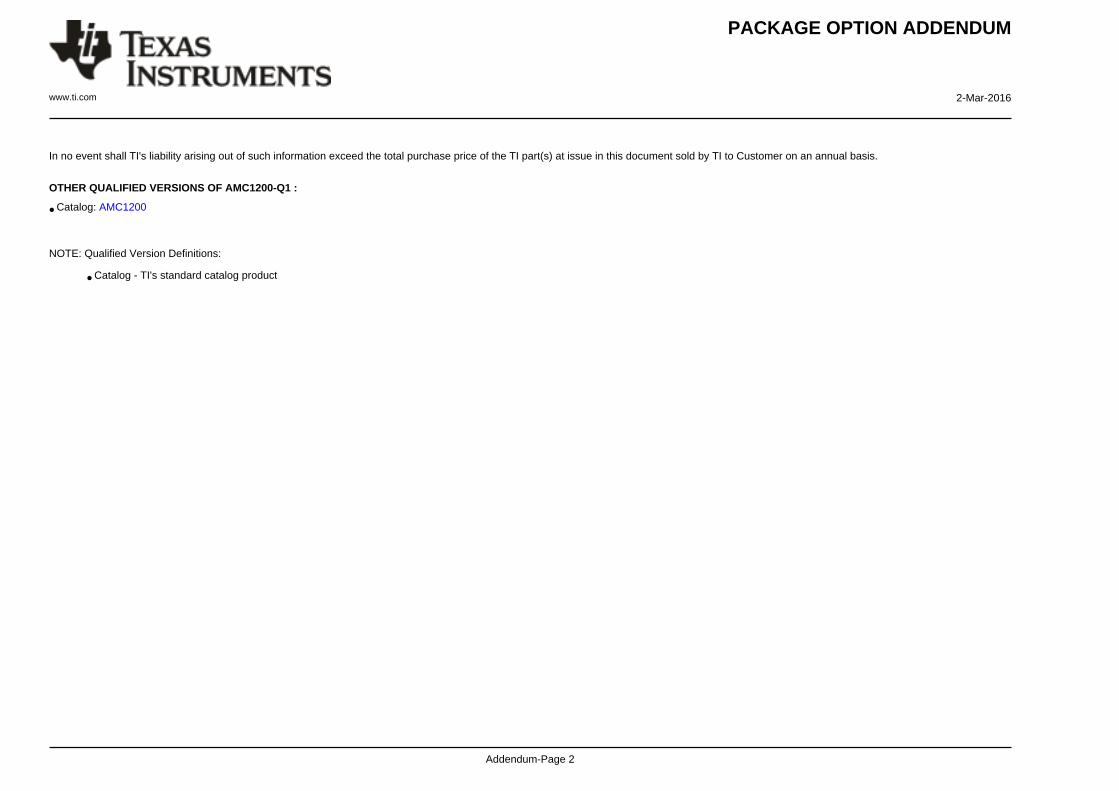
In no event shall TI's liability arising out of such information exceed the total purchase price of the TI part(s) at issue in this document sold by TI to Customer on an annual basis.
OTHER QUALIFIED VERSIONS OF AMC1200-Q1 :
• Catalog: AMC1200
NOTE: Qualified Version Definitions:
• Catalog - TI's standard catalog product
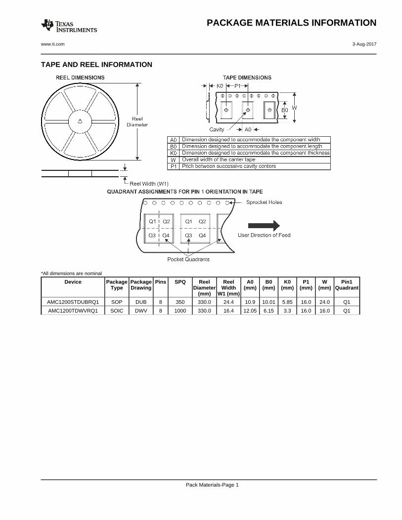
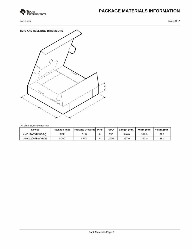
TAPE AND REEL INFORMATION
*All dimensions are nominal
Device PackageType
PackageDrawing
Pins SPQ ReelDiameter
(mm)
ReelWidth
W1 (mm)
A0(mm)
B0(mm)
K0(mm)
P1(mm)
W(mm)
Pin1Quadrant
AMC1200STDUBRQ1 SOP DUB 8 350 330.0 24.4 10.9 10.01 5.85 16.0 24.0 Q1
AMC1200TDWVRQ1 SOIC DWV 8 1000 330.0 16.4 12.05 6.15 3.3 16.0 16.0 Q1
PACKAGE MATERIALS INFORMATION
www.ti.com 3-Aug-2017
Pack Materials-Page 1
*All dimensions are nominal
Device Package Type Package Drawing Pins SPQ Length (mm) Width (mm) Height (mm)
AMC1200STDUBRQ1 SOP DUB 8 350 346.0 346.0 29.0
AMC1200TDWVRQ1 SOIC DWV 8 1000 367.0 367.0 38.0
PACKAGE MATERIALS INFORMATION
www.ti.com 3-Aug-2017
Pack Materials-Page 2
www.ti.com
PACKAGE OUTLINE
C10.710.1 TYP
6X 2.54
4X(1.524)
2X7.62
0.3550.204 TYP
0 - 4
8X 0.5550.355
6.626.52
0.38 MIN
0.635GAGE PLANE
4.85 MAX
1.451.15
A
9.559.02
NOTE 3
B 6.676.57
4X (0.99)
4222355/D 08/2017
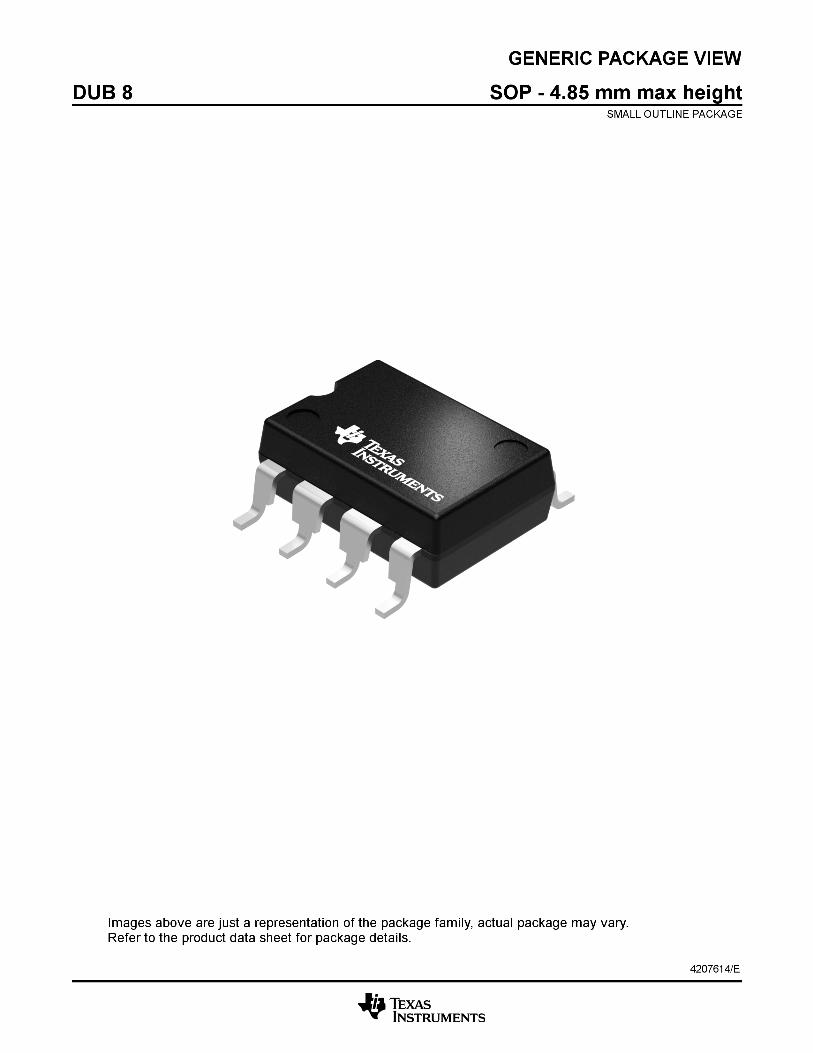
SOP - 4.85 mm max heightDUB0008ASMALL OUTLINE PACKAGE
NOTES: 1. All linear dimensions are in millimeters. Any dimensions in parenthesis are for reference only. Dimensioning and tolerancing per ASME Y14.5M. 2. This drawing is subject to change without notice. 3. This dimension does not include mold flash, protrusions, or gate burrs. Mold flash, protrusions, or gate burrs shall not exceed 0.254 mm per side.
18
0.1 C A B
54
PIN 1 ID
ALTERNATEPIN 1 ID
SEATING PLANE
0.1 C
SEE DETAIL A
TOP MOLD
DETAIL ATYPICAL
SCALE 1.200
www.ti.com
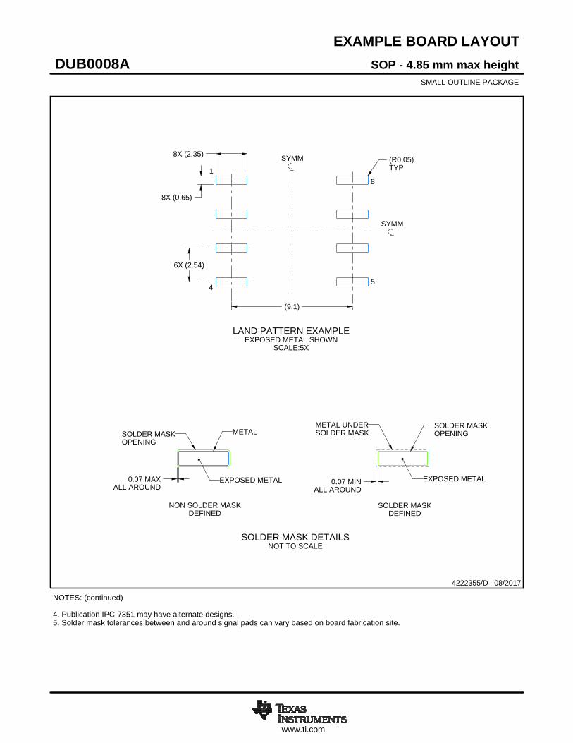
EXAMPLE BOARD LAYOUT
(9.1)
0.07 MAXALL AROUND
0.07 MINALL AROUND
8X (2.35)
8X (0.65)
6X (2.54)
(R0.05)TYP
4222355/D 08/2017
SOP - 4.85 mm max heightDUB0008ASMALL OUTLINE PACKAGE
SYMM
SYMM
LAND PATTERN EXAMPLEEXPOSED METAL SHOWN
SCALE:5X
1
45
8
NOTES: (continued) 4. Publication IPC-7351 may have alternate designs. 5. Solder mask tolerances between and around signal pads can vary based on board fabrication site.
METALSOLDER MASKOPENING
NON SOLDER MASKDEFINED
SOLDER MASK DETAILSNOT TO SCALE
EXPOSED METAL
SOLDER MASKOPENING
METAL UNDERSOLDER MASK
SOLDER MASKDEFINED
EXPOSED METAL
www.ti.com
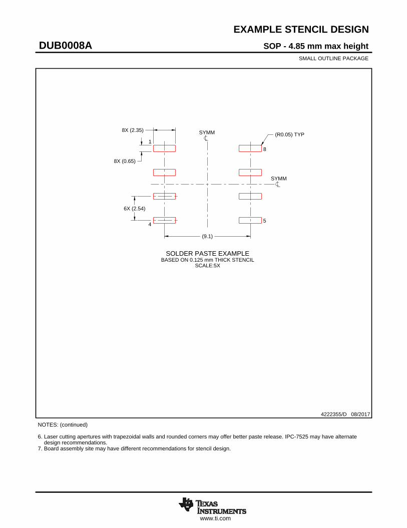
EXAMPLE STENCIL DESIGN
(9.1)
6X (2.54)
8X (0.65)
8X (2.35)(R0.05) TYP
4222355/D 08/2017
SOP - 4.85 mm max heightDUB0008ASMALL OUTLINE PACKAGE
NOTES: (continued) 6. Laser cutting apertures with trapezoidal walls and rounded corners may offer better paste release. IPC-7525 may have alternate design recommendations. 7. Board assembly site may have different recommendations for stencil design.
SYMM
SYMM
1
45
8
SOLDER PASTE EXAMPLEBASED ON 0.125 mm THICK STENCIL
SCALE:5X
www.ti.com
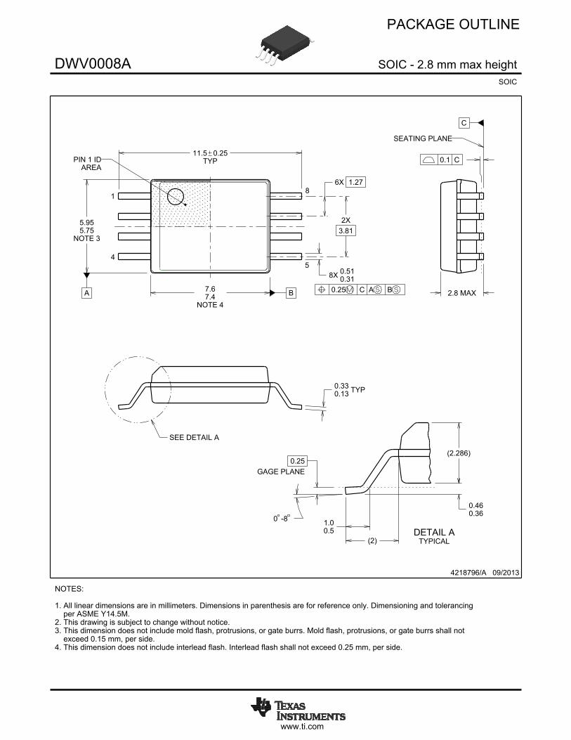
PACKAGE OUTLINE
C
TYP11.5 0.25
2.8 MAX
TYP0.330.13
0 -8
6X 1.27
8X 0.510.31
2X3.81
0.460.36
1.00.5
0.25GAGE PLANE
A
NOTE 3
5.955.75
BNOTE 4
7.67.4
(2.286)
(2)
4218796/A 09/2013
SOIC - 2.8 mm max heightDWV0008ASOIC
NOTES: 1. All linear dimensions are in millimeters. Dimensions in parenthesis are for reference only. Dimensioning and tolerancing per ASME Y14.5M. 2. This drawing is subject to change without notice. 3. This dimension does not include mold flash, protrusions, or gate burrs. Mold flash, protrusions, or gate burrs shall not exceed 0.15 mm, per side. 4. This dimension does not include interlead flash. Interlead flash shall not exceed 0.25 mm, per side.
18
0.25 C A B
54
AREAPIN 1 ID
SEATING PLANE
0.1 C
SEE DETAIL A
DETAIL ATYPICAL
SCALE 2.000
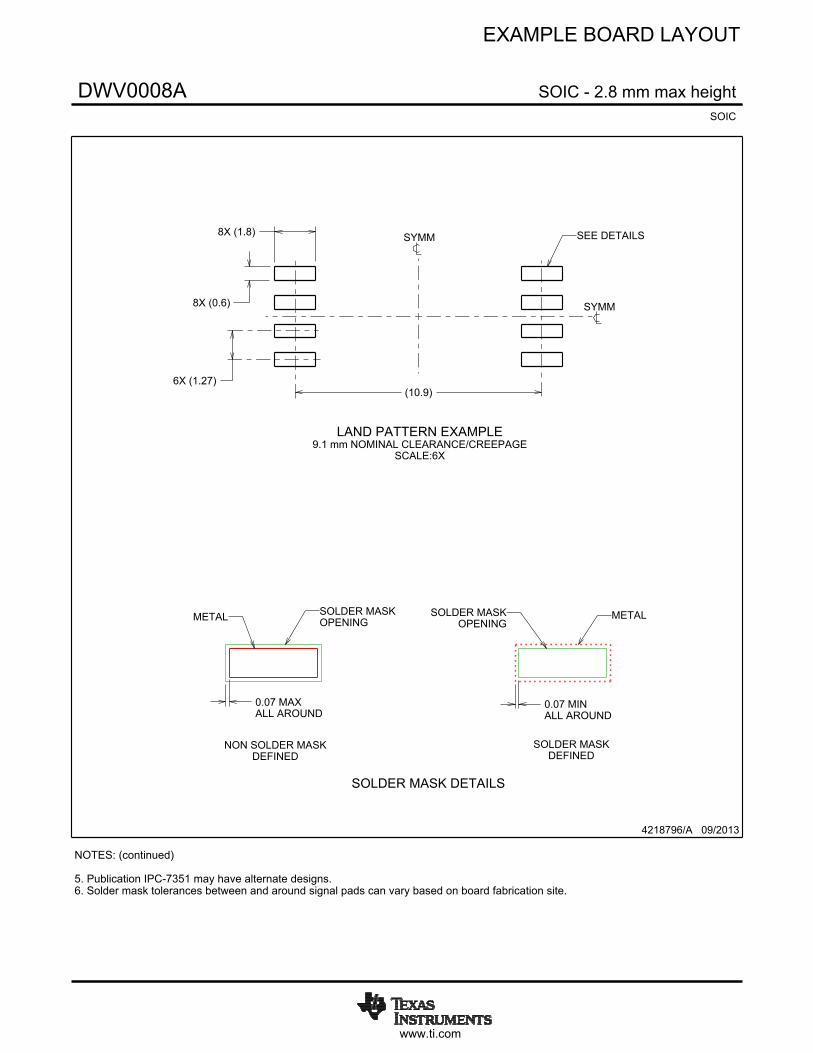
www.ti.com
EXAMPLE BOARD LAYOUT
(10.9)
0.07 MAXALL AROUND
0.07 MINALL AROUND
8X (1.8)
8X (0.6)
6X (1.27)
4218796/A 09/2013
SOIC - 2.8 mm max heightDWV0008ASOIC
SYMM
SYMM
SEE DETAILS
LAND PATTERN EXAMPLE9.1 mm NOMINAL CLEARANCE/CREEPAGE
SCALE:6X
NOTES: (continued) 5. Publication IPC-7351 may have alternate designs. 6. Solder mask tolerances between and around signal pads can vary based on board fabrication site.
METAL SOLDER MASKOPENING
NON SOLDER MASKDEFINED
SOLDER MASK DETAILS
OPENINGSOLDER MASK METAL
SOLDER MASKDEFINED
www.ti.com
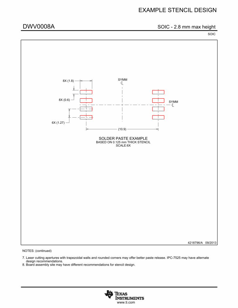
EXAMPLE STENCIL DESIGN
8X (1.8)
8X (0.6)
6X (1.27)
(10.9)
4218796/A 09/2013
SOIC - 2.8 mm max heightDWV0008ASOIC
NOTES: (continued) 7. Laser cutting apertures with trapezoidal walls and rounded corners may offer better paste release. IPC-7525 may have alternate design recommendations. 8. Board assembly site may have different recommendations for stencil design.
SOLDER PASTE EXAMPLEBASED ON 0.125 mm THICK STENCIL
SCALE:6X
SYMM
SYMM
IMPORTANT NOTICE
Texas Instruments Incorporated (TI) reserves the right to make corrections, enhancements, improvements and other changes to itssemiconductor products and services per JESD46, latest issue, and to discontinue any product or service per JESD48, latest issue. Buyersshould obtain the latest relevant information before placing orders and should verify that such information is current and complete.TI’s published terms of sale for semiconductor products (http://www.ti.com/sc/docs/stdterms.htm) apply to the sale of packaged integratedcircuit products that TI has qualified and released to market. Additional terms may apply to the use or sale of other types of TI products andservices.Reproduction of significant portions of TI information in TI data sheets is permissible only if reproduction is without alteration and isaccompanied by all associated warranties, conditions, limitations, and notices. TI is not responsible or liable for such reproduceddocumentation. Information of third parties may be subject to additional restrictions. Resale of TI products or services with statementsdifferent from or beyond the parameters stated by TI for that product or service voids all express and any implied warranties for theassociated TI product or service and is an unfair and deceptive business practice. TI is not responsible or liable for any such statements.Buyers and others who are developing systems that incorporate TI products (collectively, “Designers”) understand and agree that Designersremain responsible for using their independent analysis, evaluation and judgment in designing their applications and that Designers havefull and exclusive responsibility to assure the safety of Designers' applications and compliance of their applications (and of all TI productsused in or for Designers’ applications) with all applicable regulations, laws and other applicable requirements. Designer represents that, withrespect to their applications, Designer has all the necessary expertise to create and implement safeguards that (1) anticipate dangerousconsequences of failures, (2) monitor failures and their consequences, and (3) lessen the likelihood of failures that might cause harm andtake appropriate actions. Designer agrees that prior to using or distributing any applications that include TI products, Designer willthoroughly test such applications and the functionality of such TI products as used in such applications.TI’s provision of technical, application or other design advice, quality characterization, reliability data or other services or information,including, but not limited to, reference designs and materials relating to evaluation modules, (collectively, “TI Resources”) are intended toassist designers who are developing applications that incorporate TI products; by downloading, accessing or using TI Resources in anyway, Designer (individually or, if Designer is acting on behalf of a company, Designer’s company) agrees to use any particular TI Resourcesolely for this purpose and subject to the terms of this Notice.TI’s provision of TI Resources does not expand or otherwise alter TI’s applicable published warranties or warranty disclaimers for TIproducts, and no additional obligations or liabilities arise from TI providing such TI Resources. TI reserves the right to make corrections,enhancements, improvements and other changes to its TI Resources. TI has not conducted any testing other than that specificallydescribed in the published documentation for a particular TI Resource.Designer is authorized to use, copy and modify any individual TI Resource only in connection with the development of applications thatinclude the TI product(s) identified in such TI Resource. NO OTHER LICENSE, EXPRESS OR IMPLIED, BY ESTOPPEL OR OTHERWISETO ANY OTHER TI INTELLECTUAL PROPERTY RIGHT, AND NO LICENSE TO ANY TECHNOLOGY OR INTELLECTUAL PROPERTYRIGHT OF TI OR ANY THIRD PARTY IS GRANTED HEREIN, including but not limited to any patent right, copyright, mask work right, orother intellectual property right relating to any combination, machine, or process in which TI products or services are used. Informationregarding or referencing third-party products or services does not constitute a license to use such products or services, or a warranty orendorsement thereof. Use of TI Resources may require a license from a third party under the patents or other intellectual property of thethird party, or a license from TI under the patents or other intellectual property of TI.TI RESOURCES ARE PROVIDED “AS IS” AND WITH ALL FAULTS. TI DISCLAIMS ALL OTHER WARRANTIES ORREPRESENTATIONS, EXPRESS OR IMPLIED, REGARDING RESOURCES OR USE THEREOF, INCLUDING BUT NOT LIMITED TOACCURACY OR COMPLETENESS, TITLE, ANY EPIDEMIC FAILURE WARRANTY AND ANY IMPLIED WARRANTIES OFMERCHANTABILITY, FITNESS FOR A PARTICULAR PURPOSE, AND NON-INFRINGEMENT OF ANY THIRD PARTY INTELLECTUALPROPERTY RIGHTS. TI SHALL NOT BE LIABLE FOR AND SHALL NOT DEFEND OR INDEMNIFY DESIGNER AGAINST ANY CLAIM,INCLUDING BUT NOT LIMITED TO ANY INFRINGEMENT CLAIM THAT RELATES TO OR IS BASED ON ANY COMBINATION OFPRODUCTS EVEN IF DESCRIBED IN TI RESOURCES OR OTHERWISE. IN NO EVENT SHALL TI BE LIABLE FOR ANY ACTUAL,DIRECT, SPECIAL, COLLATERAL, INDIRECT, PUNITIVE, INCIDENTAL, CONSEQUENTIAL OR EXEMPLARY DAMAGES INCONNECTION WITH OR ARISING OUT OF TI RESOURCES OR USE THEREOF, AND REGARDLESS OF WHETHER TI HAS BEENADVISED OF THE POSSIBILITY OF SUCH DAMAGES.Unless TI has explicitly designated an individual product as meeting the requirements of a particular industry standard (e.g., ISO/TS 16949and ISO 26262), TI is not responsible for any failure to meet such industry standard requirements.Where TI specifically promotes products as facilitating functional safety or as compliant with industry functional safety standards, suchproducts are intended to help enable customers to design and create their own applications that meet applicable functional safety standardsand requirements. Using products in an application does not by itself establish any safety features in the application. Designers mustensure compliance with safety-related requirements and standards applicable to their applications. Designer may not use any TI products inlife-critical medical equipment unless authorized officers of the parties have executed a special contract specifically governing such use.Life-critical medical equipment is medical equipment where failure of such equipment would cause serious bodily injury or death (e.g., lifesupport, pacemakers, defibrillators, heart pumps, neurostimulators, and implantables). Such equipment includes, without limitation, allmedical devices identified by the U.S. Food and Drug Administration as Class III devices and equivalent classifications outside the U.S.TI may expressly designate certain products as completing a particular qualification (e.g., Q100, Military Grade, or Enhanced Product).Designers agree that it has the necessary expertise to select the product with the appropriate qualification designation for their applicationsand that proper product selection is at Designers’ own risk. Designers are solely responsible for compliance with all legal and regulatoryrequirements in connection with such selection.Designer will fully indemnify TI and its representatives against any damages, costs, losses, and/or liabilities arising out of Designer’s non-compliance with the terms and provisions of this Notice.
Mailing Address: Texas Instruments, Post Office Box 655303, Dallas, Texas 75265Copyright © 2017, Texas Instruments Incorporated