Embed Size (px)
Citation preview
YA
Copyright © 2016, Texas Instruments Incorporated
Product
Folder
Sample &Buy
Technical
Documents
Tools &
Software
Support &Community
An IMPORTANT NOTICE at the end of this data sheet addresses availability, warranty, changes, use in safety-critical applications,intellectual property matters and other important disclaimers. PRODUCTION DATA.
SN54HCT14, SN74HCT14SCLS225G –JULY 1995–REVISED NOVEMBER 2016
SNx4HCT14 Hex Schmitt-Trigger Inverters
1
1 Features1• Operating Voltage Range of 4.5 V to 5.5 V• Outputs Can Drive Up to 10 LSTTL Loads• Low Power Consumption: 20-µA Maximum ICC
• Typical tpd = 18 ns• ±4-mA Output Drive at 5 V• Maximum Low Input Current of 1 µA Maximum• Inputs Are TTL-Voltage Compatible
2 Applications• UPS• White Goods• Computer Peripherals• Printers• AC Servo Drives• Desktop Computers
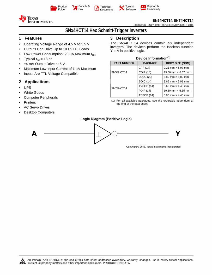
3 DescriptionThe SNx4HCT14 devices contain six independentinverters. The devices perform the Boolean functionY = A in positive logic.
Device Information(1)
PART NUMBER PACKAGE BODY SIZE (NOM)
SN54HCT14CFP (14) 9.21 mm × 5.97 mmCDIP (14) 19.56 mm × 6.67 mmLCCC (20) 8.89 mm × 8.89 mm
SN74HCT14
SOIC (14) 8.65 mm × 3.91 mmTVSOP (14) 3.60 mm × 4.40 mmPDIP (14) 19.30 mm × 6.35 mmTSSOP (14) 5.00 mm × 4.40 mm
(1) For all available packages, see the orderable addendum atthe end of the data sheet.
Logic Diagram (Positive Logic)
2
SN54HCT14, SN74HCT14SCLS225G –JULY 1995–REVISED NOVEMBER 2016 www.ti.com
Product Folder Links: SN54HCT14 SN74HCT14
Submit Documentation Feedback Copyright © 1995–2016, Texas Instruments Incorporated
Table of Contents1 Features .................................................................. 12 Applications ........................................................... 13 Description ............................................................. 14 Revision History..................................................... 25 Pin Configuration and Functions ......................... 36 Specifications......................................................... 4
6.1 Absolute Maximum Ratings ...................................... 46.2 ESD Ratings.............................................................. 46.3 Recommended Operating Conditions....................... 46.4 Thermal Information .................................................. 46.5 Electrical Characteristics........................................... 56.6 Switching Characteristics .......................................... 66.7 Operating Characteristics.......................................... 66.8 Typical Characteristics .............................................. 6
7 Parameter Measurement Information .................. 78 Detailed Description .............................................. 8
8.1 Overview ................................................................... 88.2 Functional Block Diagram ......................................... 8
8.3 Feature Description................................................... 88.4 Device Functional Modes.......................................... 8
9 Application and Implementation .......................... 99.1 Application Information.............................................. 99.2 Typical Application .................................................... 9
10 Power Supply Recommendations ..................... 1011 Layout................................................................... 10
11.1 Layout Guidelines ................................................. 1011.2 Layout Example .................................................... 10
12 Device and Documentation Support ................. 1112.1 Documentation Support ........................................ 1112.2 Related Links ........................................................ 1112.3 Receiving Notification of Documentation Updates 1112.4 Community Resource............................................ 1112.5 Trademarks ........................................................... 1112.6 Electrostatic Discharge Caution............................ 1112.7 Glossary ................................................................ 11
13 Mechanical, Packaging, and OrderableInformation ........................................................... 11
4 Revision HistoryNOTE: Page numbers for previous revisions may differ from page numbers in the current version.
Changes from Revision F (October 2010) to Revision G Page
• Added ESD Ratings table, Feature Description section, Device Functional Modes, Application and Implementationsection, Power Supply Recommendations section, Layout section, Device and Documentation Support section, andMechanical, Packaging, and Orderable Information section ................................................................................................. 1
• Deleted Ordering Information table; see Package Option Addendum at the end of the data sheet ...................................... 1• Changed Package thermal impedance, RθJA, values in Thermal Information table From: 86 To: 90.9 (D), From: 96
To: 105 (DB), From: 127 To: 132.2 (DGV), From: 80 To: 55.3 (N), and From: 113 To: 120.2 (PW)..................................... 4
42A
5NC
62Y
7NC
83A
93Y
10G
ND
11N
C
124Y
134A
14 5Y
15 NC
16 5A
17 NC
18 6Y
196A
20V
CC
1N
C
21A
31Y
Not to scale
11A 14 VCC
21Y 13 6A
32A 12 6Y
42Y 11 5A
53A 10 5Y
63Y 9 4A
7GND 8 4Y
Not to scale
3
SN54HCT14, SN74HCT14www.ti.com SCLS225G –JULY 1995–REVISED NOVEMBER 2016
Product Folder Links: SN54HCT14 SN74HCT14
Submit Documentation FeedbackCopyright © 1995–2016, Texas Instruments Incorporated
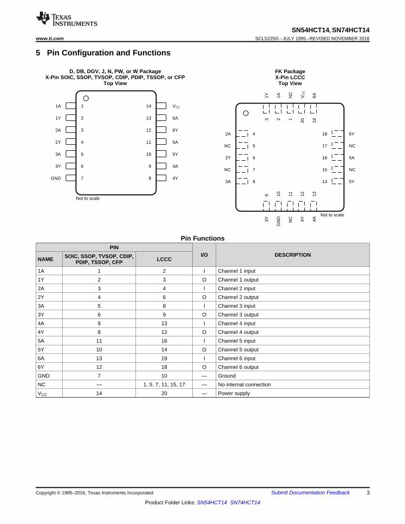
5 Pin Configuration and Functions
D, DB, DGV, J, N, PW, or W PackageX-Pin SOIC, SSOP, TVSOP, CDIP, PDIP, TSSOP, or CFP
Top View
FK PackageX-Pin LCCC
Top View
Pin FunctionsPIN
I/O DESCRIPTIONNAME SOIC, SSOP, TVSOP, CDIP,
PDIP, TSSOP, CFP LCCC
1A 1 2 I Channel 1 input1Y 2 3 O Channel 1 output2A 3 4 I Channel 2 input2Y 4 6 O Channel 2 output3A 5 8 I Channel 3 input3Y 6 9 O Channel 3 output4A 9 13 I Channel 4 input4Y 8 12 O Channel 4 output5A 11 16 I Channel 5 input5Y 10 14 O Channel 5 output6A 13 19 I Channel 6 input6Y 12 18 O Channel 6 outputGND 7 10 — GroundNC — 1, 5, 7, 11, 15, 17 — No internal connectionVCC 14 20 — Power supply
4
SN54HCT14, SN74HCT14SCLS225G –JULY 1995–REVISED NOVEMBER 2016 www.ti.com
Product Folder Links: SN54HCT14 SN74HCT14
Submit Documentation Feedback Copyright © 1995–2016, Texas Instruments Incorporated
(1) Stresses beyond those listed under Absolute Maximum Ratings may cause permanent damage to the device. These are stress ratingsonly, which do not imply functional operation of the device at these or any other conditions beyond those indicated under RecommendedOperating Conditions. Exposure to absolute-maximum-rated conditions for extended periods may affect device reliability.
(2) The input and output voltage ratings may be exceeded if the input and output current ratings are observed.
6 Specifications
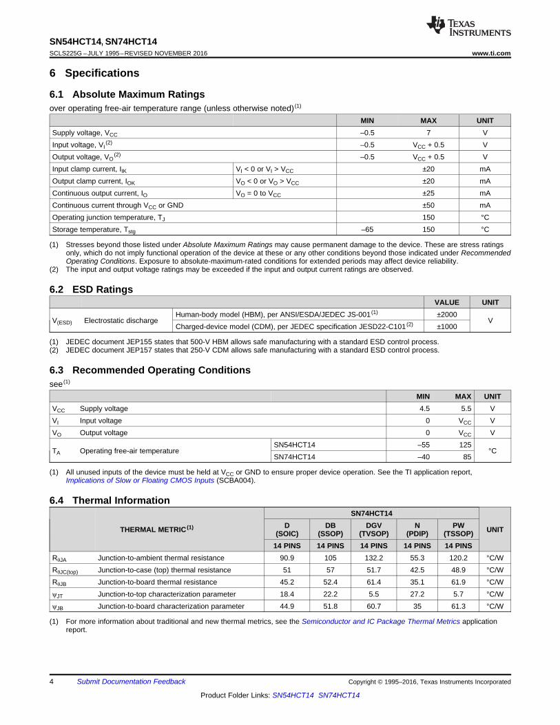
6.1 Absolute Maximum Ratingsover operating free-air temperature range (unless otherwise noted) (1)
MIN MAX UNITSupply voltage, VCC –0.5 7 VInput voltage, VI
(2) –0.5 VCC + 0.5 VOutput voltage, VO
(2) –0.5 VCC + 0.5 VInput clamp current, IIK VI < 0 or VI > VCC ±20 mAOutput clamp current, IOK VO < 0 or VO > VCC ±20 mAContinuous output current, IO VO = 0 to VCC ±25 mAContinuous current through VCC or GND ±50 mAOperating junction temperature, TJ 150 °CStorage temperature, Tstg –65 150 °C
(1) JEDEC document JEP155 states that 500-V HBM allows safe manufacturing with a standard ESD control process.(2) JEDEC document JEP157 states that 250-V CDM allows safe manufacturing with a standard ESD control process.
6.2 ESD RatingsVALUE UNIT
V(ESD) Electrostatic dischargeHuman-body model (HBM), per ANSI/ESDA/JEDEC JS-001 (1) ±2000
VCharged-device model (CDM), per JEDEC specification JESD22-C101 (2) ±1000
(1) All unused inputs of the device must be held at VCC or GND to ensure proper device operation. See the TI application report,Implications of Slow or Floating CMOS Inputs (SCBA004).
6.3 Recommended Operating Conditionssee (1)
MIN MAX UNITVCC Supply voltage 4.5 5.5 VVI Input voltage 0 VCC VVO Output voltage 0 VCC V
TA Operating free-air temperatureSN54HCT14 –55 125
°CSN74HCT14 –40 85
(1) For more information about traditional and new thermal metrics, see the Semiconductor and IC Package Thermal Metrics applicationreport.
6.4 Thermal Information
THERMAL METRIC (1)
SN74HCT14
UNITD(SOIC)
DB(SSOP)
DGV(TVSOP)
N(PDIP)
PW(TSSOP)
14 PINS 14 PINS 14 PINS 14 PINS 14 PINSRθJA Junction-to-ambient thermal resistance 90.9 105 132.2 55.3 120.2 °C/WRθJC(top) Junction-to-case (top) thermal resistance 51 57 51.7 42.5 48.9 °C/WRθJB Junction-to-board thermal resistance 45.2 52.4 61.4 35.1 61.9 °C/WψJT Junction-to-top characterization parameter 18.4 22.2 5.5 27.2 5.7 °C/WψJB Junction-to-board characterization parameter 44.9 51.8 60.7 35 61.3 °C/W
5
SN54HCT14, SN74HCT14www.ti.com SCLS225G –JULY 1995–REVISED NOVEMBER 2016
Product Folder Links: SN54HCT14 SN74HCT14
Submit Documentation FeedbackCopyright © 1995–2016, Texas Instruments Incorporated
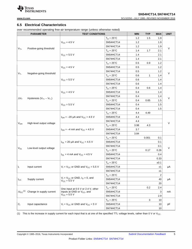
(1) This is the increase in supply current for each input that is at one of the specified TTL voltage levels, rather than 0 V or VCC.
6.5 Electrical Characteristicsover recommended operating free-air temperature range (unless otherwise noted)
PARAMETER TEST CONDITIONS MIN TYP MAX UNIT
VT+ Positive-going threshold
VCC = 4.5 VTA = 25°C 1.2 1.5 1.9
V
SN54HCT14 1.2 1.9SN74HCT14 1.2 1.9
VCC = 5.5 VTA = 25°C 1.4 1.7 2.1SN54HCT14 1.4 2.1SN74HCT14 1.4 2.1
VT– Negative-going threshold
VCC = 4.5 VTA = 25°C 0.5 0.9 1.2
V
SN54HCT14 0.5 1.2SN74HCT14 0.5 1.2
VCC = 5.5 VTA = 25°C 0.6 1 1.4SN54HCT14 0.6 1.4SN74HCT14 0.6 1.4
ΔVT Hysteresis (VT+ – VT–)
VCC = 4.5 VTA = 25°C 0.4 0.6 1.4
V
SN54HCT14 0.4 1.4SN74HCT14 0.4 1.4
VCC = 5.5 VTA = 25°C 0.4 0.65 1.5SN54HCT14 0.4 1.5SN74HCT14 0.4 1.5
VOH High-level output voltage
IOH = –20 µA and VCC = 4.5 VTA = 25°C 4.4 4.49
V
SN54HCT14 4.4SN74HCT14 4.4
IOH = –4 mA and VCC = 4.5 VTA = 25°C 3.98 4.3SN54HCT14 3.7SN74HCT14 3.84
VOL Low-level output voltage
IOL = 20 µA and VCC = 4.5 VTA = 25°C 0.001 0.1
V
SN54HCT14 0.1SN74HCT14 0.1
IOL = 4 mA and VCC = 4.5 VTA = 25°C 0.17 0.26SN54HCT14 0.4SN74HCT14 0.33
II Input current VI = VCC or GND and VCC = 5.5 VTA = 25°C ±0.1
µASN54HCT14 ±1SN74HCT14 ±1
ICC Supply current VI = VCC or GND, IO = 0, andVCC = 5.5 V
TA = 25°C 2µASN54HCT14 40
SN74HCT14 20
ΔICC(1) Change in supply current
One input at 0.5 V or 2.4 V, otherinputs at GND or VCC, andVCC = 5.5 V
TA = 25°C 0.2 2.4mASN54HCT14 3
SN74HCT14 2.9
Ci Input capacitance VI = VCC or GND and VCC = 5 VTA = 25°C 3 10
pFSN54HCT14 10SN74HCT14 10
0.25
0.2
0.1
0.05
0
0.45
0.15
0 0.45 0.9 1.35 1.8 2.26 2.7
−S
up
ply
Cu
rre
nt
−m
A
0.35
0.3
0.4
3.16 3.61 4
V −I Input Voltage − V
I CC
VI = 0 to VCC
VI = VCC to 0
VCC = 4.5 V
0.25
0.2
0.1
0.05
0
0.45
0.15
0 0.55 1.1 1.66 2.2 2.76 3.3
−S
up
ply
Cu
rre
nt
−m
A
0.35
0.3
0.4
3.86 4.4 4.97
V −I Input Voltage − V
I CC
VI = 0 to VCC
VI = VCC to 0
VCC = 5.5 V
6
SN54HCT14, SN74HCT14SCLS225G –JULY 1995–REVISED NOVEMBER 2016 www.ti.com
Product Folder Links: SN54HCT14 SN74HCT14
Submit Documentation Feedback Copyright © 1995–2016, Texas Instruments Incorporated
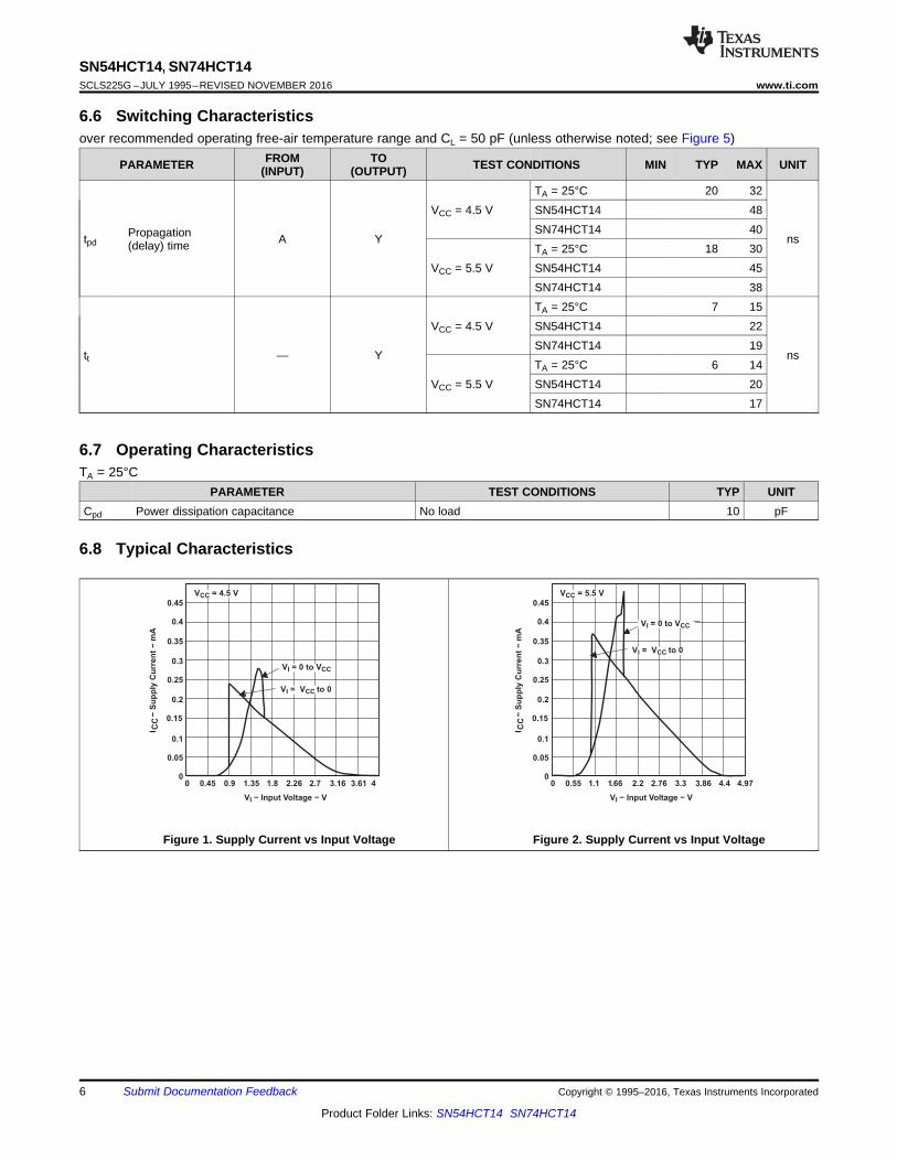
6.6 Switching Characteristicsover recommended operating free-air temperature range and CL = 50 pF (unless otherwise noted; see Figure 5)
PARAMETER FROM(INPUT)
TO(OUTPUT) TEST CONDITIONS MIN TYP MAX UNIT
tpdPropagation(delay) time A Y
VCC = 4.5 VTA = 25°C 20 32
ns
SN54HCT14 48SN74HCT14 40
VCC = 5.5 VTA = 25°C 18 30SN54HCT14 45SN74HCT14 38
tt — Y
VCC = 4.5 VTA = 25°C 7 15
ns
SN54HCT14 22SN74HCT14 19
VCC = 5.5 VTA = 25°C 6 14SN54HCT14 20SN74HCT14 17
6.7 Operating CharacteristicsTA = 25°C
PARAMETER TEST CONDITIONS TYP UNITCpd Power dissipation capacitance No load 10 pF
6.8 Typical Characteristics
Figure 1. Supply Current vs Input Voltage Figure 2. Supply Current vs Input Voltage
VOLTAGE WAVEFORM
INPUT RISE AND FALL TIMES
VOLTAGE WAVEFORMS
PROPAGATION DELAY AND OUTPUT RISE AND FALL TIMES
1.3 V
1.3 V1.3 V10%10%
90% 90%
3 V
VOH
VOL
0 V
tr t
Input
f
In-Phase
Output
1.3 V
tPLH tPHL
1.3 V 1.3 V10% 10%
90%90%VOH
VOL
tt rf
tPHL tPLH
Out-of-Phase
Output
Test
Point
From Output
Under Test
LOAD CIRCUIT
CL = 50 pF
(see Note A)
1.3 V1.3 V10%10%
90% 90%VCC
0 V
tr t
Input
f
0 0.75 1.5 2.27
−O
utp
ut
Vo
lta
ge
−V
3 3.77
6
5
4
3
2
1
0
−1
VO
VI
−
– Input Voltage – V
VI = Down
VI = Up
VCC = 4.5 V
0 0.92 1.84 2.76
−O
utp
ut
Vo
lta
ge
−V
3.68 4.6
6
5
4
3
2
1
0
−1
VO
VI
−
– Input Voltage − V
VI = Down
VI = Up
VCC = 5.5 V
7
SN54HCT14, SN74HCT14www.ti.com SCLS225G –JULY 1995–REVISED NOVEMBER 2016
Product Folder Links: SN54HCT14 SN74HCT14
Submit Documentation FeedbackCopyright © 1995–2016, Texas Instruments Incorporated
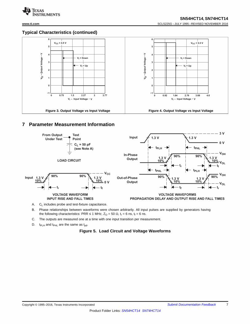
Typical Characteristics (continued)
Figure 3. Output Voltage vs Input Voltage Figure 4. Output Voltage vs Input Voltage
7 Parameter Measurement Information
A. CL includes probe and test-fixture capacitance.B. Phase relationships between waveforms were chosen arbitrarily. All input pulses are supplied by generators having
the following characteristics: PRR ≤ 1 MHz, ZO = 50 Ω, tr = 6 ns, tf = 6 ns.C. The outputs are measured one at a time with one input transition per measurement.D. tPLH and tPHL are the same as tpd.
Figure 5. Load Circuit and Voltage Waveforms
YA
Copyright © 2016, Texas Instruments Incorporated
8
SN54HCT14, SN74HCT14SCLS225G –JULY 1995–REVISED NOVEMBER 2016 www.ti.com
Product Folder Links: SN54HCT14 SN74HCT14
Submit Documentation Feedback Copyright © 1995–2016, Texas Instruments Incorporated
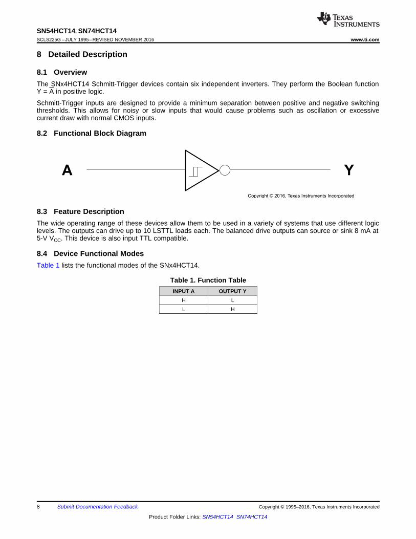
8 Detailed Description
8.1 OverviewThe SNx4HCT14 Schmitt-Trigger devices contain six independent inverters. They perform the Boolean functionY = A in positive logic.
Schmitt-Trigger inputs are designed to provide a minimum separation between positive and negative switchingthresholds. This allows for noisy or slow inputs that would cause problems such as oscillation or excessivecurrent draw with normal CMOS inputs.
8.2 Functional Block Diagram
8.3 Feature DescriptionThe wide operating range of these devices allow them to be used in a variety of systems that use different logiclevels. The outputs can drive up to 10 LSTTL loads each. The balanced drive outputs can source or sink 8 mA at5-V VCC. This device is also input TTL compatible.
8.4 Device Functional ModesTable 1 lists the functional modes of the SNx4HCT14.
Table 1. Function TableINPUT A OUTPUT Y
H LL H
Copyright © 2016, Texas Instruments Incorporated
9
SN54HCT14, SN74HCT14www.ti.com SCLS225G –JULY 1995–REVISED NOVEMBER 2016
Product Folder Links: SN54HCT14 SN74HCT14
Submit Documentation FeedbackCopyright © 1995–2016, Texas Instruments Incorporated
9 Application and Implementation
NOTEInformation in the following applications sections is not part of the TI componentspecification, and TI does not warrant its accuracy or completeness. TI’s customers areresponsible for determining suitability of components for their purposes. Customers shouldvalidate and test their design implementation to confirm system functionality.
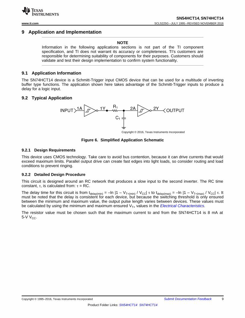
9.1 Application InformationThe SN74HCT14 device is a Schmitt-Trigger input CMOS device that can be used for a multitude of invertingbuffer type functions. The application shown here takes advantage of the Schmitt-Trigger inputs to produce adelay for a logic input.
9.2 Typical Application
Figure 6. Simplified Application Schematic
9.2.1 Design RequirementsThis device uses CMOS technology. Take care to avoid bus contention, because it can drive currents that wouldexceed maximum limits. Parallel output drive can create fast edges into light loads, so consider routing and loadconditions to prevent ringing.
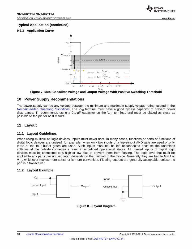
9.2.2 Detailed Design ProcedureThis circuit is designed around an RC network that produces a slow input to the second inverter. The RC timeconstant, τ, is calculated from: τ = RC.
The delay time for this circuit is from tdelay(min) = –ln |1 – VT+(min) / VCC| τ to tdelay(max) = –ln |1 – VT+(max) / VCC| τ. Itmust be noted that the delay is consistent for each device, but because the switching threshold is only ensuredbetween the minimum and maximum value, the output pulse length varies between devices. These values mustbe calculated by using the minimum and maximum ensured VT+ values in the Electrical Characteristics.
The resistor value must be chosen such that the maximum current to and from the SN74HCT14 is 8 mA at5-V VCC.
Vcc
Unused Input
Input
Output
Input
Unused Input Output
VC
VOUT
t0 + 2�t0 t0 + 52�
Vol
tage
Time
0.0t0 + 22� t0 + 32� t0 + 42�
VT
+
VT+ Typical
VCC
VT+(min)
VT+(max)
W|1|ln (max)(max)
CC
Tdelay V
Vt �
��
W|1|ln (min)(min)
CC
Tdelay V
Vt �
��
10
SN54HCT14, SN74HCT14SCLS225G –JULY 1995–REVISED NOVEMBER 2016 www.ti.com
Product Folder Links: SN54HCT14 SN74HCT14
Submit Documentation Feedback Copyright © 1995–2016, Texas Instruments Incorporated
Typical Application (continued)9.2.3 Application Curve
Figure 7. Ideal Capacitor Voltage and Output Voltage With Positive Switching Threshold
10 Power Supply RecommendationsThe power supply can be any voltage between the minimum and maximum supply voltage rating located in theRecommended Operating Conditions. The VCC terminal must have a good bypass capacitor to prevent powerdisturbance. TI recommends using a 0.1-µF capacitor on the VCC terminal, and must be placed as close aspossible to the pin for best results.
11 Layout
11.1 Layout GuidelinesWhen using multiple bit logic devices, inputs must never float. In many cases, functions or parts of functions ofdigital logic devices are unused, for example, when only two inputs of a triple-input AND gate are used or onlythree of the four buffer gates are used. Such inputs must not be left unconnected because the undefinedvoltages at the outside connections result in undefined operational states. All unused inputs of digital logicdevices must be connected to a high or low bias to prevent them from floating. The logic level that must beapplied to any particular unused input depends on the function of the device. Generally they are tied to GND orVCC, whichever makes more sense or is more convenient. Floating outputs are generally acceptable, unless thepart is a transceiver.
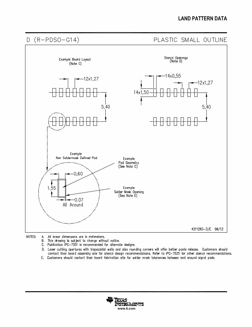
11.2 Layout Example
Figure 8. Layout Diagram
11
SN54HCT14, SN74HCT14www.ti.com SCLS225G –JULY 1995–REVISED NOVEMBER 2016
Product Folder Links: SN54HCT14 SN74HCT14
Submit Documentation FeedbackCopyright © 1995–2016, Texas Instruments Incorporated
12 Device and Documentation Support
12.1 Documentation Support
12.1.1 Related DocumentationFor related documentation see the following:
Implications of Slow or Floating CMOS Inputs (SCBA004)
12.2 Related LinksThe table below lists quick access links. Categories include technical documents, support and communityresources, tools and software, and quick access to sample or buy.
Table 2. Related Links
PARTS PRODUCT FOLDER SAMPLE & BUY TECHNICALDOCUMENTS
TOOLS &SOFTWARE
SUPPORT &COMMUNITY
SN54HCT14 Click here Click here Click here Click here Click hereSN74HCT14 Click here Click here Click here Click here Click here
12.3 Receiving Notification of Documentation UpdatesTo receive notification of documentation updates, navigate to the device product folder on ti.com. In the upperright corner, click on Alert me to register and receive a weekly digest of any product information that haschanged. For change details, review the revision history included in any revised document.
12.4 Community ResourceThe following links connect to TI community resources. Linked contents are provided "AS IS" by the respectivecontributors. They do not constitute TI specifications and do not necessarily reflect TI's views; see TI's Terms ofUse.
TI E2E™ Online Community TI's Engineer-to-Engineer (E2E) Community. Created to foster collaborationamong engineers. At e2e.ti.com, you can ask questions, share knowledge, explore ideas and helpsolve problems with fellow engineers.
Design Support TI's Design Support Quickly find helpful E2E forums along with design support tools andcontact information for technical support.
12.5 TrademarksE2E is a trademark of Texas Instruments.All other trademarks are the property of their respective owners.
12.6 Electrostatic Discharge CautionThese devices have limited built-in ESD protection. The leads should be shorted together or the device placed in conductive foamduring storage or handling to prevent electrostatic damage to the MOS gates.
12.7 GlossarySLYZ022 — TI Glossary.
This glossary lists and explains terms, acronyms, and definitions.
13 Mechanical, Packaging, and Orderable InformationThe following pages include mechanical, packaging, and orderable information. This information is the mostcurrent data available for the designated devices. This data is subject to change without notice and revision ofthis document. For browser-based versions of this data sheet, refer to the left-hand navigation.
PACKAGE OPTION ADDENDUM
www.ti.com 17-Mar-2017
Addendum-Page 1
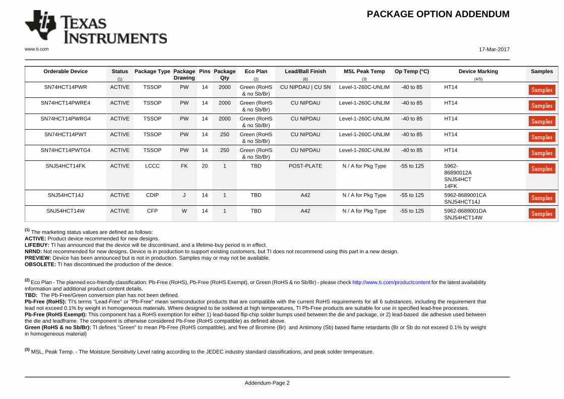
PACKAGING INFORMATION
Orderable Device Status(1)
Package Type PackageDrawing
Pins PackageQty
Eco Plan(2)
Lead/Ball Finish(6)
MSL Peak Temp(3)
Op Temp (°C) Device Marking(4/5)
Samples
5962-86890012A ACTIVE LCCC FK 20 1 TBD POST-PLATE N / A for Pkg Type -55 to 125 5962-86890012ASNJ54HCT14FK
5962-8689001CA ACTIVE CDIP J 14 1 TBD A42 N / A for Pkg Type -55 to 125 5962-8689001CASNJ54HCT14J
5962-8689001DA ACTIVE CFP W 14 1 TBD A42 N / A for Pkg Type -55 to 125 5962-8689001DASNJ54HCT14W
SN74HCT14D ACTIVE SOIC D 14 50 Green (RoHS& no Sb/Br)
CU NIPDAU Level-1-260C-UNLIM -40 to 85 HCT14
SN74HCT14DBR ACTIVE SSOP DB 14 2000 Green (RoHS& no Sb/Br)
CU NIPDAU Level-1-260C-UNLIM -40 to 85 HT14
SN74HCT14DE4 ACTIVE SOIC D 14 50 Green (RoHS& no Sb/Br)
CU NIPDAU Level-1-260C-UNLIM -40 to 85 HCT14
SN74HCT14DG4 ACTIVE SOIC D 14 50 Green (RoHS& no Sb/Br)
CU NIPDAU Level-1-260C-UNLIM -40 to 85 HCT14
SN74HCT14DGVR ACTIVE TVSOP DGV 14 2000 Green (RoHS& no Sb/Br)
CU NIPDAU Level-1-260C-UNLIM -40 to 85 HT14
SN74HCT14DR ACTIVE SOIC D 14 2500 Green (RoHS& no Sb/Br)
CU NIPDAU | CU SN Level-1-260C-UNLIM -40 to 85 HCT14
SN74HCT14DRE4 ACTIVE SOIC D 14 2500 Green (RoHS& no Sb/Br)
CU NIPDAU Level-1-260C-UNLIM -40 to 85 HCT14
SN74HCT14DRG3 ACTIVE SOIC D 14 2500 Green (RoHS& no Sb/Br)
CU SN Level-1-260C-UNLIM -40 to 85 HCT14
SN74HCT14DRG4 ACTIVE SOIC D 14 2500 Green (RoHS& no Sb/Br)
CU NIPDAU Level-1-260C-UNLIM -40 to 85 HCT14
SN74HCT14DT ACTIVE SOIC D 14 250 Green (RoHS& no Sb/Br)
CU NIPDAU Level-1-260C-UNLIM -40 to 85 HCT14
SN74HCT14DTG4 ACTIVE SOIC D 14 250 Green (RoHS& no Sb/Br)
CU NIPDAU Level-1-260C-UNLIM -40 to 85 HCT14
SN74HCT14N ACTIVE PDIP N 14 25 Pb-Free(RoHS)
CU NIPDAU N / A for Pkg Type -40 to 85 SN74HCT14N
SN74HCT14NE4 ACTIVE PDIP N 14 25 Pb-Free(RoHS)
CU NIPDAU N / A for Pkg Type -40 to 85 SN74HCT14N
PACKAGE OPTION ADDENDUM
www.ti.com 17-Mar-2017
Addendum-Page 2
Orderable Device Status(1)
Package Type PackageDrawing
Pins PackageQty
Eco Plan(2)
Lead/Ball Finish(6)
MSL Peak Temp(3)
Op Temp (°C) Device Marking(4/5)
Samples
SN74HCT14PWR ACTIVE TSSOP PW 14 2000 Green (RoHS& no Sb/Br)
CU NIPDAU | CU SN Level-1-260C-UNLIM -40 to 85 HT14
SN74HCT14PWRE4 ACTIVE TSSOP PW 14 2000 Green (RoHS& no Sb/Br)
CU NIPDAU Level-1-260C-UNLIM -40 to 85 HT14
SN74HCT14PWRG4 ACTIVE TSSOP PW 14 2000 Green (RoHS& no Sb/Br)
CU NIPDAU Level-1-260C-UNLIM -40 to 85 HT14
SN74HCT14PWT ACTIVE TSSOP PW 14 250 Green (RoHS& no Sb/Br)
CU NIPDAU Level-1-260C-UNLIM -40 to 85 HT14
SN74HCT14PWTG4 ACTIVE TSSOP PW 14 250 Green (RoHS& no Sb/Br)
CU NIPDAU Level-1-260C-UNLIM -40 to 85 HT14
SNJ54HCT14FK ACTIVE LCCC FK 20 1 TBD POST-PLATE N / A for Pkg Type -55 to 125 5962-86890012ASNJ54HCT14FK
SNJ54HCT14J ACTIVE CDIP J 14 1 TBD A42 N / A for Pkg Type -55 to 125 5962-8689001CASNJ54HCT14J
SNJ54HCT14W ACTIVE CFP W 14 1 TBD A42 N / A for Pkg Type -55 to 125 5962-8689001DASNJ54HCT14W
(1) The marketing status values are defined as follows:ACTIVE: Product device recommended for new designs.LIFEBUY: TI has announced that the device will be discontinued, and a lifetime-buy period is in effect.NRND: Not recommended for new designs. Device is in production to support existing customers, but TI does not recommend using this part in a new design.PREVIEW: Device has been announced but is not in production. Samples may or may not be available.OBSOLETE: TI has discontinued the production of the device.
(2) Eco Plan - The planned eco-friendly classification: Pb-Free (RoHS), Pb-Free (RoHS Exempt), or Green (RoHS & no Sb/Br) - please check http://www.ti.com/productcontent for the latest availabilityinformation and additional product content details.TBD: The Pb-Free/Green conversion plan has not been defined.Pb-Free (RoHS): TI's terms "Lead-Free" or "Pb-Free" mean semiconductor products that are compatible with the current RoHS requirements for all 6 substances, including the requirement thatlead not exceed 0.1% by weight in homogeneous materials. Where designed to be soldered at high temperatures, TI Pb-Free products are suitable for use in specified lead-free processes.Pb-Free (RoHS Exempt): This component has a RoHS exemption for either 1) lead-based flip-chip solder bumps used between the die and package, or 2) lead-based die adhesive used betweenthe die and leadframe. The component is otherwise considered Pb-Free (RoHS compatible) as defined above.Green (RoHS & no Sb/Br): TI defines "Green" to mean Pb-Free (RoHS compatible), and free of Bromine (Br) and Antimony (Sb) based flame retardants (Br or Sb do not exceed 0.1% by weightin homogeneous material)
(3) MSL, Peak Temp. - The Moisture Sensitivity Level rating according to the JEDEC industry standard classifications, and peak solder temperature.
PACKAGE OPTION ADDENDUM
www.ti.com 17-Mar-2017
Addendum-Page 3
(4) There may be additional marking, which relates to the logo, the lot trace code information, or the environmental category on the device.
(5) Multiple Device Markings will be inside parentheses. Only one Device Marking contained in parentheses and separated by a "~" will appear on a device. If a line is indented then it is a continuationof the previous line and the two combined represent the entire Device Marking for that device.
(6) Lead/Ball Finish - Orderable Devices may have multiple material finish options. Finish options are separated by a vertical ruled line. Lead/Ball Finish values may wrap to two lines if the finishvalue exceeds the maximum column width.
Important Information and Disclaimer:The information provided on this page represents TI's knowledge and belief as of the date that it is provided. TI bases its knowledge and belief on informationprovided by third parties, and makes no representation or warranty as to the accuracy of such information. Efforts are underway to better integrate information from third parties. TI has taken andcontinues to take reasonable steps to provide representative and accurate information but may not have conducted destructive testing or chemical analysis on incoming materials and chemicals.TI and TI suppliers consider certain information to be proprietary, and thus CAS numbers and other limited information may not be available for release.
In no event shall TI's liability arising out of such information exceed the total purchase price of the TI part(s) at issue in this document sold by TI to Customer on an annual basis.
OTHER QUALIFIED VERSIONS OF SN54HCT14, SN74HCT14 :
• Catalog: SN74HCT14
• Automotive: SN74HCT14-Q1, SN74HCT14-Q1
• Military: SN54HCT14
NOTE: Qualified Version Definitions:
• Catalog - TI's standard catalog product
• Automotive - Q100 devices qualified for high-reliability automotive applications targeting zero defects
• Military - QML certified for Military and Defense Applications
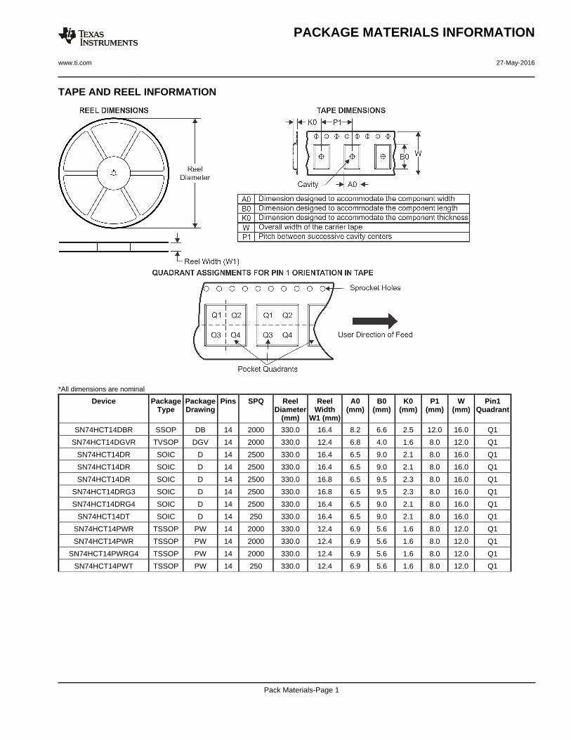
TAPE AND REEL INFORMATION
*All dimensions are nominal
Device PackageType
PackageDrawing
Pins SPQ ReelDiameter
(mm)
ReelWidth
W1 (mm)
A0(mm)
B0(mm)
K0(mm)
P1(mm)
W(mm)
Pin1Quadrant
SN74HCT14DBR SSOP DB 14 2000 330.0 16.4 8.2 6.6 2.5 12.0 16.0 Q1
SN74HCT14DGVR TVSOP DGV 14 2000 330.0 12.4 6.8 4.0 1.6 8.0 12.0 Q1
SN74HCT14DR SOIC D 14 2500 330.0 16.4 6.5 9.0 2.1 8.0 16.0 Q1
SN74HCT14DR SOIC D 14 2500 330.0 16.4 6.5 9.0 2.1 8.0 16.0 Q1
SN74HCT14DR SOIC D 14 2500 330.0 16.8 6.5 9.5 2.3 8.0 16.0 Q1
SN74HCT14DRG3 SOIC D 14 2500 330.0 16.8 6.5 9.5 2.3 8.0 16.0 Q1
SN74HCT14DRG4 SOIC D 14 2500 330.0 16.4 6.5 9.0 2.1 8.0 16.0 Q1
SN74HCT14DT SOIC D 14 250 330.0 16.4 6.5 9.0 2.1 8.0 16.0 Q1
SN74HCT14PWR TSSOP PW 14 2000 330.0 12.4 6.9 5.6 1.6 8.0 12.0 Q1
SN74HCT14PWR TSSOP PW 14 2000 330.0 12.4 6.9 5.6 1.6 8.0 12.0 Q1
SN74HCT14PWRG4 TSSOP PW 14 2000 330.0 12.4 6.9 5.6 1.6 8.0 12.0 Q1
SN74HCT14PWT TSSOP PW 14 250 330.0 12.4 6.9 5.6 1.6 8.0 12.0 Q1
PACKAGE MATERIALS INFORMATION
www.ti.com 27-May-2016
Pack Materials-Page 1
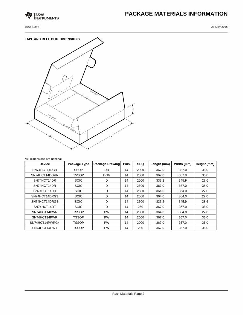
*All dimensions are nominal
Device Package Type Package Drawing Pins SPQ Length (mm) Width (mm) Height (mm)
SN74HCT14DBR SSOP DB 14 2000 367.0 367.0 38.0
SN74HCT14DGVR TVSOP DGV 14 2000 367.0 367.0 35.0
SN74HCT14DR SOIC D 14 2500 333.2 345.9 28.6
SN74HCT14DR SOIC D 14 2500 367.0 367.0 38.0
SN74HCT14DR SOIC D 14 2500 364.0 364.0 27.0
SN74HCT14DRG3 SOIC D 14 2500 364.0 364.0 27.0
SN74HCT14DRG4 SOIC D 14 2500 333.2 345.9 28.6
SN74HCT14DT SOIC D 14 250 367.0 367.0 38.0
SN74HCT14PWR TSSOP PW 14 2000 364.0 364.0 27.0
SN74HCT14PWR TSSOP PW 14 2000 367.0 367.0 35.0
SN74HCT14PWRG4 TSSOP PW 14 2000 367.0 367.0 35.0
SN74HCT14PWT TSSOP PW 14 250 367.0 367.0 35.0
PACKAGE MATERIALS INFORMATION
www.ti.com 27-May-2016
Pack Materials-Page 2
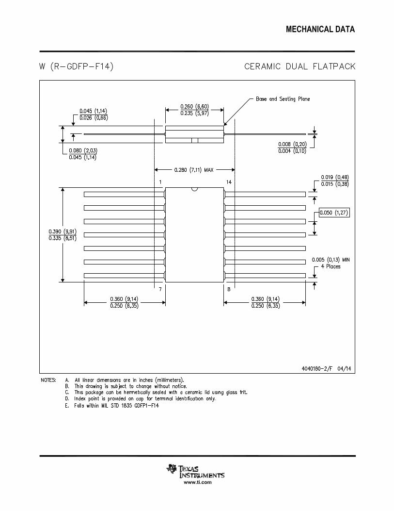
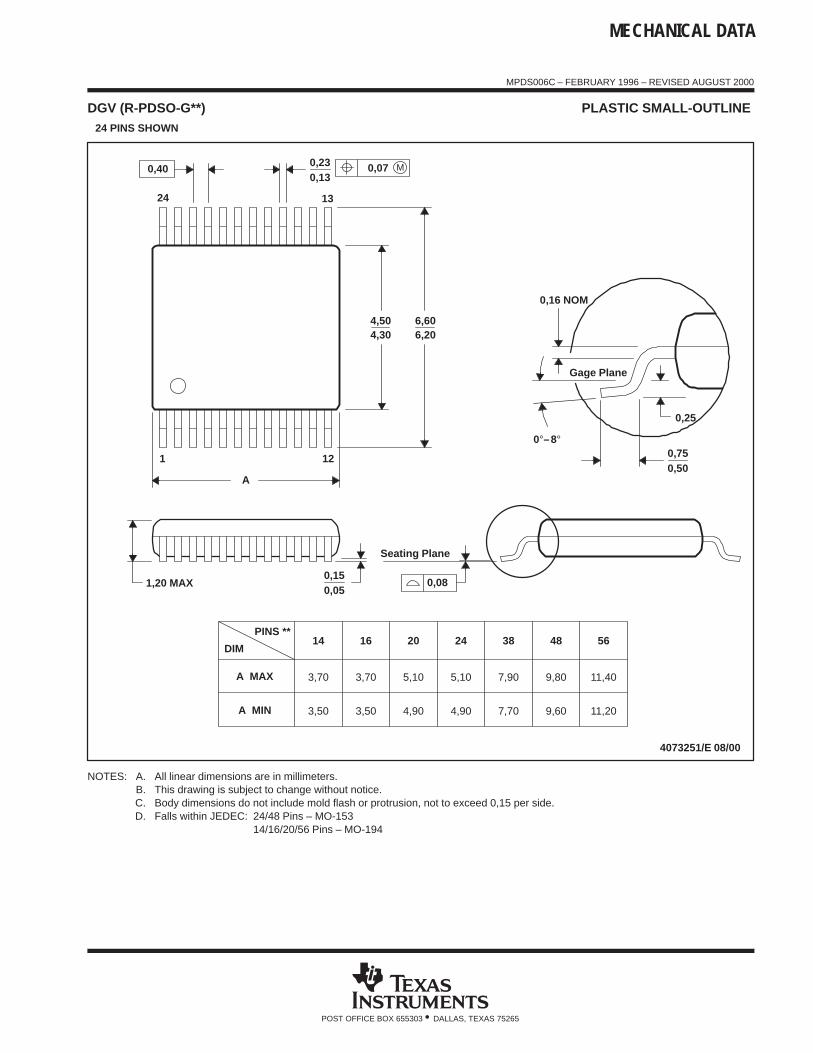
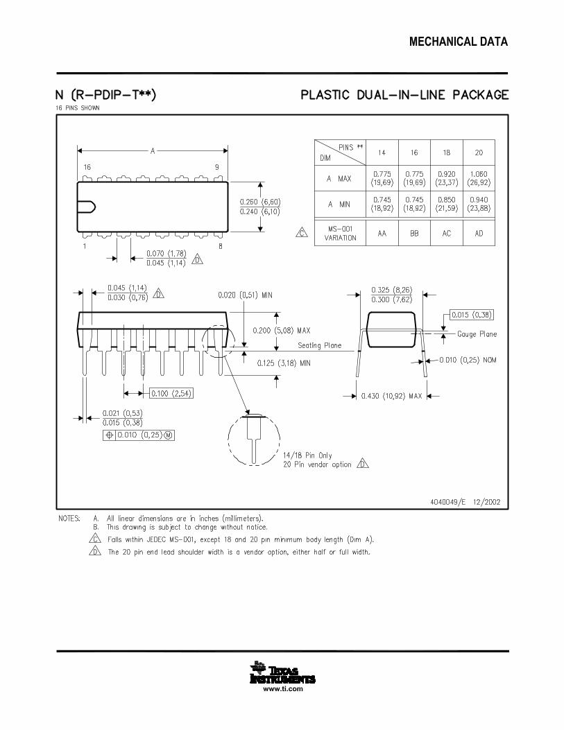
MECHANICAL DATA
MPDS006C – FEBRUARY 1996 – REVISED AUGUST 2000
POST OFFICE BOX 655303 • DALLAS, TEXAS 75265
DGV (R-PDSO-G**) PLASTIC SMALL-OUTLINE 24 PINS SHOWN
14
3,70
3,50 4,90
5,10
20DIM
PINS **
4073251/E 08/00
1,20 MAX
Seating Plane
0,050,15
0,25
0,500,75
0,230,13
1 12
24 13
4,304,50
0,16 NOM
Gage Plane
A
7,90
7,70
382416
4,90
5,103,70
3,50
A MAX
A MIN
6,606,20
11,20
11,40
56
9,60
9,80
48
0,08
M0,070,40
0°–�8°
NOTES: A. All linear dimensions are in millimeters.B. This drawing is subject to change without notice.C. Body dimensions do not include mold flash or protrusion, not to exceed 0,15 per side.D. Falls within JEDEC: 24/48 Pins – MO-153
14/16/20/56 Pins – MO-194
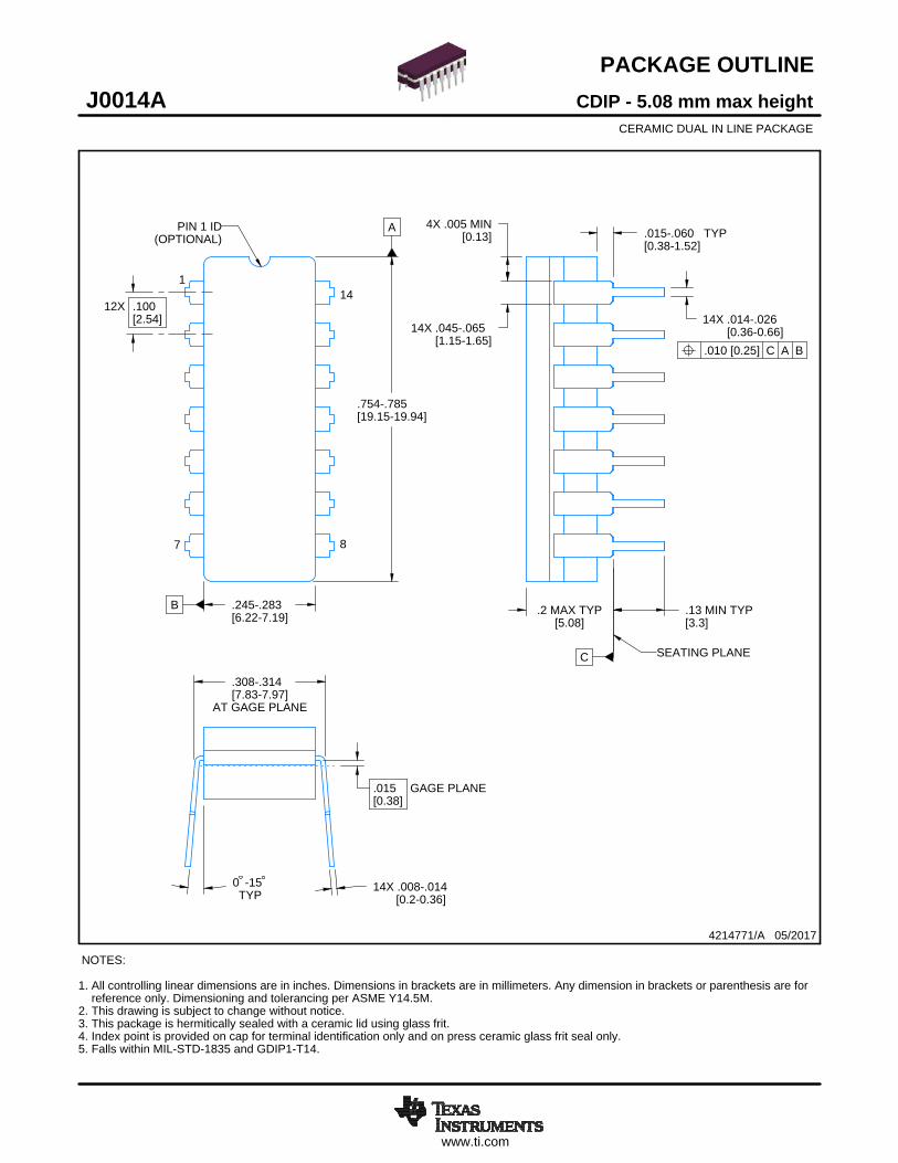
www.ti.com
PACKAGE OUTLINE
C
14X .008-.014 [0.2-0.36]TYP
-150
AT GAGE PLANE
-.314.308-7.977.83[ ]
14X -.026.014-0.660.36[ ]14X -.065.045
-1.651.15[ ]
.2 MAX TYP[5.08]
.13 MIN TYP[3.3]
TYP-.060.015-1.520.38[ ]
4X .005 MIN[0.13]
12X .100[2.54]
.015 GAGE PLANE[0.38]
A
-.785.754-19.9419.15[ ]
B -.283.245-7.196.22[ ]
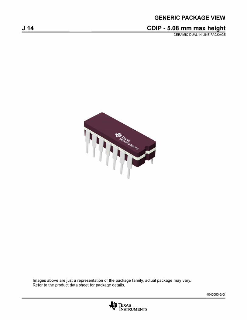
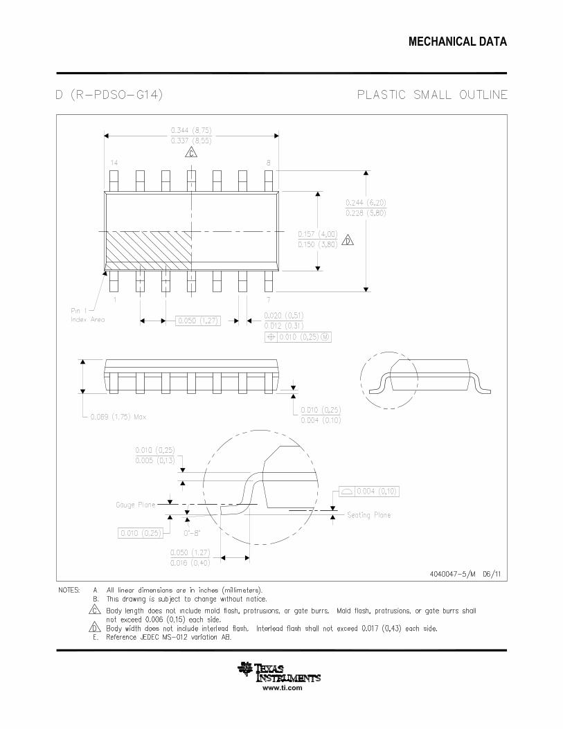
CDIP - 5.08 mm max heightJ0014ACERAMIC DUAL IN LINE PACKAGE
4214771/A 05/2017
NOTES: 1. All controlling linear dimensions are in inches. Dimensions in brackets are in millimeters. Any dimension in brackets or parenthesis are for reference only. Dimensioning and tolerancing per ASME Y14.5M.2. This drawing is subject to change without notice. 3. This package is hermitically sealed with a ceramic lid using glass frit.4. Index point is provided on cap for terminal identification only and on press ceramic glass frit seal only.5. Falls within MIL-STD-1835 and GDIP1-T14.
7 8
141
PIN 1 ID(OPTIONAL)
SCALE 0.900
SEATING PLANE
.010 [0.25] C A B
www.ti.com
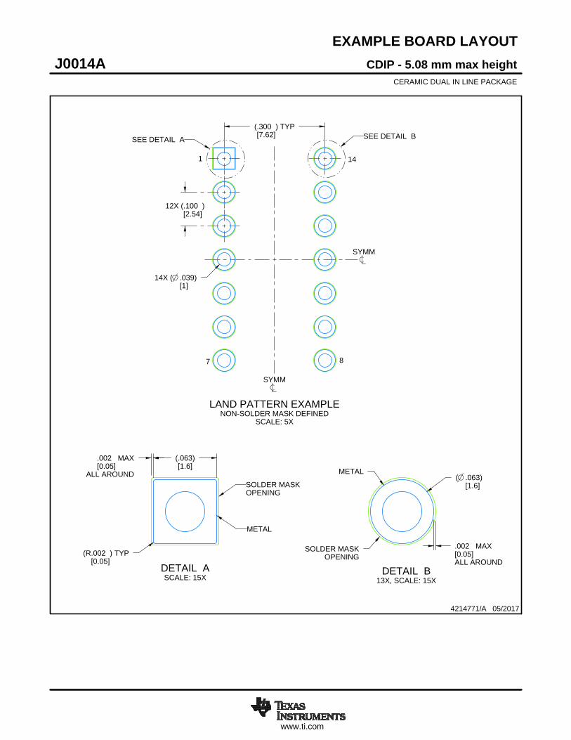
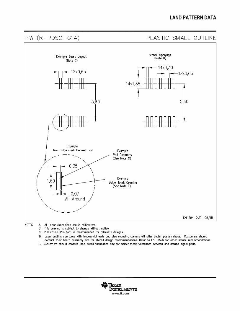
EXAMPLE BOARD LAYOUT
ALL AROUND[0.05]
MAX.002
.002 MAX[0.05]ALL AROUND
SOLDER MASKOPENING
METAL
(.063)[1.6]
(R.002 ) TYP[0.05]
14X ( .039)[1]
( .063)[1.6]
12X (.100 )[2.54]
(.300 ) TYP[7.62]
CDIP - 5.08 mm max heightJ0014ACERAMIC DUAL IN LINE PACKAGE
4214771/A 05/2017
LAND PATTERN EXAMPLENON-SOLDER MASK DEFINED
SCALE: 5X
SEE DETAIL A SEE DETAIL B
SYMM
SYMM
1
7 8
14
DETAIL ASCALE: 15X
SOLDER MASKOPENING
METAL
DETAIL B13X, SCALE: 15X
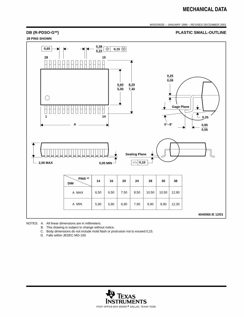
MECHANICAL DATA
MSSO002E – JANUARY 1995 – REVISED DECEMBER 2001
POST OFFICE BOX 655303 • DALLAS, TEXAS 75265
DB (R-PDSO-G**) PLASTIC SMALL-OUTLINE
4040065 /E 12/01
28 PINS SHOWN
Gage Plane
8,207,40
0,550,95
0,25
38
12,90
12,30
28
10,50
24
8,50
Seating Plane
9,907,90
30
10,50
9,90
0,38
5,605,00
15
0,22
14
A
28
1
2016
6,506,50
14
0,05 MIN
5,905,90
DIM
A MAX
A MIN
PINS **
2,00 MAX
6,90
7,50
0,65 M0,15
0°–�8°
0,10
0,090,25
NOTES: A. All linear dimensions are in millimeters.B. This drawing is subject to change without notice.C. Body dimensions do not include mold flash or protrusion not to exceed 0,15.D. Falls within JEDEC MO-150
IMPORTANT NOTICE
Texas Instruments Incorporated (TI) reserves the right to make corrections, enhancements, improvements and other changes to itssemiconductor products and services per JESD46, latest issue, and to discontinue any product or service per JESD48, latest issue. Buyersshould obtain the latest relevant information before placing orders and should verify that such information is current and complete.TI’s published terms of sale for semiconductor products (http://www.ti.com/sc/docs/stdterms.htm) apply to the sale of packaged integratedcircuit products that TI has qualified and released to market. Additional terms may apply to the use or sale of other types of TI products andservices.Reproduction of significant portions of TI information in TI data sheets is permissible only if reproduction is without alteration and isaccompanied by all associated warranties, conditions, limitations, and notices. TI is not responsible or liable for such reproduceddocumentation. Information of third parties may be subject to additional restrictions. Resale of TI products or services with statementsdifferent from or beyond the parameters stated by TI for that product or service voids all express and any implied warranties for theassociated TI product or service and is an unfair and deceptive business practice. TI is not responsible or liable for any such statements.Buyers and others who are developing systems that incorporate TI products (collectively, “Designers”) understand and agree that Designersremain responsible for using their independent analysis, evaluation and judgment in designing their applications and that Designers havefull and exclusive responsibility to assure the safety of Designers' applications and compliance of their applications (and of all TI productsused in or for Designers’ applications) with all applicable regulations, laws and other applicable requirements. Designer represents that, withrespect to their applications, Designer has all the necessary expertise to create and implement safeguards that (1) anticipate dangerousconsequences of failures, (2) monitor failures and their consequences, and (3) lessen the likelihood of failures that might cause harm andtake appropriate actions. Designer agrees that prior to using or distributing any applications that include TI products, Designer willthoroughly test such applications and the functionality of such TI products as used in such applications.TI’s provision of technical, application or other design advice, quality characterization, reliability data or other services or information,including, but not limited to, reference designs and materials relating to evaluation modules, (collectively, “TI Resources”) are intended toassist designers who are developing applications that incorporate TI products; by downloading, accessing or using TI Resources in anyway, Designer (individually or, if Designer is acting on behalf of a company, Designer’s company) agrees to use any particular TI Resourcesolely for this purpose and subject to the terms of this Notice.TI’s provision of TI Resources does not expand or otherwise alter TI’s applicable published warranties or warranty disclaimers for TIproducts, and no additional obligations or liabilities arise from TI providing such TI Resources. TI reserves the right to make corrections,enhancements, improvements and other changes to its TI Resources. TI has not conducted any testing other than that specificallydescribed in the published documentation for a particular TI Resource.Designer is authorized to use, copy and modify any individual TI Resource only in connection with the development of applications thatinclude the TI product(s) identified in such TI Resource. NO OTHER LICENSE, EXPRESS OR IMPLIED, BY ESTOPPEL OR OTHERWISETO ANY OTHER TI INTELLECTUAL PROPERTY RIGHT, AND NO LICENSE TO ANY TECHNOLOGY OR INTELLECTUAL PROPERTYRIGHT OF TI OR ANY THIRD PARTY IS GRANTED HEREIN, including but not limited to any patent right, copyright, mask work right, orother intellectual property right relating to any combination, machine, or process in which TI products or services are used. Informationregarding or referencing third-party products or services does not constitute a license to use such products or services, or a warranty orendorsement thereof. Use of TI Resources may require a license from a third party under the patents or other intellectual property of thethird party, or a license from TI under the patents or other intellectual property of TI.TI RESOURCES ARE PROVIDED “AS IS” AND WITH ALL FAULTS. TI DISCLAIMS ALL OTHER WARRANTIES ORREPRESENTATIONS, EXPRESS OR IMPLIED, REGARDING RESOURCES OR USE THEREOF, INCLUDING BUT NOT LIMITED TOACCURACY OR COMPLETENESS, TITLE, ANY EPIDEMIC FAILURE WARRANTY AND ANY IMPLIED WARRANTIES OFMERCHANTABILITY, FITNESS FOR A PARTICULAR PURPOSE, AND NON-INFRINGEMENT OF ANY THIRD PARTY INTELLECTUALPROPERTY RIGHTS. TI SHALL NOT BE LIABLE FOR AND SHALL NOT DEFEND OR INDEMNIFY DESIGNER AGAINST ANY CLAIM,INCLUDING BUT NOT LIMITED TO ANY INFRINGEMENT CLAIM THAT RELATES TO OR IS BASED ON ANY COMBINATION OFPRODUCTS EVEN IF DESCRIBED IN TI RESOURCES OR OTHERWISE. IN NO EVENT SHALL TI BE LIABLE FOR ANY ACTUAL,DIRECT, SPECIAL, COLLATERAL, INDIRECT, PUNITIVE, INCIDENTAL, CONSEQUENTIAL OR EXEMPLARY DAMAGES INCONNECTION WITH OR ARISING OUT OF TI RESOURCES OR USE THEREOF, AND REGARDLESS OF WHETHER TI HAS BEENADVISED OF THE POSSIBILITY OF SUCH DAMAGES.Unless TI has explicitly designated an individual product as meeting the requirements of a particular industry standard (e.g., ISO/TS 16949and ISO 26262), TI is not responsible for any failure to meet such industry standard requirements.Where TI specifically promotes products as facilitating functional safety or as compliant with industry functional safety standards, suchproducts are intended to help enable customers to design and create their own applications that meet applicable functional safety standardsand requirements. Using products in an application does not by itself establish any safety features in the application. Designers mustensure compliance with safety-related requirements and standards applicable to their applications. Designer may not use any TI products inlife-critical medical equipment unless authorized officers of the parties have executed a special contract specifically governing such use.Life-critical medical equipment is medical equipment where failure of such equipment would cause serious bodily injury or death (e.g., lifesupport, pacemakers, defibrillators, heart pumps, neurostimulators, and implantables). Such equipment includes, without limitation, allmedical devices identified by the U.S. Food and Drug Administration as Class III devices and equivalent classifications outside the U.S.TI may expressly designate certain products as completing a particular qualification (e.g., Q100, Military Grade, or Enhanced Product).Designers agree that it has the necessary expertise to select the product with the appropriate qualification designation for their applicationsand that proper product selection is at Designers’ own risk. Designers are solely responsible for compliance with all legal and regulatoryrequirements in connection with such selection.Designer will fully indemnify TI and its representatives against any damages, costs, losses, and/or liabilities arising out of Designer’s non-compliance with the terms and provisions of this Notice.
Mailing Address: Texas Instruments, Post Office Box 655303, Dallas, Texas 75265Copyright © 2017, Texas Instruments Incorporated