Embed Size (px)
Citation preview
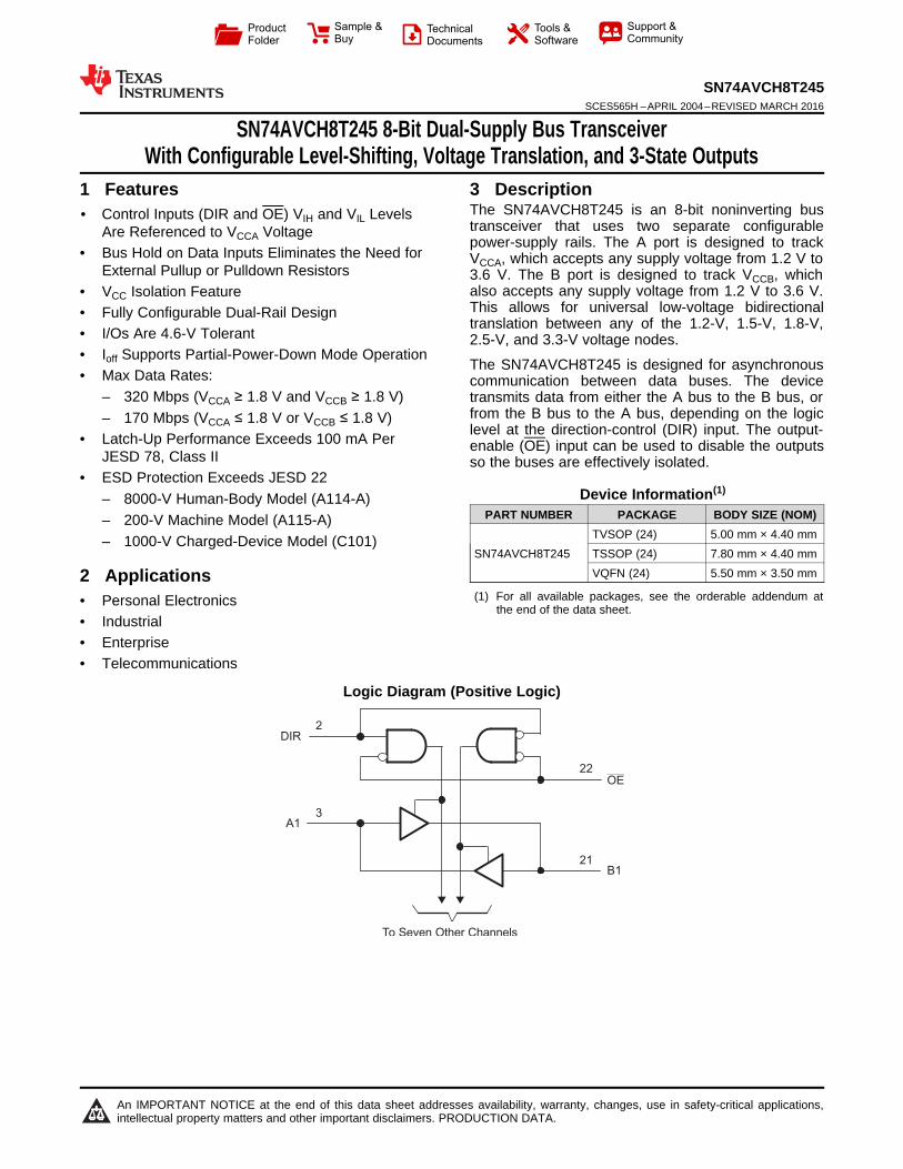
DIR
OE
A1
B1
To Seven Other Channels
2
3
22
21
Product
Folder
Sample &Buy
Technical
Documents
Tools &
Software
Support &Community
An IMPORTANT NOTICE at the end of this data sheet addresses availability, warranty, changes, use in safety-critical applications,intellectual property matters and other important disclaimers. PRODUCTION DATA.
SN74AVCH8T245SCES565H –APRIL 2004–REVISED MARCH 2016
SN74AVCH8T245 8-Bit Dual-Supply Bus TransceiverWith Configurable Level-Shifting, Voltage Translation, and 3-State Outputs
1
1 Features1• Control Inputs (DIR and OE) VIH and VIL Levels
Are Referenced to VCCA Voltage• Bus Hold on Data Inputs Eliminates the Need for
External Pullup or Pulldown Resistors• VCC Isolation Feature• Fully Configurable Dual-Rail Design• I/Os Are 4.6-V Tolerant• Ioff Supports Partial-Power-Down Mode Operation• Max Data Rates:
– 320 Mbps (VCCA ≥ 1.8 V and VCCB ≥ 1.8 V)– 170 Mbps (VCCA ≤ 1.8 V or VCCB ≤ 1.8 V)
• Latch-Up Performance Exceeds 100 mA PerJESD 78, Class II
• ESD Protection Exceeds JESD 22– 8000-V Human-Body Model (A114-A)– 200-V Machine Model (A115-A)– 1000-V Charged-Device Model (C101)
2 Applications• Personal Electronics• Industrial• Enterprise• Telecommunications
3 DescriptionThe SN74AVCH8T245 is an 8-bit noninverting bustransceiver that uses two separate configurablepower-supply rails. The A port is designed to trackVCCA, which accepts any supply voltage from 1.2 V to3.6 V. The B port is designed to track VCCB, whichalso accepts any supply voltage from 1.2 V to 3.6 V.This allows for universal low-voltage bidirectionaltranslation between any of the 1.2-V, 1.5-V, 1.8-V,2.5-V, and 3.3-V voltage nodes.
The SN74AVCH8T245 is designed for asynchronouscommunication between data buses. The devicetransmits data from either the A bus to the B bus, orfrom the B bus to the A bus, depending on the logiclevel at the direction-control (DIR) input. The output-enable (OE) input can be used to disable the outputsso the buses are effectively isolated.
Device Information(1)
PART NUMBER PACKAGE BODY SIZE (NOM)
SN74AVCH8T245TVSOP (24) 5.00 mm × 4.40 mmTSSOP (24) 7.80 mm × 4.40 mmVQFN (24) 5.50 mm × 3.50 mm
(1) For all available packages, see the orderable addendum atthe end of the data sheet.
Logic Diagram (Positive Logic)
2
SN74AVCH8T245SCES565H –APRIL 2004–REVISED MARCH 2016 www.ti.com
Product Folder Links: SN74AVCH8T245
Submit Documentation Feedback Copyright © 2004–2016, Texas Instruments Incorporated
Table of Contents1 Features .................................................................. 12 Applications ........................................................... 13 Description ............................................................. 14 Revision History..................................................... 25 Description (continued)......................................... 36 Pin Configuration and Functions ......................... 47 Specifications......................................................... 5
7.1 Absolute Maximum Ratings ...................................... 57.2 ESD Ratings.............................................................. 57.3 Recommended Operating Conditions....................... 67.4 Thermal Information .................................................. 67.5 Electrical Characteristics........................................... 77.6 Switching Characteristics, VCCA = 1.2 V ................... 97.7 Switching Characteristics, VCCA= 1.5 V ± 0.1 V...... 107.8 Switching Characteristics, VCCA= 1.8 V ± 0.15 V.... 117.9 Switching Characteristics, VCCA= 2.5 V ± 0.2 V...... 127.10 Switching Characteristics, VCCA= 3.3 V ± 0.3 V.... 137.11 Operating Characteristics...................................... 147.12 Typical Characteristics .......................................... 15
8 Parameter Measurement Information ................ 17
9 Detailed Description ............................................ 189.1 Overview ................................................................. 189.2 Functional Block Diagram ....................................... 189.3 Feature Description................................................. 189.4 Device Functional Modes........................................ 19
10 Application and Implementation........................ 2010.1 Application Information.......................................... 2010.2 Typical Application ................................................ 20
11 Power Supply Recommendations ..................... 2112 Layout................................................................... 22
12.1 Layout Guidelines ................................................. 2212.2 Layout Example .................................................... 22
13 Device and Documentation Support ................. 2313.1 Documentation Support ........................................ 2313.2 Community Resources.......................................... 2313.3 Trademarks ........................................................... 2313.4 Electrostatic Discharge Caution............................ 2313.5 Glossary ................................................................ 23
14 Mechanical, Packaging, and OrderableInformation ........................................................... 23
4 Revision HistoryNOTE: Page numbers for previous revisions may differ from page numbers in the current version.
Changes from Revision G (March 2007) to Revision H Page
• Added ESD Ratings table, Feature Description section, Device Functional Modes, Application and Implementationsection, Power Supply Recommendations section, Layout section, Device and Documentation Support section, andMechanical, Packaging, and Orderable Information section. ................................................................................................. 1
• Deleted the Ordering Information table. See the POA at the end of the data sheet. ............................................................ 1
3
SN74AVCH8T245www.ti.com SCES565H –APRIL 2004–REVISED MARCH 2016
Product Folder Links: SN74AVCH8T245
Submit Documentation FeedbackCopyright © 2004–2016, Texas Instruments Incorporated
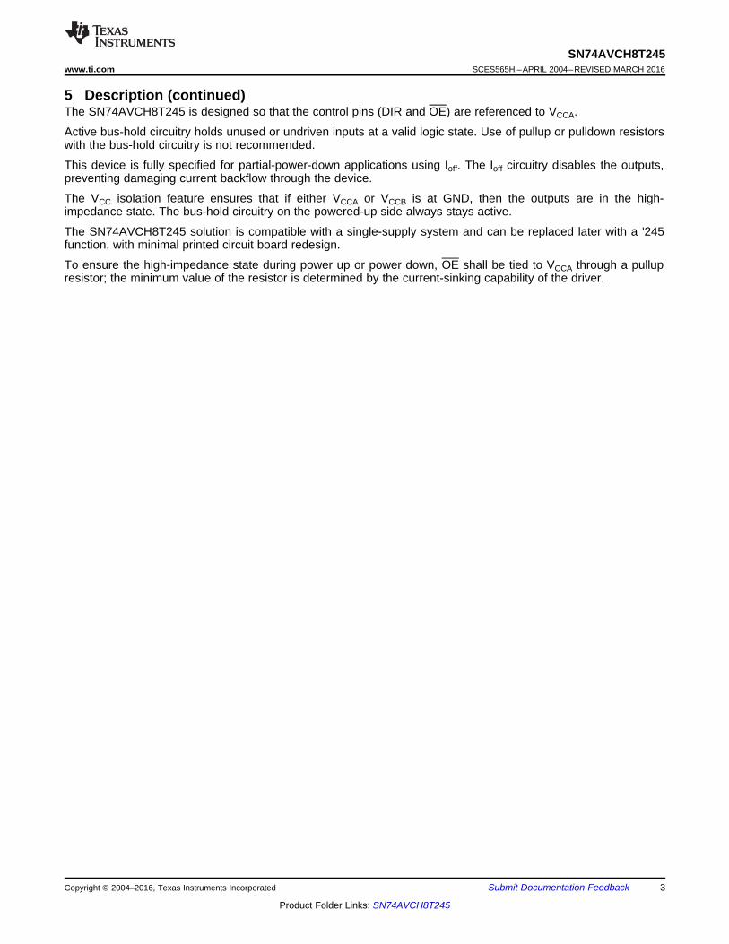
5 Description (continued)The SN74AVCH8T245 is designed so that the control pins (DIR and OE) are referenced to VCCA.
Active bus-hold circuitry holds unused or undriven inputs at a valid logic state. Use of pullup or pulldown resistorswith the bus-hold circuitry is not recommended.
This device is fully specified for partial-power-down applications using Ioff. The Ioff circuitry disables the outputs,preventing damaging current backflow through the device.
The VCC isolation feature ensures that if either VCCA or VCCB is at GND, then the outputs are in the high-impedance state. The bus-hold circuitry on the powered-up side always stays active.
The SN74AVCH8T245 solution is compatible with a single-supply system and can be replaced later with a '245function, with minimal printed circuit board redesign.
To ensure the high-impedance state during power up or power down, OE shall be tied to VCCA through a pullupresistor; the minimum value of the resistor is determined by the current-sinking capability of the driver.
1 24
12 13
2
3
4
5
6
7
8
9
10
11
23
22
21
20
19
18
17
16
15
14
VCCB
OE
B1
B2
B3
B4
B5
B6
B7
B8
DIR
A1
A2
A3
A4
A5
A6
A7
A8
GND
GN
DV
GN
D
CC
B
VC
CA1
2
3
4
5
6
7
8
9
10
11
12
24
23
22
21
20
19
18
17
16
15
14
13
VCCA
DIR
A1
A2
A3
A4
A5
A6
A7
A8
GND
GND
VCCB
VCCB
OE
B1
B2
B3
B4
B5
B6
B7
B8
GND
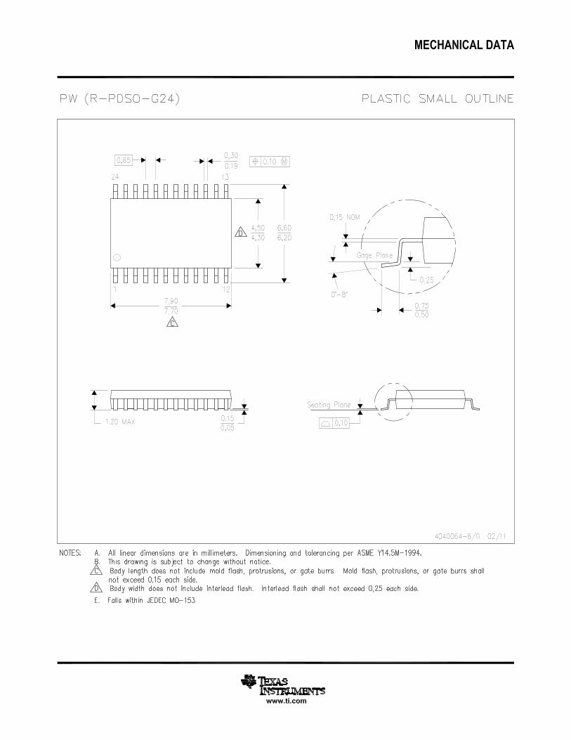
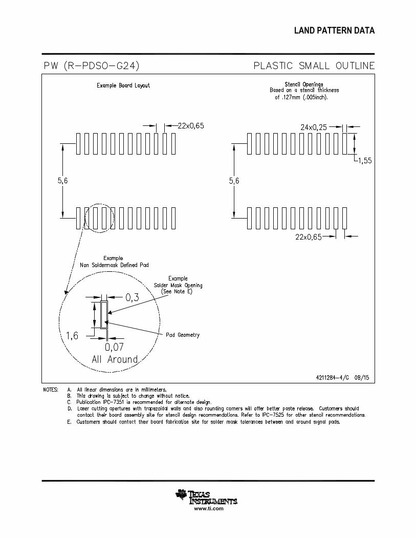
4
SN74AVCH8T245SCES565H –APRIL 2004–REVISED MARCH 2016 www.ti.com
Product Folder Links: SN74AVCH8T245
Submit Documentation Feedback Copyright © 2004–2016, Texas Instruments Incorporated
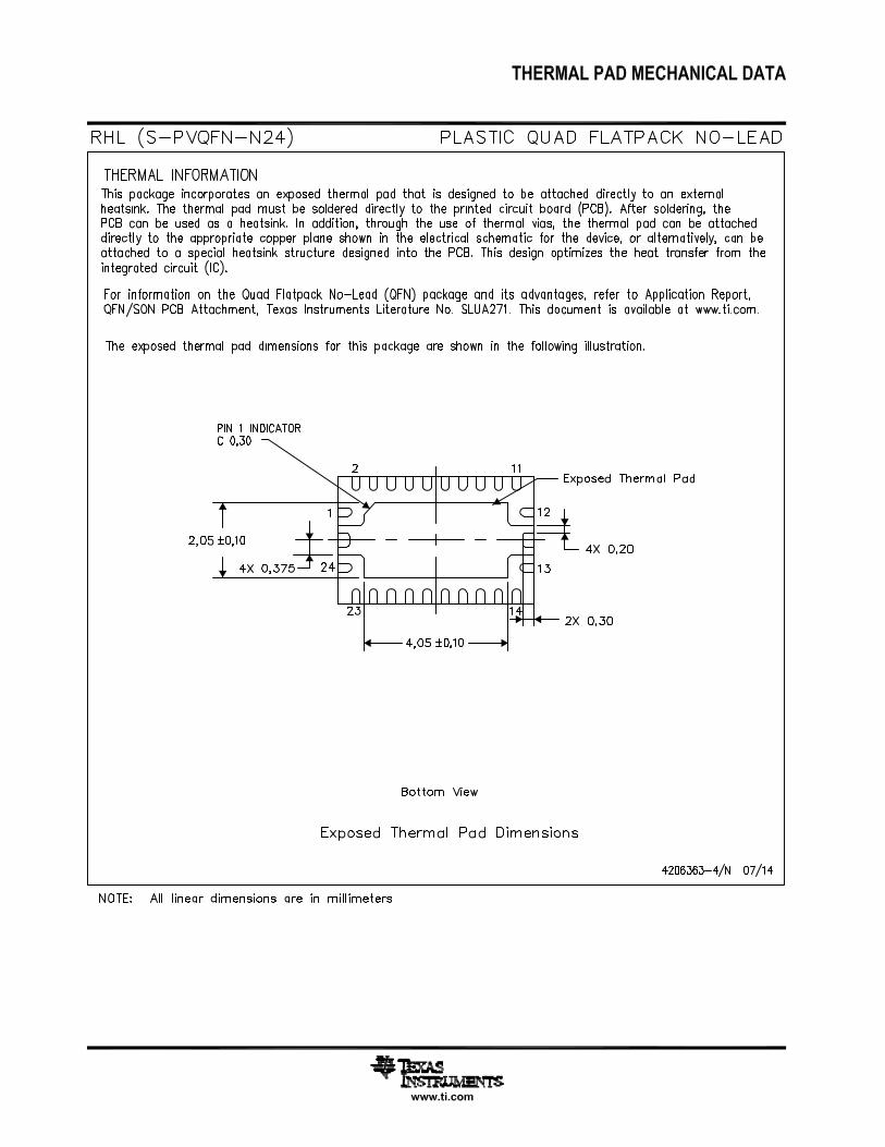
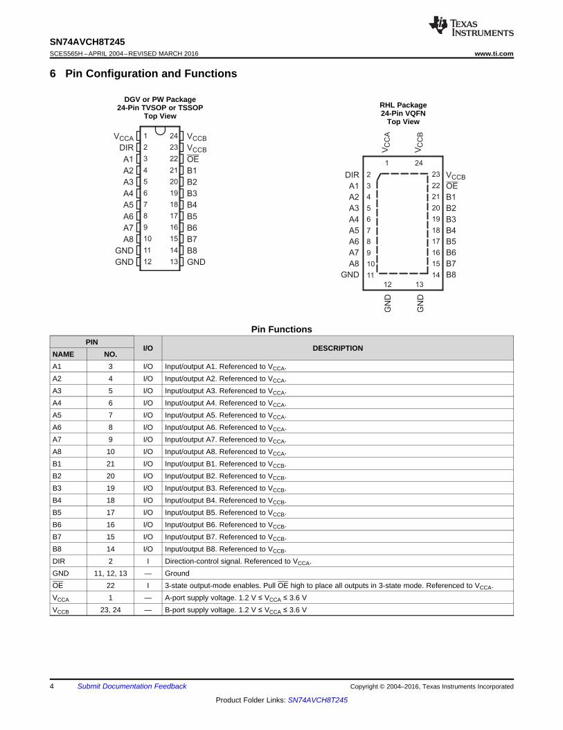
6 Pin Configuration and Functions
DGV or PW Package24-Pin TVSOP or TSSOP
Top ViewRHL Package24-Pin VQFN
Top View
Pin FunctionsPIN
I/O DESCRIPTIONNAME NO.A1 3 I/O Input/output A1. Referenced to VCCA.A2 4 I/O Input/output A2. Referenced to VCCA.A3 5 I/O Input/output A3. Referenced to VCCA.A4 6 I/O Input/output A4. Referenced to VCCA.A5 7 I/O Input/output A5. Referenced to VCCA.A6 8 I/O Input/output A6. Referenced to VCCA.A7 9 I/O Input/output A7. Referenced to VCCA.A8 10 I/O Input/output A8. Referenced to VCCA.B1 21 I/O Input/output B1. Referenced to VCCB.B2 20 I/O Input/output B2. Referenced to VCCB.B3 19 I/O Input/output B3. Referenced to VCCB.B4 18 I/O Input/output B4. Referenced to VCCB.B5 17 I/O Input/output B5. Referenced to VCCB.B6 16 I/O Input/output B6. Referenced to VCCB.B7 15 I/O Input/output B7. Referenced to VCCB.B8 14 I/O Input/output B8. Referenced to VCCB.DIR 2 I Direction-control signal. Referenced to VCCA.GND 11, 12, 13 — GroundOE 22 I 3-state output-mode enables. Pull OE high to place all outputs in 3-state mode. Referenced to VCCA.VCCA 1 — A-port supply voltage. 1.2 V ≤ VCCA ≤ 3.6 VVCCB 23, 24 — B-port supply voltage. 1.2 V ≤ VCCA ≤ 3.6 V
5
SN74AVCH8T245www.ti.com SCES565H –APRIL 2004–REVISED MARCH 2016
Product Folder Links: SN74AVCH8T245
Submit Documentation FeedbackCopyright © 2004–2016, Texas Instruments Incorporated
(1) Stresses beyond those listed under Absolute Maximum Ratings may cause permanent damage to the device. These are stress ratingsonly, which do not imply functional operation of the device at these or any other conditions beyond those indicated under RecommendedOperating Conditions. Exposure to absolute-maximum-rated conditions for extended periods may affect device reliability.
(2) The input voltage and output negative-voltage ratings may be exceeded if the input and output current ratings are observed.(3) The output positive-voltage rating may be exceeded up to 4.6 V maximum if the output current rating is observed.
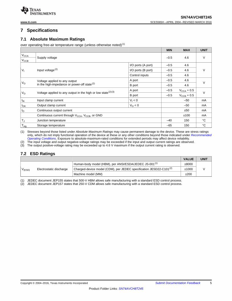
7 Specifications
7.1 Absolute Maximum Ratingsover operating free-air temperature range (unless otherwise noted) (1)
MIN MAX UNITVCCA Supply voltage –0.5 4.6 VVCCB
VI Input voltage (2)
I/O ports (A port) –0.5 4.6VI/O ports (B port) –0.5 4.6
Control inputs –0.5 4.6
VOVoltage applied to any outputin the high-impedance or power-off state (2)
A port –0.5 4.6V
B port –0.5 4.6
VO Voltage applied to any output in the high or low state (2) (3) A port –0.5 VCCA + 0.5V
B port –0.5 VCCB + 0.5IIK Input clamp current VI < 0 –50 mAIOK Output clamp current VO < 0 –50 mAIO Continuous output current ±50 mA
Continuous current through VCCA, VCCB, or GND ±100 mATJ Junction temperature –40 150 °CTstg Storage temperature –65 150 °C
(1) JEDEC document JEP155 states that 500-V HBM allows safe manufacturing with a standard ESD control process.(2) JEDEC document JEP157 states that 250-V CDM allows safe manufacturing with a standard ESD control process.
7.2 ESD RatingsVALUE UNIT
V(ESD) Electrostatic dischargeHuman-body model (HBM), per ANSI/ESDA/JEDEC JS-001 (1) ±8000
VCharged-device model (CDM), per JEDEC specification JESD22-C101 (2) ±1000Machine model (MM) ±200
6
SN74AVCH8T245SCES565H –APRIL 2004–REVISED MARCH 2016 www.ti.com
Product Folder Links: SN74AVCH8T245
Submit Documentation Feedback Copyright © 2004–2016, Texas Instruments Incorporated
(1) VCCI is the VCC associated with the input port.(2) VCCO is the VCC associated with the output port.
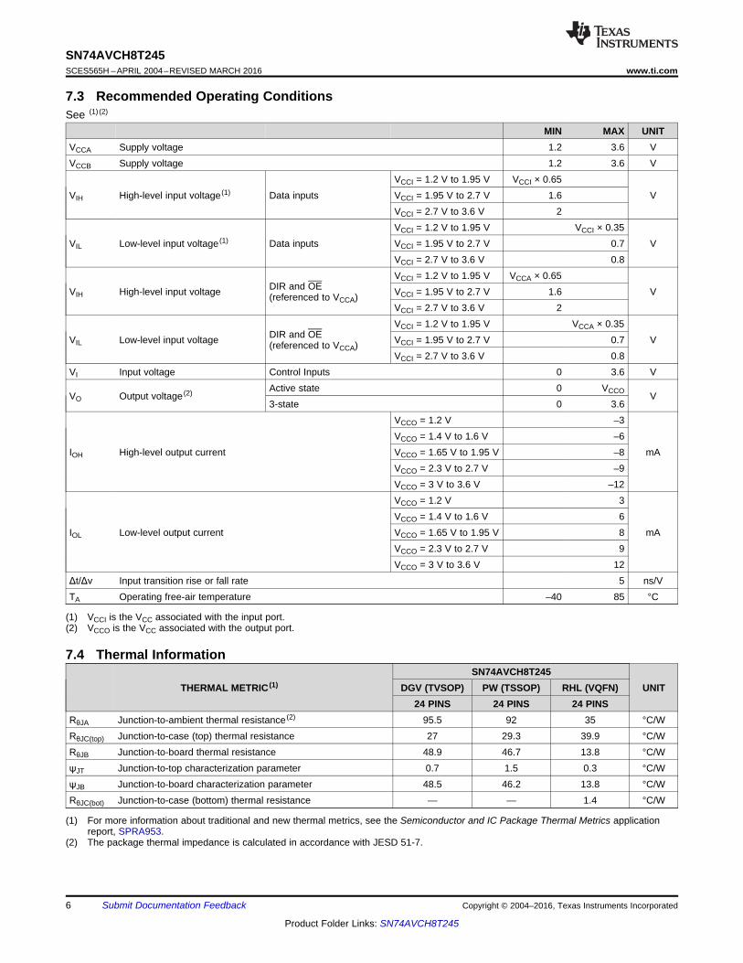
7.3 Recommended Operating ConditionsSee (1) (2)
MIN MAX UNITVCCA Supply voltage 1.2 3.6 VVCCB Supply voltage 1.2 3.6 V
VIH High-level input voltage (1) Data inputsVCCI = 1.2 V to 1.95 V VCCI × 0.65
VVCCI = 1.95 V to 2.7 V 1.6VCCI = 2.7 V to 3.6 V 2
VIL Low-level input voltage (1) Data inputsVCCI = 1.2 V to 1.95 V VCCI × 0.35
VVCCI = 1.95 V to 2.7 V 0.7VCCI = 2.7 V to 3.6 V 0.8
VIH High-level input voltage DIR and OE(referenced to VCCA)
VCCI = 1.2 V to 1.95 V VCCA × 0.65VVCCI = 1.95 V to 2.7 V 1.6
VCCI = 2.7 V to 3.6 V 2
VIL Low-level input voltage DIR and OE(referenced to VCCA)
VCCI = 1.2 V to 1.95 V VCCA × 0.35VVCCI = 1.95 V to 2.7 V 0.7
VCCI = 2.7 V to 3.6 V 0.8VI Input voltage Control Inputs 0 3.6 V
VO Output voltage (2) Active state 0 VCCO V3-state 0 3.6
IOH High-level output current
VCCO = 1.2 V –3
mAVCCO = 1.4 V to 1.6 V –6VCCO = 1.65 V to 1.95 V –8VCCO = 2.3 V to 2.7 V –9VCCO = 3 V to 3.6 V –12
IOL Low-level output current
VCCO = 1.2 V 3
mAVCCO = 1.4 V to 1.6 V 6VCCO = 1.65 V to 1.95 V 8VCCO = 2.3 V to 2.7 V 9VCCO = 3 V to 3.6 V 12
Δt/Δv Input transition rise or fall rate 5 ns/VTA Operating free-air temperature –40 85 °C
(1) For more information about traditional and new thermal metrics, see the Semiconductor and IC Package Thermal Metrics applicationreport, SPRA953.
(2) The package thermal impedance is calculated in accordance with JESD 51-7.
7.4 Thermal Information
THERMAL METRIC (1)SN74AVCH8T245
UNITDGV (TVSOP) PW (TSSOP) RHL (VQFN)24 PINS 24 PINS 24 PINS
RθJA Junction-to-ambient thermal resistance (2) 95.5 92 35 °C/WRθJC(top) Junction-to-case (top) thermal resistance 27 29.3 39.9 °C/WRθJB Junction-to-board thermal resistance 48.9 46.7 13.8 °C/WψJT Junction-to-top characterization parameter 0.7 1.5 0.3 °C/WψJB Junction-to-board characterization parameter 48.5 46.2 13.8 °C/WRθJC(bot) Junction-to-case (bottom) thermal resistance — — 1.4 °C/W
7
SN74AVCH8T245www.ti.com SCES565H –APRIL 2004–REVISED MARCH 2016
Product Folder Links: SN74AVCH8T245
Submit Documentation FeedbackCopyright © 2004–2016, Texas Instruments Incorporated
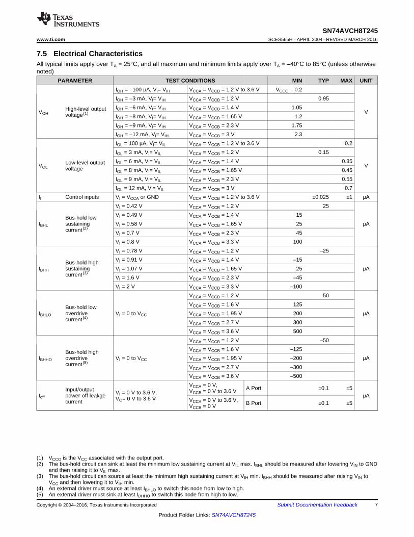
(1) VCCO is the VCC associated with the output port.(2) The bus-hold circuit can sink at least the minimum low sustaining current at VIL max. IBHL should be measured after lowering VIN to GND
and then raising it to VIL max.(3) The bus-hold circuit can source at least the minimum high sustaining current at VIH min. IBHH should be measured after raising VIN to
VCC and then lowering it to VIH min.(4) An external driver must source at least IBHLO to switch this node from low to high.(5) An external driver must sink at least IBHHO to switch this node from high to low.
7.5 Electrical CharacteristicsAll typical limits apply over TA = 25°C, and all maximum and minimum limits apply over TA = –40°C to 85°C (unless otherwisenoted)
PARAMETER TEST CONDITIONS MIN TYP MAX UNIT
VOHHigh-level outputvoltage (1)
IOH = –100 μA, VI= VIH VCCA = VCCB = 1.2 V to 3.6 V VCCO – 0.2
V
IOH = –3 mA, VI= VIH VCCA = VCCB = 1.2 V 0.95IOH = –6 mA, VI= VIH VCCA = VCCB = 1.4 V 1.05IOH = –8 mA, VI= VIH VCCA = VCCB = 1.65 V 1.2IOH = –9 mA, VI= VIH VCCA = VCCB = 2.3 V 1.75IOH = –12 mA, VI= VIH VCCA = VCCB = 3 V 2.3
VOLLow-level outputvoltage
IOL = 100 µA, VI= VIL VCCA = VCCB = 1.2 V to 3.6 V 0.2
V
IOL = 3 mA, VI= VIL VCCA = VCCB = 1.2 V 0.15IOL = 6 mA, VI= VIL VCCA = VCCB = 1.4 V 0.35IOL = 8 mA, VI= VIL VCCA = VCCB = 1.65 V 0.45IOL = 9 mA, VI= VIL VCCA = VCCB = 2.3 V 0.55IOL = 12 mA, VI= VIL VCCA = VCCB = 3 V 0.7
II Control inputs VI = VCCA or GND VCCA = VCCB = 1.2 V to 3.6 V ±0.025 ±1 μA
IBHL
Bus-hold lowsustainingcurrent (2)
VI = 0.42 V VCCA = VCCB = 1.2 V 25
μAVI = 0.49 V VCCA = VCCB = 1.4 V 15VI = 0.58 V VCCA = VCCB = 1.65 V 25VI = 0.7 V VCCA = VCCB = 2.3 V 45VI = 0.8 V VCCA = VCCB = 3.3 V 100
IBHH
Bus-hold highsustainingcurrent (3)
VI = 0.78 V VCCA = VCCB = 1.2 V –25
μAVI = 0.91 V VCCA = VCCB = 1.4 V –15VI = 1.07 V VCCA = VCCB = 1.65 V –25VI = 1.6 V VCCA = VCCB = 2.3 V –45VI = 2 V VCCA = VCCB = 3.3 V –100
IBHLO
Bus-hold lowoverdrivecurrent (4)
VI = 0 to VCC
VCCA = VCCB = 1.2 V 50
μAVCCA = VCCB = 1.6 V 125VCCA = VCCB = 1.95 V 200VCCA = VCCB = 2.7 V 300VCCA = VCCB = 3.6 V 500
IBHHO
Bus-hold highoverdrivecurrent (5)
VI = 0 to VCC
VCCA = VCCB = 1.2 V –50
μAVCCA = VCCB = 1.6 V –125VCCA = VCCB = 1.95 V –200VCCA = VCCB = 2.7 V –300VCCA = VCCB = 3.6 V –500
Ioff
Input/outputpower-off leakgecurrent
VI = 0 V to 3.6 V,VO= 0 V to 3.6 V
VCCA = 0 V,VCCB = 0 V to 3.6 V A Port ±0.1 ±5
μAVCCA = 0 V to 3.6 V,VCCB = 0 V B Port ±0.1 ±5
8
SN74AVCH8T245SCES565H –APRIL 2004–REVISED MARCH 2016 www.ti.com
Product Folder Links: SN74AVCH8T245
Submit Documentation Feedback Copyright © 2004–2016, Texas Instruments Incorporated
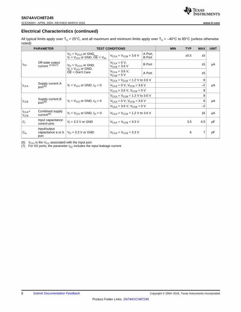
Electrical Characteristics (continued)All typical limits apply over TA = 25°C, and all maximum and minimum limits apply over TA = –40°C to 85°C (unless otherwisenoted)
PARAMETER TEST CONDITIONS MIN TYP MAX UNIT
(6) VCCI is the VCC associated with the input port.(7) For I/O ports, the parameter IOZ includes the input leakage current.
IOZOff-state outputcurrent (1) (6) (7)
VO = VCCO or GND,VI = VCCI or GND, OE = VIH
VCCA = VCCB = 3.6 V A Port,B Port ±0.5 ±5
μAVO = VCCO or GND,VI = VCCI or GND,OE = Don't Care
VCCA = 0 V,VCCB = 3.6 V B Port ±5
VCCA = 3.6 V,VCCB = 0 V A Port ±5
ICCASupply current Aport (6) VI = VCCI or GND, IO = 0
VCCA = VCCB = 1.2 V to 3.6 V 8μAVCCA = 0 V, VCCB = 3.6 V –2
VCCA = 3.6 V, VCCB = 0 V 8
ICCBSupply current Bport (6) VI = VCCI or GND, IO = 0
VCCA = VCCB = 1.2 V to 3.6 V 8μAVCCA = 0 V, VCCB = 3.6 V 8
VCCA = 3.6 V, VCCB = 0 V –2ICCA+ICCB
Combined supplycurrent (6) VI = VCCI or GND, IO = 0 VCCA = VCCB = 1.2 V to 3.6 V 16 μA
CiInput capacitancecontrol pins VI = 3.3 V or GND VCCA = VCCB = 3.3 V 3.5 4.5 pF
Cio
Input/outputcapacitance a or bport
VO = 3.3 V or GND VCCA = VCCB = 3.3 V 6 7 pF
9
SN74AVCH8T245www.ti.com SCES565H –APRIL 2004–REVISED MARCH 2016
Product Folder Links: SN74AVCH8T245
Submit Documentation FeedbackCopyright © 2004–2016, Texas Instruments Incorporated
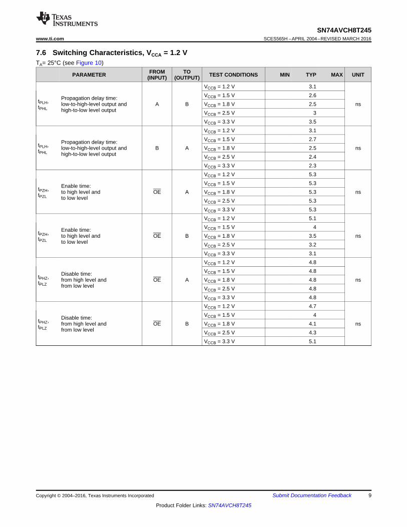
7.6 Switching Characteristics, VCCA = 1.2 VTA= 25°C (see Figure 10)
PARAMETER FROM(INPUT)
TO(OUTPUT) TEST CONDITIONS MIN TYP MAX UNIT
tPLH,tPHL
Propagation delay time:low-to-high-level output andhigh-to-low level output
A B
VCCB = 1.2 V 3.1
nsVCCB = 1.5 V 2.6VCCB = 1.8 V 2.5VCCB = 2.5 V 3VCCB = 3.3 V 3.5
tPLH,tPHL
Propagation delay time:low-to-high-level output andhigh-to-low level output
B A
VCCB = 1.2 V 3.1
nsVCCB = 1.5 V 2.7VCCB = 1.8 V 2.5VCCB = 2.5 V 2.4VCCB = 3.3 V 2.3
tPZH,tPZL
Enable time:to high level andto low level
OE A
VCCB = 1.2 V 5.3
nsVCCB = 1.5 V 5.3VCCB = 1.8 V 5.3VCCB = 2.5 V 5.3VCCB = 3.3 V 5.3
tPZH,tPZL
Enable time:to high level andto low level
OE B
VCCB = 1.2 V 5.1
nsVCCB = 1.5 V 4VCCB = 1.8 V 3.5VCCB = 2.5 V 3.2VCCB = 3.3 V 3.1
tPHZ,tPLZ
Disable time:from high level andfrom low level
OE A
VCCB = 1.2 V 4.8
nsVCCB = 1.5 V 4.8VCCB = 1.8 V 4.8VCCB = 2.5 V 4.8VCCB = 3.3 V 4.8
tPHZ,tPLZ
Disable time:from high level andfrom low level
OE B
VCCB = 1.2 V 4.7
nsVCCB = 1.5 V 4VCCB = 1.8 V 4.1VCCB = 2.5 V 4.3VCCB = 3.3 V 5.1
10
SN74AVCH8T245SCES565H –APRIL 2004–REVISED MARCH 2016 www.ti.com
Product Folder Links: SN74AVCH8T245
Submit Documentation Feedback Copyright © 2004–2016, Texas Instruments Incorporated
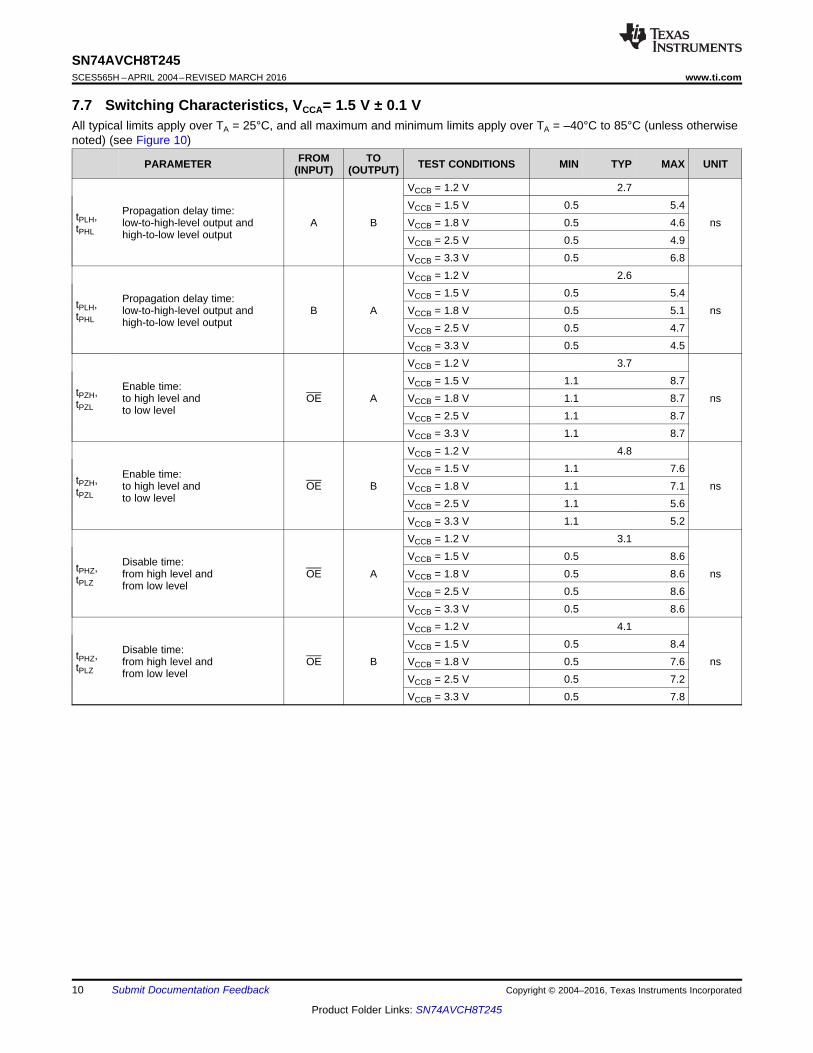
7.7 Switching Characteristics, VCCA= 1.5 V ± 0.1 VAll typical limits apply over TA = 25°C, and all maximum and minimum limits apply over TA = –40°C to 85°C (unless otherwisenoted) (see Figure 10)
PARAMETER FROM(INPUT)
TO(OUTPUT) TEST CONDITIONS MIN TYP MAX UNIT
tPLH,tPHL
Propagation delay time:low-to-high-level output andhigh-to-low level output
A B
VCCB = 1.2 V 2.7
nsVCCB = 1.5 V 0.5 5.4VCCB = 1.8 V 0.5 4.6VCCB = 2.5 V 0.5 4.9VCCB = 3.3 V 0.5 6.8
tPLH,tPHL
Propagation delay time:low-to-high-level output andhigh-to-low level output
B A
VCCB = 1.2 V 2.6
nsVCCB = 1.5 V 0.5 5.4VCCB = 1.8 V 0.5 5.1VCCB = 2.5 V 0.5 4.7VCCB = 3.3 V 0.5 4.5
tPZH,tPZL
Enable time:to high level andto low level
OE A
VCCB = 1.2 V 3.7
nsVCCB = 1.5 V 1.1 8.7VCCB = 1.8 V 1.1 8.7VCCB = 2.5 V 1.1 8.7VCCB = 3.3 V 1.1 8.7
tPZH,tPZL
Enable time:to high level andto low level
OE B
VCCB = 1.2 V 4.8
nsVCCB = 1.5 V 1.1 7.6VCCB = 1.8 V 1.1 7.1VCCB = 2.5 V 1.1 5.6VCCB = 3.3 V 1.1 5.2
tPHZ,tPLZ
Disable time:from high level andfrom low level
OE A
VCCB = 1.2 V 3.1
nsVCCB = 1.5 V 0.5 8.6VCCB = 1.8 V 0.5 8.6VCCB = 2.5 V 0.5 8.6VCCB = 3.3 V 0.5 8.6
tPHZ,tPLZ
Disable time:from high level andfrom low level
OE B
VCCB = 1.2 V 4.1
nsVCCB = 1.5 V 0.5 8.4VCCB = 1.8 V 0.5 7.6VCCB = 2.5 V 0.5 7.2VCCB = 3.3 V 0.5 7.8
11
SN74AVCH8T245www.ti.com SCES565H –APRIL 2004–REVISED MARCH 2016
Product Folder Links: SN74AVCH8T245
Submit Documentation FeedbackCopyright © 2004–2016, Texas Instruments Incorporated
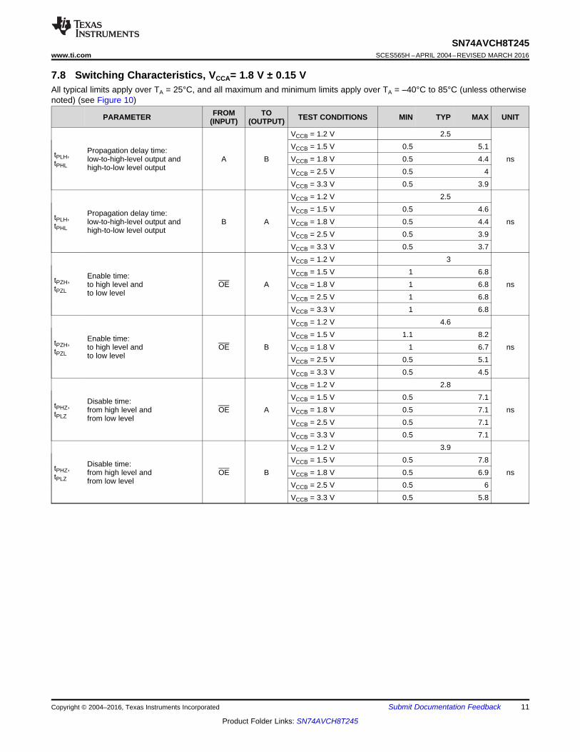
7.8 Switching Characteristics, VCCA= 1.8 V ± 0.15 VAll typical limits apply over TA = 25°C, and all maximum and minimum limits apply over TA = –40°C to 85°C (unless otherwisenoted) (see Figure 10)
PARAMETER FROM(INPUT)
TO(OUTPUT) TEST CONDITIONS MIN TYP MAX UNIT
tPLH,tPHL
Propagation delay time:low-to-high-level output andhigh-to-low level output
A B
VCCB = 1.2 V 2.5
nsVCCB = 1.5 V 0.5 5.1VCCB = 1.8 V 0.5 4.4VCCB = 2.5 V 0.5 4VCCB = 3.3 V 0.5 3.9
tPLH,tPHL
Propagation delay time:low-to-high-level output andhigh-to-low level output
B A
VCCB = 1.2 V 2.5
nsVCCB = 1.5 V 0.5 4.6VCCB = 1.8 V 0.5 4.4VCCB = 2.5 V 0.5 3.9VCCB = 3.3 V 0.5 3.7
tPZH,tPZL
Enable time:to high level andto low level
OE A
VCCB = 1.2 V 3
nsVCCB = 1.5 V 1 6.8VCCB = 1.8 V 1 6.8VCCB = 2.5 V 1 6.8VCCB = 3.3 V 1 6.8
tPZH,tPZL
Enable time:to high level andto low level
OE B
VCCB = 1.2 V 4.6
nsVCCB = 1.5 V 1.1 8.2VCCB = 1.8 V 1 6.7VCCB = 2.5 V 0.5 5.1VCCB = 3.3 V 0.5 4.5
tPHZ,tPLZ
Disable time:from high level andfrom low level
OE A
VCCB = 1.2 V 2.8
nsVCCB = 1.5 V 0.5 7.1VCCB = 1.8 V 0.5 7.1VCCB = 2.5 V 0.5 7.1VCCB = 3.3 V 0.5 7.1
tPHZ,tPLZ
Disable time:from high level andfrom low level
OE B
VCCB = 1.2 V 3.9
nsVCCB = 1.5 V 0.5 7.8VCCB = 1.8 V 0.5 6.9VCCB = 2.5 V 0.5 6VCCB = 3.3 V 0.5 5.8
12
SN74AVCH8T245SCES565H –APRIL 2004–REVISED MARCH 2016 www.ti.com
Product Folder Links: SN74AVCH8T245
Submit Documentation Feedback Copyright © 2004–2016, Texas Instruments Incorporated
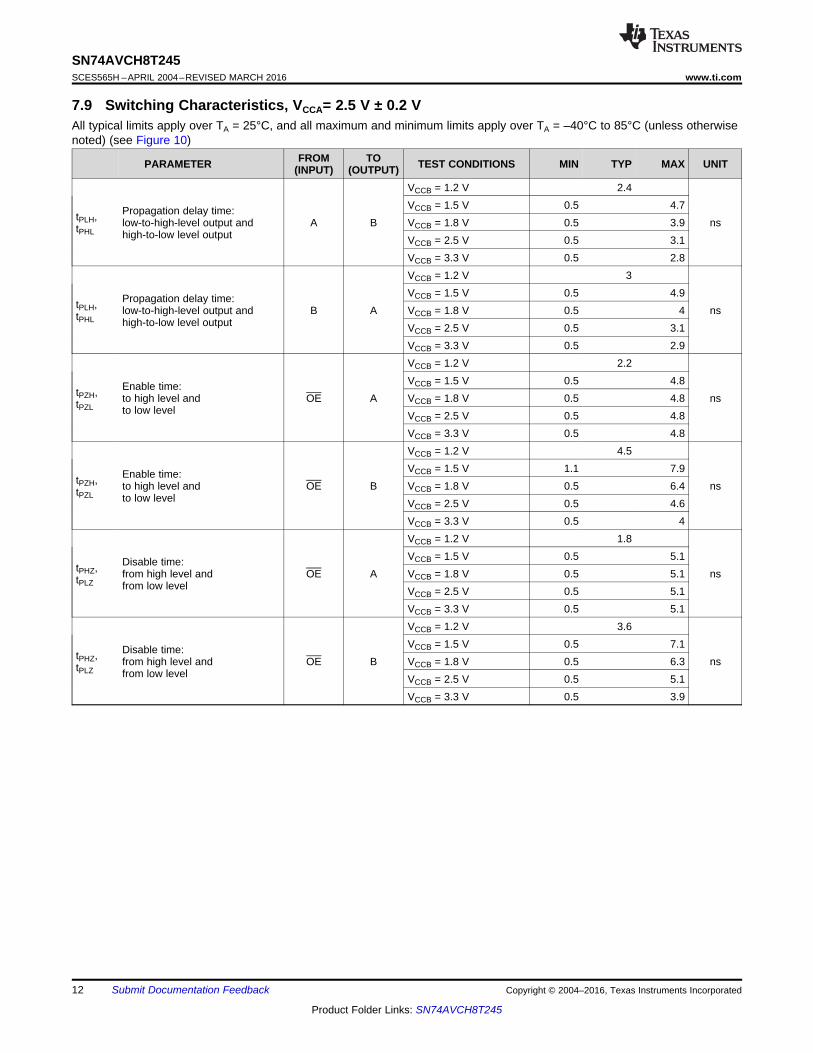
7.9 Switching Characteristics, VCCA= 2.5 V ± 0.2 VAll typical limits apply over TA = 25°C, and all maximum and minimum limits apply over TA = –40°C to 85°C (unless otherwisenoted) (see Figure 10)
PARAMETER FROM(INPUT)
TO(OUTPUT) TEST CONDITIONS MIN TYP MAX UNIT
tPLH,tPHL
Propagation delay time:low-to-high-level output andhigh-to-low level output
A B
VCCB = 1.2 V 2.4
nsVCCB = 1.5 V 0.5 4.7VCCB = 1.8 V 0.5 3.9VCCB = 2.5 V 0.5 3.1VCCB = 3.3 V 0.5 2.8
tPLH,tPHL
Propagation delay time:low-to-high-level output andhigh-to-low level output
B A
VCCB = 1.2 V 3
nsVCCB = 1.5 V 0.5 4.9VCCB = 1.8 V 0.5 4VCCB = 2.5 V 0.5 3.1VCCB = 3.3 V 0.5 2.9
tPZH,tPZL
Enable time:to high level andto low level
OE A
VCCB = 1.2 V 2.2
nsVCCB = 1.5 V 0.5 4.8VCCB = 1.8 V 0.5 4.8VCCB = 2.5 V 0.5 4.8VCCB = 3.3 V 0.5 4.8
tPZH,tPZL
Enable time:to high level andto low level
OE B
VCCB = 1.2 V 4.5
nsVCCB = 1.5 V 1.1 7.9VCCB = 1.8 V 0.5 6.4VCCB = 2.5 V 0.5 4.6VCCB = 3.3 V 0.5 4
tPHZ,tPLZ
Disable time:from high level andfrom low level
OE A
VCCB = 1.2 V 1.8
nsVCCB = 1.5 V 0.5 5.1VCCB = 1.8 V 0.5 5.1VCCB = 2.5 V 0.5 5.1VCCB = 3.3 V 0.5 5.1
tPHZ,tPLZ
Disable time:from high level andfrom low level
OE B
VCCB = 1.2 V 3.6
nsVCCB = 1.5 V 0.5 7.1VCCB = 1.8 V 0.5 6.3VCCB = 2.5 V 0.5 5.1VCCB = 3.3 V 0.5 3.9
13
SN74AVCH8T245www.ti.com SCES565H –APRIL 2004–REVISED MARCH 2016
Product Folder Links: SN74AVCH8T245
Submit Documentation FeedbackCopyright © 2004–2016, Texas Instruments Incorporated
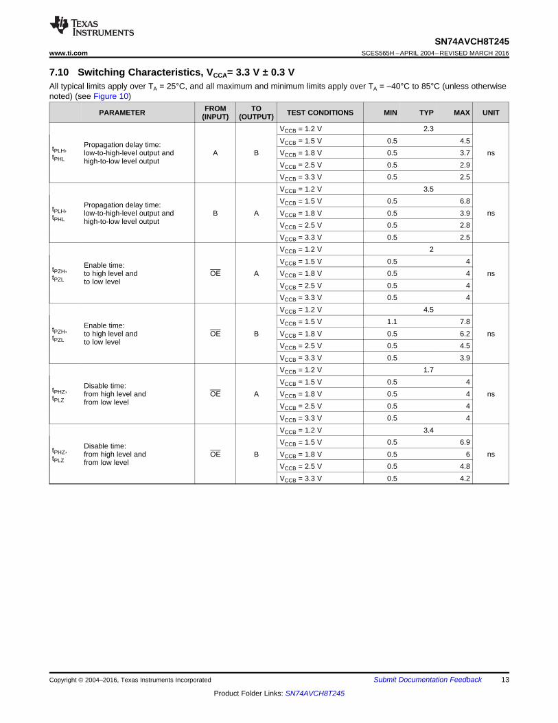
7.10 Switching Characteristics, VCCA= 3.3 V ± 0.3 VAll typical limits apply over TA = 25°C, and all maximum and minimum limits apply over TA = –40°C to 85°C (unless otherwisenoted) (see Figure 10)
PARAMETER FROM(INPUT)
TO(OUTPUT) TEST CONDITIONS MIN TYP MAX UNIT
tPLH,tPHL
Propagation delay time:low-to-high-level output andhigh-to-low level output
A B
VCCB = 1.2 V 2.3
nsVCCB = 1.5 V 0.5 4.5VCCB = 1.8 V 0.5 3.7VCCB = 2.5 V 0.5 2.9VCCB = 3.3 V 0.5 2.5
tPLH,tPHL
Propagation delay time:low-to-high-level output andhigh-to-low level output
B A
VCCB = 1.2 V 3.5
nsVCCB = 1.5 V 0.5 6.8VCCB = 1.8 V 0.5 3.9VCCB = 2.5 V 0.5 2.8VCCB = 3.3 V 0.5 2.5
tPZH,tPZL
Enable time:to high level andto low level
OE A
VCCB = 1.2 V 2
nsVCCB = 1.5 V 0.5 4VCCB = 1.8 V 0.5 4VCCB = 2.5 V 0.5 4VCCB = 3.3 V 0.5 4
tPZH,tPZL
Enable time:to high level andto low level
OE B
VCCB = 1.2 V 4.5
nsVCCB = 1.5 V 1.1 7.8VCCB = 1.8 V 0.5 6.2VCCB = 2.5 V 0.5 4.5VCCB = 3.3 V 0.5 3.9
tPHZ,tPLZ
Disable time:from high level andfrom low level
OE A
VCCB = 1.2 V 1.7
nsVCCB = 1.5 V 0.5 4VCCB = 1.8 V 0.5 4VCCB = 2.5 V 0.5 4VCCB = 3.3 V 0.5 4
tPHZ,tPLZ
Disable time:from high level andfrom low level
OE B
VCCB = 1.2 V 3.4
nsVCCB = 1.5 V 0.5 6.9VCCB = 1.8 V 0.5 6VCCB = 2.5 V 0.5 4.8VCCB = 3.3 V 0.5 4.2
14
SN74AVCH8T245SCES565H –APRIL 2004–REVISED MARCH 2016 www.ti.com
Product Folder Links: SN74AVCH8T245
Submit Documentation Feedback Copyright © 2004–2016, Texas Instruments Incorporated
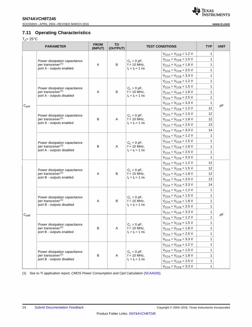
(1) See to TI application report, CMOS Power Consumption and Cpd Calculation (SCAA035).
7.11 Operating CharacteristicsTA= 25°C
PARAMETER FROM(INPUT)
TO(OUTPUT) TEST CONDITIONS TYP UNIT
CpdA
Power dissipation capacitanceper transceiver (1)
port A - outputs enabledA B
CL = 0 pF,f = 10 MHz,tr = tf = 1 ns
VCCA = VCCB = 1.2 V 1
pF
VCCA = VCCB = 1.5 V 1VCCA = VCCB = 1.8 V 1VCCA = VCCB = 2.5 V 1VCCA = VCCB = 3.3 V 1
Power dissipation capacitanceper transceiver (1)
port A - outputs disabledA B
CL = 0 pF,f = 10 MHz,tr = tf = 1 ns
VCCA = VCCB = 1.2 V 1VCCA = VCCB = 1.5 V 1VCCA = VCCB = 1.8 V 1VCCA = VCCB = 2.5 V 1VCCA = VCCB = 3.3 V 1
Power dissipation capacitanceper transceiver (1)
port A - outputs enabledB A
CL = 0 pF,f = 10 MHz,tr = tf = 1 ns
VCCA = VCCB = 1.2 V 12VCCA = VCCB = 1.5 V 12VCCA = VCCB = 1.8 V 12VCCA = VCCB = 2.5 V 13VCCA = VCCB = 3.3 V 14
Power dissipation capacitanceper transceiver (1)
port A - outputs disabledB A
CL = 0 pF,f = 10 MHz,tr = tf = 1 ns
VCCA = VCCB = 1.2 V 1VCCA = VCCB = 1.5 V 1VCCA = VCCB = 1.8 V 1VCCA = VCCB = 2.5 V 1VCCA = VCCB = 3.3 V 1
CpdB
Power dissipation capacitanceper transceiver (1)
port B - outputs enabledA B
CL = 0 pF,f = 10 MHz,tr = tf = 1 ns
VCCA = VCCB = 1.2 V 12
pF
VCCA = VCCB = 1.5 V 12VCCA = VCCB = 1.8 V 12VCCA = VCCB = 2.5 V 13VCCA = VCCB = 3.3 V 14
Power dissipation capacitanceper transceiver (1)
port B - outputs disabledA B
CL = 0 pF,f = 10 MHz,tr = tf = 1 ns
VCCA = VCCB = 1.2 V 1VCCA = VCCB = 1.5 V 1VCCA = VCCB = 1.8 V 1VCCA = VCCB = 2.5 V 1VCCA = VCCB = 3.3 V 1
Power dissipation capacitanceper transceiver (1)
port B - outputs enabledB A
CL = 0 pF,f = 10 MHz,tr = tf = 1 ns
VCCA = VCCB = 1.2 V 1VCCA = VCCB = 1.5 V 1VCCA = VCCB = 1.8 V 1VCCA = VCCB = 2.5 V 1VCCA = VCCB = 3.3 V 1
Power dissipation capacitanceper transceiver (1)
port B - outputs disabledB A
CL = 0 pF,f = 10 MHz,tr = tf = 1 ns
VCCA = VCCB = 1.2 V 1VCCA = VCCB = 1.5 V 1VCCA = VCCB = 1.8 V 1VCCA = VCCB = 2.5 V 1VCCA = VCCB = 3.3 V 1
0
1
2
3
4
5
6
0 10 20 30 40 50 60
VCCB = 1.8 V
VCCB = 2.5 V
VCCB = 3.3 V
VCCB = 1.5 V
VCCB = 1.2 V
t PH
L−
ns
CL − pF CL − pF
t PL
H−
ns
VCCB = 1.8 V
VCCB = 2.5 V
VCCB = 3.3 V
VCCB = 1.5 V
VCCB = 1.2 V
0
1
2
3
4
5
6
0 10 20 30 40 50 60
0
1
2
3
4
5
6
0 10 20 30 40 50 60
t PH
L−
ns
CL − pF
VCCB = 1.8 V
VCCB = 2.5 V
VCCB = 3.3 V
VCCB = 1.5 V
VCCB = 1.2 V
CL − pF
t PL
H−
ns
0 10 20 30 40 50 600
1
2
3
4
5
6
VCCB = 1.8 V
VCCB = 2.5 V
VCCB = 3.3 V
VCCB = 1.5 V
VCCB = 1.2 V
0
1
2
3
4
5
6
0 10 20 30 40 50
t PD
−n
s
CL − pF
60
VCCB = 1.8 V
VCCB = 2.5 V
VCCB = 3.3 V
VCCB = 1.5 V
VCCB = 1.2 V
CL − pF
0
1
2
3
4
5
6
VCCB = 1.8 V
VCCB = 2.5 V
VCCB = 3.3 V
VCCB = 1.5 V
VCCB = 1.2 V
0 10 20 30 40 50 60
t PL
H−
ns
15
SN74AVCH8T245www.ti.com SCES565H –APRIL 2004–REVISED MARCH 2016
Product Folder Links: SN74AVCH8T245
Submit Documentation FeedbackCopyright © 2004–2016, Texas Instruments Incorporated
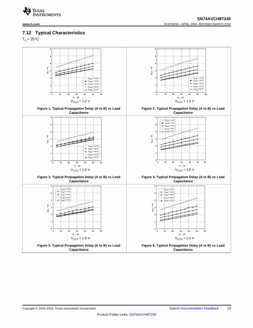
7.12 Typical CharacteristicsTA = 25°C
VCCA = 1.2 V
Figure 1. Typical Propagation Delay (A to B) vs LoadCapacitance
VCCA = 1.5 V
Figure 2. Typical Propagation Delay (A to B) vs LoadCapacitance
VCCA = 1.5 V
Figure 3. Typical Propagation Delay (A to B) vs LoadCapacitance
VCCA = 1.8 V
Figure 4. Typical Propagation Delay (A to B) vs LoadCapacitance
VCCA = 1.8 V
Figure 5. Typical Propagation Delay (A to B) vs LoadCapacitance
VCCA = 2.5 V
Figure 6. Typical Propagation Delay (A to B) vs LoadCapacitance
0
1
2
3
4
5
6
0 10 20 30 40 50 60
VCCB = 1.8 V
VCCB = 2.5 V
VCCB = 3.3 V
VCCB = 1.5 V
VCCB = 1.2 V
CL − pF
t PH
L−
ns
0
1
2
3
4
5
6
0 10 20 30 40 50 60
VCCB = 1.8 V
VCCB = 2.5 V
VCCB = 3.3 V
VCCB = 1.5 V
VCCB = 1.2 V
CL − pF
t PH
L−
ns
t PL
H−
ns
0
1
2
3
4
5
6
VCCB = 1.8 V
VCCB = 2.5 V
VCCB = 3.3 V
VCCB = 1.5 V
VCCB = 1.2 V
CL − pF
0 10 20 30 40 50 60
16
SN74AVCH8T245SCES565H –APRIL 2004–REVISED MARCH 2016 www.ti.com
Product Folder Links: SN74AVCH8T245
Submit Documentation Feedback Copyright © 2004–2016, Texas Instruments Incorporated
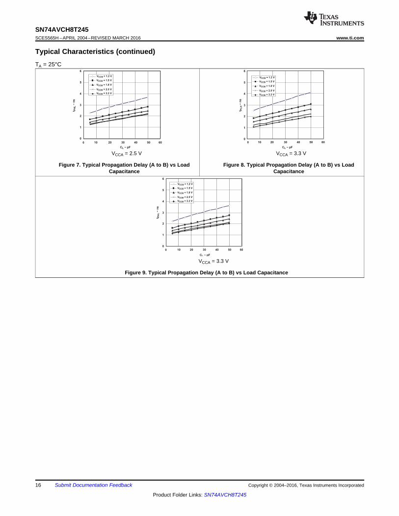
Typical Characteristics (continued)TA = 25°C
VCCA = 2.5 V
Figure 7. Typical Propagation Delay (A to B) vs LoadCapacitance
VCCA = 3.3 V
Figure 8. Typical Propagation Delay (A to B) vs LoadCapacitance
VCCA = 3.3 V
Figure 9. Typical Propagation Delay (A to B) vs Load Capacitance
VOH
VOL
From Output
Under Test
CL
(see Note A)
LOAD CIRCUIT
S1
2 × VCCO
Open
GND
RL
RL
tPLH tPHL
Output
Control
(low-level
enabling)
Output
Waveform 1
S1 at 2 × VCCO
(see Note B)Output
Waveform 2
S1 at GND
(see Note B)
tPZL
tPZH
tPLZ
tPHZ
VCCA/2VCCA/2
VCCI/2 VCCI/2
VCCI
0 V
VCCO/2 VCCO/2
VOH
VOL
0 V
VCCO/2VOL + VTP
VCCO/2VOH − VTP
0 V
VCCI
0 V
VCCI/2 VCCI/2
tw
Input
VCCA
VCCO
VOLTAGE WAVEFORMS
PROPAGATION DELAY TIMES
VOLTAGE WAVEFORMS
PULSE DURATION
VOLTAGE WAVEFORMS
ENABLE AND DISABLE TIMES
Output
Input
tpd
tPLZ/tPZL
tPHZ/tPZH
Open
2 × VCCO
GND
TEST S1
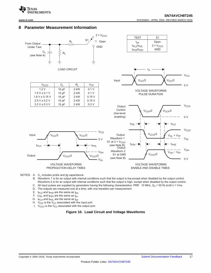
NOTES: A. CL includes probe and jig capacitance.
B. Waveform 1 is for an output with internal conditions such that the output is low, except when disabled by the output control.
Waveform 2 is for an output with internal conditions such that the output is high, except when disabled by the output control.
C. All input pulses are supplied by generators having the following characteristics: PRR 10 MHz, ZO = 50 W, dv/dt ≥ 1 V/ns.
D. The outputs are measured one at a time, with one transition per measurement.
E. tPLZ and tPHZ are the same as tdis.
F. tPZL and tPZH are the same as ten.
G. tPLH and tPHL are the same as tpd.
H. VCCI is the VCC associated with the input port.
I. VCCO is the VCC associated with the output port.
1.2 V
1.5 V ± 0.1 V
1.8 V ± 0.15 V
2.5 V ± 0.2 V
3.3 V ± 0.3 V
2 kW
2 kW
2 kW
2 kW
2 kW
VCCO RL
0.1 V
0.1 V
0.15 V
0.15 V
0.3 V
VTPCL
15 pF
15 pF
15 pF
15 pF
15 pF
17
SN74AVCH8T245www.ti.com SCES565H –APRIL 2004–REVISED MARCH 2016
Product Folder Links: SN74AVCH8T245
Submit Documentation FeedbackCopyright © 2004–2016, Texas Instruments Incorporated
8 Parameter Measurement Information
Figure 10. Load Circuit and Voltage Waveforms
DIR
OE
A1
B1
To Seven Other Channels
2
3
22
21
18
SN74AVCH8T245SCES565H –APRIL 2004–REVISED MARCH 2016 www.ti.com
Product Folder Links: SN74AVCH8T245
Submit Documentation Feedback Copyright © 2004–2016, Texas Instruments Incorporated
9 Detailed Description
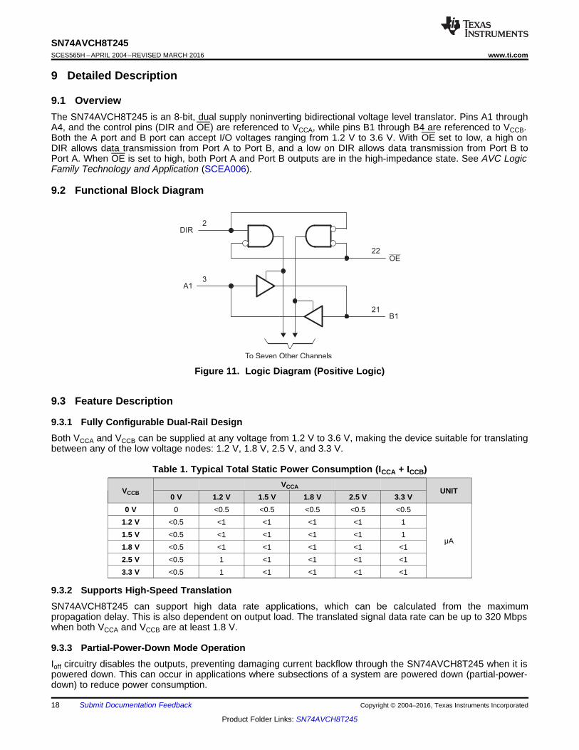
9.1 OverviewThe SN74AVCH8T245 is an 8-bit, dual supply noninverting bidirectional voltage level translator. Pins A1 throughA4, and the control pins (DIR and OE) are referenced to VCCA, while pins B1 through B4 are referenced to VCCB.Both the A port and B port can accept I/O voltages ranging from 1.2 V to 3.6 V. With OE set to low, a high onDIR allows data transmission from Port A to Port B, and a low on DIR allows data transmission from Port B toPort A. When OE is set to high, both Port A and Port B outputs are in the high-impedance state. See AVC LogicFamily Technology and Application (SCEA006).
9.2 Functional Block Diagram
Figure 11. Logic Diagram (Positive Logic)
9.3 Feature Description
9.3.1 Fully Configurable Dual-Rail DesignBoth VCCA and VCCB can be supplied at any voltage from 1.2 V to 3.6 V, making the device suitable for translatingbetween any of the low voltage nodes: 1.2 V, 1.8 V, 2.5 V, and 3.3 V.
Table 1. Typical Total Static Power Consumption (ICCA + ICCB)
VCCBVCCA UNIT
0 V 1.2 V 1.5 V 1.8 V 2.5 V 3.3 V0 V 0 <0.5 <0.5 <0.5 <0.5 <0.5
μA
1.2 V <0.5 <1 <1 <1 <1 11.5 V <0.5 <1 <1 <1 <1 11.8 V <0.5 <1 <1 <1 <1 <12.5 V <0.5 1 <1 <1 <1 <13.3 V <0.5 1 <1 <1 <1 <1
9.3.2 Supports High-Speed TranslationSN74AVCH8T245 can support high data rate applications, which can be calculated from the maximumpropagation delay. This is also dependent on output load. The translated signal data rate can be up to 320 Mbpswhen both VCCA and VCCB are at least 1.8 V.
9.3.3 Partial-Power-Down Mode OperationIoff circuitry disables the outputs, preventing damaging current backflow through the SN74AVCH8T245 when it ispowered down. This can occur in applications where subsections of a system are powered down (partial-power-down) to reduce power consumption.
19
SN74AVCH8T245www.ti.com SCES565H –APRIL 2004–REVISED MARCH 2016
Product Folder Links: SN74AVCH8T245
Submit Documentation FeedbackCopyright © 2004–2016, Texas Instruments Incorporated
9.3.4 Bus-Hold CircuitryActive bus-hold circuitry holds unused or undriven data inputs at a valid logic state, which helps with board spacesavings and reduced component costs. Use of pull-up or pull-down resistors with the bus-hold circuitry is notrecommended. See Bus-Hold Circuit (SCLA015).
9.3.5 VCC Isolation FeatureThe VCC isolation feature ensures that if either VCCA or VCCB are at GND (or < 0.4 V), both ports will be in a high-impedance state (IOZ shown in Electrical Characteristics). This prevents false logic levels from being presented toeither bus.
9.4 Device Functional ModesTable 2 lists the functional modes of the SN74AVCH8T245.
(1) Input circuits of the data I/Os are always active.
Table 2. Function Table (Each 8-Bit Section)CONTROL INPUTS (1) OUTPUT CIRCUITS
OPERATIONOE DIR A PORT B PORTL L Enabled Hi-Z B data to A busL H Hi-Z Enabled A data to B busH X Hi-Z Hi-Z Isolation
SN74AVCH8T245
OE
DIR
A1
A2
A3
A4
1.2 V
Controller
VCCA VCCB
B1
B2
B3
B4
3.3 V
System
1.2V
0.1 µF 0.1 µF 1 µF
3.3V
GND GND GND
Data DataA5
A6
A7
A8
B5
B6
B7
B8
20
SN74AVCH8T245SCES565H –APRIL 2004–REVISED MARCH 2016 www.ti.com
Product Folder Links: SN74AVCH8T245
Submit Documentation Feedback Copyright © 2004–2016, Texas Instruments Incorporated
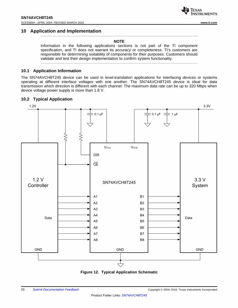
10 Application and Implementation
NOTEInformation in the following applications sections is not part of the TI componentspecification, and TI does not warrant its accuracy or completeness. TI’s customers areresponsible for determining suitability of components for their purposes. Customers shouldvalidate and test their design implementation to confirm system functionality.
10.1 Application InformationThe SN74AVCH8T245 device can be used in level-translation applications for interfacing devices or systemsoperating at different interface voltages with one another. The SN74AVCH8T245 device is ideal for datatransmission which direction is different with each channel. The maximum data rate can be up to 320 Mbps whendevice voltage power supply is more than 1.8 V.
10.2 Typical Application
Figure 12. Typical Application Schematic
Input(1.2V)
Output(3.3V)
1.2V to 3.3V Voltage Translation(2.5MHz)
21
SN74AVCH8T245www.ti.com SCES565H –APRIL 2004–REVISED MARCH 2016
Product Folder Links: SN74AVCH8T245
Submit Documentation FeedbackCopyright © 2004–2016, Texas Instruments Incorporated
Typical Application (continued)10.2.1 Design RequirementsFor this design example, use the parameters listed in Table 3.
Table 3. Design ParametersDESIGN PARAMETERS EXAMPLE VALUE
Input voltage 1.2 V to 3.6 VOutput voltage 1.2 V to 3.6 V
10.2.2 Detailed Design ProcedureTo begin the design process, determine the following:• Input voltage range
– Use the supply voltage of the device that is driving the SN74AVCH8T245 device to determine the inputvoltage range. For a valid logic high the value must exceed the VIH of the input port. For a valid logic lowthe value must be less than the VIL of the input port.
• Output voltage range– Use the supply voltage of the device that the SN74AVCH8T245 device is driving to determine the output
voltage range.
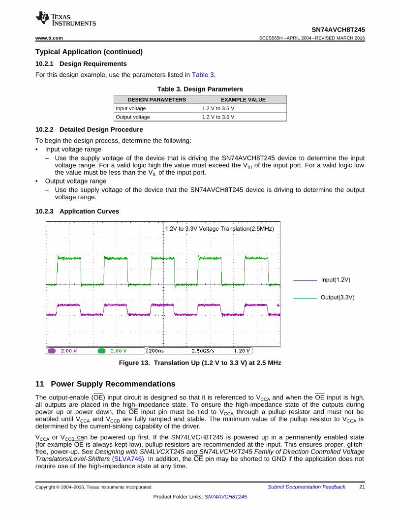
10.2.3 Application Curves
Figure 13. Translation Up (1.2 V to 3.3 V) at 2.5 MHz
11 Power Supply RecommendationsThe output-enable (OE) input circuit is designed so that it is referenced to VCCA and when the OE input is high,all outputs are placed in the high-impedance state. To ensure the high-impedance state of the outputs duringpower up or power down, the OE input pin must be tied to VCCA through a pullup resistor and must not beenabled until VCCA and VCCB are fully ramped and stable. The minimum value of the pullup resistor to VCCA isdetermined by the current-sinking capability of the driver.
VCCA or VCCB can be powered up first. If the SN74LVCH8T245 is powered up in a permanently enabled state(for example OE is always kept low), pullup resistors are recommended at the input. This ensures proper, glitch-free, power-up. See Designing with SN4LVCXT245 and SN74LVCHXT245 Family of Direction Controlled VoltageTranslators/Level-Shifters (SLVA746). In addition, the OE pin may be shorted to GND if the application does notrequire use of the high-impedance state at any time.
From
Controller
1
2
3
4
16
B1A2
DIR
OE
VCCB
A1
LEGEND
VIA to Power Plane
VIA to GND Plane (Inner Layer)
Polygonal Copper Pour
From
Controller
15
14
13
Bypass Capacitor
VCCA
5
6
7
12
12
GNDGND
A4
B4
A3 B2
B3
A5
11
10
13
VCCA
VCCB
Bypass Capacitor
From
Controller
To
System
To
System
SN74AVCH8T245
VCCA
Keep OE high until VCCA and
VCCB are powered upVCCB
From
Controller
From
Controller
To
System
To
System
8
9
10
12
A7
B7
A6 B5
B6
A8
11
10
From
Controller
To
System
From
Controller
From
Controller
To
System
To
System
11 GND B8 10To
System
22
SN74AVCH8T245SCES565H –APRIL 2004–REVISED MARCH 2016 www.ti.com
Product Folder Links: SN74AVCH8T245
Submit Documentation Feedback Copyright © 2004–2016, Texas Instruments Incorporated
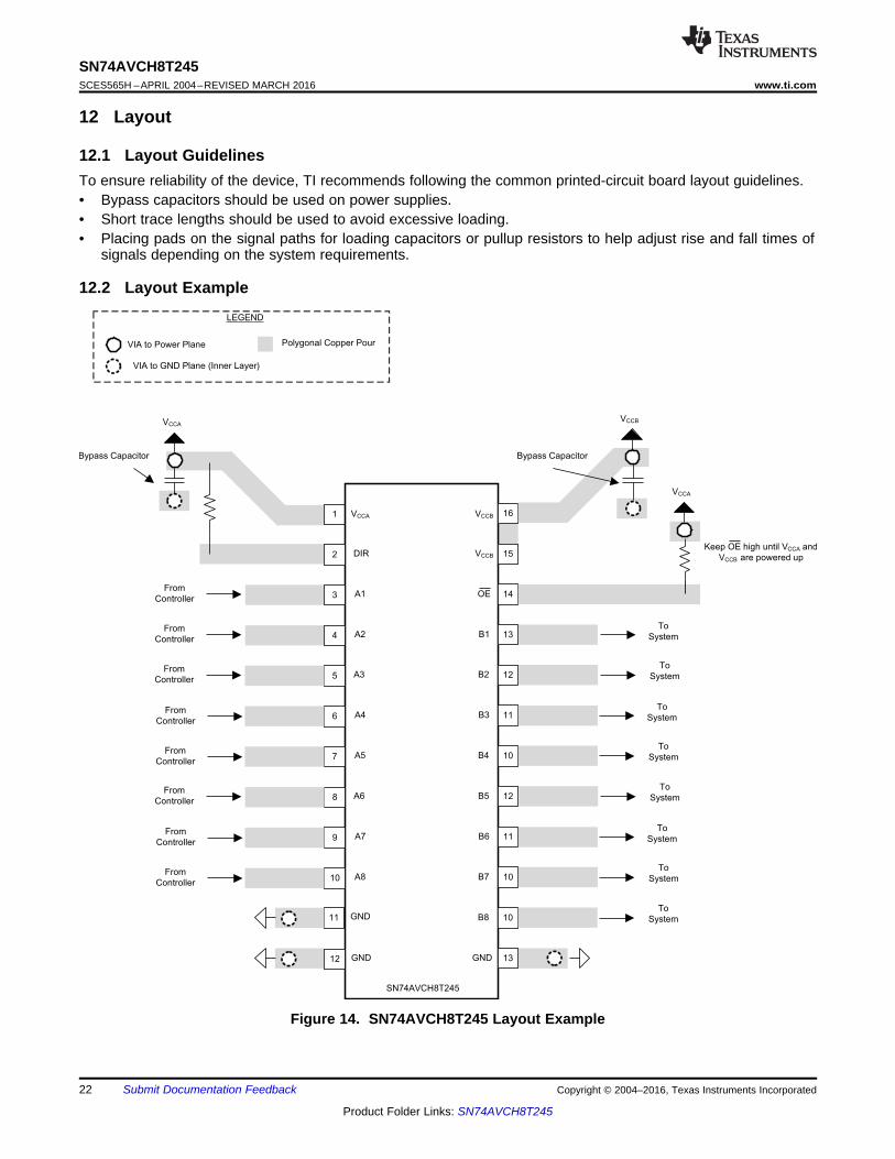
12 Layout
12.1 Layout GuidelinesTo ensure reliability of the device, TI recommends following the common printed-circuit board layout guidelines.• Bypass capacitors should be used on power supplies.• Short trace lengths should be used to avoid excessive loading.• Placing pads on the signal paths for loading capacitors or pullup resistors to help adjust rise and fall times of
signals depending on the system requirements.
12.2 Layout Example
Figure 14. SN74AVCH8T245 Layout Example
23
SN74AVCH8T245www.ti.com SCES565H –APRIL 2004–REVISED MARCH 2016
Product Folder Links: SN74AVCH8T245
Submit Documentation FeedbackCopyright © 2004–2016, Texas Instruments Incorporated
13 Device and Documentation Support
13.1 Documentation Support
13.1.1 Related DocumentationFor related documentation, see the following:• Designing with SN74LVCXT245 and SN74LVCHXT245 Family of Direction Controlled Voltage
Translators/Level-Shifters, SLVA746• Bus-Hold Circuit, SCLA015• AVC Logic Family Technology and Applications, SCEA006• CMOS Power Consumption and Cpd Calculation, SCAA035
13.2 Community ResourcesThe following links connect to TI community resources. Linked contents are provided "AS IS" by the respectivecontributors. They do not constitute TI specifications and do not necessarily reflect TI's views; see TI's Terms ofUse.
TI E2E™ Online Community TI's Engineer-to-Engineer (E2E) Community. Created to foster collaborationamong engineers. At e2e.ti.com, you can ask questions, share knowledge, explore ideas and helpsolve problems with fellow engineers.
Design Support TI's Design Support Quickly find helpful E2E forums along with design support tools andcontact information for technical support.
13.3 TrademarksE2E is a trademark of Texas Instruments.All other trademarks are the property of their respective owners.
13.4 Electrostatic Discharge CautionThese devices have limited built-in ESD protection. The leads should be shorted together or the device placed in conductive foamduring storage or handling to prevent electrostatic damage to the MOS gates.
13.5 GlossarySLYZ022 — TI Glossary.
This glossary lists and explains terms, acronyms, and definitions.
14 Mechanical, Packaging, and Orderable InformationThe following pages include mechanical, packaging, and orderable information. This information is the mostcurrent data available for the designated devices. This data is subject to change without notice and revision ofthis document. For browser-based versions of this data sheet, refer to the left-hand navigation.
PACKAGE OPTION ADDENDUM
www.ti.com 15-Jan-2016
Addendum-Page 1
PACKAGING INFORMATION
Orderable Device Status(1)
Package Type PackageDrawing
Pins PackageQty
Eco Plan(2)
Lead/Ball Finish(6)
MSL Peak Temp(3)
Op Temp (°C) Device Marking(4/5)
Samples
74AVCH8T245PWRG4 ACTIVE TSSOP PW 24 2000 Green (RoHS& no Sb/Br)
CU NIPDAU Level-1-260C-UNLIM -40 to 85 WP245
74AVCH8T245RHLRG4 ACTIVE VQFN RHL 24 1000 Green (RoHS& no Sb/Br)
CU NIPDAU Level-2-260C-1 YEAR -40 to 85 WP245
SN74AVCH8T245DGVR ACTIVE TVSOP DGV 24 2000 Green (RoHS& no Sb/Br)
CU NIPDAU Level-1-260C-UNLIM -40 to 85 WP245
SN74AVCH8T245PW ACTIVE TSSOP PW 24 60 Green (RoHS& no Sb/Br)
CU NIPDAU Level-1-260C-UNLIM -40 to 85 WP245
SN74AVCH8T245PWG4 ACTIVE TSSOP PW 24 60 Green (RoHS& no Sb/Br)
CU NIPDAU Level-1-260C-UNLIM -40 to 85 WP245
SN74AVCH8T245PWR ACTIVE TSSOP PW 24 2000 Green (RoHS& no Sb/Br)
CU NIPDAU Level-1-260C-UNLIM -40 to 85 WP245
SN74AVCH8T245RHLR ACTIVE VQFN RHL 24 1000 Green (RoHS& no Sb/Br)
CU NIPDAU Level-2-260C-1 YEAR -40 to 85 WP245
(1) The marketing status values are defined as follows:ACTIVE: Product device recommended for new designs.LIFEBUY: TI has announced that the device will be discontinued, and a lifetime-buy period is in effect.NRND: Not recommended for new designs. Device is in production to support existing customers, but TI does not recommend using this part in a new design.PREVIEW: Device has been announced but is not in production. Samples may or may not be available.OBSOLETE: TI has discontinued the production of the device.
(2) Eco Plan - The planned eco-friendly classification: Pb-Free (RoHS), Pb-Free (RoHS Exempt), or Green (RoHS & no Sb/Br) - please check http://www.ti.com/productcontent for the latest availabilityinformation and additional product content details.TBD: The Pb-Free/Green conversion plan has not been defined.Pb-Free (RoHS): TI's terms "Lead-Free" or "Pb-Free" mean semiconductor products that are compatible with the current RoHS requirements for all 6 substances, including the requirement thatlead not exceed 0.1% by weight in homogeneous materials. Where designed to be soldered at high temperatures, TI Pb-Free products are suitable for use in specified lead-free processes.Pb-Free (RoHS Exempt): This component has a RoHS exemption for either 1) lead-based flip-chip solder bumps used between the die and package, or 2) lead-based die adhesive used betweenthe die and leadframe. The component is otherwise considered Pb-Free (RoHS compatible) as defined above.Green (RoHS & no Sb/Br): TI defines "Green" to mean Pb-Free (RoHS compatible), and free of Bromine (Br) and Antimony (Sb) based flame retardants (Br or Sb do not exceed 0.1% by weightin homogeneous material)
(3) MSL, Peak Temp. - The Moisture Sensitivity Level rating according to the JEDEC industry standard classifications, and peak solder temperature.
(4) There may be additional marking, which relates to the logo, the lot trace code information, or the environmental category on the device.
PACKAGE OPTION ADDENDUM
www.ti.com 15-Jan-2016
Addendum-Page 2
(5) Multiple Device Markings will be inside parentheses. Only one Device Marking contained in parentheses and separated by a "~" will appear on a device. If a line is indented then it is a continuationof the previous line and the two combined represent the entire Device Marking for that device.
(6) Lead/Ball Finish - Orderable Devices may have multiple material finish options. Finish options are separated by a vertical ruled line. Lead/Ball Finish values may wrap to two lines if the finishvalue exceeds the maximum column width.
Important Information and Disclaimer:The information provided on this page represents TI's knowledge and belief as of the date that it is provided. TI bases its knowledge and belief on informationprovided by third parties, and makes no representation or warranty as to the accuracy of such information. Efforts are underway to better integrate information from third parties. TI has taken andcontinues to take reasonable steps to provide representative and accurate information but may not have conducted destructive testing or chemical analysis on incoming materials and chemicals.TI and TI suppliers consider certain information to be proprietary, and thus CAS numbers and other limited information may not be available for release.
In no event shall TI's liability arising out of such information exceed the total purchase price of the TI part(s) at issue in this document sold by TI to Customer on an annual basis.
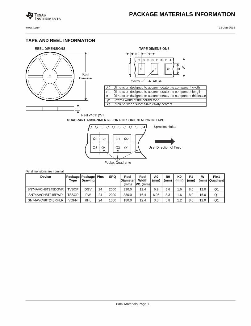
TAPE AND REEL INFORMATION
*All dimensions are nominal
Device PackageType
PackageDrawing
Pins SPQ ReelDiameter
(mm)
ReelWidth
W1 (mm)
A0(mm)
B0(mm)
K0(mm)
P1(mm)
W(mm)
Pin1Quadrant
SN74AVCH8T245DGVR TVSOP DGV 24 2000 330.0 12.4 6.9 5.6 1.6 8.0 12.0 Q1
SN74AVCH8T245PWR TSSOP PW 24 2000 330.0 16.4 6.95 8.3 1.6 8.0 16.0 Q1
SN74AVCH8T245RHLR VQFN RHL 24 1000 180.0 12.4 3.8 5.8 1.2 8.0 12.0 Q1
PACKAGE MATERIALS INFORMATION
www.ti.com 15-Jan-2016
Pack Materials-Page 1
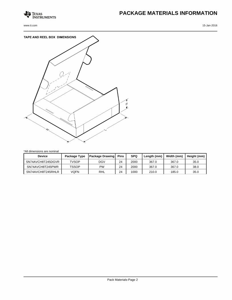
*All dimensions are nominal
Device Package Type Package Drawing Pins SPQ Length (mm) Width (mm) Height (mm)
SN74AVCH8T245DGVR TVSOP DGV 24 2000 367.0 367.0 35.0
SN74AVCH8T245PWR TSSOP PW 24 2000 367.0 367.0 38.0
SN74AVCH8T245RHLR VQFN RHL 24 1000 210.0 185.0 35.0
PACKAGE MATERIALS INFORMATION
www.ti.com 15-Jan-2016
Pack Materials-Page 2
IMPORTANT NOTICE
Texas Instruments Incorporated and its subsidiaries (TI) reserve the right to make corrections, enhancements, improvements and otherchanges to its semiconductor products and services per JESD46, latest issue, and to discontinue any product or service per JESD48, latestissue. Buyers should obtain the latest relevant information before placing orders and should verify that such information is current andcomplete. All semiconductor products (also referred to herein as “components”) are sold subject to TI’s terms and conditions of salesupplied at the time of order acknowledgment.TI warrants performance of its components to the specifications applicable at the time of sale, in accordance with the warranty in TI’s termsand conditions of sale of semiconductor products. Testing and other quality control techniques are used to the extent TI deems necessaryto support this warranty. Except where mandated by applicable law, testing of all parameters of each component is not necessarilyperformed.TI assumes no liability for applications assistance or the design of Buyers’ products. Buyers are responsible for their products andapplications using TI components. To minimize the risks associated with Buyers’ products and applications, Buyers should provideadequate design and operating safeguards.TI does not warrant or represent that any license, either express or implied, is granted under any patent right, copyright, mask work right, orother intellectual property right relating to any combination, machine, or process in which TI components or services are used. Informationpublished by TI regarding third-party products or services does not constitute a license to use such products or services or a warranty orendorsement thereof. Use of such information may require a license from a third party under the patents or other intellectual property of thethird party, or a license from TI under the patents or other intellectual property of TI.Reproduction of significant portions of TI information in TI data books or data sheets is permissible only if reproduction is without alterationand is accompanied by all associated warranties, conditions, limitations, and notices. TI is not responsible or liable for such altereddocumentation. Information of third parties may be subject to additional restrictions.Resale of TI components or services with statements different from or beyond the parameters stated by TI for that component or servicevoids all express and any implied warranties for the associated TI component or service and is an unfair and deceptive business practice.TI is not responsible or liable for any such statements.Buyer acknowledges and agrees that it is solely responsible for compliance with all legal, regulatory and safety-related requirementsconcerning its products, and any use of TI components in its applications, notwithstanding any applications-related information or supportthat may be provided by TI. Buyer represents and agrees that it has all the necessary expertise to create and implement safeguards whichanticipate dangerous consequences of failures, monitor failures and their consequences, lessen the likelihood of failures that might causeharm and take appropriate remedial actions. Buyer will fully indemnify TI and its representatives against any damages arising out of the useof any TI components in safety-critical applications.In some cases, TI components may be promoted specifically to facilitate safety-related applications. With such components, TI’s goal is tohelp enable customers to design and create their own end-product solutions that meet applicable functional safety standards andrequirements. Nonetheless, such components are subject to these terms.No TI components are authorized for use in FDA Class III (or similar life-critical medical equipment) unless authorized officers of the partieshave executed a special agreement specifically governing such use.Only those TI components which TI has specifically designated as military grade or “enhanced plastic” are designed and intended for use inmilitary/aerospace applications or environments. Buyer acknowledges and agrees that any military or aerospace use of TI componentswhich have not been so designated is solely at the Buyer's risk, and that Buyer is solely responsible for compliance with all legal andregulatory requirements in connection with such use.TI has specifically designated certain components as meeting ISO/TS16949 requirements, mainly for automotive use. In any case of use ofnon-designated products, TI will not be responsible for any failure to meet ISO/TS16949.
Products ApplicationsAudio www.ti.com/audio Automotive and Transportation www.ti.com/automotiveAmplifiers amplifier.ti.com Communications and Telecom www.ti.com/communicationsData Converters dataconverter.ti.com Computers and Peripherals www.ti.com/computersDLP® Products www.dlp.com Consumer Electronics www.ti.com/consumer-appsDSP dsp.ti.com Energy and Lighting www.ti.com/energyClocks and Timers www.ti.com/clocks Industrial www.ti.com/industrialInterface interface.ti.com Medical www.ti.com/medicalLogic logic.ti.com Security www.ti.com/securityPower Mgmt power.ti.com Space, Avionics and Defense www.ti.com/space-avionics-defenseMicrocontrollers microcontroller.ti.com Video and Imaging www.ti.com/videoRFID www.ti-rfid.comOMAP Applications Processors www.ti.com/omap TI E2E Community e2e.ti.comWireless Connectivity www.ti.com/wirelessconnectivity
Mailing Address: Texas Instruments, Post Office Box 655303, Dallas, Texas 75265Copyright © 2016, Texas Instruments Incorporated