Embed Size (px)
Citation preview

University of Birmingham
Reactive Power and AC Voltage Control of LCCHVDC System with Controllable CapacitorsXue, Ying; Zhang, Xiao-Ping
DOI:10.1109/TPWRS.2016.2557342
License:Creative Commons: Attribution (CC BY)
Document VersionPublisher's PDF, also known as Version of record
Citation for published version (Harvard):Xue, Y & Zhang, X-P 2017, 'Reactive Power and AC Voltage Control of LCC HVDC System with ControllableCapacitors', IEEE Transactions on Power Systems, vol. 31, no. 1, TPWRS-01743-2015, pp. 753.https://doi.org/10.1109/TPWRS.2016.2557342
Link to publication on Research at Birmingham portal
General rightsUnless a licence is specified above, all rights (including copyright and moral rights) in this document are retained by the authors and/or thecopyright holders. The express permission of the copyright holder must be obtained for any use of this material other than for purposespermitted by law.
•Users may freely distribute the URL that is used to identify this publication.•Users may download and/or print one copy of the publication from the University of Birmingham research portal for the purpose of privatestudy or non-commercial research.•User may use extracts from the document in line with the concept of ‘fair dealing’ under the Copyright, Designs and Patents Act 1988 (?)•Users may not further distribute the material nor use it for the purposes of commercial gain.
Where a licence is displayed above, please note the terms and conditions of the licence govern your use of this document.
When citing, please reference the published version.
Take down policyWhile the University of Birmingham exercises care and attention in making items available there are rare occasions when an item has beenuploaded in error or has been deemed to be commercially or otherwise sensitive.
If you believe that this is the case for this document, please contact [email protected] providing details and we will remove access tothe work immediately and investigate.
Download date: 14. Mar. 2020

This work is licensed under a Creative Commons Attribution 3.0 License. For more information, see http://creativecommons.org/licenses/by/3.0/.
This article has been accepted for publication in a future issue of this journal, but has not been fully edited. Content may change prior to final publication. Citation information: DOI 10.1109/TPWRS.2016.2557342, IEEETransactions on Power Systems
> REPLACE THIS LINE WITH YOUR PAPER IDENTIFICATION NUMBER (DOUBLE-CLICK HERE TO EDIT) <
1
Abstract—It is well-known that traditional LCC HVDC system
is not able to control its reactive power and terminal AC voltages.
This paper investigates the reactive power and AC voltage
control at the inverter side of the LCC HVDC system with
controllable capacitors. The system’s ability of operating under
negative extinction angle is utilized to achieve a wide range of
reactive power control and, in particular, the ability of exporting
reactive power. In connection with the inverter AC terminal
voltage or reactive power control, among different control
possibilities at the rectifier side, active power control is desirable
since large variations of active power transfer is very
unfavorable. Detailed theoretical analysis is carried out first to
show the reactive power controllability, and the capacitor voltage
level is selected based on the desired control range. In addition, a
new extinction angle measurement approach is proposed for
negative extinction angle measurements. The effectiveness of the
reactive power/voltage control capability for the proposed system
is validated through simulation results using Real Time Digital
Simulator (RTDS). To verify the effectiveness of the reactive
power and voltage control, CCC HVDC and LCC HVDC with
SVC are also set up in RTDS, and simulation comparisons are
made. Furthermore, contribution to AC voltage control in power
system using the proposed method is demonstrated through
simulation results on the modified two-area four-machine AC
power system.
Index Terms—reactive power control, AC voltage control,
LCC HVDC, HVDC with controllable capacitor, HVDC
transmission.
I. INTRODUCTION
RADITIONAL Line-Commutated Converter (LCC) based
High Voltage Direct Current (HVDC) technology has
played an important role in long distance bulk power
transmission around the world since its first application 60
years ago. However some well-known limitations associated
with it still exist today which to a certain extent limit further
applications of such a technology. One of the limitations is
significant reactive power requirement at both sides of the
HVDC system. The reactive power requirement originates
from the firing of thyristors after commutation voltage
becomes positive, which in effect delayed the current
waveforms with respect to the voltage waveforms [1]. So both
rectifier and inverter sides of the system absorb reactive
This work was sponsored by EPSRC Grant EP/L017725/1.
The authors are with the Department of Electronic, Electrical and Systems
Engineering, University of Birmingham, Edgbaston, Birmingham, B15 2TT, U.K. (e-mail: [email protected]).
power. However it should be noted that to the sending end AC
system, the rectifier represents a load and it is natural that it
draws some reactive power from the network just like other
loads. On the other hand, from the point of view of the
receiving end AC system, the inverter acts as a power
producer and as such should take its share of reactive load.
But the reality is that instead of producing, the inverter
consumes reactive power thus its consumption level of
reactive power should be minimized. Furthermore, with
passive reactive power compensation at the inverter side, the
level of reactive power being produced tends to decrease
under transient AC voltage drops where reactive power
support is needed most. At the same time, the minimum
extinction angle controller will advance its firing angle which
leads to a higher reactive power consumption and causes
further AC voltage drops. These operational characteristics are
clearly unfavorable, and FACTS devices such as STATCOM
and SVC, etc may be needed to mitigate the problem.
In contrast to what has been described above, the desired
inverter performances can be listed as follows:
Very low or zero reactive power consumption level at
steady-state.
AC voltage control by inverter itself especially under
large AC disturbances.
It should be pointed out that the reactive power or voltage
controllability at the inverter side should not be achieved at
the expense of reduced active power transfer level, as the
primary role of an HVDC link is to provide a stable active
power transfer. In this way, the advantage of the inverter
reactive power control can be maximized.
For a back-to-back LCC HVDC scheme it is possible to
design reactive power controller at the inverter side to control
its reactive power consumption [2, 3]. In this case since the
two converter stations are located on the same site, the
problems of communication delay and the risk of loss of
communications between rectifier and inverter control systems
are minimized. Also the measurements from both terminals
are readily available for both control systems. Hence it is
possible for the inverter to control its reactive power
consumption by varying its extinction angle while the danger
of losing commutation margin can be mitigated by the rectifier
controller modifying its operating conditions. This type of
control helps improve the AC voltage stability at the inverter
bus by controlling reactive power consumption, but
considerable steady state reactive power consumption still
remains. In addition this type of control strategy is limited to
Ying Xue, Xiao-Ping Zhang, Senior Member, IEEE
Reactive Power and AC Voltage Control of LCC
HVDC System with Controllable Capacitors
T

This work is licensed under a Creative Commons Attribution 3.0 License. For more information, see http://creativecommons.org/licenses/by/3.0/.
This article has been accepted for publication in a future issue of this journal, but has not been fully edited. Content may change prior to final publication. Citation information: DOI 10.1109/TPWRS.2016.2557342, IEEETransactions on Power Systems
> REPLACE THIS LINE WITH YOUR PAPER IDENTIFICATION NUMBER (DOUBLE-CLICK HERE TO EDIT) <
2
back-to-back HVDC schemes.
For point to point HVDC schemes, unlike back-to-back
schemes, the communication delay and/or the requirements for
the system to operate without communications largely limit
the possibility of reactive power control. Most of the
literatures are then focused on reactive power compensation
rather than reducing reactive consumption level of converter
[4-12]. In those methods, external reactive compensation
devices are installed at the inverter AC side. It is well known
that a LCC inverter could not control its reactive power
consumption because the extinction angle cannot be desirably
small in order to ensure sufficient commutation margin in case
of disturbances on the inverter AC side. Hence, various
methods of managing and optimizing the externally installed
reactive compensation devices have been investigated so as to
support the operation of the LCC Inverter [13-15].
One of the promising methods which can operate with
better power factor angle is the Capacitor Commutated
Converter (CCC) based HVDC [16-20]. Depending on the size
of capacitors, the phase shift introduced by these capacitors to
the valve side commutation voltage can be such that the
inverter side is able to achieve around 10%-15% reactive
power consumption. However this usually requires large
capacitors which significantly increase valve voltage stress
and costs [21].
This paper focuses on achieving the aforementioned desired
inverter performances by further exploiting the reactive power
control capability of the previously proposed LCC HVDC
system with controllable capacitors [22]. Since capacitor
insertions change the dynamic behavior of the inverter,
theoretical analysis need to be carried out to investigate the
reactive power controllability. The effects of capacitor
insertions have on the system variables are calculated for the
first time. Then the inverter power factor as a function of
extinction angle is calculated and is used to demonstrate the
controllability. Finally with theoretical analysis as the basis,
controllers are designed to validate the reactive power and AC
voltage control performances.
The rest of the paper is organized as follows. Section II
briefly reviews the system configuration and explains its
operational concepts. Section III analytically derives how
reactive power is related to other system variables. Section IV
presents the proposed extinction angle measurement, the
designed reactive power controller and inverter AC voltage
controller. Section V firstly shows the simulation results of
reactive power control and inverter AC voltage control,
respectively, of the proposed system using the modified
CIGRE benchmark system. Comparisons with CCC HVDC
are made. Then the simulation results of applying the
proposed method in two-area four-machine system are
presented. After that further comparisons with LCC HVDC
with SVC are made. All simulations are carried out using Real
Time Digital Simulator (RTDS). Finally concluding remarks
are given in section VI.
II. SYSTEM CONFIGURATION & OPERATIONAL CONCEPTS
A. System Configuration
The LCC HVDC system with controllable capacitors [16]
and the connected AC system at the inverter side are shown in
Fig. 1. In the figure, TY1-TY6 and TD1-TD6 are thyristor
valves, CapYa, CapYb, CapYc and CapDa, CapDb, CapDc are
capacitor modules, S1Ya-S4Ya are four Insulated Gate Bipolar
Transistor (IGBT) switches for capacitor module CapYa. The
system is based on the CIGRE HVDC Benchmark model with
all the system parameters got from [23]. An induction machine
is added to the inverter AC bus to test the AC voltage
controller performance. Capacitor modules are connected in
series between the secondary side of converter transformers
and thyristor valves. Each capacitor module can be realized by
a single module (as that for 2-level VSC) or by a number of
series connected sub-modules to achieve higher insertion
voltage. Each module consists of four IGBT switches with
anti-parallel diode across each one of them. The reference
polarity of the capacitor is shown in Fig. 1(b). Each capacitor
module will be inserted as a positive voltage when S1 and S4
are switched on and S2 and S3 are switched off, and will be
inserted as a negative voltage when S2 and S3 are switched on
and S1 and S4 are switched off. Bypass is achieved by
switching S1 and S3 on or S2 and S4 on at the same time.
CapYa
CapYb
CapYcY-Y
TY1
TY2
TY3
TY4
TY5
TY6
Inverter AC busIdc Ls
CapDa
CapDb
CapDcD-Y
TD1
TD2
TD3
TD4
TD5
TD6
a
b
c
a
b
c
AC sourceZinv
Zfilter
IM
Tr3
Circuit
Breaker
(a)
S1Ya
S2Ya
S3Ya
S4Ya
+
-C1
CapYa
To valve
side
To transformer
secondary side
(b)
Fig. 1. Configuration of LCC HVDC system with controllable capacitors. (a)
Inverter and connected AC system; (b) Capacitor module configuration.
B. Insertion Strategy
The so called ‘push’ & ‘pull’ insertion strategy works by
inserting capacitor modules into the two commutating phases
during commutation. The polarities of the inserted capacitors
are such that the voltages provided by them are in favor of the
commutation process. For example for the commutation from
TY2 to TY4 as shown Fig. 2, CapYc is inserted as a positive
voltage and CapYa is inserted as a negative voltage until the

This work is licensed under a Creative Commons Attribution 3.0 License. For more information, see http://creativecommons.org/licenses/by/3.0/.
This article has been accepted for publication in a future issue of this journal, but has not been fully edited. Content may change prior to final publication. Citation information: DOI 10.1109/TPWRS.2016.2557342, IEEETransactions on Power Systems
> REPLACE THIS LINE WITH YOUR PAPER IDENTIFICATION NUMBER (DOUBLE-CLICK HERE TO EDIT) <
3
commutation is complete. CapYb in phase B is in bypass mode
during this commutation process. This additional commutation
voltage from the inserted capacitors guarantees the successful
commutations when inverter is exporting reactive power. It
should be mentioned that compared with CCC HVDC, since
the controllable capacitors are mainly inserted into the circuit
during commutation period, valve voltage stress is slightly
increased, and is comparable to the original LCC HVDC
system [22].
CapYc
TY2
TY3
TY4
AC
- +
+ -
CapYa
a
b
c
3i
2i
4icL
cL
cL
Id
Fig. 2. Commutation from TY2 to TY4.
C. Capacitor Voltage Balancing
PI
Controller
_c refV
measVYYa+
-
YYa
-/+ zero
crossing
detector
Q
QSET
CLR
S
RPLL
FPYYaPos
TY4 +/- zero
crossing
‘Push’ & ‘Pull’
firing logics
YYa +
-
Fig. 3. Capacitor voltage balancing logics.
The balancing of capacitors takes place when one of the two
thyristor valves connected to that specific phase is conducting.
Considering the balancing of CapYa, it can be charged or
discharged when TY4 or TY1 is fully conducting. The designed
balancing strategy inserts CapYa as a positive voltage before
the firing of TY6 and bypasses it when the commutation from
TY4 to TY6 is complete. The main control logics for CapYa
balancing are shown in Fig. 3 where and are
the measured and reference values for CapYa voltage, is
the phase reference for actual insertion time and FPYYaPos is
the switching word. It can be seen that the control angle
at which CapYa is inserted is generated by minimizing its
voltage error signal through a PI controller. The actual
switching word is determined by comparing the
control angle with the relevant phase information from PLL.
The voltage balancing logics of all the other capacitor modules
have the similar structure but with different phase information.
It is worth mentioning that for the CCC HVDC where
capacitor voltages are not controlled, unbalanced capacitor
voltages can appear during unbalanced faults. This can add
additional complexity to the control system. However for the
proposed system where capacitor voltages are actively
controlled, they can stay balanced during unbalanced fault,
and therefore reduce the complexity of control system.
III. THEORETICAL ANALYSIS OF REACTIVE POWER
CONTROLLABILITY
This section is to examine the reactive power controllability
by capacitor insertion and firing angle control. The capacitor
insertion strategy and capacitor voltage balancing actions
affect the system from three different aspects. Firstly the
overlap angle is smaller due to additional commutation
voltage from capacitors. Secondly the average voltage across
the 6-pulse bridge is increased due to the difference of
capacitor voltage change during commutation. Thirdly the pre-
insertion of capacitors for charging purpose also increases the
average bridge voltage. In the following, analytical derivations
will be presented for all three aspects and then variation of
power factor (interchangeably variation of reactive power) as
a function of firing angle and extinction angle will be shown.
In addition, selection of capacitor voltage level for the desired
operating range is also presented.
A. Commutation Overlap
TY2
TY3
AC
- +
+ -
a
b
c
TY1
cL
dI
dI
1i
3i
2i
cL
cL
nv
pv
Fig. 4. Commutation from TY1 to TY3.
The commutation period from TY1 to TY3 as shown in Fig.
4 is considered in this section where cL is the transformer
leakage inductance, C is the capacitor value, nv is the
instantaneous voltage for the capacitor inserted in negative
direction and pv is the instantaneous voltage for the capacitor
inserted in in positive direction, 1i and 3i are instantaneous
currents flowing through TY1 and TY3, respectively. The
instantaneous line-to-neutral source voltages are
cos 60
cos 60
cos 180
a m
ob m
om
o
c
e E t
e E t
e E t
(1)
where is the phase voltage magnitude and is the rated
system angular frequency. Dynamic equations for the
commutation loop can be written as [22]
1 3 di i I (2)
1ndv
i Cdt
(3)
3
pdvi C
dt (4)
3 1
b c p a c n
di die L v e L v
dt dt (5)
With initial conditions

This work is licensed under a Creative Commons Attribution 3.0 License. For more information, see http://creativecommons.org/licenses/by/3.0/.
This article has been accepted for publication in a future issue of this journal, but has not been fully edited. Content may change prior to final publication. Citation information: DOI 10.1109/TPWRS.2016.2557342, IEEETransactions on Power Systems
> REPLACE THIS LINE WITH YOUR PAPER IDENTIFICATION NUMBER (DOUBLE-CLICK HERE TO EDIT) <
4
/|p t ov t V (6)
/ 3
1| | 0
p
tt
dv ti
dt C
(7)
where is the firing angle and oV is the initial charged
capacitor voltage. By solving (2)-(5), pv and 3i can be
obtained as follows [22]:
21p n nv C cos t C sin t Bsin t D (8)
3 1 2( sin cos cos )2
dn n n n
Ii C C t C t B t
C (9)
where
1 02
d
nn
bI BbC aV Basin cos
C
(10)
022
d
nn
aI BaC bV Bbsin cos
C
(11)
cos na
(12)
sin nb
(13)
1
n
cL C (14)
2 2
3 1
2
m
c n
EB
L C
(15)
2 2
d dI ID t
C C
(16)
Since at the end of commutation t
and 3 di I
(where is the overlap angle),
1 2( sin cos
cos )2
d n n n n
d
I C C C
IB
C
(17)
Using the parameters from Benchmark model and C of
585 F , overlap angle can be calculated as a function of
capacitor voltage levels for different firing angles by solving
(17). The capacitor value of 585 uF is the same as that
calculated in [22] so that the level of capacitor voltage change
is not significant after each commutation. It can be seen from
Fig. 5 that as capacitor voltage increases, overlap angle
reduces to about010 and does not vary significantly for
different firing angles.
Fig. 5 Variation of overlap angle against capacitor voltage for different firing
angles.
B. Pre-insertion of Capacitors
The duration of pre-insertion of capacitors depends on the
level of its voltage reduction over a cycle. For the same
commutation period from TY1 to TY3, the voltage increase in
the outgoing phase is
0( )in nV v V
(18)
and the voltage decrease in the incoming phase is
0 ( )de pV V v
(19)
By substituting (3) and (4) into (2) and then integrate over
the whole commutation period gives
( ) ( ) dn p
Iv v
C
(20)
Since for one cycle each capacitor voltage increases and
decreases two times so the net decrease of voltage is
2 2total de inV V V (21)
Substituting (18)-(20) into (21),
0
24 4 ( ) d
total p
IV V v
C
(22)
Hence the pre-insertion time required per cycle is
total
d
V Ct
I
(23)
Therefore the average voltage increase due to the pre-
insertion of capacitor is
0
2
totalpre
d
V V CV
I
(24)
C. Commutation
For the same commutation period from TY1 to TY3, the
bridge lower point voltage during commutation is
( ) ( )
2
a n b p
low
e v e vV
(25)
So the average voltage increase over a cycle due to the
bridge voltage increase during commutation is
( ) ( )
2 2 3
a n b pa be v e ve e
V dt dt
(26)
Considering (2)-(3), (26) can be simplified to
2
2
3
4
dIV
C
(27)
Similar to (24), V can be calculated once overlap angle is
solved.
D. Power Factor
Without capacitor insertions the average DC voltage is
given by
3 6 cos( ) cos( )
2original LNV E
(28)
80 90 100 110 120 130 140 1505
10
15
20
25
Capacitor Voltage (kV)
Ove
rlap
An
gle
(de
g)
alpha=153
alpha=163
alpha=173
This work is licensed under a Creative Commons Attribution 3.0 License. For more information, see http://creativecommons.org/licenses/by/3.0/.
This article has been accepted for publication in a future issue of this journal, but has not been fully edited. Content may change prior to final publication. Citation information: DOI 10.1109/TPWRS.2016.2557342, IEEETransactions on Power Systems
> REPLACE THIS LINE WITH YOUR PAPER IDENTIFICATION NUMBER (DOUBLE-CLICK HERE TO EDIT) <
5
where LNE is the RMS line-to-neutral voltage.
Hence the average DC voltage with capacitor insertions is
| |d original preV V V V (29)
(a)
(b)
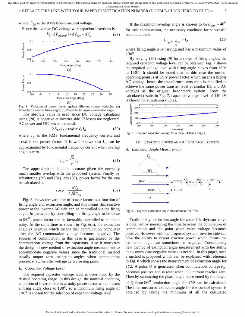
Fig. 6 Variation of power factor against different control variables. (a) Powerfactor against firing angle; (b) Power factor against extinction angle.
The absolute value is used since DC voltage calculated
using (28) is negative at inverter side. If losses are neglected,
AC power and DC power are equal:
13 cosLN L d dE I V I (30)
where 1LI is the RMS fundamental frequency current and
cos is the power factor. It is well known that 1LI can be
approximated by fundamental frequency current when overlap
angle is zero
1
6L dI I
(31)
The approximation is quite accurate given the normally
much smaller overlap with the proposed system. Finally by
substituting (29) and (31) into (30), power factor for the can
be calculated as
cos3 6
d
LN
V
E
(32)
Fig. 6 shows the variation of power factor as a function of
firing angle and extinction angle, and this means that reactive
power at the inverter AC side can be controlled via the firing
angle. In particular by controlling the firing angle to be close
to0180 , power factor can be favorably controlled to be about
unity. At the same time as shown in Fig. 6(b), the extinction
angle is negative which means that commutation completes
after the AC commutation voltage becomes negative. The
success of commutation in this case is guaranteed by the
commutation voltage from the capacitors. Also it motivates
the design of new method of extinction angle measurement to
accommodate negative values since the traditional method
usually output zero extinction angles when commutation
process stretches after voltage zero crossing point.
E. Capacitor Voltage Level
The required capacitor voltage level is determined by the
desired operating range. In this design, the nominal operating
condition of inverter side is at unity power factor which means
a firing angle close to , so a maximum firing angle of
is chosen for the selection of capacitor voltage level.
If the maximum overlap angle is chosen to be0
max 40
for safe commutation, the necessary condition for successful
commutation is
max3 | d
ti I
(33)
where firing angle is varying and has a maximum value of
.
By solving (33) using (9) for a range of firing angles, the
required capacitor voltage level can be obtained. Fig. 7 shows
the required voltage level with firing angle ranges from
to . It should be noted that in this case the normal
operating point is at unity power factor which means a higher
AC voltage, hence the transformer turns ratio is modified to
achieve the same power transfer level at similar DC and AC
voltages as the original benchmark system. From the
calculated results in Fig. 7, capacitor voltage level of 110 kV
is chosen for simulation studies.
Fig. 7. Required capacitor voltage for a range of firing angles.
IV. REACTIVE POWER AND AC VOLTAGE CONTROL
A. Extinction Angle Measurement
Q
QSET
CLR
S
R
caV
Q
Q
t
t
t
t
t
2ITY
1Pulse
2Pulse
Timer
2_TY measQt
+
-
Fig. 8. Proposed extinction angle measurement for TY2.
Traditionally, extinction angle for a specific thyristor valve
is obtained by measuring the time between the completion of
commutation and the point when valve voltage becomes
positive. However with the proposed system, inverter side can
have the ability to export reactive power which means the
extinction angle can sometimes be negative. Consequently
new method of extinction angle measurement with the ability
to accommodate negative values is needed. In this paper, such
a method is proposed which can be explained with reference
to Fig. 8 which shows the measurement of extinction angle for
TY2. A pulse Q is generated when commutation voltage cae
becomes positive and is reset when TY2 current reaches zero.
Then by subtracting the phase angle represented by the length
of Q from0180 , extinction angle for TY2 can be calculated.
The final measured extinction angle for the control system is
obtained by taking the minimum of all the calculated
140 145 150 155 160 165 170 1750.8
0.9
1
Firing Angle (Deg)
Pow
er
Facto
r
-10 -5 0 5 10 15 20 25 30 350.8
0.9
1
Extinction Angle (Deg)
Pow
er
Facto
r
160 165 170 175 180 185 1900
50
100
150
alpha (deg)C
apacitor
Voltage (
kV
)
This work is licensed under a Creative Commons Attribution 3.0 License. For more information, see http://creativecommons.org/licenses/by/3.0/.
This article has been accepted for publication in a future issue of this journal, but has not been fully edited. Content may change prior to final publication. Citation information: DOI 10.1109/TPWRS.2016.2557342, IEEETransactions on Power Systems
> REPLACE THIS LINE WITH YOUR PAPER IDENTIFICATION NUMBER (DOUBLE-CLICK HERE TO EDIT) <
6
extinction angles for all the valves. In this way, negative
extinction angle can be measured which enables the design of
reactive power feedback controller.
PI
Controller
PI
Controller refQ
measQmeas
errorQ ordererror
CE
inv+
- +
--
maxinv
mininv
Fig. 9. Proposed inverter reactive power controller.
PI
Controller refV
measV
inv+
-
max
min
Fig. 10 Proposed Inverter AC voltage controller.
MinPI
Controller refP
_dc measV
orderIrec
+
-
maxrec
minrec
VDCOLI measI
Fig. 11 Rectifier active power controller
B. Reactive Power Controller
From theoretical analysis, it can be seen that reactive power
can be favorably controlled. Since the original inverter side is
using minimum extinction angle control, the reactive power
controller can be designed as such that the extinction angle
order is generated by an outer reactive power control loop
rather than a constant. Fig. 9 shows the proposed reactive
power controller at inverter side where , and
are reactive power reference, measurement and error
signals, respectively; , and are extinction
angle order, measurement and error, respectively; CE is the
inverter current error signal and is the inverter firing
angle. It can be seen that extinction angle reference is
generated by minimizing the reactive power error by a PI
controller. Ideally the extinction angle order can be calculated
from reactive power reference based on equations from
section III. However due to the highly nonlinear relationship
between extinction angle and reactive power, PI controller is
applied. Note that since the extinction angle measurement can
be negative, the controller is able to control the inverter
terminal to export reactive power if needed.
C. AC Voltage Controller
To control the AC voltage at the inverter AC bus, an AC
voltage controller can be designed utilizing the reactive power
controllability of the proposed system. In this case, the AC
voltage is controlled by controlling the reactive power
import/export of the inverter station. Therefore the inverter
AC voltage stability can be improved. The proposed inverter
controller is shown in Fig. 10 where and are
inverter AC voltage reference and measured values,
respectively. As can be seen from Fig. 10, a PI controller is
used to generate inverter firing angle by minimizing AC
voltage error.
D. Rectifier Active Power Control
As discussed before that it is important to ensure that active
power transfer of the DC system is kept at desired values
when inverter is controlling reactive power/AC voltage. Such
operational behavior is achieved by utilizing rectifier side
controller to control active power transfer. Fig. 11 shows the
active power controller being applied at rectifier side. The
active power reference is divided by DC voltage
measurement to get the desired current, and the DC
current order signal is obtained by taking the minimum
value of desired current and current order from VDCOL-
. Finally PI controller is used to generate the control
input of firing angle .
The parameters for the above PI controllers are selected by
trial and error through simulation studies.
V. SIMULATION RESULTS
This section presents the simulation results of reactive
power control and inverter AC voltage control of the LCC
HVDC system with controllable capacitors. The nominal
operating point for both cases is designed so that the inverter
side is absorbing zero reactive power and sending rated active
power at rated DC and AC voltages. The capacitor banks are
removed and transformer turns ratio is modified to meet the
rated working condition. The values of capacitors are
and its voltage level is chosen to be 110 kV. The rectifier side
is controlling the active power transfer by controlling the DC
current. The AC systems at both sides are kept the same as the
CIGRE HVDC benchmark model. The whole system is
modelled in RTDS with a small simulation time-step of .
A. Reactive Power Control
Fig. 12 shows the system responses following changes of
reactive power reference. In this simulation, the reactive
power reference is initially set to zero and changes to -150
MVar at 3.1s, then increases to 150 MVar at 4.6s and finally
changes back to zero at 6.1s. Negative reactive power
indicates that the inverter is exporting reactive power to the
AC system.
(a)
(b)
2.5 3 3.5 4 4.5 5 5.5 6 6.5 7 7.5 8-400
-200
0
200
400
Time (s)
Reactive P
ow
er
(MV
ar)
3 4 5 6 7 8
500
1000
Time (s)
Pow
er
(MW
)

This work is licensed under a Creative Commons Attribution 3.0 License. For more information, see http://creativecommons.org/licenses/by/3.0/.
This article has been accepted for publication in a future issue of this journal, but has not been fully edited. Content may change prior to final publication. Citation information: DOI 10.1109/TPWRS.2016.2557342, IEEETransactions on Power Systems
> REPLACE THIS LINE WITH YOUR PAPER IDENTIFICATION NUMBER (DOUBLE-CLICK HERE TO EDIT) <
7
(c)
(d)
(e)
(f)
(g)
(h)
(i)
Fig. 12. System responses with reactive power reference step changes. (a)
Reactive power consumption at inverter; (b) Active power transfer; (c) DC
voltage; (d) DC current; (e) Inverter firing angle; (f) Extinction angle; (g)
Capacitor voltages (CapYYa, CapYYb, CapYYc); (h) Capacitor currents for
CapYYa, CapYYb and CapYYc; (i) Zoomed in version of capacitor currents.
+
-
Vinv
QYY_sec
=140.1 MVar
Id
QYY_valve
=20.9 MVar
QYD_sec
=141.6 MVar
QYD_valve
=21.7 MVar
Q_converter
=150.1 MVarY-Y
D-Y
QYY_pri
=75.5 MVar
QYD_pri
=74.6 MVar
6-pulse
bridge
Fig. 13. Reactive power flow distribution when the inverter is exporting
reactive power.
It can be seen from Fig. 12(a) that measured reactive power
successfully tracks the reference and is able to achieve zero
steady-state reactive power consumption. It can also be
observed that inverter can export reactive power if needed. At
the same time, active power transfer on the DC link is
controlled at the rated value which is shown in Fig. 12(b). The
response of the DC active power at the instants of step
changes of the reactive power can be explained by considering
controller actions. For example when the reactive power
reference is increased, the inverter firing angle is decreased
according to the controller shown in Fig. 9. This decrease of
inverter firing angle leads to a decrease of the DC voltage.
Therefore the DC power drops transiently as the DC current
cannot be changed instantly. Similarly when the reactive
power reference is decreased, there is a transient increase of
the DC active power. Since the change of the reactive power is
achieved by modifying the firing angles, the DC voltage also
changes. Both the inverter firing angle and the DC voltage are
shown in Fig. 12(e) and Fig 12(c). Fig. 12(d) shows that the
DC current is slightly changed to keep a constant active power
level and in Fig. 12(f) the corresponding changes in extinction
angle are shown. Negative values of the extinction angle
validate the effectiveness of the proposed method to measure
the negative extinction angle. The success of commutations
with a negative extinction angle is due to the additional
commutation voltages from the inserted capacitors [22].
Finally the voltage and current for the controllable capacitors
throughout the simulation period are shown in Fig. 12(g) and
Fig. 12(h), respectively. From Fig. 12(g) it can be seen that the
capacitor voltages are well balanced by the capacitor voltage
controller. Fig. 12(i) is the zoomed in version of Fig. 12(h)
which shows how the capacitor currents charge and discharge
the capacitors.
To further illustrate the reactive power flow distribution
when the inverter is exporting reactive power, Fig. 13 is
included where the inverter is controlled to export 150 MVar
of reactive power. In Fig. 13, QYY_valve and QYD_valve are
reactive power flows between the valve side and controllable
capacitors for upper and lower 6-pulse bridges, respectively;
QYY_sec and QYD_sec are the reactive power flows between
the secondary side of converter transformer and controllable
capacitor for the upper and lower 6-pulse bridges, respectively;
QYY_pri and QYD_pri are the reactive power flows at primary
side of converter transformer for the upper and lower 6-pulse
3 4 5 6 7 8
200
400
600
800
Time (s)
DC
voltage (
kV
)
3 4 5 6 7 8-2
0
2
4
Time (s)
Curr
ent
(kA
)
3 4 5 6 7 8
150
200
Time (s)
Firin
g a
ngle
(deg)
2.5 3 3.5 4 4.5 5 5.5 6 6.5 7 7.5 8-30
-20
-10
0
10
Time (s)
Extinction a
ngle
(deg)
3 4 5 6 7 8-50
0
50
100
150
Time (s)
Ca
pa
cito
r vo
lta
ge
(kV
)
CapYYa
CapYYb
CapYYc
3 4 5 6 7 8
-5
0
5
Time (s)
Ca
pa
cito
r C
urr
en
t (k
A)
ICYYa ICYYb ICYYc
4.875 4.88 4.885 4.89 4.895 4.9 4.905
-5
0
5
Time (s)
Ca
pa
cito
r C
urr
en
t (k
A)
ICYYa ICYYb ICYYc

This work is licensed under a Creative Commons Attribution 3.0 License. For more information, see http://creativecommons.org/licenses/by/3.0/.
This article has been accepted for publication in a future issue of this journal, but has not been fully edited. Content may change prior to final publication. Citation information: DOI 10.1109/TPWRS.2016.2557342, IEEETransactions on Power Systems
> REPLACE THIS LINE WITH YOUR PAPER IDENTIFICATION NUMBER (DOUBLE-CLICK HERE TO EDIT) <
8
bridges, respectively; Q_converter is the total inverter reactive
power output; is the DC current; is the inverter AC bus
voltage. The values shown in Fig. 13 are the averaged reactive
power flows. It can be seen that in this case both 6-pulse
bridges are exporting reactive power. This is because the
fundamental component voltage lags the fundamental
component current when the extinction angle is negative. This
export of reactive power is then increased by the reactive
power generated from the controllable capacitors. Finally the
net reactive power export of the inverter is obtained by
including the transformer reactive power consumption.
B. AC Voltage Control
This case study is used to demonstrate the inverter AC
voltage controllability following large inductive load changes.
The inverter side is using the proposed AC voltage controller.
The load being considered in this case study is an induction
machine with a rating of 98.5 MVA and a power factor of
0.94. It is connected to the inverter AC bus and is switched in
and out by controlling the connected circuit breakers.
(a)
(b)
(c)
(d)
(e)
(f)
(g)
(h)
(i)
Fig. 14. System responses with large inductive load switching. (a) Inverter
AC bus voltage; (b) Inverter reactive power consumption; (c) Active power
transfer; (d) Induction machine reactive power; (e) DC current; (f) Inverter
firing angle; (g) Capacitor voltages (CapYYa, CapYYb, CapYYc); (h)
Capacitor currents for CapYYa, CapYYb and CapYYc; (i) Zoomed in version
of capacitor currents.
(a)
(b)
(c)
0.1 0.2 0.3 0.4 0.5 0.6 0.7 0.8 0.9 1
180
200
220
240
260
280
Time (s)
AC
voltage (
kV
)
0.1 0.2 0.3 0.4 0.5 0.6 0.7 0.8 0.9 1
-500
0
500
Time (s)
Reactive P
ow
er
(MV
ar)
0.1 0.2 0.3 0.4 0.5 0.6 0.7 0.8 0.9 1
800
1000
1200
Time (s)
Active P
ow
er
(MW
)
0.1 0.2 0.3 0.4 0.5 0.6 0.7 0.8 0.9 1-100
0
100
200
Time (s)
Reactive P
ow
er
(MV
ar)
0.1 0.2 0.3 0.4 0.5 0.6 0.7 0.8 0.9 11.5
2
2.5
Time (s)
DC
Curr
ent
(kA
)
0.1 0.2 0.3 0.4 0.5 0.6 0.7 0.8 0.9 1
160
180
200
Time (s)
Firin
g A
ngle
(deg)
0 0.2 0.4 0.6 0.8 1-50
0
50
100
150
Time (s)
Ca
pa
cito
r vo
lta
ge
(kV
)
CapYYa
CapYYb
CapYYc
0 0.2 0.4 0.6 0.8 1
-5
0
5
Time (s)
Ca
pa
cito
r C
urr
en
t (k
A)
ICYYa ICYYb ICYYc
0.435 0.44 0.445 0.45 0.455 0.46 0.465
-5
0
5
Time (s)
Ca
pa
cito
r C
urr
en
t (k
A)
ICYYa ICYYb ICYYc
0.1 0.2 0.3 0.4 0.5 0.6 0.7 0.8 0.9 1
200
250
300
350
Time (s)
AC
voltage (
kV
)
0.1 0.2 0.3 0.4 0.5 0.6 0.7 0.8 0.9 1-500
0
500
Time (s)
Reactive P
ow
er
(MV
ar)
0.1 0.2 0.3 0.4 0.5 0.6 0.7 0.8 0.9 1
160
180
200
Time (s)
Firin
g A
ngle
(deg)

This work is licensed under a Creative Commons Attribution 3.0 License. For more information, see http://creativecommons.org/licenses/by/3.0/.
This article has been accepted for publication in a future issue of this journal, but has not been fully edited. Content may change prior to final publication. Citation information: DOI 10.1109/TPWRS.2016.2557342, IEEETransactions on Power Systems
> REPLACE THIS LINE WITH YOUR PAPER IDENTIFICATION NUMBER (DOUBLE-CLICK HERE TO EDIT) <
9
(d)
(e)
Fig. 15. System responses of CCC HVDC with large inductive load
switching. (a) Inverter AC bus voltage; (b) Inverter reactive power
consumption; (c) Inverter firing angle; (d) DC voltage; (e) DC current.
Fig. 14 shows the simulation results when an induction
machine is switched in at 0.4s. It can be seen from Fig. 14(d)
that induction machine draws significant amount of reactive
power once switched in to the system. It causes a transient AC
voltage drop as shown in Fig. 14(a). The inverter controller
then quickly increases its firing angle (Fig. 14(f)) to
compensate the extra reactive power requirement to bring
back the AC voltage. As a result, the inverter starts to export
reactive power which is shown in Fig. 14(b). At the same time,
the active power transfer level on the DC link is controlled by
the rectifier power controller as shown in Fig. 14(c). Similar to
the previous case study, both the voltage and current for the
controllable capacitors are shown in Fig. 14(g) and Fig. 14(h),
respectively. Fig. 14(g) shows that the capacitor voltages are
successfully controlled at the reference value throughout the
simulation period. Similar to Fig. 12(i), Fig. 14(i) shows the
zoomed in version of capacitor currents (Fig. 14(h)) which
charge and discharge the capacitors during commutation
periods.
In order to verify the results and to further demonstrate the
system’s reactive power controllability, responses from CCC
HVDC system subject to the same switching scenario are
presented. The CCC HVDC system being used for this case
study is established by modifying the CIGRE benchmark
model by adding fixed series capacitors of . Also the
reactive power support from the filter banks are modified to
compensate about 15% of the active power transfer level at
rated condition. Under normal operating condition, the
apparent extinction angle app is about , which corresponds
to an actual extinction angle of about . The above settings
for CCC HVDC agree with those from literatures [20, 24, 25].
The same rectifier and inverter controllers are employed for
better comparison.
Simulation results are shown in Fig. 15. It can be seen that
when the induction machine is switched in and brings down
the inverter AC voltage, the inverter firing angle is increased
trying to provide reactive power support as shown in Fig.
15(c). However, the system is not able to produce sufficient
reactive power to bring the AC voltage back, and fails to
work. The DC side voltage collapses to zero and DC current
increases significantly which can be observed from Fig. 15(d)
and Fig. 15(e), respectively. The large DC current charges the
fixed series capacitors and causes significant increase of
inverter AC bus voltage as shown in Fig. 15(a). In practical
systems, the DC system will be blocked under such
circumstances to limit the overvoltage and overcurrent.
However for the purpose of comparison of dynamic responses
of the systems, the associated protection actions are not
simulated.
C. Dynamic Performance of A Two-Area Four-Machine AC
Power System with the LCC HVDC with Controllable
Capacitors
In order to show how the proposed method contributes to
power system dynamics, simulation studies of AC voltage
control using the LCC HVDC system with controllable
capacitors in the well-known two-area four-machine system [1]
are carried out. For the sake of comparisons, simulation
studies of applying the HVDC benchmark system in the same
two-area four-machine system are also carried out. The single-
line diagrams of both systems are shown in Fig. 16. It can be
seen from Fig. 16 that one of the AC transmission lines
between bus 7 and bus 9 is replaced with the HVDC link in
both systems. In addition, the active power load at bus 7 and
bus 9 are modified for both systems so that each line between
the two buses transmits 250 MW of active power under steady
state condition. The active power control references of both
the HVDC systems are modified to 250 MW accordingly. The
inverter side of the proposed system is controlling the AC
voltage and the inverter side of the benchmark system is
controlling the extinction angle. The rest of the system is left
unchanged and all the related system parameters are obtained
from [1]. Both the systems shown in Fig. 16(a) and Fig. 16(b)
are modelled in RTDS including the detailed models for all
the synchronous generators.
1
2
359
11
4
687
10G1
G2 G4
G3
C7L7
C9
L9
(a)
1
2
359
11
4
687
10G1
G2 G4
G3
C7L7
C9
L9
(b)
Fig. 16. Single-line diagrams of the two-area four-machine system. (a)
Modified four-machine two-area system with the CIGRE Benchmark LCC
HVDC; (b) Modified four-machine two-area system using LCC HVDC
system with controllable capacitors.
0.1 0.2 0.3 0.4 0.5 0.6 0.7 0.8 0.9 1
0
200
400
600
800
Time (s)
DC
Voltage (
kV
)
0.1 0.2 0.3 0.4 0.5 0.6 0.7 0.8 0.9 1
2
3
4
Time (s)
DC
Curr
ent
(kA
)

This work is licensed under a Creative Commons Attribution 3.0 License. For more information, see http://creativecommons.org/licenses/by/3.0/.
This article has been accepted for publication in a future issue of this journal, but has not been fully edited. Content may change prior to final publication. Citation information: DOI 10.1109/TPWRS.2016.2557342, IEEETransactions on Power Systems
> REPLACE THIS LINE WITH YOUR PAPER IDENTIFICATION NUMBER (DOUBLE-CLICK HERE TO EDIT) <
10
(a)
(b)
(c)
Fig. 17. Simulation results for an increase of reactive power load at bus 9. (a)
Bus 9 AC voltage; (b) Inverter reactive power consumption; (c) Rotor speed
difference between generator G1 and generator G3.
In this case study, the reactive power load at bus 9 is
increased by 150 MVar at 0.75s in both the systems to
demonstrate the reactive power and AC voltage controllability
of the proposed method. Simulation results are shown in Fig.
17. It can be seen from Fig. 17(a) that bus 9 voltage drops in
both systems due to the increase of reactive power load.
However for the system with the proposed method, the
inverter AC voltage controller is able to bring back the bus 9
voltage to its reference value by controlling the inverter to
export reactive power as shown in Fig. 17(b) (negative
reactive power actually indicates that the inverter is exporting
reactive power). On the other hand, as also shown in Fig.
17(b), the reactive power consumption of inverter of the
benchmark system stays at around the same value due to the
control of extinction angle. Furthermore it can be seen from
Fig. 17(c) that the rotor speed difference between G1 and G3
is smaller for the case using the proposed method, especially
the magnitude of first swing is minimized
D. Comparison with HVDC with Static Var Compensator
(SVC)
As a comparison to the proposed method, SVC is added to
the inverter side of the HVDC benchmark system to control
the inverter AC voltage. The single-line diagram of the system
is shown in Fig. 18. It can be seen from Fig. 18 that the SVC
being modelled consists of one 117 MVar Thyristor
Controlled Reactor (TCR) bank and three 91 MVar Thyristor
Switched Capacitor (TSC) banks which are denoted as TSC1,
TSC2 and TSC3. They are connected to the secondary side of
a 230 kV/8.66 kV coupling transformer. Switching in of the
TSCs allows a discrete variation of the reactive power output,
whereas TCR allows a continuous variation of its reactive
power absorption by controlling its firing angle.
Id
6-pulse
bridge
AC sourceZinv
D-Y
Y-Y
Y-D
Inverter AC Bus
TCR
117 MVar
TSC1
91 MVar
TSC2
91 MVar
TSC3
91 MVar Fig. 18. HVDC benchmark system with SVC.
0 0.5 1 1.5200
220
240
Time (s)
AC
Vo
ltag
e (k
V)
Benchmark system
with SVC
Proposed method
(a)
(b)
(c)
Fig. 19. Simulation results of 150 MVar step reactive power load change. (a)
Inverter AC voltages; (b) Inverter reactive power consumption in the proposed
system; (c) SVC reactive power output.
Simulation studies of a step increase in the reactive power
load at the inverter AC bus are carried out. In the first case,
step increase of 150 MVar of the reactive load is simulated at
the inverter AC bus in both the proposed system and the
benchmark system with SVC. In the proposed system, the
inverter side is controlling the AC voltage and in the
benchmark system with SVC, TCR and TSC1 are initially on
with zero net reactive power output. Simulation results are
shown in Fig. 19. It can be seen from Fig. 19(a) that although
the AC voltage is brought back to the reference value in both
cases, the response of SVC is slower than that of the proposed
0 5 10 15200
220
240
Time (s)
AC
Voltage (
kV
)
with proposed sy stem
with benchmark HVDC sy stem
0 5 10 15-100
0
100
200
Time (s)
Reactive P
ow
er
(MV
ar)
with proposed sy stem
with benchmark HVDC sy stem
0 5 10 15
-0.2
0
0.2
0.4
Time (s)
om
egaG
1-o
megaG
3 (
rad/s
)
with proposed sy stem
with benchmark HVDC sy stem
0 0.5 1 1.5
-200
0
200
Time (s)
Reactive P
ow
er
(MV
ar)
0 0.5 1 1.5-200
0
200
400
Time (s)
Reactive P
ow
er
(MV
ar)

This work is licensed under a Creative Commons Attribution 3.0 License. For more information, see http://creativecommons.org/licenses/by/3.0/.
This article has been accepted for publication in a future issue of this journal, but has not been fully edited. Content may change prior to final publication. Citation information: DOI 10.1109/TPWRS.2016.2557342, IEEETransactions on Power Systems
> REPLACE THIS LINE WITH YOUR PAPER IDENTIFICATION NUMBER (DOUBLE-CLICK HERE TO EDIT) <
11
controller. The reason is that as the inverter AC bus voltage
drops, the inverter extinction angle controller in the
benchmark system will advance the firing angle. So the
reactive power consumption of the inverter is increased rather
than decreased, and this leads to a slower voltage recovery.
For the proposed method, the reactive power support is
coming from the inverter itself as shown in Fig. 19(b), hence a
faster recovery is achieved. Fig. 19(c) shows the reactive
power output from SVC where a positive value indicates that
the SVC is exporting reactive power. The sudden increase of
reactive power in Fig. 19(c) is due to the switching in of TSC2.
(a)
(b)
(c)
(d)
Fig. 20. Simulation results of 200 MVar reactive power load change. (a)
Inverter AC voltage in the proposed system; (b) Inverter AC voltage in the
benchmark system with SVC; (c) Inverter reactive power consumption in the
proposed system; (d ) SVC reactive power output.
In the second case study, the magnitude of the step increase
becomes 200 MVar and simulation results are shown in Fig.
20. It can be seen from Fig. 20(a) that the AC voltage is
successfully controlled at the reference value using the
proposed method. The 200 MVar of reactive power load is
compensated by the increase of the inverter reactive power
export as shown in Fig. 20(c). However for the system with
SVC, commutation failure happens due to the larger AC
voltage drop and it takes a longer time for the voltage to
recover as shown in Fig. 20(b). During the recovery process,
large variations of the inverter AC voltage leads to multiple
switching actions of TSCs which can be observed from Fig.
20(d).
VI. CONCLUSION
This paper has investigated and demonstrated the reactive
power and voltage control capability of LCC HVDC system
with controllable capacitors. The reactive power control and
voltage control at the inverter side of the LCC HVDC system
with controllable capacitors have been proposed and
associated controllers have been implemented. In connection
with the reactive power control or voltage control, active
power control at the rectifier side is desirable and such a
control has been adopted in this paper.
Detailed mathematical analysis has been carried out and it
indicated that if the capacitor voltage level is appropriately
chosen, the system is able to achieve zero steady-state reactive
power consumption. Hence the size of capacitor banks can be
significantly reduced, which leads to considerable cost
savings. To further exploit the reactive power controllability,
the AC voltage controller is designed to control the inverter
AC voltage by the converter itself. Simulation studies and
comparisons with CCC HVDC and LCC HVDC with SVC
have been carried out using RTDS, and verified the HVDC
system’s effective reactive power and voltage control
capability using the approach proposed. The system’s ability
of operating under negative extinction angle has been utilized
to achieve a wide range of reactive power control and, in
particular, the ability of exporting reactive power to the AC
system.
VII. REFERENCES
[1] P. Kundur, Power System Stability and Control. New York: McGraw-
Hill, 1994. [2] RP Burgess, JD Ainsworth, HL Thanawala, M Jain, and R. Burton,
"Voltage/Var control at McNeill Back-to-Back HVDC converter
station," CIGRE Session, pp. 14-104, 1990. [3] B. Andersen, D. Monkhouse, and R. Whitehouse, "Commissioning the
1000MW Back to Back HVDC link at Chandrapur, India," CIGRE paper,
pp. 14-114, 1998. [4] Y. Zhuang, R. W. Menzies, O. B. Nayak, and H. M. Turanli, "Dynamic
performance of a STATCON at an HVDC inverter feeding a very weak
AC system," IEEE Transactions on Power Delivery, vol. 11, pp. 958-964, 1996.
[5] O. B. Nayak, A. M. Gole, D. G. Chapman, and J. B. Davies, "Dynamic
performance of static and synchronous compensators at an HVDC
inverter bus in a very weak AC system," IEEE Transactions on Power
Systems, vol. 9, pp. 1350-1358, 1994.
[6] M. De Oliveira, M. Poloujadoff, A. Le Du, and P. G. Therond, "Supply of an entirely passive AC system through an HVDC link," International
Journal of Electrical Power & Energy Systems, vol. 16, pp. 111-116,
1994. [7] J. W. Feltes, B. D. Gemmell, and D. Retzmann, "From Smart Grid to
Super Grid: Solutions with HVDC and FACTS for grid access of renewable energy sources," in 2011 IEEE Power and Energy Society
General Meeting, 2011, pp. 1-6.
[8] S. V. Bozhko, R. Blasco-Gimenez, L. Risheng, J. C. Clare, and G. M. Asher, "Control of offshore DFIG-based wind farm grid with Line-
Commutated HVDC connection," IEEE Transactions on Energy
Conversion, vol. 22, pp. 71-78, 2007. [9] L. Yong, L. Longfu, C. Rehtanz, S. Ruberg, and L. Fusheng,
"Realization of reactive power compensation near the LCC-HVDC
converter bridges by means of an inductive filtering method," IEEE Transactions on Power Electronics, vol. 27, pp. 3908-3923, 2012.
[10] D. Hanguang, W. Yuhong, L. Xingyuan, D. Hongqiang, and M.
Zhiqiang, "Characteristic Analysis of Reactive Power Compensation Device at HVDC Converter Station," in Power and Energy Engineering
0 0.5 1 1.5 2 2.5 3 3.5 4180
200
220
240
260
280
Time (s)
AC
Vo
lta
ge
(kV
)
0 0.5 1 1.5 2 2.5 3 3.5 4180
200
220
240
260
280
Time (s)
AC
Vo
lta
ge
(kV
)
0 0.5 1 1.5 2 2.5 3 3.5 4-400
-200
0
200
Time (s)
Reactive P
ow
er
(MV
ar)
0 0.5 1 1.5 2 2.5 3 3.5 4
-200
0
200
400
Time (s)
Reactive P
ow
er
(MV
ar)
This work is licensed under a Creative Commons Attribution 3.0 License. For more information, see http://creativecommons.org/licenses/by/3.0/.
This article has been accepted for publication in a future issue of this journal, but has not been fully edited. Content may change prior to final publication. Citation information: DOI 10.1109/TPWRS.2016.2557342, IEEETransactions on Power Systems
> REPLACE THIS LINE WITH YOUR PAPER IDENTIFICATION NUMBER (DOUBLE-CLICK HERE TO EDIT) <
12
Conference (APPEEC), 2012, pp. 1-5.
[11] M. Yadav and K. Manohar, "ANN based SPVC for reactive power compensation of LCC HVDC for offshore wind power transmission," in
International Conference on Electrical, Electronics, Signals,
Communication and Optimization (EESCO), 2015, pp. 1-6. [12] R. Blasco-Gimenez, N. Aparicio, S. Ano-Villalba, and S. Bernal-Perez,
"LCC-HVDC Connection of Offshore Wind Farms With Reduced Filter
Banks," IEEE Transactions on Industrial Electronics, vol. 60, pp. 2372-2380, 2013.
[13] D. Renchang, M. D. Hwang, Q. Wei, W. Weiguo, L. Xiaopeng, and X.
Yan, "EMS experience of reactive power control for LCC based HVDC system," in 2015 IEEE Power & Energy Society General Meeting, 2015,
pp. 1-5.
[14] Y. Xiaoran, Y. Fenyan, F. Xiazhou, and X. Zheng, "Principle and algorithm of reactive power management for LCC-based parallel MTDC
transmission system," in 2014 International Conference on Power
System Technology (POWERCON), 2014, pp. 2265-2271. [15] S. Oh, G. Jang, S. Moon, Y. Jeon, and J. Choo, "Optimal reactive power
compensation scheme for the Jeju-Haenam HVDC system," in
IEEE/PES Transmission and Distribution Conference and Exhibition,
2002, pp. 1922-1925 vol.3.
[16] G. Balzer and H. Muller, "Capacitor commutated converters for high
power HVDC transmission," in Seventh International Conference on (Conf. Publ. No. 485) AC-DC Power Transmission, 2001, pp. 60-65.
[17] A. M. Gole and M. Meisingset, "Capacitor commutated converters for
long-cable HVDC transmission," Power Engineering Journal, vol. 16, pp. 129-134, 2002.
[18] J. Reeve, J. A. Baron, and G. A. Hanley, "A technical assessment of artificial commutation of HVDC converters with series capacitors,"
IEEE Transactions on Power Apparatus and Systems, vol. PAS-87, pp.
1830-1840, 1968. [19] M. Meisingset and A. M. Gole, "Control of capacitor commutated
converters in long cable HVDC-transmission," in IEEE Power
Engineering Society Winter Meeting, 2001, pp. 962-967 vol.2. [20] T. Jonsson and P. Bjorklund, "Capacitor Commutated Converters for
HVDC," presented at the Stockholm Power Tech, Proc.: Power
Electronics, 1995.
[21] D. Jovcic, "Thyristor-based HVDC with forced commutation," IEEE
Transactions on Power Delivery, vol. 22, pp. 557-564, 2007.
[22] Y. Xue, X. P. Zhang, and C. Yang, "Elimination of Commutation Failures of LCC HVDC System with Controllable Capacitors," IEEE
Transactions on Power Systems, vol. PP, pp. 1-11, 2015.
[23] M. Szechtman, T. Wess, and C. V. Thio, "A benchmark model for HVDC system studies," in International Conference on AC and DC
Power Transmission, 1991, pp. 374-378.
[24] K. Sadek, M. Pereira, D. P. Brandt, A. M. Gole, and A. Daneshpooy, "Capacitor commutated converter circuit configurations for DC
transmission," IEEE Transactions on Power Delivery, vol. 13, pp. 1257-
1264, 1998. [25] M. Meisingset and A. M. Gole, "A comparison of conventional and
capacitor commutated converters based on steady-state and dynamic
considerations," in Seventh International Conference on (Conf. Publ. No. 485) AC-DC Power Transmission, 2001, pp. 49-54.
VIII. BIBLIOGRAPHY
Ying Xue received the B.Eng. degree and the PhD degree in Electrical
Engineering from the University of Birmingham in 2012 and 2016, respectively. His main research area is modeling and control of HVDC and
FACTS.
Xiao-Ping Zhang (M’95–SM’06) He is currently a Professor in Electrical
Power Systems at the University of Birmingham, Birmingham, U.K., and he is
also Director of Smart Grid of Birmingham Energy Institute. Before joining the University of Birmingham, he was an Associate Professor in the School of
Engineering at the University of Warwick, Coventry, U.K. From 1998 to
1999, he was visiting UMIST. From 1999 to 2000, he was an Alexander-von-Humboldt Research Fellow with the University of Dortmund, Germany. He
worked at China State Grid EPRI on EMS/DMS advanced application
software research and development between 1993 and 1998. He is co-author of the 1st and 2nd edition of the monograph "Flexible AC Transmission
Systems: Modeling and Control", published by Springer in 2006, 2012,
respectively. He is also co-author of the book entitled “Restructured Electric Power Systems: Analysis of Electricity Markets with Equilibrium Models”,
published by IEEE Press/Wiley in 2010. Internationally he pioneered the
concept of ‘Energy Union’ and ‘UK’s Energy Valley’.

![ICREPQ17 - Present and future multiterminal HVDC systems ... · technologies, it can be seen that future HVDC grids are going to be based on this technology [3]. 3. LCC-MTDC systems](https://img.pdfslide.us/doc/110x75/5acf70b47f8b9a71028ca2fe/icrepq17-present-and-future-multiterminal-hvdc-systems-it-can-be-seen-that.jpg)