Embed Size (px)
Citation preview

AAT1210
High Power DC/DC Boost Converter with Optional Dynamic Voltage ProgrammingSwitchRegTM
PRODUCT DATASHEET
1210.2007.12.1.4 1w w w . a n a l o g i c t e c h . c o m
General DescriptionThe AAT1210 is a high power DC/DC boost (step-up) converter with an input voltage range from 2.7 to 5.5V. The output voltage can be set from VIN + 0.5V to 18V. The total solution is less than 1mm in height. High oper-ating efficiency makes the AAT1210 the ideal solution for battery powered and consumer applications.
The step-up converter operates at frequencies up to 2MHz, enabling ultra-small external filtering compo-nents. Hysteretic current mode control provides excel-lent transient response with no external compensation, achieving stability across a wide operating range with minimal design effort.
The AAT1210 true load disconnect feature extends bat-tery life by isolating the load from the power source when the EN/SET pin is pulled low, ensuring zero volts output during the disable state. This feature eliminates the external boost converter leakage path and achieves standby quiescient current <1μA without an external switching device.
A fixed output voltage is set using two external resistors. Alternatively, the output may be adjusted dynamically across a 2.0x range. The output can toggle between two preset voltages using the SEL logic pin. Optionally, the output can be dynamically set to any one of 16 pro-grammed levels using AnalogicTech’s patented Simple Serial Control™ (S2Cwire™) interface.
The AAT1210 is available in a Pb-free, thermally-enhanced 16-pin 3x4mm TDFN low-profile package and is rated over the -40°C to +85°C temperature range.
Features• VIN Range: 2.7V to 5.5V• Maximum Continuous Output▪ 900mA at 5V▪ 300mA at 12V▪ 150mA at 18V
• Up to 2MHz Switching Frequency• Ultra-Small Inductor and Capacitors▪ 1mm Height Inductor▪ Small Ceramic Capacitors
• Hysteretic Current Mode Control ▪ No External Compensation▪ Excellent Transient Response ▪ High Efficiency at Light Load
• Up to 90% Efficiency• Integrated Low RDS(ON) MOSFET Switches • Low Inrush with Integrated Soft Start• Cycle-by-Cycle Current Limit • Short-Circuit and Over-Temperature Protection• True Load Disconnect • Optional Dynamic Voltage Programming• TDFN34-16 Package• -40°C to +85°C Temperature Range
Applications• GPS Systems• DVD Blu-Ray• Handheld PCs • PDA Phones• Portable Media Players• USB OTG
Typical Application
FB2
VIN
EN/SET
GND
FB1
LIN
SW
D1
SEL
AAT1210TDFN34-16
L10.47μH
VOUT5V @ 900mA
VIN3.6V
C14.7μF0603 R2
4.99kΩ
R136.5kΩ
C210μF0603
AAT1210 Boost Converter Output Capability(TDFN34-12; TAMB = 25°°C; TC(RISE) = +50°C)
Output Voltage (V)
Ou
tpu
t C
urr
en
t (m
A)
0
200
400
600
800
1000
1200
1400
5 6 7 8 9 10 11 12 13 14 15 16 17 18
VIN = 4.5V
VIN = 3.6V
VIN = 2.7V

AAT1210
High Power DC/DC Boost Converter with Optional Dynamic Voltage ProgrammingSwitchRegTM
PRODUCT DATASHEET
2 1210.2007.12.1.4w w w . a n a l o g i c t e c h . c o m
AAT1210
High Power DC/DC Boost Converter with Optional Dynamic Voltage ProgrammingSwitchRegTM
PRODUCT DATASHEET
2 1210.2007.12.1.4w w w . a n a l o g i c t e c h . c o m
Pin Descriptions
Pin # Symbol Function 1, 2 LIN Switched power input. Connect to the power inductor.
3 FB1 Feedback pin for high output voltage set point. Pin set to 1.2V when SEL is high and disabled when SEL is low. Disabled with S2Cwire control. Tie directly to FB2 pin for static (fi xed) output voltage.
4 FB2Feedback pin for low output voltage set point. Pin set to 0.6V when SEL is low and disabled when SEL is high. Voltage is set from 0.6V to 1.2V with S2Cwire control. Tie directly to FB1 pin for static (fi xed) output voltage.
5 GND Ground pin.
6, 7, 8 PGND Power ground for the boost converter; connected to the source of the N-channel MOSFET. Connect to the input and output capacitor return.
9, 10 SW Boost converter switching node. Connect the power inductor between this pin and the LIN pin.11 N/C No connection.12 VIN Input voltage for the converter. Connect this pin directly to the VP pin.
13 SEL Logic high selects FB1 high output reference. Logic low selects FB2 low output reference. Pull low for S2Cwire control.
14 EN/SET Active high enable pin. Alternately, input pin for S2Cwire control using the FB2 reference.
15, 16 VP Input power pin; connected internally to the source of the P-channel MOSFET. Connect externally to the input capacitor(s).
EP Exposed paddle (bottom). Connected internally to the SW pins. Can be tied to bottom side PCB heat sink to optimize thermal performance.
Pin Configuration
TDFN34-16(Top View)
FB1
FB2
GND
LIN
LIN3
PGND
PGND
PGND
EN/SET
SEL
VIN
VP
VP
N/C
SW
SW
4
5
1
2
6
7
8
14
13
12
16
15
11
10
9
AAT1210
High Power DC/DC Boost Converter with Optional Dynamic Voltage ProgrammingSwitchRegTM
PRODUCT DATASHEET
1210.2007.12.1.4 3w w w . a n a l o g i c t e c h . c o m
AAT1210
High Power DC/DC Boost Converter with Optional Dynamic Voltage ProgrammingSwitchRegTM
PRODUCT DATASHEET
1210.2007.12.1.4 3w w w . a n a l o g i c t e c h . c o m
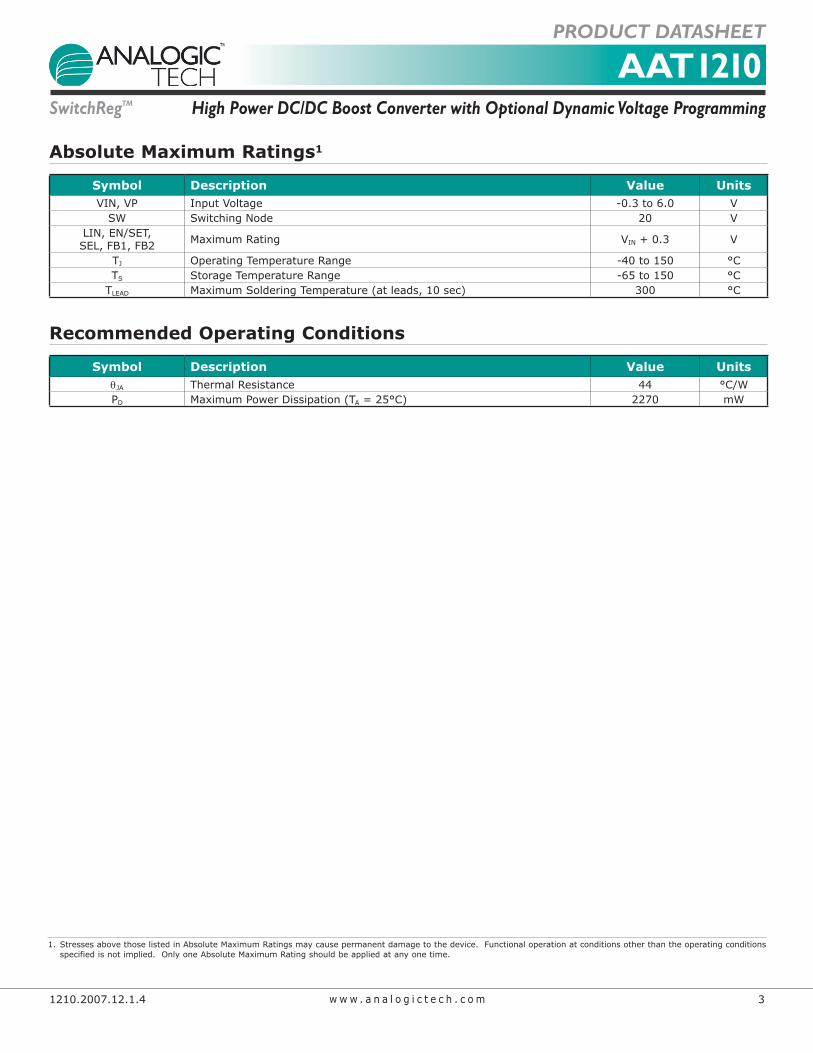
Absolute Maximum Ratings1
Symbol Description Value Units VIN, VP Input Voltage -0.3 to 6.0 V
SW Switching Node 20 V LIN, EN/SET, SEL, FB1, FB2 Maximum Rating VIN + 0.3 V
TJ Operating Temperature Range -40 to 150 °C TS Storage Temperature Range -65 to 150 °C
TLEAD Maximum Soldering Temperature (at leads, 10 sec) 300 °C
Recommended Operating Conditions
Symbol Description Value Units θJA Thermal Resistance 44 °C/WPD Maximum Power Dissipation (TA = 25°C) 2270 mW
1. Stresses above those listed in Absolute Maximum Ratings may cause permanent damage to the device. Functional operation at conditions other than the operating conditions specified is not implied. Only one Absolute Maximum Rating should be applied at any one time.

AAT1210
High Power DC/DC Boost Converter with Optional Dynamic Voltage ProgrammingSwitchRegTM
PRODUCT DATASHEET
4 1210.2007.12.1.4w w w . a n a l o g i c t e c h . c o m
AAT1210
High Power DC/DC Boost Converter with Optional Dynamic Voltage ProgrammingSwitchRegTM
PRODUCT DATASHEET
4 1210.2007.12.1.4w w w . a n a l o g i c t e c h . c o m
Electrical Characteristics1 VIN = 3.6V, TA = -40°C to +85°C, unless otherwise noted. Typical values are TA = 25°C.
Symbol Description Conditions Min Typ Max Units Power Supply
VIN Input Voltage Range 2.7 5.5 V
VOUT Output Voltage Range VIN + 0.5V 18 V
IOUT(MAX) Output Current2
VIN = 2.7V, VOUT = 5V 600mAVIN = 2.7V, VOUT > 5V See note 2
VIN = 3.6V, VOUT > 5V 900
VUVLO UVLO Threshold VIN Rising 2.7 V Hysteresis 150 mV VIN Falling 1.8 V
IQ Quiescent Current SEL = GND, VOUT = 5V, No Load, Switching3 250 μA
SEL = GND, FB2 = 1.5V, Not Switching 40 70 μA ISHDN VIN Pin Shutdown Current EN/SET = GND 1.0 μA
FB1 FB1 Reference Voltage IOUT = 0 to IOUT(MAX) mA, VIN = 2.7V to 5.0V, SEL = High 1.164 1.2 1.236 V
FB2 FB2 Reference Voltage IOUT = 0 to IOUT(MAX) mA, VIN = 2.7V to 5.0V, SEL = Low 0.582 0.6 0.618 V
ΔVLOADREG Load Regulation IOUT = 0 to IOUT(MAX) mA 0.01 %/mA ΔVLINEREG/ΔVIN Line Regulation VIN = 3.0V to 5.5V 0.6 %/V
RDS(ON)L Low Side Switch On Resistance 0.06 Ω
RDS(ON)INInput Disconnect Switch On Resistance 0.18 Ω
TSS Soft-Start Time From Enable to Output Regulation; VOUT = 15V , COUT = 10μF
2.5 ms
TSD Over-Temperature Shutdown Threshold 140 °C
THYS Shutdown Hysteresis 15 °C ILIM N-Channel Current Limit VIN = 3.6V , L =2.2μH 3.0 A
SEL, EN/SETVSEL(L) SEL Threshold Low VIN = 2.7V 0.4 VVSEL(H) SEL Threshold High VIN = 5.5V 1.4 V
VEN/SET(L) Enable Threshold Low VIN = 2.7V 0.4 VVEN/SET(H) Enable Threshold High VIN = 5.5V 1.4 VTEN/SET LO EN/SET Low Time 0.3 75 μs
TEN/SET HI MIN Minimum EN/SET High Time 50 ns TEN/SET HI MAX Maximum EN/SET High Time 75 μs
TOFF EN/SET Off Timeout 500 μs TLAT EN/SET Latch Timeout 500 μs
IEN/SET EN/SET Input Leakage -1 1 μA
1. Specifications over the -40°C to +85°C operating temperature range are assured by design, characterization and correlation with statistical process controls.2. Maximum output power and current is dependent upon operating efficiency and thermal/mechanical design. Output current and output power derating may apply. See Figure 1.3. Total input current with prescribed FB resistor network can be reduced with larger resistor values.
AAT1210
High Power DC/DC Boost Converter with Optional Dynamic Voltage ProgrammingSwitchRegTM
PRODUCT DATASHEET
1210.2007.12.1.4 5w w w . a n a l o g i c t e c h . c o m
AAT1210
High Power DC/DC Boost Converter with Optional Dynamic Voltage ProgrammingSwitchRegTM
PRODUCT DATASHEET
1210.2007.12.1.4 5w w w . a n a l o g i c t e c h . c o m
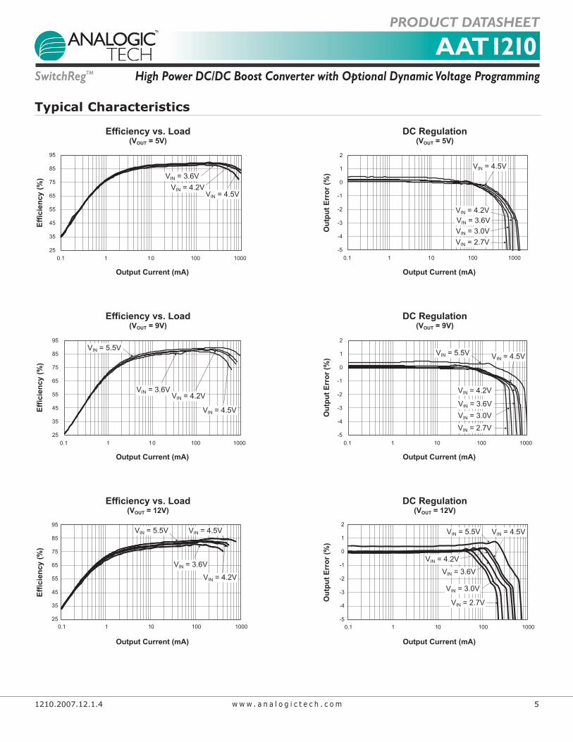
Typical Characteristics
Efficiency vs. Load(VOUT = 5V)
Output Current (mA)
Eff
icie
ncy (
%)
25
35
45
55
65
75
85
95
0.1 1 10 100 1000
VIN = 4.5VVIN = 4.2V
VIN = 3.6V
DC Regulation(VOUT = 5V)
Output Current (mA)
Ou
tpu
t E
rro
r (%
)
-5
-4
-3
-2
-1
0
1
2
0.1 1 10 100 1000
VIN = 4.5V
VIN = 4.2V
VIN = 3.6V
VIN = 3.0V
VIN = 2.7V
Efficiency vs. Load(VOUT = 9V)
Output Current (mA)
Eff
icie
ncy (
%)
25
35
45
55
65
75
85
95
0.1 1 10 100 1000
VIN = 5.5V
VIN = 4.5V
VIN = 4.2VVIN = 3.6V
DC Regulation(VOUT = 9V)
Output Current (mA)
Ou
tpu
t E
rro
r (%
)
-5
-4
-3
-2
-1
0
1
2
0.1 1 10 100 1000
VIN = 5.5VVIN = 4.5V
VIN = 4.2V
VIN = 3.6V
VIN = 3.0V
VIN = 2.7V
Efficiency vs. Load(VOUT = 12V)
Output Current (mA)
Eff
icie
ncy (
%)
25
35
45
55
65
75
85
95
0.1 1 10 100 1000
VIN = 5.5V VIN = 4.5V
VIN = 4.2V
VIN = 3.6V
DC Regulation(VOUT = 12V)
Output Current (mA)
Ou
tpu
t E
rro
r (%
)
-5
-4
-3
-2
-1
0
1
2
0.1 1 10 100 1000
VIN = 5.5V VIN = 4.5V
VIN = 4.2V
VIN = 3.6V
VIN = 3.0V
VIN = 2.7V

AAT1210
High Power DC/DC Boost Converter with Optional Dynamic Voltage ProgrammingSwitchRegTM
PRODUCT DATASHEET
6 1210.2007.12.1.4w w w . a n a l o g i c t e c h . c o m
AAT1210
High Power DC/DC Boost Converter with Optional Dynamic Voltage ProgrammingSwitchRegTM
PRODUCT DATASHEET
6 1210.2007.12.1.4w w w . a n a l o g i c t e c h . c o m
Typical Characteristics
Efficiency vs. Load(VOUT = 15V)
Output Current (mA)
Eff
icie
ncy (
%)
25
35
45
55
65
75
85
95
0.1 1 10 100 1000
VIN = 5.5V VIN = 4.5V
VIN = 4.2V
VIN = 3.6V
DC Regulation(VOUT = 15V)
Output Current (mA)
Ou
tpu
t E
rro
r (%
)
VIN = 4.5V
-5
-4
-3
-2
-1
0
1
2
0.1 1 10 100 1000
VIN = 5.5V
VIN = 4.2V
VIN = 3.6V
VIN = 3.0V
VIN = 2.7V
Line Regulation(VOUT = 12V)
Input Voltage (V)
Accu
racy (
%)
-2
-1.5
-1
-0.5
0
0.5
1
1.5
2
2.5 3 3.5 4 4.5 5 5.5 6
VIN = 2.7V
VIN = 3.0VVIN = 3.6V
VIN = 5.5V
VIN = 4.2V
Output Voltage Error vs. Temperature(VIN = 3.6V; VOUT = 12V; IOUT = 100mA)
Temperature (°°C)
Ou
tpu
t E
rro
r (%
)
-0.5
-0.4
-0.3
-0.2
-0.1
0
0.1
0.2
0.3
0.4
0.5
-40 -15 10 35 60 85
No Load Input Current vs. Input Voltage(EN = High)
Input Voltage (V)
Su
pp
ly C
urr
en
t (m
A)
0
0.5
1
1.5
2
2.5
3
2.5 3 3.5 4 4.5 5 5.5 6
VOUT = 18V
VOUT = 9V
VOUT = 5V
VOUT = 12V
No Load Input Current vs. Temperature(VIN = 3.6V; VOUT = 5V)
Temperature (°°C)
Su
pp
ly C
urr
en
t (m
A)
0.25
0.26
0.27
0.28
0.29
0.3
0.31
0.32
0.33
0.34
-40 -15 10 35 60 85

AAT1210
High Power DC/DC Boost Converter with Optional Dynamic Voltage ProgrammingSwitchRegTM
PRODUCT DATASHEET
1210.2007.12.1.4 7w w w . a n a l o g i c t e c h . c o m
AAT1210
High Power DC/DC Boost Converter with Optional Dynamic Voltage ProgrammingSwitchRegTM
PRODUCT DATASHEET
1210.2007.12.1.4 7w w w . a n a l o g i c t e c h . c o m
Typical Characteristics
AC Output Ripple vs. Output Current(VOUT = 9V)
Output Current (mA)
Ou
tpu
t V
olt
ag
e (
mV
)
0
10
20
30
40
50
60
70
0 50 100 150 200 250 300
VIN = 2.7VVIN = 3.0V
VIN = 3.6V VIN = 4.2V
VIN = 5.5V
Output Ripple(VIN = 3.6V; VOUT = 15V; IOUT = 150mA; L = 1.2µH)
Time (500ns/div)
Ind
ucto
r Cu
rren
t
(bo
ttom
) (A)
Ou
tpu
t V
olt
ag
e
(to
p)
(V)
14.7
14.75
14.8
14.85
14.9
14.95
15
15.05
15.1
-4
-2
0
2
4
6
8
10
12
Output Ripple(VIN = 3.6V; VOUT = 15V; No Load; L = 1.2µH)
Time (200ns/div)
Ind
ucto
r Cu
rren
t
(bo
ttom
) (A)
Ou
tpu
t V
olt
ag
e
(to
p)
(V)
14.7
14.75
14.8
14.85
14.9
14.95
15
15.05
15.1
-0.5
0
0.5
1
1.5
2
2.5
3
3.5
Load Transient Response(VIN = 3.6V; VOUT = 5V; IOUT = 0mA to 600mA)
Time (20µs/div)
Ou
tpu
t Cu
rren
t (A) (m
idd
le)
Ind
ucto
r Cu
rren
t (A) (b
otto
m)
Ou
tpu
t V
olt
ag
e
(to
p)
(V)
3.6
3.8
4
4.2
4.4
4.6
4.8
5
5.2
-1
0
1
2
3
4
5
6
7
0mA
600mA
Load Transient Response(VIN = 3.6V; VOUT = 5V; IOUT = 120mA to 360mA)
Time (20µs/div)
Ou
tpu
t Cu
rren
t (A) (m
idd
le)
Ind
ucto
r Cu
rren
t (A) (b
otto
m)
Ou
tpu
t V
olt
ag
e
(to
p)
(V)
4.65
4.7
4.75
4.8
4.85
4.9
4.95
5
5.05
-1
0
1
2
3
4
5
6
7
120mA
360mA
Load Transient Response(VIN = 3.6V; VOUT = 12V; IOUT = 0mA to 200mA)
Time (20µs/div)
Ou
tpu
t Cu
rren
t (A) (m
idd
le)
Ind
ucto
r Cu
rren
t (A) (b
otto
m)
Ou
tpu
t V
olt
ag
e
(to
p)
(V)
10.8
11
11.2
11.4
11.6
11.8
12
12.2
12.4
-1
0
1
2
3
4
5
6
7
0mA
200mA

AAT1210
High Power DC/DC Boost Converter with Optional Dynamic Voltage ProgrammingSwitchRegTM
PRODUCT DATASHEET
8 1210.2007.12.1.4w w w . a n a l o g i c t e c h . c o m
AAT1210
High Power DC/DC Boost Converter with Optional Dynamic Voltage ProgrammingSwitchRegTM
PRODUCT DATASHEET
8 1210.2007.12.1.4w w w . a n a l o g i c t e c h . c o m
Typical Characteristics
Load Transient Response(VIN = 3.6V; VOUT = 12V; IOUT = 40 to 120mA)
Time (20µs/div)
Ou
tpu
t Cu
rren
t (mid
dle
) (A)
Ind
uc
tor C
urre
nt (b
otto
m) (A
)
Ou
tpu
t V
olt
ag
e
(to
p)
(V)
10.8
11
11.2
11.4
11.6
11.8
12
12.2
12.4
-1
0
1
2
3
4
5
6
7
120mA
40mA
Line Response(VOUT = 15V @ 100mA)
Time (100µs/div)
Inp
ut V
olta
ge
(bo
ttom
) (V)
Ou
tpu
t V
olt
ag
e
(to
p)
(V)
13.5
13.75
14
14.25
14.5
14.75
15
15.25
15.5
2.4
3
3.6
4.2
4.8
5.4
6
6.6
7.2
Line Response(VOUT = 5V @ 100mA)
Time (100µs/div)
Inp
ut V
olta
ge
(bo
ttom
) (V)
Ou
tpu
t V
olt
ag
e
(to
p)
(V)
3.8
4
4.2
4.4
4.6
4.8
5
5.2
5.4
2.4
3
3.6
4.2
4.8
5.4
6
6.6
7.2
P-Channel RDS(ON) vs. Input Voltage
Input Voltage (V)
RD
S(O
N) (m
ΩΩ)
100
120
140
160
180
200
220
240
260
280
300
2.5 3 3.5 4 4.5 5 5.5 6
120°C 100°C
85°C25°C
N-Channel RDS(ON) vs. Input Voltage
Input Voltage (V)
RD
S(O
N) (m
ΩΩ)
40
50
60
70
80
90
100
110
2.5 3 3.5 4 4.5 5 5.5 6
120°C100°C
85°C25°C
Soft Start(VIN = 3.6V; CIN = 2.2µF; IOUT = 100mA; VOUT = 15V)
Time (500µs/div)
Inp
ut C
urre
nt
(bo
ttom
) (A)
En
ab
le V
olt
ag
e (
mid
dle
) (V
)
Ou
tpu
t V
olt
ag
e (
top
) (V
)
-20
-15
-10
-5
0
5
10
15
20
-0.5
0
0.5
1
1.5
2
2.5
3
3.5
1.04V

AAT1210
High Power DC/DC Boost Converter with Optional Dynamic Voltage ProgrammingSwitchRegTM
PRODUCT DATASHEET
1210.2007.12.1.4 9w w w . a n a l o g i c t e c h . c o m
AAT1210
High Power DC/DC Boost Converter with Optional Dynamic Voltage ProgrammingSwitchRegTM
PRODUCT DATASHEET
1210.2007.12.1.4 9w w w . a n a l o g i c t e c h . c o m
Typical Characteristics
Soft Start(VIN = 3.6V; CIN = 2.2µF; IOUT = 100mA; VOUT = 5V)
Time (500µs/div)
Inp
ut C
urre
nt
(bo
ttom
) (A)
Ou
tpu
t V
olt
ag
e (
top
) (V
)
En
ab
le V
olt
ag
e (
mid
dle
) (V
)
-8
-6
-4
-2
0
2
4
6
8
-0.25
0
0.25
0.5
0.75
1
1.25
1.5
1.75
1.04V

AAT1210
High Power DC/DC Boost Converter with Optional Dynamic Voltage ProgrammingSwitchRegTM
PRODUCT DATASHEET
10 1210.2007.12.1.4w w w . a n a l o g i c t e c h . c o m
Functional Description The AAT1210 consists of a DC/DC boost (step-up) con-troller, an integrated slew rate controlled input discon-nect MOSFET switch, and a MOSFET power switch. A high voltage rectifier, power inductor, capacitors and resistor divider network are required to implement a DC/DC boost converter. The minimum output voltage must be 0.5V above the input voltage and the maximum out-put voltage is 18V. The operating input voltage range is 2.7V to 5.5V.
Control Loop
The AAT1210 provides the benefits of current mode con-trol with a simple hysteretic feedback loop. The device maintains exceptional DC regulation, transient response, and cycle-by-cycle current limit without additional com-pensation components.
The AAT1210 modulates the power MOSFET switching current in response to changes in output voltage. This
allows the voltage loop to directly program the required inductor current in response to changes in the output load.
The switching cycle initiates when the N-channel MOSFET is turned ON and current ramps up in the inductor. The ON interval is terminated when the inductor current reaches the programmed peak current level. During the OFF interval, the input current decays until the lower threshold, or zero inductor current, is reached. The lower current is equal to the peak current minus a preset hys-teresis threshold, which determines the inductor ripple current. The peak current is adjusted by the controller until the output current requirement is met.
The magnitude of the feedback error signal determines the average input current. The AAT1210 controller imple-ments a programmed current source connected to the output capacitor and load resistor. There is no right-half plane zero, and loop stability is achieved with no addi-tional compensation components.
Functional Block Diagram
GND
SEL
FB2
FB1
EN/SET
VP LIN
Control
Soft-StartTimer
OutputSelect
VREF1
VREF2
VIN
SW
PGND

AAT1210
High Power DC/DC Boost Converter with Optional Dynamic Voltage ProgrammingSwitchRegTM
PRODUCT DATASHEET
1210.2007.12.1.4 11w w w . a n a l o g i c t e c h . c o m
Increased load current results in a drop in the output feedback voltage (FB1 or FB2) sensed through the feed-back resistors (R1, R2, R3 in Figure 2). The controller responds by increasing the peak inductor current, result-ing in higher average current in the inductor. Alternatively, decreased output load results in an increase in the out-put feedback voltage. The controller responds by decreasing the peak inductor current, resulting in lower average current in the inductor.
At light load, the inductor OFF interval current goes below zero, which terminates the off period, and the boost converter enters discontinuous mode operation. Further reduction in the load results in a corresponding reduction in the switching frequency. The AAT1210 pro-vides optimized light load operation which reduces switching losses and maintains the highest possible effi-ciency at light load.
The AAT1210 switching frequency varies with changes in the input voltage, output voltage, and inductor size. Once the boost converter has reached continuous mode, further increases in the output load will not significantly change the operating frequency and constant ripple cur-rent in the boost inductor is maintained.
Output Voltage Programming
The FB reference voltage is determined by the logic state of the SEL pin. The output voltage is programmed through a resistor divider network (R1, R2, R3) from the positive output terminal to FB1/FB2 pins to ground. Pulling the SEL pin high activates the FB1 pin which maintains a 1.2V reference voltage, while the FB2 refer-ence is disabled. Pulling the SEL pin low activates the FB2 pin which maintains a 0.6V reference, while the FB1 reference is disabled. The FB1 and FB2 pins may be tied together when a static DC output voltage is desired.
Toggling the SEL pin programs the output voltage between two distinct output voltages across a 2.0X range (maximum). With FB1, FB2 tied together, the out-put voltage toggles between two voltages with a 2.0X scaling factor. An additional resistor between FB1 and FB2 pins allows toggling between two voltages with a <2.0X scaling factor.
Alternatively, the output voltage may be dynamically programmed to any of 16 voltage levels using the S2Cwire serial digital input. The single-wire S2Cwire interface provides high-speed output voltage program-
mability across a 2.0X output voltage range. S2Cwire functionality is enabled by pulling the SEL pin low and providing S2Cwire digital clock input to the EN/SET pin which sets the FB2 voltage level from 0.6V to 1.2V. Table 6 details the FB2 reference voltage versus S2Cwire rising clock edges.
Soft Start / Enable
The input disconnect switch is activated when a valid input voltage is present and the EN/SET pin is pulled high. The slew rate control on the P-channel MOSFET ensures minimal inrush current as the output voltage is charged to the input voltage, prior to switching of the N-channel power MOSFET. Monotonic turn-on is guaran-teed by the integrated soft-start circuitry.
Soft-start time of approximately 2.5ms is internally pro-grammed to minimize inrush current and eliminate out-put voltage overshoot across the full input voltage range under all loading conditions.
Some applications may require the output to be active when a valid input voltage is present. In these cases, add a 10kΩ resistor between the VIN, VP, and EN/SET pins to avoid startup issues.
Current Limit and Over-Temperature Protection
The switching of the N-channel MOSFET terminates if the current limit of 3.0A (minimum) is exceeded. This minimizes power dissipation and component stresses under overload and short-circuit conditions. Switching resumes when the current decays below the current limit.
Thermal protection disables the AAT1210 if internal power dissipation becomes excessive. Thermal protec-tion disables both the N-channel and P-channel MOSFETs. The junction over-temperature threshold is 140°C with 15°C of hysteresis. The output voltage automatically recovers when the over-temperature or over-current fault condition is removed.
Under-Voltage Lockout
Internal bias of all circuits is controlled via the VIN input. Under-voltage lockout (UVLO) guarantees sufficient VIN bias and proper operation of all internal circuitry prior to activation.

AAT1210
High Power DC/DC Boost Converter with Optional Dynamic Voltage ProgrammingSwitchRegTM
PRODUCT DATASHEET
12 1210.2007.12.1.4w w w . a n a l o g i c t e c h . c o m
Applications Information
Output Current and Power Capability
The AAT1210 boost converter provides a high voltage, high current, regulated DC output voltage from a low voltage DC input. The operating input voltage range is 2.7 to 5.5V.
Figure 1 details the output current and power capability of the AAT1210 for output voltages from 5V to 18V with DC input of 2.7V, 3.6V and 4.5V. The maximum output current/power curves are based on +50°C case tem-perature rise over ambient using the TDFN34-16 pack-age. Ambient temperature at 25°C, natural convection is assumed. Up to 1.3A of output current is possible with 4.5V input voltage. As shown in Figure 1, the output capability is somewhat reduced at higher output voltage and reduced input voltage.
The AAT1210 schematic and PCB layout are provided in Figures 2, 6, and 7. The PCB layout includes a small 1 ounce copper power plane on top and bottom layers which is tied to the paddle of the TDFN34-16 package. The top plane is soldered directly to the paddle, and tied to the bottom layer with plated through vias. Details of the PCB layout are provided in Figures 6, 7, and 8.
Actual case temperature may vary and depends on the boost converter efficiency and the system thermal design; including, but not limited to airflow, local heat sources, etc. Additional derating may apply.
Selecting the Output Diode
To ensure minimum forward voltage drop and no recov-ery, a high voltage Schottky diode is considered the best choice for use with the AAT1210 boost converter. The AAT1210 output diode is sized to maintain acceptable efficiency and reasonable operating junction tempera-ture under full load operating conditions. Forward volt-age (VF) and package thermal resistance (θJA) are the dominant factors to consider in selecting a diode. The diode’s published current rating may not reflect actual operating conditions and should be used only as a com-parative measure between similarly rated devices. 20V rated Schottky diodes are recommended for outputs less than 15V, while 30V rated Schottky diodes are recom-mended for outputs greater than 15V.
The switching period is divided between ON and OFF time intervals.
= TON + TOFF
1
FS
AAT1210 Boost Converter Maximum Output Capability
Output Voltage (V)
Ma
xim
um
Ou
tpu
t C
urr
en
t (m
A) M
ax
imu
m O
utp
ut P
ow
er (W
)
0
200
400
600
800
1000
1200
1400
5 6 7 8 9 10 11 12 13 14 15 16 17 18
0
1
2
3
4
5
6
7
VIN = 4.5V
VIN = 3.6V
Output Current
Output Power
VIN = 2.7V
Figure 1: Maximum Output Power Vs. Output Voltage for TC(RISE) = +50ºC(assumes TDFN34-16 paddle heatsinking; see Figures 6, 7, and 8).

AAT1210
High Power DC/DC Boost Converter with Optional Dynamic Voltage ProgrammingSwitchRegTM
PRODUCT DATASHEET
1210.2007.12.1.4 13w w w . a n a l o g i c t e c h . c o m
During the ON time, the N-channel power MOSFET is conducting and storing energy in the boost inductor. During the OFF time, the N-channel power MOSFET is not conducting. Stored energy is transferred from the input supply and boost inductor to the output load through the output diode. Duty cycle is defined as the ON time divided by the total switching interval.
TON
TON + TOFF
D =
= TON ⋅ FS
The maximum duty cycle can be estimated from the relationship for a continuous mode boost converter. Maximum duty cycle (DMAX) is the duty cycle at minimum input voltage (VIN(MIN)).
VOUT - VIN(MIN)
VOUT
DMAX =
The average diode current during the OFF time can be estimated.
IOUT
1 - DMAX
IAVG(OFF) =
The following curves show the VF characteristics for dif-ferent Schottky diodes (100°C case). The VF of the Schottky diode can be estimated from the average cur-rent during the off time.
Forward Voltage (V)
Fo
rward
Cu
rren
t (m
A)
10
100
1000
10000
0.00 0.10 0.20 0.30 0.40 0.50 0.60 0.70
B340LA
MBR0530
ZHCS350
BAT42W
Figure 3: Forward Voltage vs. Forward Current for Various Schottky Diodes.
The average diode current is equal to the output current.
IAVG(TOT) = IOUT
D1 Schottky
123
Enable
JP1
123
Select
JP24.7μF
C1
U1 AAT1210 TDFN34-16C1 6.3V 0603 4.7μFC2 10V 0805 10μFD1 30V 0.5A MBR0530T1 SOD-123L1 0.47μH SD10-R47-RR1 36.5k 0603R2 549 0603R3 4.99k 0603R4 10k 0603
VP 16
VP 15
EN/SET 14
SEL 13
PGND8 PGND7 PGND6 GND5 FB24 FB13 LIN2 LIN1
VIN 12
N/C 11
SW 10
SW 9
AAT1210_TDFN34-16
U1VIN: 2.7V to 5.5V
C210μF10V
R2549
R136.5k
R34.99k
9V at 300mA5V at 600mA
L10.47μH
R4
10K
Figure 2: AAT1210 Demo Board Schematic.

AAT1210
High Power DC/DC Boost Converter with Optional Dynamic Voltage ProgrammingSwitchRegTM
PRODUCT DATASHEET
14 1210.2007.12.1.4w w w . a n a l o g i c t e c h . c o m
The average output current multiplied by the forward diode voltage determines the loss of the output diode.
PLOSS_DIODE = IAVG · VF
= IOUT · VF
Diode junction temperature can be estimated.
TJ = TAMB + ΘJA · PLOSS_DIODE
The junction temperature should be maintained below 110ºC, but may vary depending on application and/or system guidelines. The diode θJA can be minimized with additional PCB area on the cathode. PCB heatsinking the anode may degrade EMI performance.
The reverse leakage current of the rectifier must be con-sidered to maintain low quiescent (input) current and high efficiency under light load. The rectifier reverse cur-rent increases dramatically at high temperatures.
Additional considerations may apply to satisfy short cir-cuit conditions. A short circuit across the output termi-nals results in high currents through the inductor and output diode. The output diode must be sized to prevent damage and possible failure of the diode under short circuit conditions. The inductor may saturate without incurring damage.
When current limit of (3A minimum) is reached, switch-ing of the low side N-channel MOSFET is disabled. Although switching is disabled, DC current continues to build to a level determined by the DC resistance in the path of current flow. For portable applications, the source resistance (RSOURCE) of the Li-ion battery pack is between 100-300mΩ and should also be considered.
ISHT-CKT(MAX) =(VIN(MAX) - VF)
(RSOURCE + RDC + RDS(ON)IN)
The AAT1210 controller will generate an over-tempera-ture (OT) event under extended short circuit conditions. OT disables the high side P-channel MOSFET, which ter-minates current flow in the output diode. Current flow continues when OT hysteresis (cool-down) is met. This continues until the short circuit condition is removed. In portable applications, the battery pack over-current pro-tection may be enabled prior to an OT event.
The diode non-repetitive peak surge current (IFSM) rating should be greater than ISHT_CKT(MAX) to ensure diode reli-ability under short circuit conditions. Typically, IFSM cur-rent is specified for conduction periods from 8-10ms. If short circuit survivability is required, it is recommended to verify ISHT_CKT(MAX) under actual operating conditions across the expected operating temperature range.
Selecting the Boost Inductor
The AAT1210 controller utilizes hysteretic control and the switching frequency varies with output load and input voltage. The value of the inductor determines the maximum switching frequency of the boost converter. Increased output inductance decreases the switching frequency, resulting in higher peak currents and increased output voltage ripple. The required inductance increases with increasing output voltage. The inductor is sized from 0.47μH to 2.2μH for output voltages from 5V to 18V. This selection maintains high frequency switching (up to 2MHz), low output ripple and minimum solution size. A summary of recommended inductors and capaci-tors for 5V to 18V fixed outputs is provided in Table 2.
The physical size of the inductor may be reduced when operating at greater than 2.7V input voltage and/or less than maximum rated output power is desired (see Figure 1 for maximum output power estimate). Figure 4 pro-vides the peak inductor current (IPEAK) versus output power for different input voltage levels. The curves are valid for all output voltages and assume the correspond-ing inductance value provided in Figure 4. The inductor is selected to maintain IPEAK current less than the speci-fied saturation current (ISAT).
Output Power (W)
Peak In
du
cto
r C
urr
en
t (m
A)
0
500
1000
1500
2000
2500
3000
3500
0.0 1.0 2.0 3.0 4.0 5.0 6.0 7.0
VIN = 4.5V
VIN = 3.6VVIN = 2.7V
Figure 4: Peak Inductor Current (IPEAK)vs. Output Power.

AAT1210
High Power DC/DC Boost Converter with Optional Dynamic Voltage ProgrammingSwitchRegTM
PRODUCT DATASHEET
1210.2007.12.1.4 15w w w . a n a l o g i c t e c h . c o m
The RMS current flowing through the boost inductor is equal to the DC plus AC ripple components. Under worst-case RMS conditions, the current waveform is critically continuous. The resulting RMS calculation yields worst-case inductor loss. The RMS value should be com-pared against the manufacturer’s temperature rise, or thermal derating, guidelines.
IPEAK IRMS =
3
In most cases, the inductor’s specified IRMS current will be greater than the IRMS current required by the boost inductor.
For a given inductor type, smaller inductor size leads to an increase in DCR winding resistance and, in most cases, increased thermal impedance. Winding resistance degrades boost converter efficiency and increases the inductor operating temperature.
PLOSS_INDUCTOR = IRMS2 · DCR
To ensure high reliability, the inductor temperature should not exceed 100°C. Manufacturer’s recommenda-tions should be consulted. In some cases, PCB heatsink-ing applied to the AAT1210 LIN node (non-switching) can improve the inductor’s thermal capability. PCB heat-sinking may degrade EMI performance when applied to the SW node (switching) of the AAT1210.
Shielded inductors provide decreased EMI and may be required in noise sensitive applications. Unshielded chip inductors provide significant space savings at a reduced cost compared to shielded (wound and gapped) induc-tors. Chip-type inductors have increased winding resis-tance when compared to shielded, wound varieties.
Selecting DC/DC Boost Capacitors
Recommended input and output capacitors for output voltages from 5V to 18V are provided in Table 4.
The high output ripple inherent in the boost converter necessitates low impedance output filtering. Multi-layer ceramic (MLC) capacitors provide small size and high capacitance, low parasitic equivalent series resistance (ESR) and equivalent series inductance (ESL), and are well suited for use with the AAT1210 boost regulator. MLC capacitors of type X7R or X5R are recommended to ensure good capacitance stability over the full operating temperature range.
The output capacitor is sized to maintain the output load without significant voltage droop (ΔVOUT) during the power switch ON interval, when the output diode is not conducting. A ceramic output capacitor from 4.7μF to 10μF is recommended. Output capacitors should be rated from 10V to 25V, depending on the maximum desired output voltage. Ceramic capacitors sized as small as 0603 are available which meet these requirements.
Manufacturer Part Number Rated Forward
Current (A)
Non-Repetitive Peak Surge Current (A)
Rated Voltage (V)
Thermal Resistance (θJA, °C/W) Case
Diodes, Inc. BAT42W 0.2 4.0 30 500 SOD-123ON Semi MBR0530T 0.5 5.5 30 206 SOD-123
Zetex ZHCS350 0.35 4.2 40 330 SOD-523Central Semi CMDSH2-3 0.2 1.0 30 500 SOD-323
Table 1: Typical Surface Mount Schottky Rectifiers for Various Output Levels.
VOUT C1 (Input Capacitor) C2 (Output Capacitor) L1 (Boost Inductor)5.0 4.7μF 10μF/6.3V, 10V 0.47μH9.0 4.7μF 10μF/10V 0.47μH12.0 4.7μF 10μF/16V 1.0/1.2μH15.0 4.7μF 10μF/16V 1.0/1.2μH18.0 4.7μF 4.7μF/25V 2.2μH
Table 2: Output Inductor and Capacitor Values Vs. Output Voltage

AAT1210
High Power DC/DC Boost Converter with Optional Dynamic Voltage ProgrammingSwitchRegTM
PRODUCT DATASHEET
16 1210.2007.12.1.4w w w . a n a l o g i c t e c h . c o m
Manufacturer Part NumberInductance
(μH)
MaxDC ISAT Current
(A)
Max IRMS
Current(A)
DCR (mΩ)
SizeLxWxH (mm) Type
Sumidawww.sumida.com
CDRH5D16-1R4 1.4 4.7 4.7 14.6 5.8x5.8x1.8 ShieldedCDRH5D16-1R4 2.2 3.0 2.85 35.9 5.8x5.8x1.8 Shielded
CDRH3D11/HP-1R5 1.5 2.0 1.45 80 4.0x4.0x1.2 ShieldedCDRH3D11/HP-2R7 2.7 1.55 1.3 100 4.0x4.0x1.2 Shielded
Muratawww.murata.com
LQH55DNR47M03 0.47 4.8 - 13 5.7x5.0x4.7 Non-ShieldedLQH55DN1R0M03 1.0 4.0 - 19 5.7x5.0x4.7 Non-ShieldedLQH55DN1R5M03 1.5 3.7 - 22 5.7x5.0x4.7 Non-ShieldedLQH55DN2R2M03 2.2 3.2 - 29 5.7x5.0x4.7 Non-Shielded
Cooperwww.cooperet.com
SD3814-R47 0.47 4.44 2.81 20 4.0x4.0x1.4 ShieldedSD3814-1R2 1.2 2.67 1.85 46 4.0x4.0x1.4 ShieldedSD3814-2R2 2.2 1.9 1.43 77 4.0x4.0x1.4 ShieldedSD10-R47-R 0.47 3.54 2.59 24.9 5.2x5.2x1.0 ShieldedSD10-1R0-R 1 2.25 1.93 44.8 5.2x5.2x1.0 ShieldedSD10-2R2-R 2.2 1.65 1.35 91.2 5.2x5.2x1.0 ShieldedSD18-2R2-R 2.2 2.16 2.55 39.8 5.2x5.2x1.8 Shielded
Table 3: Recommended Inductors.
Manufacturer Part Number Value (μF)Voltage
Rating (V)Temp.
Co. Case Size
Muratawww.murata.com
GRM188R60J475KEAD 4.7 6.3 X5R 0603GRM21BR61A475KA73L 4.7 10 X5R 0805GRM21BR61E475KA12L 4.7 25 X5R 0805GRM188R60J106ME47D 10 6.3 X5R 0603GRM21BR61A106KE19L 10 10 X5R 0805GRM219R61A106KE44D 10 10 X5R 0805 (H = 0.85mm)GRM21BR61C106KE15L 10 16 X5R 0805
Table 4: Recommended MLC Capacitors.
Minimum 6.3V rated ceramic capacitors are required at the input. Ceramic capacitors sized as small as 0603 are available which meet these requirements. Output capac-itors should be rated from 6.3V to 25V, depending on the maximum desired output voltage.
MLC capacitors exhibit significant capacitance reduction with applied voltage. Output ripple measurements should confirm that output voltage droop and converter stability is acceptable. Voltage derating can minimize this factor, but results may vary with package size and among spe-cific manufacturers.
Output capacitor size can be estimated at a switching frequency (FSW) of 500kHz (worst-case).
IOUT · DMAX
FS · ΔVOUT
COUT =
The boost converter input current flows during both ON and OFF switching intervals. The input ripple current is less than the output ripple and, as a result, less input capacitance is required. A ceramic output capacitor from 4.7μF to 10μF is recommended. The voltage rating of the capacitor must be greater than, or equal to, the maximum operating output voltage. X5R ceramic capac-itors are available in 6.3V, 10V, 16V and 25V rating. Ceramic capacitors sized as small as 0603 are available which meet these requirements.

AAT1210
High Power DC/DC Boost Converter with Optional Dynamic Voltage ProgrammingSwitchRegTM
PRODUCT DATASHEET
1210.2007.12.1.4 17w w w . a n a l o g i c t e c h . c o m
Minimum 6.3V rated ceramic capacitors are required at the input. Ceramic capacitors sized as small as 0603 are available which meet these requirements.
Setting the Output Voltage
The minimum output voltage must be greater than the specified maximum input voltage plus 0.5V margin to maintain proper operation of the AAT1210 boost con-verter. The output voltage may be programmed through a resistor divider network located from the output to FB1 and FB2 pins to ground. Pulling the SEL pin high acti-vates the FB1 pin which maintains a 1.2V reference volt-age, while the FB2 reference is disabled. Pulling the SEL pin low activates the FB2 pin which maintains a 0.6V reference, while the FB1 reference is disabled.
The AAT1210 output voltage can be programmed by one of three methods. First, the output voltage can be static by pulling the SEL logic pin either high or low. Second, the output voltage can be dynamically adjusted between two pre-set levels within a 2X operating range by tog-gling the SEL logic pin. Third, the output can be dynam-ically adjusted to any of 16 preset levels within a 2X operating range using the integrated S2Cwire single wire interface via the EN/SET pin. See Table 5 for static and dynamic output voltage settings.
Table 5 provides details of resistor values for common output voltages from 5V to 18V for SEL = High and SEL = Low options. SEL = High corresponds to VOUT(1) and SEL = Low corresponds to VOUT(2).
Option 1: Static Output Voltage Most DC/DC boost converter applications require a static (fixed) output voltage. If a static voltage is desired, the FB1 pin should be connected directly to FB2 and a resistor between FB1 and FB2 pins is not required.
A static output voltage can be configured by pulling the SEL either high or low. SEL pin high activates the FB1 reference pin to 1.2V (nominal). Alternatively, the SEL
pin is pulled low to activate the FB2 reference at 0.6V (nominal). Table 5 provides details of resistor values for common output voltages from 5V to 18V for SEL = High and SEL = Low options.
Option 2: Dynamic Voltage Control Using SEL Pin The output may be dynamically adjusted between two output voltages by toggling the SEL logic pin. Output voltages VOUT(1) and VOUT(2) correspond to the two output references, FB1 and FB2. Pulling the SEL logic pin high activates VOUT(1), while pulling the SEL logic pin low acti-vates VOUT(2).
In addition, the ratio of output voltages VOUT(2)/VOUT(1) is always less than 2.0, corresponding to a 2X (maximum) programmable range.
Option 3: Dynamic Voltage Control Using S2Cwire Interface The output can be dynamically adjusted by the host controller to any of 16 pre-set output voltage levels using the integrated S2Cwire interface. The EN/SET pin serves as the S2Cwire interface input. The SEL pin must be pulled low when using the S2Cwire interface.
S2Cwire Serial Interface
AnalogicTech’s S2Cwire serial interface is a proprietary high-speed single-wire interface. The S2Cwire interface records rising edges of the EN/SET input and decodes into 16 different states. Each state corresponds to a voltage setting on the FB2 pin, as shown in Table 6.
S2Cwire Output Voltage Programming
The AAT1210 is programmed through the S2Cwire inter-face according to Table 6. The rising clock edges received through the EN/SET pin determine the feedback refer-ence and output voltage set-point. Upon power-up with the SEL pin low and prior to S2Cwire programming, the default feedback reference voltage is set to 0.6V.

AAT1210
High Power DC/DC Boost Converter with Optional Dynamic Voltage ProgrammingSwitchRegTM
PRODUCT DATASHEET
18 1210.2007.12.1.4w w w . a n a l o g i c t e c h . c o m
VOUT(1)
(SEL = High)VOUT(2)
(SEL = Low)
R3 = 4.99kΩ
R1 (kΩ) R2 (kΩ)5.0V - 15.8 06.0V - 20.0 07.0V - 24.3 08.0V - 28.0 09.0V - 32.4 010.0V - 36.5 0 12.0V - 44.2 0 15.0V - 57.6 0 16.0V - 61.9 0 18.0V - 69.8 0
- 5.0V 36.5 0- 6.0V 45.3 0- 7.0V 53.6 0- 8.0V 61.9 0- 9.0V 69.8 0- 10.0V 78.7 0 - 12.0V 95.3 0 - 15.0V 121 0 - 16.0V 127 0 - 18.0V 143 0
9.0V 5.0V 36.5 0.54910.0V 9.0V 66.5 4.0212.0V 10.0V 75 3.32 15.0V 10.0V 76.8 1.65 15.0V 12.0V 90.9 3.0116.0V 10.0V 76.8 1.24 18.0V 10.0V 78.7 0.562 15.0V 12.0V 90.9 3.01 16.0V 12.0V 93.1 2.49 18.0V 12.0V 93.1 1.65 18.0V 15.0V 115 3.32
Table 5: SEL Pin Voltage Control Resistor Values (1% resistor tolerance).
EN/SETRising Edges
FB2 Reference
Voltage (V)
EN/SETRising Edges
FB2 Reference
Voltage (V)1 0.60 (Default) 9 0.922 0.64 10 0.963 0.68 11 1.004 0.72 12 1.045 0.76 13 1.086 0.80 14 1.127 0.84 15 1.168 0.88 16 1.20
Table 6: S2Cwire Voltage Control Settings (SEL = Low).
S2Cwire Serial Interface Timing
The S2Cwire serial interface has flexible timing. Data can be clocked-in at speeds up to 1MHz. After data has been submitted, EN/SET is held high to latch the data for a period TLAT. The output is subsequently changed to the predetermined voltage. When EN/SET is set low for a time greater than TOFF, the AAT1210 is disabled. When disabled, the register is reset to the default value, which sets the FB2 pin to 0.6V if EN is subsequently pulled high.
PCB Layout
Boost converter performance can be adversely affected by poor layout. Possible impact includes high input and out-put voltage ripple, poor EMI performance, and reduced operating efficiency. Every attempt should be made to optimize the layout in order to minimize parasitic PCB effects (stray resistance, capacitance, inductance) and EMI coupling from the high frequency SW node.
A suggested PCB layout for the AAT1210 boost converter is shown in Figures 6, 7, and 8. The following PCB layout guidelines should be considered:
1. Minimize the distance from Capacitor C1 and C2 nega-tive terminal to the PGND pins. This is especially true with output capacitor C2, which conducts high ripple current from the output diode back to the PGND pins.
2. Place the feedback resistors close to the output termi-nals. Route the output pin directly to resistor R1 to maintain good output regulation. R3 should be rout-ed close to the output GND pin, but should not share a significant return path with output capacitor C2.
3. Minimize the distance between L1 to D1 and switch-ing pin SW; minimize the size of the PCB area con-nected to the SW pin.
4. Maintain a ground plane and connect to the IC PGND pin(s) as well as the GND terminals of C1 and C2.
5. Consider additional PCB area on D1 cathode to maximize heatsinking capability. This may be neces-sary when using a diode with a high VF and/or ther-mal resistance.
6. To maximize thermal capacity, connect the exposed paddle to the top and bottom power planes using plated through vias. Top and bottom planes should not extend far beyond the TDFN34-16 package boundary to minimize stray EMI.
7. To avoid problems at startup, add a 10kΩ resistor between the VIN, VP and EN/SET pins (R4). This is critical in applications requiring immunity from input noise during “hot plug” events, e.g. when plugged into an active USB port.

AAT1210
High Power DC/DC Boost Converter with Optional Dynamic Voltage ProgrammingSwitchRegTM
PRODUCT DATASHEET
1210.2007.12.1.4 19w w w . a n a l o g i c t e c h . c o m
1
EN/SET2 n-1 n ≤ 16
Data Reg 0 n-1 0
THI
TLO TLAT TOFF
Figure 5: S2Cwire Timing Diagram.
Figure 6: AAT1210 Evaluation Board Figure 7: AAT1210 Evaluation Board Top Side Layout. Bottom Side Layout.
Figure 8: Exploded View of AAT1210 Evaluation Board Top Side Layout Detailing Plated Through Vias.

AAT1210
High Power DC/DC Boost Converter with Optional Dynamic Voltage ProgrammingSwitchRegTM
PRODUCT DATASHEET
20 1210.2007.12.1.4w w w . a n a l o g i c t e c h . c o m
AAT1210
High Power DC/DC Boost Converter with Optional Dynamic Voltage ProgrammingSwitchRegTM
PRODUCT DATASHEET
20 1210.2007.12.1.4w w w . a n a l o g i c t e c h . c o m
Ordering Information
Package Marking1 Part Number (Tape and Reel)2
TDFN34-16 VDXYY AAT1210IRN-0.6-T1
All AnalogicTech products are offered in Pb-free packaging. The term “Pb-free” means semiconductor products that are in compliance with current RoHS standards, including the requirement that lead not exceed 0.1% by weight in homogeneous materials. For more information, please visit our website at http://www.analogictech.com/about/quality.aspx.
Package Information3
TDFN34-16
3.000 ± 0.050 1.600 ± 0.050
0.050 ± 0.050 0.229 ± 0.051
(4x)
0.85
0 M
AX
4.00
0 ±
0.05
0
3.30
0 ±
0.05
0
Index AreaDetail "A"
Top View Bottom View
Side View
0.350 ± 0.100
0.23
0 ±
0.05
00.
450
± 0.
050
Detail "A"
Pin 1 Indicator(optional)
C0.3
All dimensions in millimeters.
1. XYY = assembly and date code.2. Sample stock is generally held on part numbers listed in BOLD.3. The leadless package family, which includes QFN, TQFN, DFN, TDFN and STDFN, has exposed copper (unplated) at the end of the lead terminals due to the manufacturing
process. A solder fillet at the exposed copper edge cannot be guaranteed and is not required to ensure a proper bottom solder connection.

AAT1210
High Power DC/DC Boost Converter with Optional Dynamic Voltage ProgrammingSwitchRegTM
PRODUCT DATASHEET
1210.2007.12.1.4 21w w w . a n a l o g i c t e c h . c o m
AAT1210
High Power DC/DC Boost Converter with Optional Dynamic Voltage ProgrammingSwitchRegTM
PRODUCT DATASHEET
1210.2007.12.1.4 21w w w . a n a l o g i c t e c h . c o m
Advanced Analogic Technologies, Inc.3230 Scott Boulevard, Santa Clara, CA 95054Phone (408) 737-4600Fax (408) 737-4611
© Advanced Analogic Technologies, Inc.AnalogicTech cannot assume responsibility for use of any circuitry other than circuitry entirely embodied in an AnalogicTech product. No circuit patent licenses, copyrights, mask work rights, or other intellectual property rights are implied. AnalogicTech reserves the right to make changes to their products or specifi cations or to discontinue any product or service without notice. Except as provided in AnalogicTech’s terms and conditions of sale, AnalogicTech assumes no liability whatsoever, and AnalogicTech disclaims any express or implied warranty relating to the sale and/or use of AnalogicTech products including liability or warranties relating to fi tness for a particular purpose, merchantability, or infringement of any patent, copyright or other intellectual property right. In order to minimize risks associated with the customer’s applications, adequate design and operating safeguards must be provided by the customer to minimize inherent or procedural hazards. Testing and other quality control techniques are utilized to the extent AnalogicTech deems necessary to support this warranty. Specifi c testing of all parameters of each device is not necessarily performed. AnalogicTech and the AnalogicTech logo are trademarks of Advanced Analogic Technologies Incorporated. All other brand and product names appearing in this document are registered trademarks or trademarks of their respective holders.