Embed Size (px)
Citation preview
Switched Capacitor DC-DC Converter: Superior where
the Buck Converter has Dominated
Vincent Wai-Shan NgSeth R. Sanders
Electrical Engineering and Computer SciencesUniversity of California at Berkeley
Technical Report No. UCB/EECS-2011-94
http://www.eecs.berkeley.edu/Pubs/TechRpts/2011/EECS-2011-94.html
August 17, 2011

Copyright © 2011, by the author(s).All rights reserved.
Permission to make digital or hard copies of all or part of this work forpersonal or classroom use is granted without fee provided that copies arenot made or distributed for profit or commercial advantage and that copiesbear this notice and the full citation on the first page. To copy otherwise, torepublish, to post on servers or to redistribute to lists, requires prior specificpermission.
Acknowledgement
I would like to thank my adviser, Professor Seth Sanders, for his guidanceand support throughout my years of graduate studies. I would also like tothank my committee members, Professor Elad Alon, and Professor RobertoHorowitz for their advice on my thesis and research. I must also thank myfellow colleagues, Jason Stauth, Hanh-Phuc Le, Mervin John and MichaelSeeman for their help throughout my studies. Last but not least, I mustthankmy parents, my family and my dear friends. Doing a PhD here and goingthrough all the exams and hurdles are definitely not easy, and I amsincerely thankful to have all of you bymy side. I devote this thesis to all of you, and wish you good luck in all your

endeavors.
Switched Capacitor DC-DC Converter:
Superior where the Buck Converter has Dominated
By
Vincent Wai-Shan Ng
A dissertation submitted in partial satisfaction of the
requirements for the degree of
Doctor of Philosophy
in
Engineering – Electrical Engineering and Computer Sciences
in the
Graduate Division
of the
University of California, Berkeley
Committee in charge:
Professor Seth Sanders, Chair Professor Elad Alon
Professor Roberto Horowitz
Fall 2011

1
Abstract
Switched Capacitor DC-DC Converter: Superior where the Buck Converter has Dominated
By
Vincent Wai-Shan Ng
Doctor of Philosophy in Engineering - Electrical Engineering and Computer Science
University of California, Berkeley
Professor Seth R. Sanders, Chair
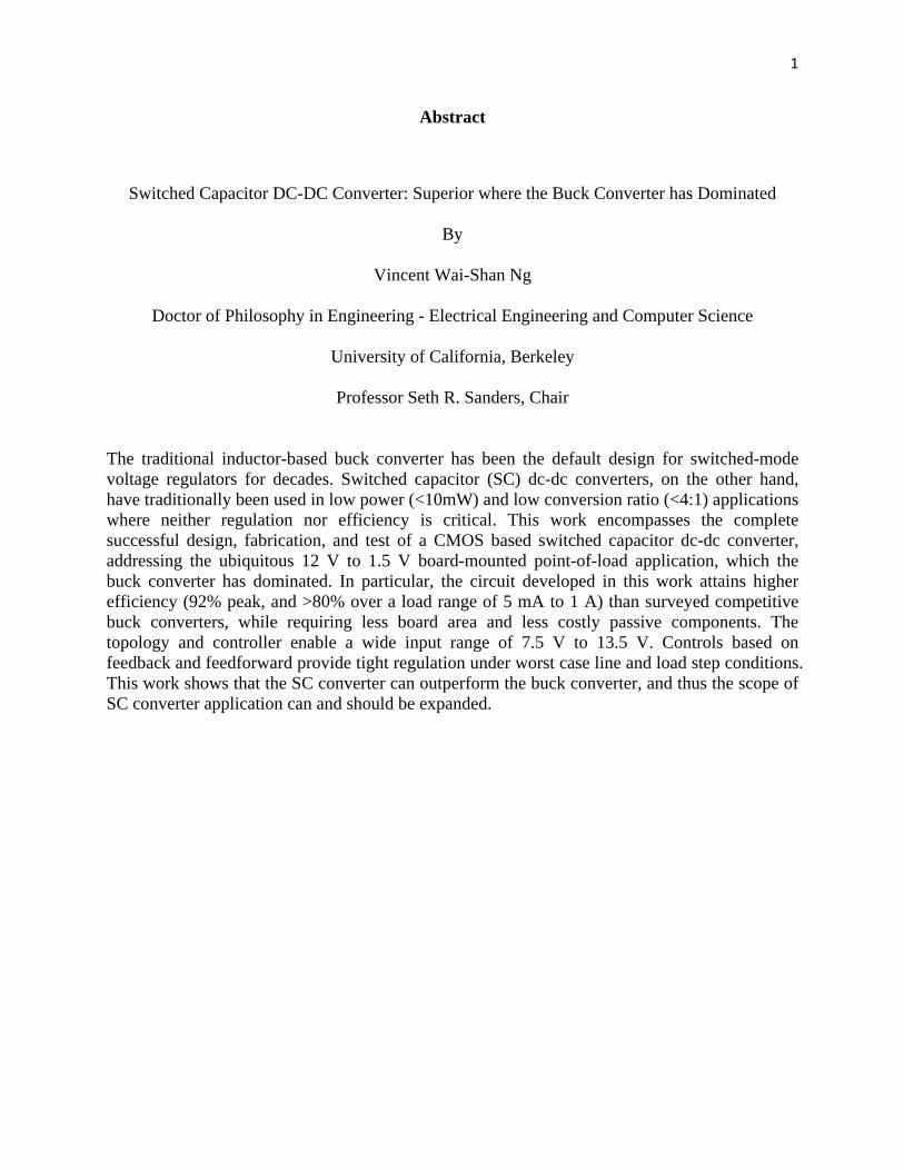
The traditional inductor-based buck converter has been the default design for switched-mode voltage regulators for decades. Switched capacitor (SC) dc-dc converters, on the other hand, have traditionally been used in low power (<10mW) and low conversion ratio (<4:1) applications where neither regulation nor efficiency is critical. This work encompasses the complete successful design, fabrication, and test of a CMOS based switched capacitor dc-dc converter, addressing the ubiquitous 12 V to 1.5 V board-mounted point-of-load application, which the buck converter has dominated. In particular, the circuit developed in this work attains higher efficiency (92% peak, and >80% over a load range of 5 mA to 1 A) than surveyed competitive buck converters, while requiring less board area and less costly passive components. The topology and controller enable a wide input range of 7.5 V to 13.5 V. Controls based on feedback and feedforward provide tight regulation under worst case line and load step conditions. This work shows that the SC converter can outperform the buck converter, and thus the scope of SC converter application can and should be expanded.
CONTENTS i
Contents
0 Executive Summary 1
1 Introduction 8
1.1 The model used for SC converter . . . . . . . . . . . . . . . . . . . . . . . . 91.1.1 SSL model of SC Converter . . . . . . . . . . . . . . . . . . . . . . . 91.1.2 FSL model of SC Converter . . . . . . . . . . . . . . . . . . . . . . . 111.1.3 Combined model of SC Converter . . . . . . . . . . . . . . . . . . . . 12
1.2 Advantages of SC converters . . . . . . . . . . . . . . . . . . . . . . . . . . . 131.2.1 Active element analysis . . . . . . . . . . . . . . . . . . . . . . . . . . 131.2.2 Passive element analysis . . . . . . . . . . . . . . . . . . . . . . . . . 151.2.3 Switching loss analysis . . . . . . . . . . . . . . . . . . . . . . . . . . 16
1.3 Target applications of this work . . . . . . . . . . . . . . . . . . . . . . . . . 17
2 Architecture 19
2.1 Topology choice . . . . . . . . . . . . . . . . . . . . . . . . . . . . . . . . . . 192.2 Multiple voltage domains . . . . . . . . . . . . . . . . . . . . . . . . . . . . . 212.3 Device sizing and optimization . . . . . . . . . . . . . . . . . . . . . . . . . . 23
2.3.1 Capacitor Sizing . . . . . . . . . . . . . . . . . . . . . . . . . . . . . 232.3.2 Switch sizing . . . . . . . . . . . . . . . . . . . . . . . . . . . . . . . 252.3.3 Overall optimization . . . . . . . . . . . . . . . . . . . . . . . . . . . 25
2.4 Multi-conversion-ratio design . . . . . . . . . . . . . . . . . . . . . . . . . . . 282.4.1 Integer step topology . . . . . . . . . . . . . . . . . . . . . . . . . . . 282.4.2 Half step topology . . . . . . . . . . . . . . . . . . . . . . . . . . . . 29
2.5 Shutdown and Startup . . . . . . . . . . . . . . . . . . . . . . . . . . . . . . 322.5.1 Shutdown protection . . . . . . . . . . . . . . . . . . . . . . . . . . . 322.5.2 Startup scheme . . . . . . . . . . . . . . . . . . . . . . . . . . . . . . 32
3 Regulation 34
3.1 Possible control methods . . . . . . . . . . . . . . . . . . . . . . . . . . . . . 343.1.1 Control through RSSL . . . . . . . . . . . . . . . . . . . . . . . . . . 343.1.2 Control through RFSL . . . . . . . . . . . . . . . . . . . . . . . . . . 353.1.3 Control through conversion ratio, n . . . . . . . . . . . . . . . . . . . 353.1.4 Hybrid control . . . . . . . . . . . . . . . . . . . . . . . . . . . . . . 36
3.2 Proposed control algorithm - Two loop control . . . . . . . . . . . . . . . . 363.2.1 Conversion ratio selection algorithm . . . . . . . . . . . . . . . . . . . 37
CONTENTS ii
3.2.2 Control through G− VDROP state space . . . . . . . . . . . . . . . . 403.2.3 Rened analysis of the outer loop algorithm . . . . . . . . . . . . . . 40
3.3 Controller implementation . . . . . . . . . . . . . . . . . . . . . . . . . . . . 453.3.1 Inner loop dynamics design . . . . . . . . . . . . . . . . . . . . . . . 473.3.2 Inner loop frequency controller . . . . . . . . . . . . . . . . . . . . . . 493.3.3 Outer loop controller algorithm . . . . . . . . . . . . . . . . . . . . . 533.3.4 Outer loop controller state machine . . . . . . . . . . . . . . . . . . 543.3.5 Controller simulation results . . . . . . . . . . . . . . . . . . . . . . . 593.3.6 Startup controller . . . . . . . . . . . . . . . . . . . . . . . . . . . . . 65
4 Circuits 68
4.1 Levelshifters . . . . . . . . . . . . . . . . . . . . . . . . . . . . . . . . . . . . 684.2 Shutdown protection clamps . . . . . . . . . . . . . . . . . . . . . . . . . . . 704.3 Startup helper circuits . . . . . . . . . . . . . . . . . . . . . . . . . . . . . . 714.4 High voltage blocking switch . . . . . . . . . . . . . . . . . . . . . . . . . . . 734.5 Precharging regulator . . . . . . . . . . . . . . . . . . . . . . . . . . . . . . . 744.6 Error amplier . . . . . . . . . . . . . . . . . . . . . . . . . . . . . . . . . . 774.7 Analog to Digital Converter . . . . . . . . . . . . . . . . . . . . . . . . . . . 784.8 Comparators . . . . . . . . . . . . . . . . . . . . . . . . . . . . . . . . . . . 794.9 Current reference . . . . . . . . . . . . . . . . . . . . . . . . . . . . . . . . . 814.10 Voltage reference . . . . . . . . . . . . . . . . . . . . . . . . . . . . . . . . . 814.11 Ringing protection scheme . . . . . . . . . . . . . . . . . . . . . . . . . . . . 824.12 Non overlapping clock generator . . . . . . . . . . . . . . . . . . . . . . . . . 854.13 Digital circuits . . . . . . . . . . . . . . . . . . . . . . . . . . . . . . . . . . 86
5 Experimental Results 87
5.1 First test chip . . . . . . . . . . . . . . . . . . . . . . . . . . . . . . . . . . . 875.2 Second test chip . . . . . . . . . . . . . . . . . . . . . . . . . . . . . . . . . . 925.3 Third test chip . . . . . . . . . . . . . . . . . . . . . . . . . . . . . . . . . . 965.4 Fourth and nal test chip . . . . . . . . . . . . . . . . . . . . . . . . . . . . 1025.5 Comparison with other works . . . . . . . . . . . . . . . . . . . . . . . . . . 115
6 Conclusion 117
LIST OF FIGURES iii
List of Figures
1 Circuit schematic of implemented converter . . . . . . . . . . . . . . . . . . . 32 Eciency versus IOUT at around VIN = 8.7V . . . . . . . . . . . . . . . . . 43 Eciency versus VIN at IOUT ~ 50mA and 220mA . . . . . . . . . . . . . . . 54 Oscilloscope plot of loading and unloading IOUT step of 1A at VIN = 9V . The
top waveform is the switching clock of the converter. The second waveform isan AC coupled signal of the output voltage in 20mV/div. The third waveformshows the drain of a MOSFET that switches in three 4Ω resistors in parallelto the output. The fourth waveform shows the least signicant bit of theconversion ratio, indicating that the converter changes conversion ratio backand forth by one step during the measurement. The timescale is 20µs/div. . 6
5 Comparison of peak eciency between this work and similar works. . . . . . 7
1.1 Basic model for an SC converter . . . . . . . . . . . . . . . . . . . . . . . . . 91.2 (a) Schematic and (b) charge ow of the 3V-to-1V Dickson Converter in the
two clock phases. . . . . . . . . . . . . . . . . . . . . . . . . . . . . . . . . . 101.3 10V-to-1V SC converter and buck converter . . . . . . . . . . . . . . . . . . 14
2.1 12V-to-1.5V Dickson SC converter . . . . . . . . . . . . . . . . . . . . . . . 202.2 Various voltage domains of the 12V-to-1.5V Dickson converter. The arrows
indicate which voltage domains the switches reside in. . . . . . . . . . . . . . 222.3 Changes in power-train capacitor voltage levels for a step change in input
voltage . . . . . . . . . . . . . . . . . . . . . . . . . . . . . . . . . . . . . . . 242.4 Eciency contours of an example SC converter for 2 dierent output current
levels. . . . . . . . . . . . . . . . . . . . . . . . . . . . . . . . . . . . . . . . 262.5 Eciency versus output current for the example converter in gure 2.4 using
a total switch area of 2mm2 and when switching frequency is optimized. . . . 272.6 Dickson converter with multiple conversion ratio in integer step. Possible
conversion ratios are 5:1, 6:1, 7:1 and 8:1 . . . . . . . . . . . . . . . . . . . . 282.7 Dickson converter with multiple conversion ratio in half-integer steps. . . . . 302.8 Shutdown protection clamp . . . . . . . . . . . . . . . . . . . . . . . . . . . 332.9 Startup scheme . . . . . . . . . . . . . . . . . . . . . . . . . . . . . . . . . . 33
3.1 Conceptual diagram of the two loop control method . . . . . . . . . . . . . . 373.2 A G− VDROP plot showing the eciency boundaries for the various ncur . . 38
LIST OF FIGURES iv
3.3 The locus of operating point on the G− VDROP state space as IOUT increaseswith VIN xed at 10.8V. Changing of conversion ratio occurs at the exact curverather than at the one corresponding to n=5, as in the simplied algorithm. 41
3.4 The locus of operating point on the G − VDROP state space as VIN increaseswith IOUT xed at 0.1A. . . . . . . . . . . . . . . . . . . . . . . . . . . . . . 42
3.5 Eciency versus VDROP for G > GBOD . . . . . . . . . . . . . . . . . . . . . 433.6 Rened control law after taking into account other loss factors. . . . . . . . . 443.7 Overall block diagram of the controller . . . . . . . . . . . . . . . . . . . . . 463.8 Dynamic model of the inner loop of the converter . . . . . . . . . . . . . . . 483.9 Relationship between VGD and G, and the assignment of switching frequency.
The labeling on the x-axis is not drawn to scale. . . . . . . . . . . . . . . . 493.10 Decision ow diagram of the frequency controller . . . . . . . . . . . . . . . 503.11 State machine of the frequency controller . . . . . . . . . . . . . . . . . . . . 513.12 Timing diagram showing how switching frequency varies as output load cur-
rent increases gradually. The two phase switching clock is also shown in thegure. There is a deadtime of 1 clock period between the two phase clock,but it is not shown here for simplicity. . . . . . . . . . . . . . . . . . . . . . 52
3.13 G− VDROP map showing the control algorithm of the outer loop controller . 553.14 Decision ow diagram of the outer loop controller . . . . . . . . . . . . . . . 563.15 State machine of the outer loop controller . . . . . . . . . . . . . . . . . . . 573.16 Simulation displays output voltage of the controller for a moderate change in
output current level. The left hand side plot shows the response with a rampchange in output current whereas the right hand side plot shows the responsewith a step change in output current. . . . . . . . . . . . . . . . . . . . . . . 60
3.17 Simulation displays output voltage of the converter for a large change in out-put current level. The left hand side plot shows the response with a rampchange in output current whereas the right hand side plot shows the responsewith a step change in output current. . . . . . . . . . . . . . . . . . . . . . . 61
3.18 Simulation showing the converter connecting back to the input after an un-loading step. . . . . . . . . . . . . . . . . . . . . . . . . . . . . . . . . . . . . 62
3.19 Simulation displays output voltage of the converter for changes in input volt-age levels. The left hand side plot shows the response with a ramp change ininput voltage whereas the right hand side plot shows the response with a stepchange in input voltage. . . . . . . . . . . . . . . . . . . . . . . . . . . . . . 63
3.20 Simulation result in which feedforward action of controller does not acquirethe correct conversion ratio. The left hand side plot shows the response witha ramp change in input voltage whereas the right hand side plot shows theresponse with a step change in input voltage. . . . . . . . . . . . . . . . . . . 64
3.21 Simulation of the startup sequence showing the output voltage and the voltagelevels of the various ying capacitors of the circuit shown in gure 2.2. . . . 66
4.1 Levelshifter to convey signals among voltage domains. The circuit is dividedinto three voltage domains. Capacitors C1−C9 are added to give initial statesduring startup. . . . . . . . . . . . . . . . . . . . . . . . . . . . . . . . . . . 69
LIST OF FIGURES v
4.2 Figure showing the latch installed to interpret the output of the levelShiftercircuit. When both VOUT and VOUT ! are low, this latch gives the inverse ofthe previous state. This speeds up the response time of the levelShifter duringthe transition period. . . . . . . . . . . . . . . . . . . . . . . . . . . . . . . . 69
4.3 Detail of the shutdown protection clamp . . . . . . . . . . . . . . . . . . . . 704.4 Startup helper circuits . . . . . . . . . . . . . . . . . . . . . . . . . . . . . . 724.5 Schematic of the high voltage blocking switch used in startup and its drivers 734.6 Schematic of the Linear Regulator . . . . . . . . . . . . . . . . . . . . . . . . 754.7 Schematic of the error amplier making up the switch conductance modulation
block in gure 3.7. . . . . . . . . . . . . . . . . . . . . . . . . . . . . . . . . 764.8 Simplied diagram of the error amplier in gure 4.7. . . . . . . . . . . . . . 764.9 Schematic of the analog-to-digital converter . . . . . . . . . . . . . . . . . . 784.10 Schematic of the comparator used in gure 4.9 . . . . . . . . . . . . . . . . . 804.11 Schematic of the current reference installed in all voltage domains . . . . . . 814.12 Schematic of the bandgap voltage reference . . . . . . . . . . . . . . . . . . . 824.13 Schematic of the helper circuits to reduce eects of ringing . . . . . . . . . . 834.14 Interface circuit between buered voltage domain and unltered voltage domain 844.15 Schematic showing the main circuits in each unltered and buered voltage
domain . . . . . . . . . . . . . . . . . . . . . . . . . . . . . . . . . . . . . . 854.16 Schematic of the two phase non-overlapping clock generator . . . . . . . . . 854.17 Schematic of the 50MHz clock generator . . . . . . . . . . . . . . . . . . . . 86
5.1 Schematic of the overall circuit in the rst version of implementation . . . . 885.2 Die photo of the rst test chip . . . . . . . . . . . . . . . . . . . . . . . . . . 905.3 Eciency test result and best t eciency curves for the rst test chip . . . 915.4 Oscilloscope shot of the rst test chip at 1A load and 1MHz switching fre-
quency. The top curve shows the output voltage with 200mV/div, whereasthe bottom curves show the two phase clock signals with 1V/div. The timescale of the plot is 200ns/div. . . . . . . . . . . . . . . . . . . . . . . . . . . 91
5.5 Die photo of the second test chip . . . . . . . . . . . . . . . . . . . . . . . . 935.6 Eciency test result and best t eciency curves for the second test chip . . 945.7 Oscilloscope shot of the second test chip at 230mA load and 1MHz switching
frequency. The top curve is the output voltage with 50mV/div, whereas thebottom two curves are the two phase clock signal. The time scale is 200ns/div. 94
5.8 Oscilloscope shot of the startup waveform of the second test chip. The fourcurves shows the voltages on four power-train capacitors with 2V/div. Thetime scale is 20ms/div. . . . . . . . . . . . . . . . . . . . . . . . . . . . . . . 95
5.9 Circuit schematic for the third test chip . . . . . . . . . . . . . . . . . . . . . 975.10 Die photo of the third test chip . . . . . . . . . . . . . . . . . . . . . . . . . 995.11 Expected eciency of the third test chip at a xed conversion ratio of 8-to-1 1005.12 Eciency versus IOUT at VIN = 12.5V of the third test chip if regulation was
implemented and regulating VOUT at 1.5V. . . . . . . . . . . . . . . . . . . . 1015.13 Eciency versus VIN at IOUT = 100mA of the third test chip if regulation was
implemented and regulating VOUT at 1.5V. . . . . . . . . . . . . . . . . . . . 102

LIST OF FIGURES vi
5.14 Contour plot showing eciency versus VIN and IOUT for the third test chip ifregulation was implemented and regulating VOUT at 1.5V. . . . . . . . . . . 103
5.15 Circuit schematic of the nal test chip . . . . . . . . . . . . . . . . . . . . . 1065.16 Die photo of the nal test chip . . . . . . . . . . . . . . . . . . . . . . . . . . 1075.17 Eciency versus IOUT at around VIN = 8.7V of the nal test chip . . . . . . 1085.18 Eciency versus VIN at IOUT ~ 50mA and 220mA of the nal test chip . . . 1095.19 Contour plot showing eciency versus VIN and IOUT for the nal test chip. . 1105.20 Oscilloscope shot of loading and unloading IOUT step of 150mA for the nal
test chip. The top waveform is the switching clock of the converter. Thesecond waveform is an AC coupled signal of the output voltage with 20mV/div.The third waveform shows the gate drive signal of switches S1,4,5 in gure5.15. The fourth waveform shows the drain of a MOSFET that switches in a10Ω resistors in parallel to the output. This waveform represents the loadingcurrent step. The time scale is 200µs/div. . . . . . . . . . . . . . . . . . . . 111
5.21 Oscilloscope plot of loading and unloading IOUT step of 1A for the nal testchip at VIN = 9V . The top waveform is the switching clock of the converter.The second waveform is an AC coupled signal of the output voltage with20mV/div. The third waveform shows the drain of a MOSFET that switchesin three 4Ω resistors in parallel to the output. This waveform represents theloading current step. The fourth waveform shows the least signicant bit of theconversion ratio, indicating that the converter changes conversion ratio backand forth by one step during the measurement. The time scale is 20µs/div. 112
5.22 Oscilloscope plot of loading and unloading IOUT step of 1A for the nal testchip at VIN = 9.2V . The top waveform is the switching clock of the con-verter. The second waveform is an AC coupled signal of the output voltage at20mV/div. The third waveform shows the drain of a MOSFET that switchesin three 4Ω resistors in parallel to the output. This waveform represents theloading current step. The fourth waveform shows the least signicant bit ofthe conversion ratio, indicating that the converter changes conversion ratio bytwo steps after the loading step, and then back by one step after the unloadingstep. The time scale is 20µs/div. . . . . . . . . . . . . . . . . . . . . . . . . 113
5.23 The testboard used to test the nal test chip . . . . . . . . . . . . . . . . . . 1145.24 Comparison of peak eciency between this work and similar works. . . . . . 116

vii
Acknowledgment
I would like to thank my adviser, Professor Seth Sanders, for his guidance and supportthroughout my years of graduate studies. I would also like to thank my committee members,Professor Elad Alon, and Professor Roberto Horowitz for their advice on my thesis andresearch. I must also thank my fellow colleagues, Jason Stauth, Hanh-Phuc Le, Mervin Johnand Michael Seeman for their help throughout my studies. Last but not least, I must thankmy parents, my family and my dear friends. Doing a PhD here and going through all theexams and hurdles are denitely not easy, and I am sincerely thankful to have all of you bymy side. I devote this thesis to all of you, and wish you good luck in all your endeavors.
CHAPTER 0. EXECUTIVE SUMMARY 1
Chapter 0
Executive Summary
The traditional inductor-based buck converter has been the default design for most switched-mode voltage regulators for decades. In its simplest form, the buck converter contains onlytwo switches, one inductor, and the input capacitor[1]. Due to its relatively simple struc-ture and control methodology, it is the dominant design for applications that require tightregulation (<10mV), high eciency (>90%) and high output power (>100mW). Switchedcapacitor (SC) dc-dc converters, on the other hand, have traditionally been used in lowpower (<10mW) and low conversion ratio (<4:1) applications where neither regulation noreciency is critical. This work encompasses the complete successful design, fabrication, andtest of a CMOS based switched capacitor dc-dc converter, addressing the ubiquitous 12V to1.5V board-mounted point-of-load application. In particular, the circuit developed in thiswork attains higher eciency (92% peak, and >80% over a load range of 5mA to 1A) thansurveyed competitive buck converters, while requiring less board area and less costly pas-sive components. The topology and controller enable a wide input range of 7.5V to 13.5V.Controls based on feedback and feedforward provide tight regulation under worst case lineand load step conditions. This work shows that the SC converter can outperform the buckconverter, and thus the scope of SC converter application can and should be expanded.
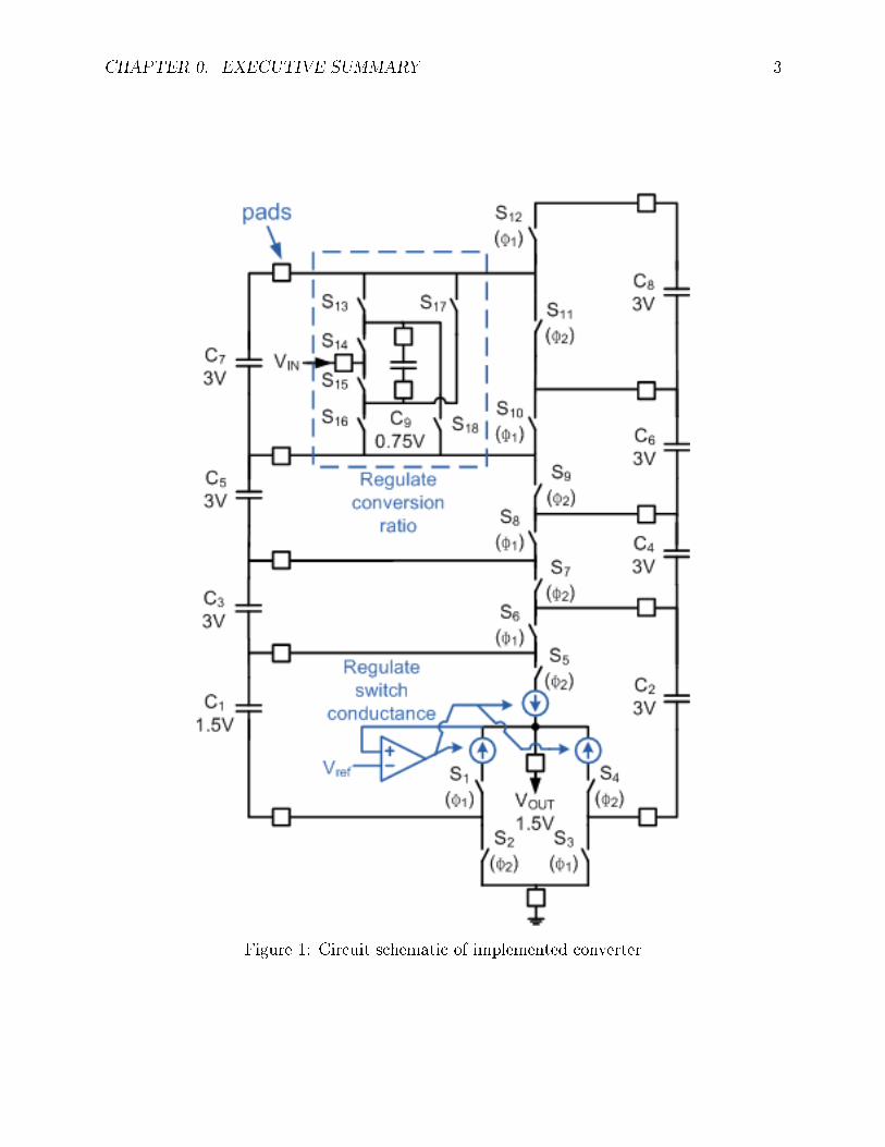
As discussed in references [3, 4] and later in Introduction section 1.2, a number of SCconverter topologies are very eective in their utilization of switches and passive elements,especially in relation to the ever popular buck converter. In terms of switches, the powerswitches in the buck converter each block the full input voltage and support the full outputcurrent. For a large or even moderate conversion ratio, this leads to a high switch total Volt-Ampere product, and causes the buck converter to suer from poor power device utilization.In contrast, the switches in a ladder or Dickson SC converter only block a fraction of theinput voltage, while supporting a fraction of the output current. This not only enablesutilization of native low-voltage CMOS transistors in a modern low-cost CMOS process,but also leads to a low total switch Volt-Ampere product, allowing these SC convertersto sustain high eciency with a high conversion ratio. In terms of passive elements, SCconverters benet from the signicantly higher energy density of capacitors over inductors.As shown in Table 1 [5], surveyed surface mount scale capacitors have a volumetric energydensity that is over 1000 times higher than that of surveyed inductors. This can lead to aconsiderable reduction in Printed Circuit Board (PCB) area and in cost by replacing onebulky inductor with several smaller capacitors. This work builds a moderate conversion ratio
CHAPTER 0. EXECUTIVE SUMMARY 2
Table 1: Energy density of common capacitors and inductors
Type Manufacturer Capacitance Dimensions [mm3] Energy densityCeramic Cap Taiyo-Yuden 22µF@4V 1.6 ∗ 0.8 ∗ 0.8 344µJ/mm3
Ceramic Cap Taiyo-Yuden 1µF@35V 1.6 ∗ 0.8 ∗ 0.8 1196µJ/mm3
Tantalum Cap Vishay 10µF@4V 1.0 ∗ 0.5 ∗ 0.6 533µJ/mm3
Tantalum Cap Vishay 100µ[email protected] 2.4 ∗ 1.45 ∗ 1.1 1037µJ/mm3
Electrolytic Cap Kemet 22µF@16V 7.3 ∗ 4.3 ∗ 1.9 94µJ/mm3
Electrolytic Cap C.D.E 210mF@50V 76φ ∗ 219 172µJ/mm3
Shielded SMT Ind Coilcraft 10µ[email protected] 2.6 ∗ 2.1 ∗ 1.8 0.045µJ/mm3
Shielded SMT Ind Coilcraft 100µ[email protected] 3.4 ∗ 3.0 ∗ 2.0 0.049µJ/mm3
Shielded Inductor Coilcraft 170µ[email protected] 11 ∗ 11 ∗ 9.5 0.148µJ/mm3
Shielded Inductor Murata [email protected] 29.8φ ∗ 21.8 0.189µJ/mm3
(12 V-to-1.5 V) SC converter in a 0.18mm/0.6mm process to realize these advantages of theSC converter.
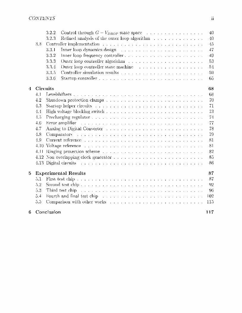
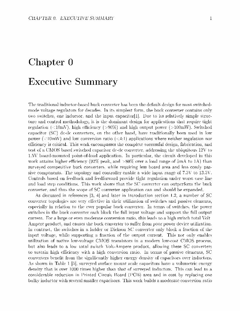
Figure 1 shows the schematic of the Dickson SC converter implemented in this work.The input voltage may range from 7.5V to 13.5V, while the converter outputs a nominalvoltage of 1.5V, dened by an on-chip bandgap reference. Capacitors C1−C9 are the power-train capacitors, and they are implemented with o-chip ceramic capacitors. The Dicksonconverter operates in two phases, and achieves voltage conversion through charge transfersamong capacitors C1 − C9 [6]. Switches S1 − S12 are the power switches, and the phase inwhich they are turned on is indicated by the number in bracket next to the switch labelin the gure; the switch is turned o in the other phase. As further discussed in section2.4, switches S13 − S18 are also power switches, but they may turn on in either clock phasedepending on the conversion ratio of the converter. These switches allow the converter toattain seven dierent conversion ratios, ranging from 5-to-1 to 8-to-1 with half integer steps.As further discussed in section 2.2, the integrated circuit implementation, in a 0.18 microntriple-well CMOS process, is sub-divided into various voltage domains to allow the usage oflow voltage transistors (blocking a maximum of 4V) to accommodate a moderate voltageinput, as high as 13.5V [34]. As further explained in chapter 3, this converter achievesregulation by rst adjusting its nominal conversion ratio, and then by modulating the switchconductance of switches S1,4,5. Switch conductance modulation allows tight regulation forline and load variation whereas changing conversion ratio allows the converter to attain ahigh eciency throughout the operating space. Further, the converter modulates switchingfrequency to attain high eciency at light load conditions. Auxiliary functions such as self-startup, over-current protection and safe shutdown are also implemented. Further details ofthe controller are discussed in chapter 3.
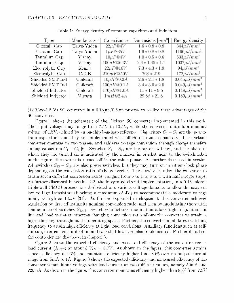
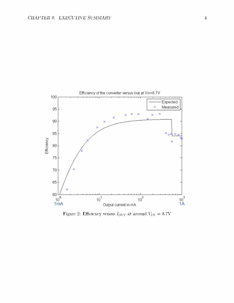
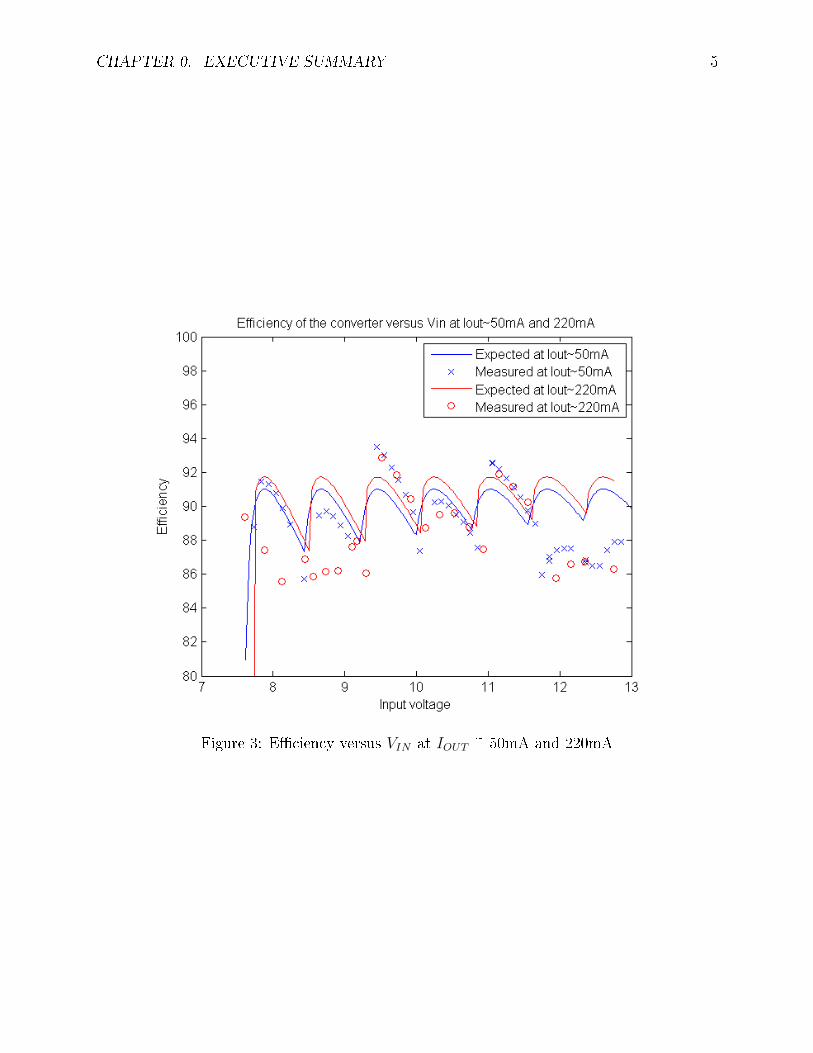
Figure 2 shows the expected eciency and measured eciency of the converter versusload current (IOUT ) at around VIN = 8.7V . As shown in the gure, this converter attainsa peak eciency of 93% and maintains eciency higher than 80% over an output currentrange from 5mA to 1A. Figure 3 shows the expected eciency and measured eciency of theconverter versus input voltage with load current at two dierent values, namely 50mA and220mA. As shown in the gure, this converter maintains eciency higher than 85% from 7.5V
CHAPTER 0. EXECUTIVE SUMMARY 3
Figure 1: Circuit schematic of implemented converter
CHAPTER 0. EXECUTIVE SUMMARY 4
Figure 2: Eciency versus IOUT at around VIN = 8.7V
CHAPTER 0. EXECUTIVE SUMMARY 5
Figure 3: Eciency versus VIN at IOUT ~ 50mA and 220mA
CHAPTER 0. EXECUTIVE SUMMARY 6
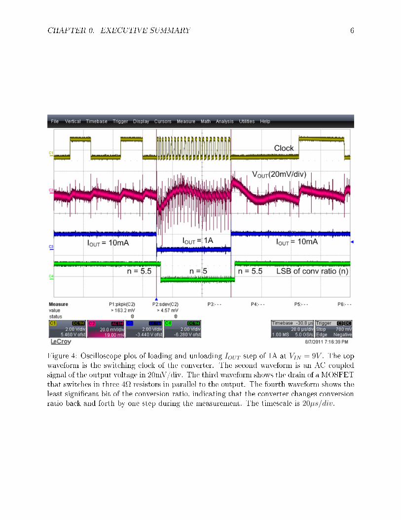
Figure 4: Oscilloscope plot of loading and unloading IOUT step of 1A at VIN = 9V . The topwaveform is the switching clock of the converter. The second waveform is an AC coupledsignal of the output voltage in 20mV/div. The third waveform shows the drain of a MOSFETthat switches in three 4Ω resistors in parallel to the output. The fourth waveform shows theleast signicant bit of the conversion ratio, indicating that the converter changes conversionratio back and forth by one step during the measurement. The timescale is 20µs/div.

CHAPTER 0. EXECUTIVE SUMMARY 7
Figure 5: Comparison of peak eciency between this work and similar works.
to 13V with a nominal output voltage of 1.5V. Figure 4 shows the load transient response ofthe converter during loading and unloading steps of 1A. The output voltage is regulated towithin 30mV during the transient. The behavior of the converter and the controller duringthis transient are discussed in chapter 3 and in chapter 5, section 5.4. Figure 5 shows acomparison of the peak eciency of this converter with that of similarly rated converters.All the surveyed buck and SC converters achieve respectable eciency, but show a generaltrend of reduced eciency as conversion ratio increases. The present work shows a signicantincrease in eciency when compared to similarly rated SC and buck converters. As furtherdiscussed in section 5.5, this work also achieves an overall reduction in PCB area and passivecomponent cost when compared to dc-dc converters with similar ratings. This work showsthat the SC converter, implemented in standard CMOS technology, provides a new directionfor performance and cost advantages with respect to the conventional buck converter. Thiswork shows that the SC converter can outperform the buck converter in areas where thelatter currently dominates, and its scope can be greatly expanded.
CHAPTER 1. INTRODUCTION 8
Chapter 1
Introduction
The traditional inductor-based buck converter has been the default design for most switched-mode voltage regulators for decades. In its simplest form, the buck converter contains onlytwo switches, one inductor, and the input capacitor[1]. Ideally, it can attain any voltage step-down conversion ratio with 100% eciency by varying duty ratio. Due to its relatively simplestructure and control methodology, it is the dominant design for applications that requiretight regulation (<10mV), high eciency (>90%) and high output power (>100mW). TheSwitched Capacitor (SC) dc-dc converter, on the other hand, has its nominal conversion ratiodened by its topology. When an SC converter operates away from its unloaded conversionratio, its eciency suers. Its maximum possible eciency, EffMAX , is given by:
EffMAX =VOUTVIN/n
(1.1)
where VIN is the input voltage, VOUT is the output voltage, and n is the unloaded conversionratio of the converter [3]. In order to attain high eciency across VIN and/or VOUT variations,an SC converter needs to support several conversion ratios, which increases its complexityand the required number of switches and capacitors. Depending on conversion ratio andtopology, an SC converter can have more than a dozen switches and capacitors. Further,as explained in chapter 3, there are numerous ways to control an SC converter. The largenumber of active components (switches) and passive components (capacitors), together withnon-trivial control, has prevented SC converters from becoming the most popular design involtage regulators. Traditionally, SC converters are used in low power (<10mW) applicationswhere regulation and eciency is non-critical. For example, SC converters are used to boostvoltage for the erase function in ash memories. This application uses SC converters becauseerase voltage need not be precise, and low eciency is tolerable since the erase operationis infrequent compared with reading. Applications that require high performance voltageregulators almost all use the buck converter.
However, as explained later in section 1.2, the SC converter can be superior to the buckconverter in terms of both cost and eciency. This allows the SC converter to be verycompetitive in dc-dc converter markets, where the buck converter currently dominates. Thiswork aims to address the challenges in designing and controlling the SC converter, and tounleash the full potential of the Switched Capacitor dc-dc converter.
CHAPTER 1. INTRODUCTION 9
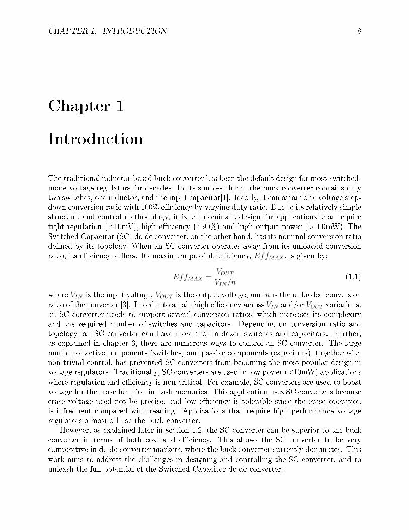
Figure 1.1: Basic model for an SC converter
1.1 The model used for SC converter
Before a discussion of the benets of using an SC converter, a review of the SC convertermodel and operation is provided in this section. This model has been discussed in references[2, 3, 5, 4], so only a brief summary will be included here. Figure 1.2(a) shows a simple 3:1SC converter using the Dickson topology[6]. This SC converter is a two phase circuit withnominally 50% duty cycle. By connecting the power-train capacitors dierently in the twoclock phases, the SC converter attains the nominally 3:1 voltage conversion ratio by chargesharing among the capacitors. As a beginning step [3], an SC converter can be modeled asan ideal transformer in series with an output referred resistance, ROUT , as shown in gure1.1. The turns ratio in the ideal transformer represents the unloaded conversion ratio of theconverter. When the converter is loaded, this necessitates a voltage drop across the converterdue to charge transfer and conduction loss, and this is represented by a voltage drop acrossROUT . There are two asymptotic limits to ROUT , the slow switching limit (SSL), and thefast switching limit (FSL). In the SSL, capacitors are allowed to fully equilibriate withineach clock phase, and charge transfer can be modeled as impulsive. In this limit, ROUT isdetermined only by the switching frequency of the converter and the capacitors in the circuit,as explained in subsection 1.1.1. In the FSL, capacitor voltages remain constant, and currentow is modeled as being constant within each clock phase. In this limit, ROUT is determinedonly by switches and other resistances in the converter, as explained in subsection 1.1.2. Acombined result will be discussed in subsection 1.1.3.
This simplied model captures the series conduction loss of an SC converter. Other majorlosses, namely switching loss due to gate switching, can be modeled as parallel losses. Thiscan be modeled as a resistor in parallel with the output terminal in gure 1.1. For simplicitythis resistor is not included in the model but switching loss will be discussed separately insubsection 1.2.3.
1.1.1 SSL model of SC Converter
In the asymptotic slow switching limit (SSL), the output referred resistance ROUT , denotedas RSSL, is given by:
RSSL =∑iεcaps
(ac,i)2
fSWCi(1.2)
CHAPTER 1. INTRODUCTION 10
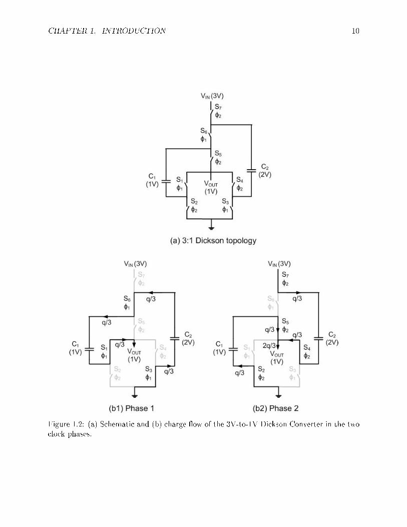
Figure 1.2: (a) Schematic and (b) charge ow of the 3V-to-1V Dickson Converter in the twoclock phases.
CHAPTER 1. INTRODUCTION 11
where fSW is the switching frequency of the converter, and Ci stands for the capacitance ofcapacitor Ci. Coecient ac,i is called the charge multiplier coecient; it is the ratio betweenthe charge ow per period in Ci and the total output charge ow per period in steady state.Using the charge ow diagram of a 3:1 Dickson Converter [6] in gure 1.2 as an example, onecan see that the total charge ow to the output is q, and the charge ow in both capacitorsC1 and C2 are q/3. Thus ac,1 = ac,2 = 1/3. If C1 = C2 = 1µF and fSW = 1MHz, RSSL iscalculated to be 2/9Ω.
For a given RSSL and frequency, one can optimally size Ci to give the lowest total capac-itor energy storage requirement. This energy, denoted as ETOT , is given by:
ETOT =∑iεcaps
1
2Ci(vc,i(rated)
)2(1.3)
where vc,i(rated) is the rated voltage of the capacitor. The rated voltage of the capacitor needsto be at least its blocking voltage, and is subjected to the constraint of available technology.In gure 1.2, the blocking voltage of capacitor C2 is 2V , and thus vc,2(rated) > 2V . Theoptimally sized Ci is given by:
Ci =
∣∣∣∣ ac,ivc,i(rated)
∣∣∣∣ 2ETOT∑kεcaps
∣∣ac,kvc,k(rated)∣∣ (1.4)
and the resulting RSSL is given by:
RSSL =1
2ETOTfSW
(∑iεcaps
∣∣ac,ivc,i(rated)∣∣)2
(1.5)
For the circuit in gure 1.2, using a target RSSLof 2/9Ω, fSW = 1MHz and vc,i(rated)equals to the respective blocking voltage, equation 1.5 shows that ETOT = (9/4)µJ . Usingequation 1.4, one can show that the optimal sizing is C1 = 1.5µF and C2 = 0.75µF . SinceETOT is roughly proportional to the printed circuit board (PCB) area of discrete capacitorsor silicon area of integrated capacitors, this optimization methodology can help to attain thesmallest PCB footprint or silicon area of an SC converter for a given RSSL.
1.1.2 FSL model of SC Converter
In the asymptotic fast switching limit (FSL), the output referred resistance ROUT , denotedas RFSL, is given by:
RFSL =∑
iεswitches
∑jεphases
Ri
Dj
(ajr,i)2
(1.6)
where Ri is the resistance of switch Si or other parasitic resistances, and Dj is the duty ratioof the jth phase. Coecient ajr,i is the charge multiplier coecient, dened similarly to ac,iin SSL. It is the ratio between the charge ow per period in Si in phase j and the totaloutput charge ow per period in steady state. In gure 1.2, switch S1 conducts charge q/3in phase 1, but is o in phase 2. Thus a1r,1 = 1/3 and a2r,1 = 0. For the circuit in gure 1.2,
CHAPTER 1. INTRODUCTION 12
if each of the switches has a resistance of 1Ω and both clock phases have 50% duty ratio(Dj = 0.5), one can show that RFSL = 14/9Ω.
Similar to capacitors in SSL, there exists an optimal set of switch sizes that will give arequired RFSL while minimizing the total switch size, referred to as ATOT . In an integratedcircuit, this quantity is roughly proportional to area. This cost function, ATOT , is given by:
ATOT =∑
iεswitches
Gi
(vr,i(rated)
)2(1.7)
where Gi = 1/Ri is the conductance of switch Si, and vr,i(rated) is its rated voltage. Analo-gously to capacitors, the rated voltage of the switch needs to be at least its blocking voltage,and is subjected to the constraint of available technologies. For the circuit in gure 1.2,switch S6 blocks 2V , whereas all other switches block 1V . The cost function, represented byequation 1.7, reects typical technology behavior in both CMOS (complimentary metal oxidesemiconductor) and LDMOS (laterally diused metal oxide semiconductor) switches. Whenpractical devices deviate from this assumption, one can account for this by using a methodsimilar to the one outlined in section 2.3. If only switch resistances are being considered andduty ratio D1 = D2 = D, the optimal switch conductance Gi is given by:
Gi =
∣∣∣∣ ar,ivr,i(rated)
∣∣∣∣ ATOT∑kεswitched
∣∣ar,kvr,k(rated)∣∣ (1.8)
and the resulting RFSL is given by:
RFSL =1
D ∗ ATOT
( ∑iεswitches
∣∣ar,ivr,i(rated)∣∣)2
(1.9)
For the circuit in gure 1.2, using a target RFSL of 14/9Ω, D1 = D2 = 0.5 and vr,i(rated)equal to the respective switch blocking voltage, equation 1.9 shows that ATOT = 64/7.Using equation 1.8, one can show that the optimal sizing is G6 = 4/7, and Gi = 8/7 for allother switches. Since ATOT roughly corresponds to the die area of integrated switches, thisoptimization methodology can help to attain the smallest die area of an SC converter for agiven RFSL.
1.1.3 Combined model of SC Converter
While subsections 1.1.1 and 1.1.2 discuss output referred resistances (ROUT ) in the SSLand the FSL, a real design usually lies somewhere between these two asymptotic limits. Inthe intermediate region, charge ow between capacitors in each clock phase will be neitherimpulsive nor constant, but will decay with a settling time constant. Deriving an alge-braic expression for ROUT in this region is inconvenient [5], but it can be approximated bycombining RSSL and RFSL as follows:
ROUT ≈√R2SSL +R2
FSL (1.10)
When the cost of both capacitors and switches are important, the optimal design strategywill be to set RSSL ≈ RFSL, and then to independently optimize capacitors and switches
CHAPTER 1. INTRODUCTION 13
using the methodology outlined in subsections 1.1.1 and 1.1.2, respectively. If the designis capacitor constrained, one may want to pick RSSL > RFSL and vice versa if the designis switch constrained. The analysis and optimization methodology outlined in this sectionare very useful in evaluating and designing an SC converter, and they will be the basis fordiscussions in the following sections and chapters. Further background information can befound in reference [5] for the interested reader.
1.2 Advantages of SC converters
The main criteria for evaluating voltage regulators are: component costs, power eciency,and regulation performance. This section will show that the SC converter is advantageous inboth costs and eciency when compared to the inductor-based buck converter - the dominantarchitecture for dc-dc converters. Regulation, however, can be a concern, and it will bediscussed in detail in chapter 3. The component costs of a dc-dc converter can be divided intotwo main categories, active elements (switches) or passive elements (capacitors or inductors),and can be measured in terms of manufacturing cost, PCB area, and die area. Subsections1.2.1 and 1.2.2 will use these metrics to discuss active and passive elements respectively. Thepower loss of a dc-dc converter can also be divided into two main categories, conduction lossand switching loss. Conduction loss of a dc-dc converter is a series loss component and isdominated by its active elements and passive elements. Switching loss, on the other hand,is a parallel loss and will be discussed separately in subsection 1.2.3. While there are manydierent SC converter topologies, this section will focus on the Dickson topology [6] since itis the topology chosen in this work. The reason for choosing the Dickson topology will bediscussed in section 2.1.
1.2.1 Active element analysis
To compare active element (switches) utilization among power converters, one can use theswitch stress parameter G−V 2 product [31]. A higher G−V 2 product means higher switchstress, and it usually entails more costly or larger PCB area for discrete switches or a largerdie area for integrated switches with a target power loss. The G−V 2 switch stress of an SCconverter is compared to the buck converter using an example given in gure 1.3. Figure1.3a shows an SC converter using the Dickson topology, whereas gure 1.3b shows a buckconverter. Both converters are stepping down from 10V to 1V and with an output currentof 1A. A comparison between these two converters is done by comparing the eective outputresistance, ROUT , of both converters for a given cost function, ATOT , as shown in equation1.7. For simplicity, ATOT is set to be 1 in the comparison.
In terms of the SC converter, as discussed in section 1.1, switches only matter in the FSLcalculations but not in the SSL calculations, and thus this subsection will focus on an SCconverter operating in the FSL. Although peak current through a switch is innite in SSL,the switches can be reduced in size to lower this peak current without deteriorating ROUT .Thus the real switch stress of an SC converter can be evaluated when it is operating in theFSL, and can no longer reduce peak current without aecting ROUT . For the example ingure 1.3a, the charge multiplier coecients, ar,5−14, = 1/10 for switches S5 − S14, whereas
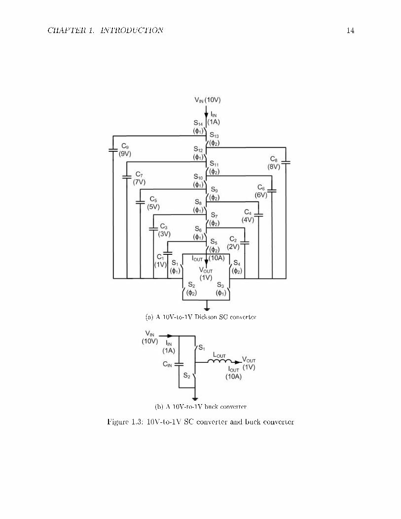
CHAPTER 1. INTRODUCTION 14
(a) A 10V-to-1V Dickson SC converter
(b) A 10V-to-1V buck converter
Figure 1.3: 10V-to-1V SC converter and buck converter
CHAPTER 1. INTRODUCTION 15
ar,1,2 = 5/10 and ar,3,4 = 4/10 for switches 1,2 and 3,4 respectively. In terms of blockingvoltage, switches S1−S5 block 1V whereas switches S6−S13 block 2V . Thus using equation1.9, the output impedance ROUT (∼ RFSL) of the SC converter equals is 26Ω for D =0.5 and when ATOT = 1. In terms of the buck converter, since the duty factor is 0.1,ROUT = 0.1/G1 + 0.9/G2, where G1 and G2 are the switch conductance of switches S1 andS2 respectively. The optimal sizing of switches S1 and S2 is such that G2 = 3G1. Sinceboth switches block 10V, ATOT =
∑GV 2 = 400G1. Setting ATOT = 1, G1 = 1/400. Thus
ROUT = 0.1/G1 + 0.9/G2 = 160 for the buck converter.In this simple example, the buck converter has an output impedance, ROUT , that is more
than seven times as high as that of the SC converter, and thus the SC converter is muchsuperior in terms of switch utilization. As shown in references [3, 5], this advantage increasesfurther as conversion ratio increases, and this makes the SC converter even more favorable.References [5, 4] further show that the Dickson SC converter is at the switch utilizationfundamental limit of dc-dc converters derived in [7], meaning that no other dc-dc converter,whether inductor-based or capacitor-based, can have a better switch utilization than theDickson SC converter.
Further, the Dickson SC converter only requires low voltage transistors, making it possibleto only use native transistors in a CMOS process. The buck converter, on the other hand,requires high voltage transistors, and thus may require LDMOS transistors when switchesare integrated. This can increase the complexity of the process and increase manufacturingcost. However, if discrete transistors are used, it may be possible to manufacture the highvoltage transistors with a low cost legacy technology. As a conclusion for switches, due toits low G−V 2 product and low switch blocking voltage, the Dickson SC converter will likelyhave lower manufacturing cost, smaller die area, and thus lower overall cost for switches.
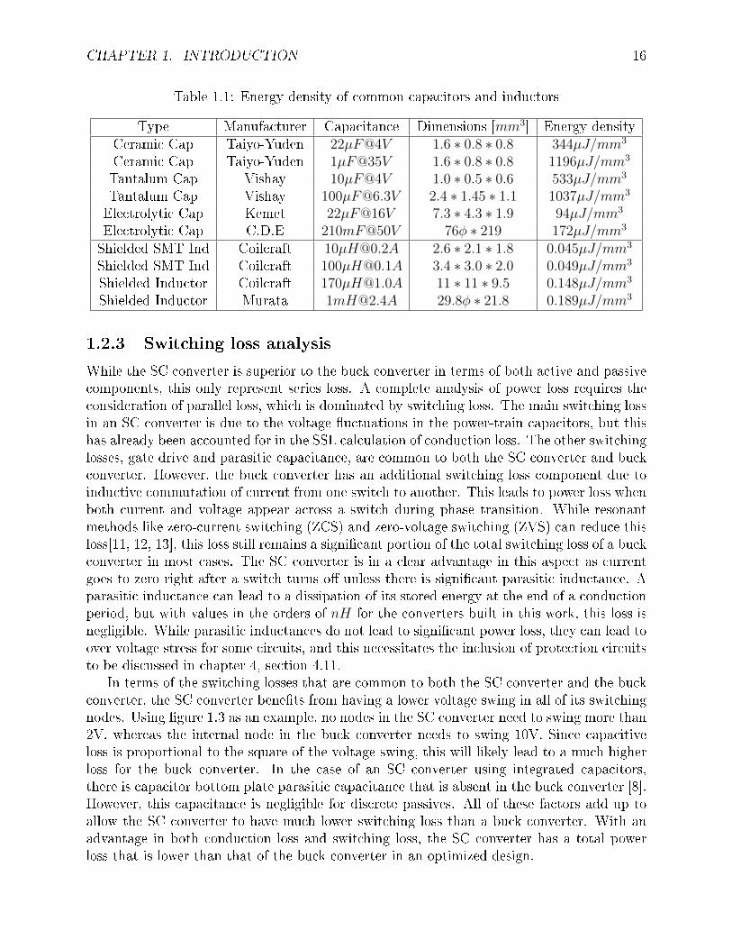
1.2.2 Passive element analysis
The Dickson topology chosen in this work is superior in switch utilization, but not in capac-itors when compared to other SC topologies [3]. However, its passive component utilizationand that of other SC topologies are still superior to the buck converter when one takes intoaccount the comparative energy density of capacitors and inductors. Table 1.1 shows thedimension and energy density of representative discrete capacitors and inductors [5]. Byinspection, surveyed capacitors have a volumetric energy density that is over 1000 timeshigher than that of surveyed inductors. This more than compensates for the weaker reactiveelement utilization of the Dickson topology when compared with the buck converter andother SC topologies [4]. Moreover, as will be shown in section 5.5, discrete capacitors usedin SC converters are usually an order of magnitude cheaper than the discrete inductors usedin buck converters. When integrated passives are used, references [8, 4] further shows thatan SC converter can achieve a power density that is orders of magnitude higher than thatof the buck converter [9, 10]. With a superior passive component utilization, SC converterscan potentially have lower passive component cost and PCB/die area for a given amountof power loss, or equivalently attain a higher eciency with the same amount of resources,when compared to the buck converter.
CHAPTER 1. INTRODUCTION 16
Table 1.1: Energy density of common capacitors and inductors
Type Manufacturer Capacitance Dimensions [mm3] Energy densityCeramic Cap Taiyo-Yuden 22µF@4V 1.6 ∗ 0.8 ∗ 0.8 344µJ/mm3
Ceramic Cap Taiyo-Yuden 1µF@35V 1.6 ∗ 0.8 ∗ 0.8 1196µJ/mm3
Tantalum Cap Vishay 10µF@4V 1.0 ∗ 0.5 ∗ 0.6 533µJ/mm3
Tantalum Cap Vishay 100µ[email protected] 2.4 ∗ 1.45 ∗ 1.1 1037µJ/mm3
Electrolytic Cap Kemet 22µF@16V 7.3 ∗ 4.3 ∗ 1.9 94µJ/mm3
Electrolytic Cap C.D.E 210mF@50V 76φ ∗ 219 172µJ/mm3
Shielded SMT Ind Coilcraft 10µ[email protected] 2.6 ∗ 2.1 ∗ 1.8 0.045µJ/mm3
Shielded SMT Ind Coilcraft 100µ[email protected] 3.4 ∗ 3.0 ∗ 2.0 0.049µJ/mm3
Shielded Inductor Coilcraft 170µ[email protected] 11 ∗ 11 ∗ 9.5 0.148µJ/mm3
Shielded Inductor Murata [email protected] 29.8φ ∗ 21.8 0.189µJ/mm3
1.2.3 Switching loss analysis
While the SC converter is superior to the buck converter in terms of both active and passivecomponents, this only represent series loss. A complete analysis of power loss requires theconsideration of parallel loss, which is dominated by switching loss. The main switching lossin an SC converter is due to the voltage uctuations in the power-train capacitors, but thishas already been accounted for in the SSL calculation of conduction loss. The other switchinglosses, gate drive and parasitic capacitance, are common to both the SC converter and buckconverter. However, the buck converter has an additional switching loss component due toinductive commutation of current from one switch to another. This leads to power loss whenboth current and voltage appear across a switch during phase transition. While resonantmethods like zero-current switching (ZCS) and zero-voltage switching (ZVS) can reduce thisloss[11, 12, 13], this loss still remains a signicant portion of the total switching loss of a buckconverter in most cases. The SC converter is in a clear advantage in this aspect as currentgoes to zero right after a switch turns o unless there is signicant parasitic inductance. Aparasitic inductance can lead to a dissipation of its stored energy at the end of a conductionperiod, but with values in the orders of nH for the converters built in this work, this loss isnegligible. While parasitic inductances do not lead to signicant power loss, they can lead toover voltage stress for some circuits, and this necessitates the inclusion of protection circuitsto be discussed in chapter 4, section 4.11.
In terms of the switching losses that are common to both the SC converter and the buckconverter, the SC converter benets from having a lower voltage swing in all of its switchingnodes. Using gure 1.3 as an example, no nodes in the SC converter need to swing more than2V, whereas the internal node in the buck converter needs to swing 10V. Since capacitiveloss is proportional to the square of the voltage swing, this will likely lead to a much higherloss for the buck converter. In the case of an SC converter using integrated capacitors,there is capacitor bottom plate parasitic capacitance that is absent in the buck converter [8].However, this capacitance is negligible for discrete passives. All of these factors add up toallow the SC converter to have much lower switching loss than a buck converter. With anadvantage in both conduction loss and switching loss, the SC converter has a total powerloss that is lower than that of the buck converter in an optimized design.
CHAPTER 1. INTRODUCTION 17
1.3 Target applications of this work
After discussing the advantages of the SC converter in section 1.2, the following chapters willdiscuss the methods to realize them in a real design. The point-of-load application is chosenas the target application because it is an important one dominated by the buck converter.By showing the superiority of the SC converter in this area, this work will show that theapplications for SC converters can be greatly expanded. The specication of this work is adc-dc converter stepping down to 1.5V with an input voltage range of 7.5V-13V, and withan output current of 1A.
This moderate conversion ratio is chosen because it is common for many applications.For example, the laptop computer power converter may need to step down from 10-16V downto 1-2V. Further, most telecommunication and network switching systems include on-boardpower supplies that step down from 12V to 1-2V. This market is currently dominated bythe buck converter and constitutes a signicant proportion of the overall dc-dc convertermarket. This market section requires a conversion ratio that has not been attempted byany SC converters to the best of the author's knowledge. Most SC converters operate witha conversion ratio of less than 4-to-1, and thus a successful 8-to-1 SC converter expandsthe scope of SC converters into this vast market. Coincidentally, the benets of using anSC converter increase with higher conversion ratio, and thus this choice of conversion ratiois also a strategic opportunity to showcase the superiority of the SC converter. A higherconversion ratio is not chosen because the number of components and complexity of theconverter increases with conversion ratio. A moderate conversion ratio represents a trade-obetween the potential relative benet and the complexity of the circuit.
The moderate output current of 1A is chosen because this current level is signicantlyhigher than the typical values for SC converters in the market. Most SC converters notonly have a low conversion ratio, but also have current levels below 100mA. However, manyapplications dictate load current well above 1A, for example a microprocessor can draw upto 100A of current. Being able to supply high current is an important market segment aselectronics become more power hungry. These applications are exclusively dominated bythe buck converter, and thus it will be groundbreaking to show that the SC converter notonly can achieve similar results but can do even better. A load current level exceeding 1Ais not chosen because those converters are usually multi-phase and built with many smallerconverters bundled together. Although one can apply multi-phase technique to SC convertersas well, this nonetheless adds another layer of complexity to the design. Since the purpose ofthis work is path-nding, it is strategic to limit the complexity and not try to reach the endgoal in one step. An output current level of 1A is a typical current level for a single phasebuck converter in the market, and thus using a single phase SC converter for this work willbe a fair comparison.
In terms of integration, most buck converters with similar conversion ratio and outputcurrent use integrated switches and o-chip inductors. Thus this work utilizes integratedswitches and o-chip passives, namely capacitors, as well. The chips fabricated in this workutilize the 0.18µm/0.6µm (CMOS + LDMOS) process from National Semiconductor. Thistechnology node is popular among power converters for this application. Chapters 2 and3 discuss the architecture and control algorithm of this work, and chapter 4 discusses thecircuit designs. Chapter 5 discusses the test results of the test chips, and compares them
CHAPTER 1. INTRODUCTION 18
with other works from industry and literature. The culminating test chip obtains a peakeciency of 92%, and maintains an eciency higher than 80% from 5mA to 1A of outputcurrent. This performance not only far exceeds that of the surveyed SC converters, but alsoexceeds that of surveyed buck converters. Further, the PCB footprint of the capacitors inthis work is only a fraction of the PCB footprint area of the inductors in the surveyed buckconverters. These results show that the SC converter can be more than competitive in anarea where the buck converter has dominated for decades. Chapter 6 concludes this workand discusses future opportunities to further expand the potential of the SC converter.
CHAPTER 2. ARCHITECTURE 19
Chapter 2
Architecture
After discussing the motivation and specication of this work in Chapter 1, this chapterdiscusses the architecture of the converter. A 12V-to-1.5V dc-dc converter is implementedusing o-chip ceramic capacitors and integrated switches in a 0.18µm/0.6µm process. Ce-ramic capacitors are chosen due to their high energy density and low RESR(equivalent seriesresistance). These attributes allow a low ROUT while having a small PCB footprint. Theswitching frequency of the converter can be varied, and is designed to go up to 5MHz. Vary-ing switching frequency can be used to optimize power loss [19] as explained in subsection2.3.3, or to achieve regulation [21] as explained in section 3.1. The frequency is limited at5MHz because the ESR corner frequency of the ceramic capacitors is around this frequencyand going beyond this point has little benet in either eciency or regulation. The followingsections will discuss in detail the architecture of the converter, and the ways to achieve thebest performance.
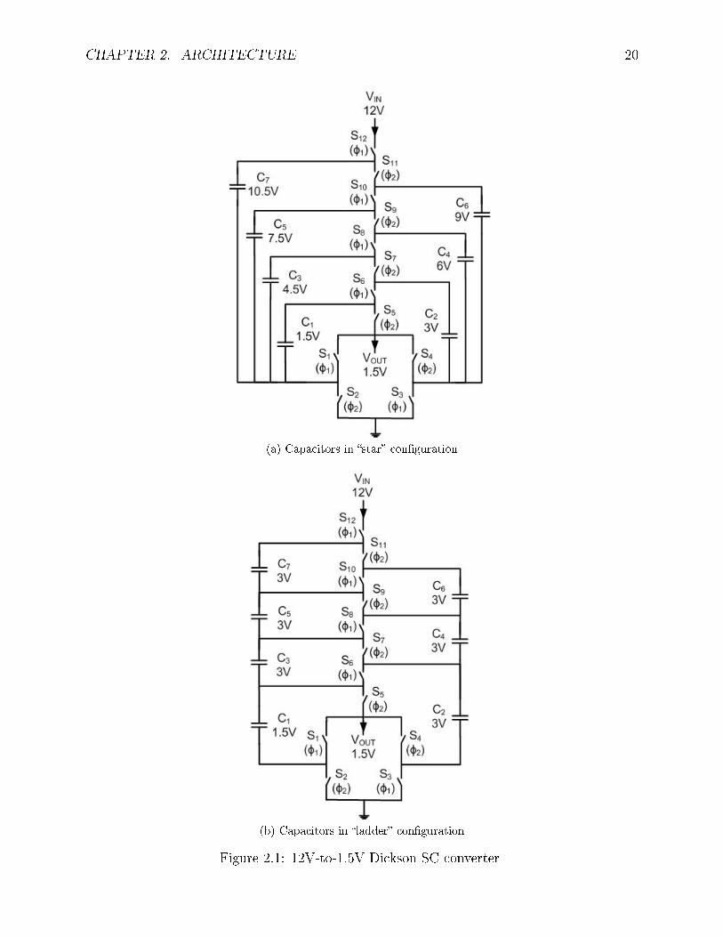
2.1 Topology choice
The topology chosen is the 12V-to-1.5V (8:1) Dickson converter. It is shown in gure 2.1with two dierent capacitor congurations: (a) star and (b) ladder. In terms of switches,these two congurations are identical, with the same blocking voltage and current ow foreach switch. In terms of capacitors, by using equation 1.5, one can show that they bothrequire the same total capacitor energy storage capacity (ETOT , eq. 1.3) to achieve a givenoutput referred resistance in the slow switching limit (RSSL). These two congurations arebasically equivalent but have subtle dierences in practice. Although both congurationsgive the same ETOT requirement, ceramic capacitors have a higher energy density per volumefor a part with a higher rated voltage. Since the star conguration uses higher voltagecapacitors, it will benet from a higher ETOT and thus have a lower RSSL for a given volumeof ceramic capacitors. However, the ladder conguration has a more favorable transientresponse than the star conguration. For example, when the input voltage increases, all thecapacitor voltages will have to increase since the conversion ratio is xed at 8-to-1. The ladderconguration will allow this to occur more uniformly since the capacitors are connected inseries. On the other hand, the star conguration would require several switching periodsbefore the equilibrium voltage levels are reached. Thus the ladder conguration should be
CHAPTER 2. ARCHITECTURE 20
(a) Capacitors in star conguration
(b) Capacitors in ladder conguration
Figure 2.1: 12V-to-1.5V Dickson SC converter
CHAPTER 2. ARCHITECTURE 21
used when line regulation is taken into account.There are many SC converter topologies, and for those compared and contrasted in [3],
some are better in terms of switch utilization while others are better in terms of capacitorutilization. The Dickson topology chosen in this work has good switch utilization but is notas good in terms of capacitor utilization. This work made this choice because capacitance isin abundance due to the usage of o-chip capacitors but switches are integrated and a largerdie area leads to a higher cost. When compared to the other topologies that have similarswitch utilization, for example the ladder topology, the Dickson converter is chosen becauseit has fewer capacitors. This gives a minimum number of I/O pins and o-chip components.These translate to a lower pad overhead on the die, and a smaller PCB footprint and thusa lower cost for the converter.
Considering the implementation of the switches, the process used in this work has twochoices of CMOS transistors: the 0.18µm transistor with a rated voltage of 1.8V and the0.6µm transistor with a rated voltage of 5V. Switches S1−S5 block 1.5V and are implementedwith 1.8V transistors; whereas switches S6−S11 need to block 3V and are implemented with5V transistors. Switch S12 only needs to block 1.5V, but due to the way in which switchesare driven, as explained in section 2.2, it is also implemented with a 5V transistor. Sincethese voltage blocking levels match well with these devices, this process is a very appropriatechoice. All of these switches are driven in a two phase manner as indicated in gure 2.1.The conguration in each phase can be obtained by using a diagram similar to gure 1.2.The two phase clocks are non-overlapping to prevent direct current ow that can short outa power-train capacitor and cause signicant power loss.
2.2 Multiple voltage domains
The converter is subjected to an input voltage of 12V, and yet it is made up of transistorswith a rated voltage of 5V or less. In order to prevent over-voltage stress of any of thesedevices, the silicon chip is divided into numerous voltage domains isolated from the substrateby deep n-well structures. Communication across voltage domains is achieved by using thelevelshifter circuit discussed in section 4.1. Figure 2.2 shows the 9 dierent voltage domains inthe converter, and the arrows next to the switches indicate which voltage domain the switchresides in. This gure uses the ladder-type capacitor conguration, but a similar design canalso be obtained by using the star-type capacitor conguration. When compared with gure2.1b, gure 2.2 has 1 more capacitor, C8, and 1 more switch, S13. These two componentsare added to create voltage domain 9 that drives switches S11 and S12. This is a 3V voltagedomain, and thus switch S12 is implemented with 5V transistor even though it only needsto block 1.5V. When compared to gure 2.1b, switch S12 is connected to the top plate of C8
instead of C7. These two implementations of S12 are equivalent since when S12 turns on inclock phase 1, the top plate of C7 and C8 are connected. Switch S12 is implemented this wayso that it can be a PMOS transistor driven easily by voltage domain 9. Although capacitorC8 can be implemented with much reduced capacitance, it is nonetheless implemented witho-chip ceramic capacitors for the sake of uniformity. There may be benets in moving iton-chip and reducing the required PCB area.
By separating the die into dierent voltage domains, no switch sees a voltage stress higher
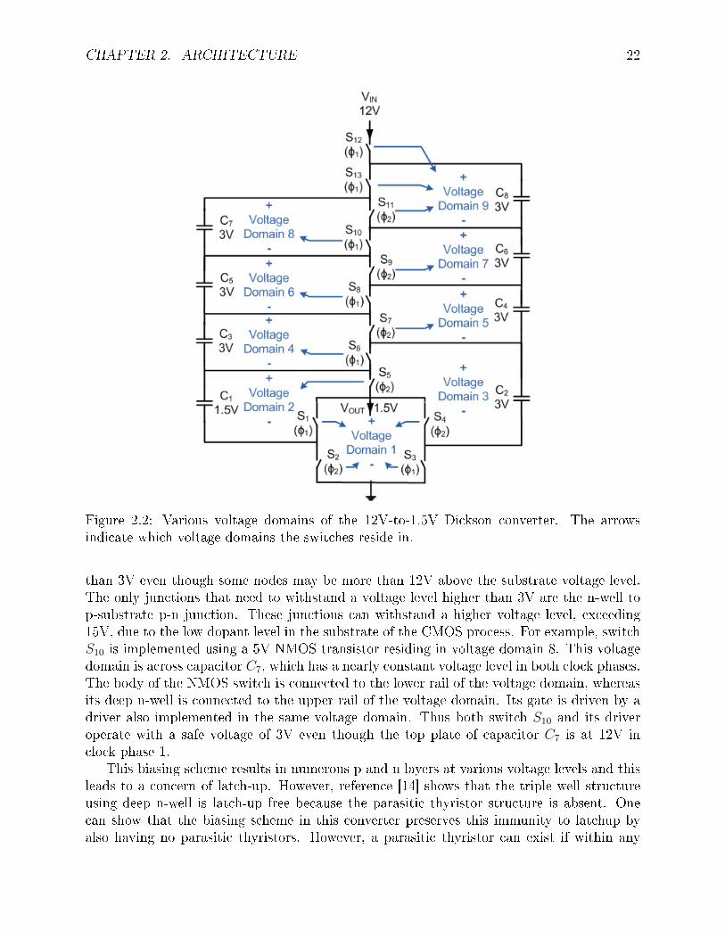
CHAPTER 2. ARCHITECTURE 22
Figure 2.2: Various voltage domains of the 12V-to-1.5V Dickson converter. The arrowsindicate which voltage domains the switches reside in.
than 3V even though some nodes may be more than 12V above the substrate voltage level.The only junctions that need to withstand a voltage level higher than 3V are the n-well top-substrate p-n junction. These junctions can withstand a higher voltage level, exceeding15V, due to the low dopant level in the substrate of the CMOS process. For example, switchS10 is implemented using a 5V NMOS transistor residing in voltage domain 8. This voltagedomain is across capacitor C7, which has a nearly constant voltage level in both clock phases.The body of the NMOS switch is connected to the lower rail of the voltage domain, whereasits deep n-well is connected to the upper rail of the voltage domain. Its gate is driven by adriver also implemented in the same voltage domain. Thus both switch S10 and its driveroperate with a safe voltage of 3V even though the top plate of capacitor C7 is at 12V inclock phase 1.
This biasing scheme results in numerous p and n layers at various voltage levels and thisleads to a concern of latch-up. However, reference [14] shows that the triple well structureusing deep n-well is latch-up free because the parasitic thyristor structure is absent. Onecan show that the biasing scheme in this converter preserves this immunity to latchup byalso having no parasitic thyristors. However, a parasitic thyristor can exist if within any
CHAPTER 2. ARCHITECTURE 23
voltage domain, the n-well of a PMOS device is merged with the deep n-well of an NMOSdevice [15]. This creates a parasitic thyristor similar to the familiar case in a non-triple-wellCMOS process [16]. However, this threat of latch-up is no greater than that in the familiarCMOS case, and should already have been considered when the design rules were written.Nonetheless, by the virtue of conservative layout, this layout merger is avoided in this work,and the two types of transistors are always placed in separate wells. Latch-up has not beenobserved during testing of any version of the fabricated devices.
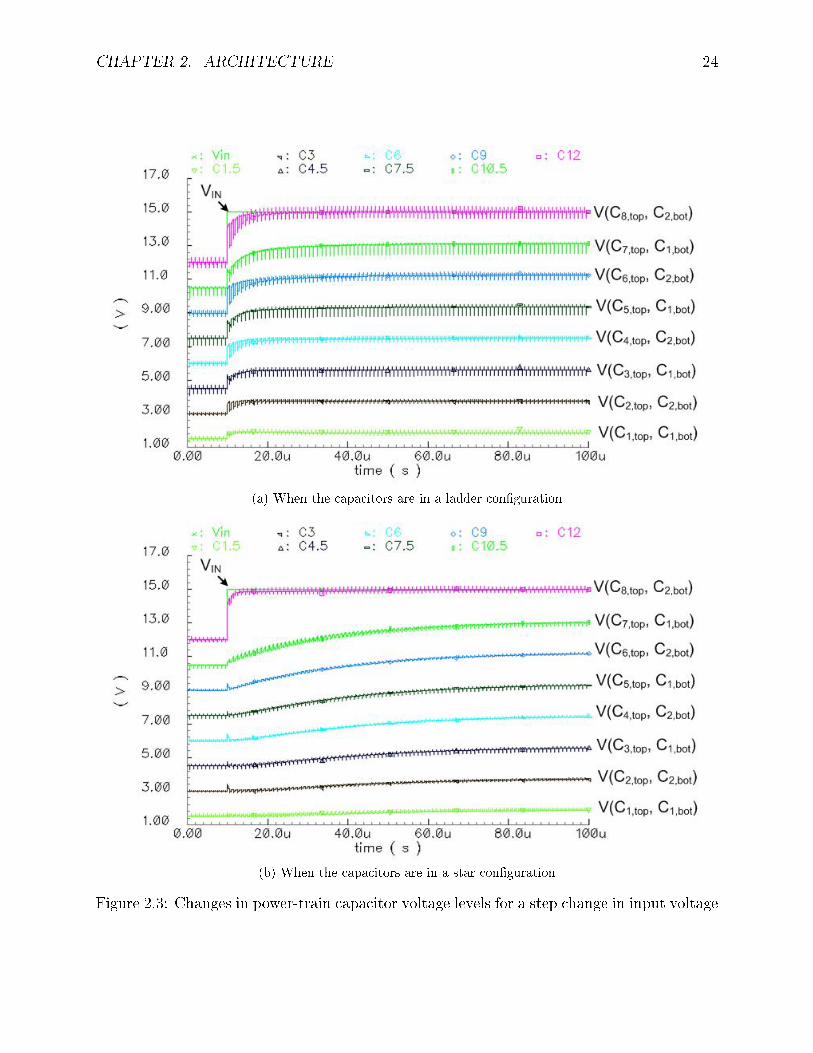
One consideration of using voltage domains dened by power train capacitors is that italso favors the usage of the ladder type capacitor conguration over the star type capacitorconguration. When there is a rapid change in the input voltage, all power-train capacitorvoltages will change in the same direction if the capacitor conguration is ladder-type. Thisspreads out the change in input voltage by capacitive division. On the other hand, if a starconguration is being used, only the voltage of capacitor C7 in gure 2.1a will change initially,and it will take many clock cycles before the other capacitors reach the new equilibriumvoltage levels. This is illustrated by simulation results shown in gure 2.3. The simulationsshow how the power-train capacitor voltage levels change when the input voltage steps from12V to 15V. Figure 2.3a shows the case when a ladder conguration is used, whereas gure2.3b shows the case when a star conguration is used. The converter is switching at a constantfrequency of 1MHz in both cases. In both cases, the top plate of C8 is pulled up immediatelysince the body diode of PMOS transistor S12 is turned on. As shown in the simulations,the star conguration takes signicantly longer time to attain symmetric division among thevoltage levels. More signicantly, in the simulation of the star conguration in gure 2.3b,the voltage level of voltage domain 9 is increased substantially with respect to the othervoltage domains in the beginning of the transient. This can cause the levelshifter circuitdiscussed in section 4.1 to fail. This is a major consideration that motivates the use of theladder conguration. It can be shown that a similar eect occurs when the conversion ratioof the converter changes. Design for multiple conversion ratios is discussed in section 2.4.
2.3 Device sizing and optimization
2.3.1 Capacitor Sizing
After determining the topology of the converter, one needs to choose the individual sizes ofeach capacitor and switch to minimize PCB area and die area. For all the o-chip capacitors,the high value multilayer ceramic capacitors with size 0603 (16mm*8mm) from Taiyo-Yudenwith code X5R are chosen. Size 0603 capacitors are chosen for their high capacitance, whichreduces RSSL to a fraction of RFSL at a switching frequency of 1MHz, as discussed in chapter5. There may be a strategic choice in using smaller size capacitors to reduce PCB area, butthis route is not taken because 0402 capacitors have signicantly reduced energy density.The capacitance of each capacitor is then picked by choosing the part with the maximumcapacitance that has an ESR corner frequency exceeding 5MHz and with a rated voltageexceeding the blocking voltage requirement. The optimization scheme outlined in subsection1.1.1 is not used because the major cost, PCB area, is xed and does not scale with ETOT asdened by equation 1.3. However, the optimization scheme can be useful if capacitor sizes
CHAPTER 2. ARCHITECTURE 24
(a) When the capacitors are in a ladder conguration
(b) When the capacitors are in a star conguration
Figure 2.3: Changes in power-train capacitor voltage levels for a step change in input voltage
CHAPTER 2. ARCHITECTURE 25
are more granular in a dierent design setting.
2.3.2 Switch sizing
The switches in this design are integrated and their sizes can vary smoothly. Thus, unlikethe capacitors, the optimization scheme outlined in subsection 1.1.2 becomes useful. Insteadof using the scheme directly, this work modies it slightly to reect the actual data fromthe process. The cost function being optimized, as dened in equation 1.7, assumes thatswitch area is proportional to GV 2
rated, where G is the conductance of the switch and Vratedis its rated voltage. While this assumption is roughly true for the active area of a CMOStransistor, a real transistor layout deviates from this due to many factors, including carriermobility, gate drive, contact layout overhead etc. However, one can capture most of thesefactors by assigning a number to V 2
rated that need not be the rated voltage of the switch.Parameter V 2
rated is a weight in the optimization to capture the relative cost of the dierenttypes of switches, and it can be used to capture any factor that the designer considers. Inthis work, it is used to capture the real layout area of switches. First, V 2
rated is set to 1 forthe 1.8V NMOS transistor. Then V 2
rated for another transistor type is dened as the area itoccupies in mm2 in order to have the same conductance as 1mm2 of 1.8V NMOS transistor.After V 2
rated is determined for each of the switch types, equations 1.8 and 1.9 can be used todetermine the optimal size of each switch in the converter for a target RFSL or total switcharea.
2.3.3 Overall optimization
After the sizes of the capacitors and the relative sizes of the switches are determined, thenext step is to determine the optimal switching frequency and total switch area for theconverter. This can be done by numerical optimization using contour plots [5]. Figure 2.4shows the eciency contours of an SC converter for various total switch areas and switchingfrequencies. At small total switch areas, the power loss is dominated by conduction lossdue to switch resistances, RSW . This is given by RFSL dened in equation 1.6 by onlyconsidering switch resistances. At low switching frequencies, the power loss is dominated bythe conduction loss due to RSSL, which is dened by equation 1.2. At large switch areas andhigh switching frequencies, the power loss is dominated by gate drive loss of the switches.Bottom plate capacitance is negligible in this design due to the use of o-chip capacitors,otherwise bottom-plate loss will be the dominant power loss at high frequencies and smallswitch area. The optimal total switch area and switching frequency is where the RSW loss,the RSSL loss, and the switching loss are all equal. This is indicated by the circle in gure2.4.
At high output current levels, the conduction loss due to parasitic resistances may startto dominate. This is represented by the central region in gure 2.4b. The dominant powerloss in this region is given by RFSL dened in equation 1.6, but by only considering parasiticresistances. This parasitic resistance can be the equivalent series resistance of the capacitors(RESR), the interconnect bond-wire resistances, or other resistances that do not scale withswitch area. As shown in gure 2.4, this central region only exists in gure 2.4b where outputcurrent is high, but not in gure 2.4a where output current is lower.
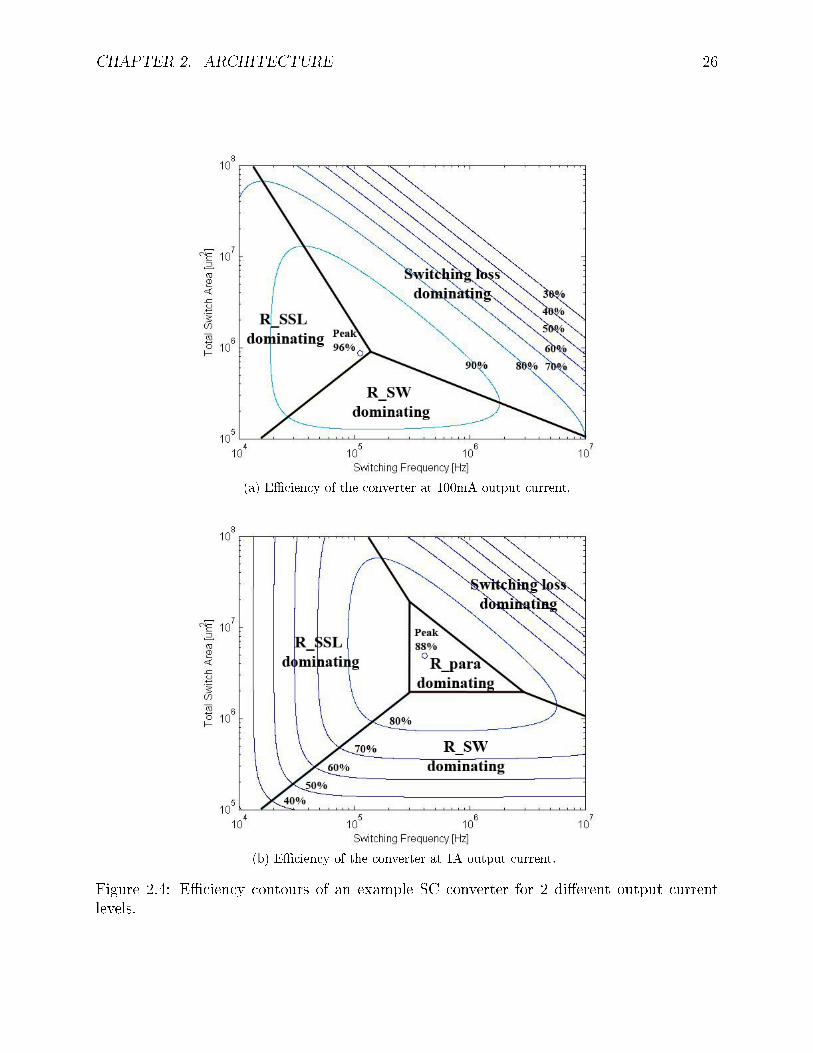
CHAPTER 2. ARCHITECTURE 26
(a) Eciency of the converter at 100mA output current.
(b) Eciency of the converter at 1A output current.
Figure 2.4: Eciency contours of an example SC converter for 2 dierent output currentlevels.
CHAPTER 2. ARCHITECTURE 27
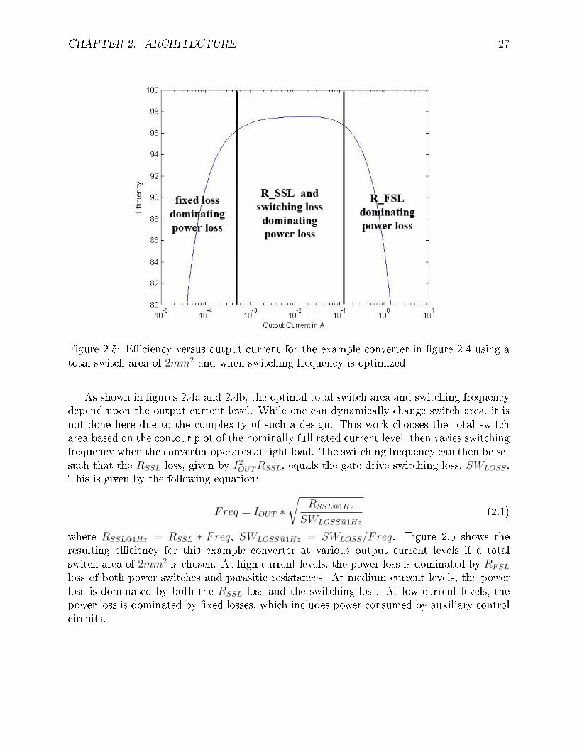
Figure 2.5: Eciency versus output current for the example converter in gure 2.4 using atotal switch area of 2mm2 and when switching frequency is optimized.
As shown in gures 2.4a and 2.4b, the optimal total switch area and switching frequencydepend upon the output current level. While one can dynamically change switch area, it isnot done here due to the complexity of such a design. This work chooses the total switcharea based on the contour plot of the nominally full rated current level, then varies switchingfrequency when the converter operates at light load. The switching frequency can then be setsuch that the RSSL loss, given by I2OUTRSSL, equals the gate drive switching loss, SWLOSS.This is given by the following equation:
Freq = IOUT ∗√
RSSL@1Hz
SWLOSS@1Hz
(2.1)
where RSSL@1Hz = RSSL ∗ Freq, SWLOSS@1Hz = SWLOSS/Freq. Figure 2.5 shows theresulting eciency for this example converter at various output current levels if a totalswitch area of 2mm2 is chosen. At high current levels, the power loss is dominated by RFSL
loss of both power switches and parasitic resistances. At medium current levels, the powerloss is dominated by both the RSSL loss and the switching loss. At low current levels, thepower loss is dominated by xed losses, which includes power consumed by auxiliary controlcircuits.
CHAPTER 2. ARCHITECTURE 28
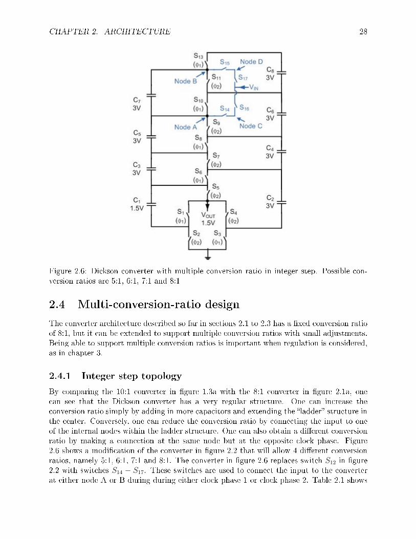
Figure 2.6: Dickson converter with multiple conversion ratio in integer step. Possible con-version ratios are 5:1, 6:1, 7:1 and 8:1
2.4 Multi-conversion-ratio design
The converter architecture described so far in sections 2.1 to 2.3 has a xed conversion ratioof 8:1, but it can be extended to support multiple conversion ratios with small adjustments.Being able to support multiple conversion ratios is important when regulation is considered,as in chapter 3.
2.4.1 Integer step topology
By comparing the 10:1 converter in gure 1.3a with the 8:1 converter in gure 2.1a, onecan see that the Dickson converter has a very regular structure. One can increase theconversion ratio simply by adding in more capacitors and extending the ladder structure inthe center. Conversely, one can reduce the conversion ratio by connecting the input to oneof the internal nodes within the ladder structure. One can also obtain a dierent conversionratio by making a connection at the same node but at the opposite clock phase. Figure2.6 shows a modication of the converter in gure 2.2 that will allow 4 dierent conversionratios, namely 5:1, 6:1, 7:1 and 8:1. The converter in gure 2.6 replaces switch S12 in gure2.2 with switches S14 − S17. These switches are used to connect the input to the converterat either node A or B during during either clock phase 1 or clock phase 2. Table 2.1 shows
CHAPTER 2. ARCHITECTURE 29
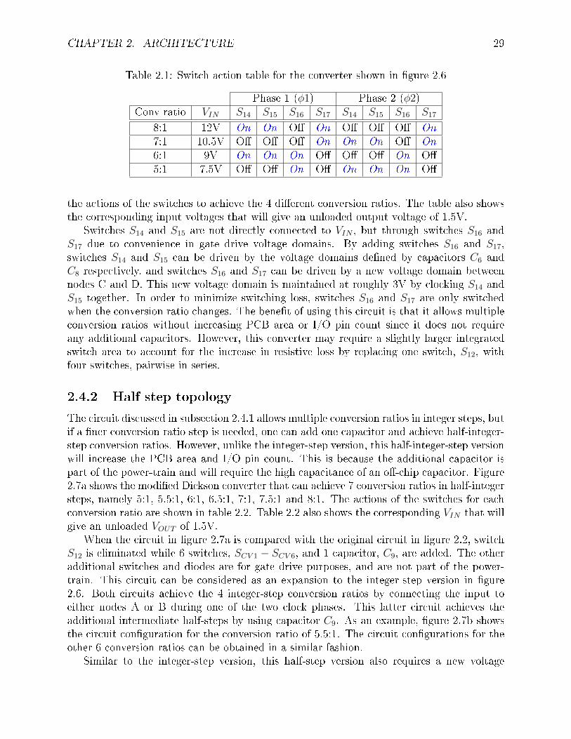
Table 2.1: Switch action table for the converter shown in gure 2.6
Phase 1 (φ1) Phase 2 (φ2)Conv ratio VIN S14 S15 S16 S17 S14 S15 S16 S17
8:1 12V On On O On O O O On7:1 10.5V O O O On On On O On6:1 9V On On On O O O On O5:1 7.5V O O On O On On On O
the actions of the switches to achieve the 4 dierent conversion ratios. The table also showsthe corresponding input voltages that will give an unloaded output voltage of 1.5V.
Switches S14 and S15 are not directly connected to VIN , but through switches S16 andS17 due to convenience in gate drive voltage domains. By adding switches S16 and S17,switches S14 and S15 can be driven by the voltage domains dened by capacitors C6 andC8 respectively, and switches S16 and S17 can be driven by a new voltage domain betweennodes C and D. This new voltage domain is maintained at roughly 3V by clocking S14 andS15 together. In order to minimize switching loss, switches S16 and S17 are only switchedwhen the conversion ratio changes. The benet of using this circuit is that it allows multipleconversion ratios without increasing PCB area or I/O pin count since it does not requireany additional capacitors. However, this converter may require a slightly larger integratedswitch area to account for the increase in resistive loss by replacing one switch, S12, withfour switches, pairwise in series.
2.4.2 Half step topology
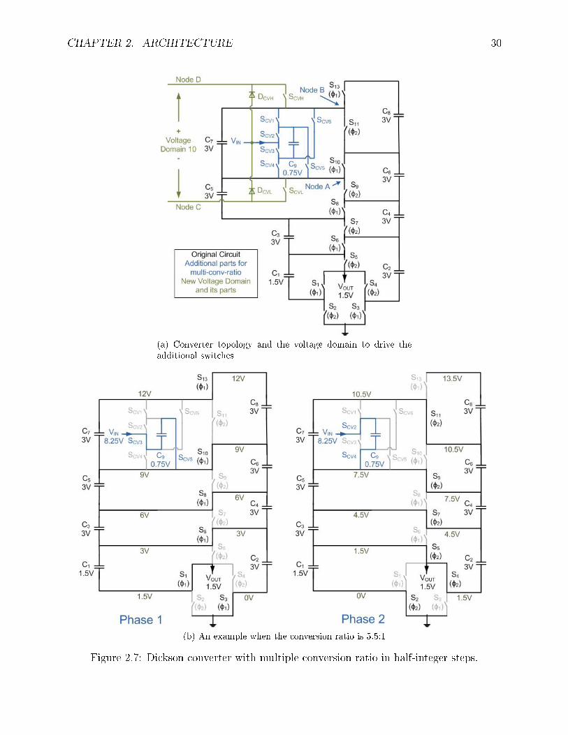
The circuit discussed in subsection 2.4.1 allows multiple conversion ratios in integer steps, butif a ner conversion ratio step is needed, one can add one capacitor and achieve half-integer-step conversion ratios. However, unlike the integer-step version, this half-integer-step versionwill increase the PCB area and I/O pin count. This is because the additional capacitor ispart of the power-train and will require the high capacitance of an o-chip capacitor. Figure2.7a shows the modied Dickson converter that can achieve 7 conversion ratios in half-integersteps, namely 5:1, 5.5:1, 6:1, 6.5:1, 7:1, 7.5:1 and 8:1. The actions of the switches for eachconversion ratio are shown in table 2.2. Table 2.2 also shows the corresponding VIN that willgive an unloaded VOUT of 1.5V.
When the circuit in gure 2.7a is compared with the original circuit in gure 2.2, switchS12 is eliminated while 6 switches, SCV 1 − SCV 6, and 1 capacitor, C9, are added. The otheradditional switches and diodes are for gate drive purposes, and are not part of the power-train. This circuit can be considered as an expansion to the integer-step version in gure2.6. Both circuits achieve the 4 integer-step conversion ratios by connecting the input toeither nodes A or B during one of the two clock phases. This latter circuit achieves theadditional intermediate half-steps by using capacitor C9. As an example, gure 2.7b showsthe circuit conguration for the conversion ratio of 5.5:1. The circuit congurations for theother 6 conversion ratios can be obtained in a similar fashion.
Similar to the integer-step version, this half-step version also requires a new voltage
CHAPTER 2. ARCHITECTURE 30
(a) Converter topology and the voltage domain to drive theadditional switches
(b) An example when the conversion ratio is 5.5:1
Figure 2.7: Dickson converter with multiple conversion ratio in half-integer steps.

CHAPTER 2. ARCHITECTURE 31
Table 2.2: Switch action table for the circuit in gure 2.7 . Parameter n stands for conversionratio.
Phase 1 (φ1)n VIN SCV 1 SCV 2 SCV 3 SCV 4 SCV 5 SCV 6 SCV H DCV H SCV L DCV L
8:1 12V On On O O O O On O On O7.5:1 11.25V On O On O O O On O On O7:1 10.5V O O O O O O On O On O6.5:1 9.75V O On O On O O On O On O6:1 9V O O On On O O On O On O5.5:1 8.25V O O On O On O On O O On5:1 7.5V O O O O O O On O O On
Phase 2 (φ2)n VIN SCV 1 SCV 2 SCV 3 SCV 4 SCV 5 SCV 6 SCV H DCV H SCV L DCV L
8:1 12V O O O O O O O On On O7.5:1 11.25V O On O O O On O On On O7:1 10.5V On On O O O O On O On O6.5:1 9.75V On O On O O O On O On O6:1 9V O O O O O O On O On O5.5:1 8.25V O On O On O O On O On O5:1 7.5V O O On On O O On O On O

CHAPTER 2. ARCHITECTURE 32
domain to drive the additional switches. The rails that dene this new voltage domain arenamed nodes C and D in gure 2.7a as in the integer-step version in gure 2.6. However, thisnew voltage domain is more complicated than any of the other voltage domains discussed sofar. This voltage domain does not have a xed voltage level, but changes with clock phaseand conversion ratio. The voltage level varies from 3V to 4.5V, but it is within the 5V ratedvoltage of the 0.6µm transistor available in this process. Switches SCV H and SCV L, anddiodes DCV H and DCV L are used to control this voltage domain, and their actions are alsoshown in table 2.2. Switch SCV L and diode DCV L are used to connect node C to either VINor node A, whichever has a lower voltage level. Similarly, switch SCV H and diode DCV H areused to connect node D to either VIN or node B, whichever has a higher voltage level.
2.5 Shutdown and Startup
As discussed in section 2.2, dividing the converter into multiple voltage domains allows theusage of 1.8V and 5V transistors in this 12V converter. These voltage domains are denedby the power-train capacitors, which during normal operation, have near constant voltagelevels due to the switching action of the converter. However, these voltage levels are notwell dened during the transients of shutdown and startup, and a protection scheme and astartup plan is needed.
2.5.1 Shutdown protection
After a converter stops switching during shutdown, the power-train capacitor voltages maydrift in an unanticipated manner and cause over-voltage levels in some voltage domains.To prevent this from happening and over-stressing any device, active clamp circuits areimplemented in each voltage domain to limit the peak voltage level. Figure 2.8 shows theconceptual idea of this clamp; the circuit details are discussed in section 4.2. The voltagelevel of the voltage domain is divided down by a resistive divider, and then compared to areference voltage. If the voltage level is too high, the comparator will turn on an NMOStransistor, drain current across the voltage domain and reduce the voltage back to a safelevel. Since capacitor voltage drift is a slow process, this clamp circuit has a low bandwidthand consumes little power. This clamp circuit is designed to drain 5mA when on, and about200nA when o. The power consumed by these clamps is less than the power loss due tosub-threshold leakage current through the power-train switches.
2.5.2 Startup scheme
The objective of the startup scheme is to charge up the power-train capacitors and buildup the various voltage domains while protecting the low-voltage transistors from the highvoltage input source during this transient. Figure 2.9 shows the concept of the startupscheme implemented in this work. Initially, the converter is isolated from the input sourcewith a high voltage blocking switch while a precharging regulator charges up the output rail.The converter then operates in charge-pump (boost) mode to charge up all the capacitorsand internal nodes to pre-determined values. The high voltage blocking switch is then
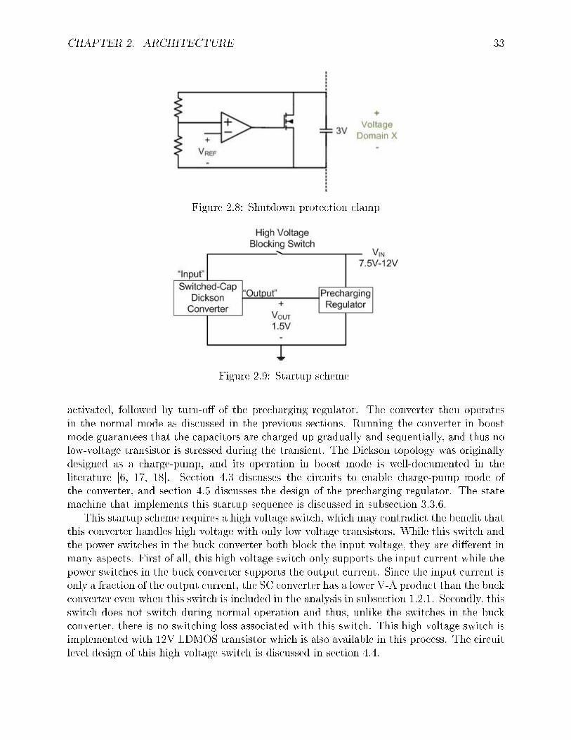
CHAPTER 2. ARCHITECTURE 33
Figure 2.8: Shutdown protection clamp
Figure 2.9: Startup scheme
activated, followed by turn-o of the precharging regulator. The converter then operatesin the normal mode as discussed in the previous sections. Running the converter in boostmode guarantees that the capacitors are charged up gradually and sequentially, and thus nolow-voltage transistor is stressed during the transient. The Dickson topology was originallydesigned as a charge-pump, and its operation in boost mode is well-documented in theliterature [6, 17, 18]. Section 4.3 discusses the circuits to enable charge-pump mode ofthe converter, and section 4.5 discusses the design of the precharging regulator. The statemachine that implements this startup sequence is discussed in subsection 3.3.6.
This startup scheme requires a high voltage switch, which may contradict the benet thatthis converter handles high voltage with only low voltage transistors. While this switch andthe power switches in the buck converter both block the input voltage, they are dierent inmany aspects. First of all, this high voltage switch only supports the input current while thepower switches in the buck converter supports the output current. Since the input current isonly a fraction of the output current, the SC converter has a lower V-A product than the buckconverter even when this switch is included in the analysis in subsection 1.2.1. Secondly, thisswitch does not switch during normal operation and thus, unlike the switches in the buckconverter, there is no switching loss associated with this switch. This high voltage switch isimplemented with 12V LDMOS transistor which is also available in this process. The circuitlevel design of this high voltage switch is discussed in section 4.4.
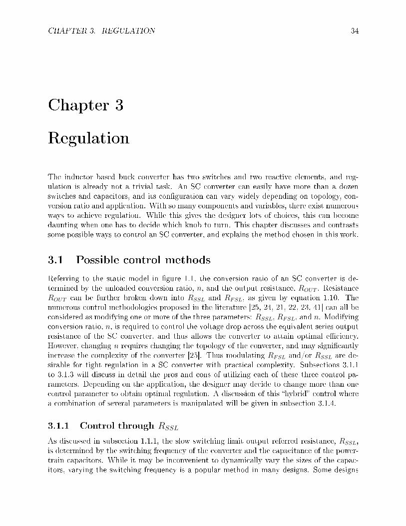
CHAPTER 3. REGULATION 34
Chapter 3
Regulation
The inductor based buck converter has two switches and two reactive elements, and reg-ulation is already not a trivial task. An SC converter can easily have more than a dozenswitches and capacitors, and its conguration can vary widely depending on topology, con-version ratio and application. With so many components and variables, there exist numerousways to achieve regulation. While this gives the designer lots of choices, this can becomedaunting when one has to decide which knob to turn. This chapter discusses and contrastssome possible ways to control an SC converter, and explains the method chosen in this work.
3.1 Possible control methods
Referring to the static model in gure 1.1, the conversion ratio of an SC converter is de-termined by the unloaded conversion ratio, n, and the output resistance, ROUT . ResistanceROUT can be further broken down into RSSL and RFSL, as given by equation 1.10. Thenumerous control methodologies proposed in the literature [25, 24, 21, 22, 23, 41] can all beconsidered as modifying one or more of the three parameters: RSSL, RFSL, and n. Modifyingconversion ratio, n, is required to control the voltage drop across the equivalent series outputresistance of the SC converter, and thus allows the converter to attain optimal eciency.However, changing n requires changing the topology of the converter, and may signicantlyincrease the complexity of the converter [25]. Thus modulating RFSL and/or RSSL are de-sirable for tight regulation in a SC converter with practical complexity. Subsections 3.1.1to 3.1.3 will discuss in detail the pros and cons of utilizing each of these three control pa-rameters. Depending on the application, the designer may decide to change more than onecontrol parameter to obtain optimal regulation. A discussion of this hybrid control wherea combination of several parameters is manipulated will be given in subsection 3.1.4.
3.1.1 Control through RSSL
As discussed in subsection 1.1.1, the slow switching limit output referred resistance, RSSL,is determined by the switching frequency of the converter and the capacitance of the power-train capacitors. While it may be inconvenient to dynamically vary the sizes of the capac-itors, varying the switching frequency is a popular method in many designs. Some designs
CHAPTER 3. REGULATION 35
skip clock pulses [21], and some designs control the clock hysteretically [22]. While thesemethods dier in implementations, they all achieve regulation through eectively varyingthe switching frequency of a converter.
The main advantage of using switching frequency to achieve regulation is high eciencyat light load conditions. As load current reduces, switching frequency is reduced to maintainregulation. This in turns reduces switching loss, which is usually the dominant loss factorat light load conditions. Further, many frequency regulators consume low standby poweras they are made up of only comparators and digital logic. As discussed in subsection2.3.3, this allows high eciency at very light loads when the converter is barely switchingand standby power dominates power loss. The main disadvantages of controlling throughswitching frequency is potentially high output voltage ripple as charge transfer is impulsivein the SSL. In order to compensate for this, a large output capacitor CL may be required orinterleaving has to be introduced [26]. This will, however, increase component cost or thecomplexity of the controller, in the case of o-chip capacitors.
3.1.2 Control through RFSL
Instead of varying RSSL, one can control ROUT by varying the RFSL term in equation 1.10.This either involves changing the duty ratio of the switches [24], or the resistances of theswitches by controlling gate-drive voltage [23], or switch size. If the control methodologyinvolves changing the resistances of the switches connected to the output terminal, currentto the output can be held at near constant values, and the output voltage ripple can beminimized [41]. With this control method, the SC converter will behave very similarlyto a linear regulator, and the compensation techniques developed for the linear regulators[20] are excellent references. However, there are additional dynamics associated with theSC converter that are absent in the linear regulator, and these dynamics have to be wellunderstood if aggressive compensation schemes such as canceling of poles and zeros areused.
The main drawback of varying RFSL to control VOUT is reduced eciency at light loadif switching frequency is constant at all times. Eciency is also reduced in heavy load asoperating in the FSL requires high switching frequency, which increases switching loss. Ifswitch resistance control is being used, further losses from high standby power may be in-curred. This is because controlling switch gate-drive voltage requires analog buers, whichare more power hungry than their digital counterparts. Duty ratio control eliminates theanalog buer but may not support regulation for a wide load range. To maintain regulation,duty ratio is proportional to load current. While load current may vary by orders of magni-tude, varying duty ratio by orders of magnitude is impractical, or at least dicult or costly.All of these disadvantages can be mitigated by dynamically reducing the switch sizes at lowcurrent levels. This will, however, increase the complexity of the controller and the controlalgorithm.
3.1.3 Control through conversion ratio, n
While regulation can be achieved through varying the output resistance of the converter, thisrequires a voltage drop across a resistive element and thus limits the maximum eciency
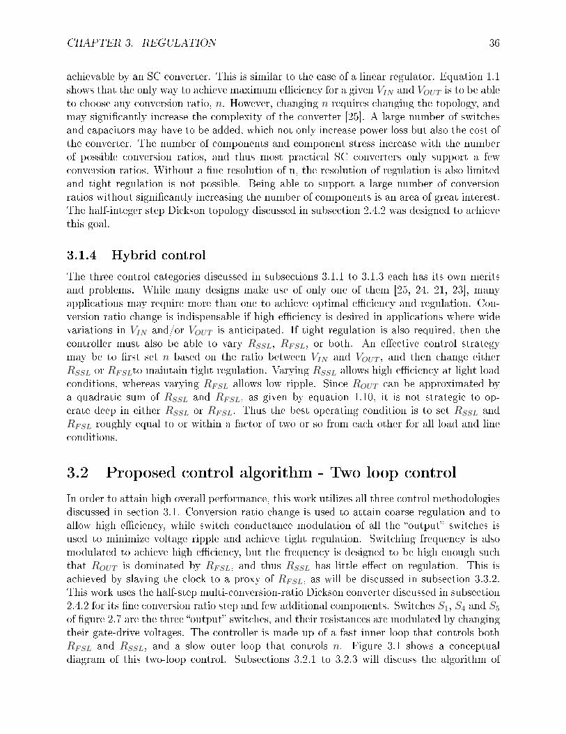
CHAPTER 3. REGULATION 36
achievable by an SC converter. This is similar to the case of a linear regulator. Equation 1.1shows that the only way to achieve maximum eciency for a given VIN and VOUT is to be ableto choose any conversion ratio, n. However, changing n requires changing the topology, andmay signicantly increase the complexity of the converter [25]. A large number of switchesand capacitors may have to be added, which not only increase power loss but also the cost ofthe converter. The number of components and component stress increase with the numberof possible conversion ratios, and thus most practical SC converters only support a fewconversion ratios. Without a ne resolution of n, the resolution of regulation is also limitedand tight regulation is not possible. Being able to support a large number of conversionratios without signicantly increasing the number of components is an area of great interest.The half-integer step Dickson topology discussed in subsection 2.4.2 was designed to achievethis goal.
3.1.4 Hybrid control
The three control categories discussed in subsections 3.1.1 to 3.1.3 each has its own meritsand problems. While many designs make use of only one of them [25, 24, 21, 23], manyapplications may require more than one to achieve optimal eciency and regulation. Con-version ratio change is indispensable if high eciency is desired in applications where widevariations in VIN and/or VOUT is anticipated. If tight regulation is also required, then thecontroller must also be able to vary RSSL, RFSL, or both. An eective control strategymay be to rst set n based on the ratio between VIN and VOUT , and then change eitherRSSL or RFSLto maintain tight regulation. Varying RSSL allows high eciency at light loadconditions, whereas varying RFSL allows low ripple. Since ROUT can be approximated bya quadratic sum of RSSL and RFSL, as given by equation 1.10, it is not strategic to op-erate deep in either RSSL or RFSL. Thus the best operating condition is to set RSSL andRFSL roughly equal to or within a factor of two or so from each other for all load and lineconditions.
3.2 Proposed control algorithm - Two loop control
In order to attain high overall performance, this work utilizes all three control methodologiesdiscussed in section 3.1. Conversion ratio change is used to attain coarse regulation and toallow high eciency, while switch conductance modulation of all the output switches isused to minimize voltage ripple and achieve tight regulation. Switching frequency is alsomodulated to achieve high eciency, but the frequency is designed to be high enough suchthat ROUT is dominated by RFSL, and thus RSSL has little eect on regulation. This isachieved by slaving the clock to a proxy of RFSL, as will be discussed in subsection 3.3.2.This work uses the half-step multi-conversion-ratio Dickson converter discussed in subsection2.4.2 for its ne conversion ratio step and few additional components. Switches S1, S4 and S5
of gure 2.7 are the three output switches, and their resistances are modulated by changingtheir gate-drive voltages. The controller is made up of a fast inner loop that controls bothRFSL and RSSL, and a slow outer loop that controls n. Figure 3.1 shows a conceptualdiagram of this two-loop control. Subsections 3.2.1 to 3.2.3 will discuss the algorithm of
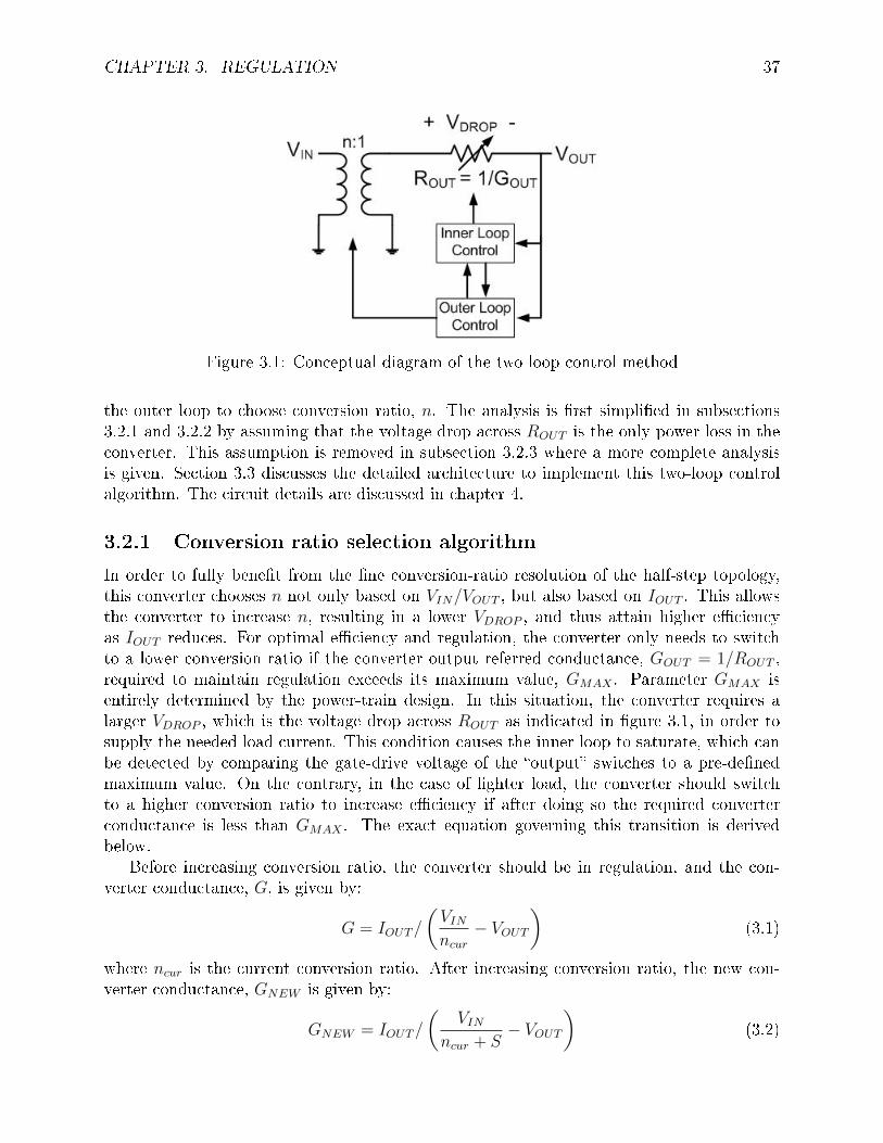
CHAPTER 3. REGULATION 37
Figure 3.1: Conceptual diagram of the two loop control method
the outer loop to choose conversion ratio, n. The analysis is rst simplied in subsections3.2.1 and 3.2.2 by assuming that the voltage drop across ROUT is the only power loss in theconverter. This assumption is removed in subsection 3.2.3 where a more complete analysisis given. Section 3.3 discusses the detailed architecture to implement this two-loop controlalgorithm. The circuit details are discussed in chapter 4.
3.2.1 Conversion ratio selection algorithm
In order to fully benet from the ne conversion-ratio resolution of the half-step topology,this converter chooses n not only based on VIN/VOUT , but also based on IOUT . This allowsthe converter to increase n, resulting in a lower VDROP , and thus attain higher eciencyas IOUT reduces. For optimal eciency and regulation, the converter only needs to switchto a lower conversion ratio if the converter output referred conductance, GOUT = 1/ROUT ,required to maintain regulation exceeds its maximum value, GMAX . Parameter GMAX isentirely determined by the power-train design. In this situation, the converter requires alarger VDROP , which is the voltage drop across ROUT as indicated in gure 3.1, in order tosupply the needed load current. This condition causes the inner loop to saturate, which canbe detected by comparing the gate-drive voltage of the output switches to a pre-denedmaximum value. On the contrary, in the case of lighter load, the converter should switchto a higher conversion ratio to increase eciency if after doing so the required converterconductance is less than GMAX . The exact equation governing this transition is derivedbelow.
Before increasing conversion ratio, the converter should be in regulation, and the con-verter conductance, G, is given by:
G = IOUT/
(VINncur
− VOUT)
(3.1)
where ncur is the current conversion ratio. After increasing conversion ratio, the new con-verter conductance, GNEW is given by:
GNEW = IOUT/
(VIN
ncur + S− VOUT
)(3.2)
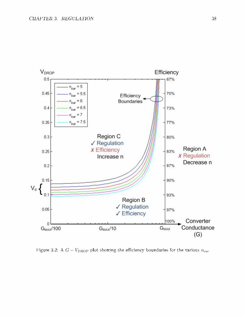
CHAPTER 3. REGULATION 38
Figure 3.2: A G− VDROP plot showing the eciency boundaries for the various ncur
CHAPTER 3. REGULATION 39
where ncur + S is the new conversion ratio, and S is the step size in n. Parameter S equals0.5 for the half-step converter in subsection 2.4.2, and equals 1 for the integer-step converterin subsection 2.4.1. If GNEW < GMAX , then the converter should increase conversion ratio.By combining equations 3.1 and 3.2, and the inequality GNEW < GMAX , this condition isgiven by:
G < GMAX
(VIN
ncur+S− VOUT
)(VINncur− VOUT
) (3.3)
which can also be rewritten as:
G < GMAXVDROP − VdVDROP
(3.4)
VDROP =VINncur
− VOUT (3.5)
Vd =VINncur
− VINncur + S
=S (VDROP + VOUT )
ncur + S(3.6)
where Vd is the value of VDROP under open circuit condition, G = 0, and it representsthe minimum VDROP before an increase in conversion ratio should be considered. Pluggingin the values for this converter, VOUT = 1.5V , S = 0.5, 5 < ncur < 7.5, and assumingVOUT VDROP , Vd ranges from 0.094V to 0.136V. Conversion ratio ncur = 8 is not consideredbecause it is the highest conversion ratio possible, and thus the converter cannot switch toyet a higher one.
Figure 3.2 shows equation 3.4 on the G − VDROP plane. Equation 3.4, together withG = GMAX , divides the G − VDROP plane into three regions, characterized by whetherregulation is satised and whether maximum eciency is obtained. In region A, regulationis not satised since it requires a conduction, G, beyond its maximum value, GMAX . Inregion C, regulation is satised but eciency is not maximized since inequality 3.4 holdshere. It is only in region B that both regulation and maximum eciency are satised. Sinceinequality 3.4 separates region B from region C where the dierence is achieving maximumeciency, it is labeled as an eciency boundary. In gure 3.2, eciency boundaries areshown for the seven dierent values of current conversion ratio, ncur.
Figure 3.2 represents the control algorithm developed in this work, and it governs whenconversion ratio should be changed. If the controller were to command the converter tooperate in region A, where G > GMAX , the converter would go out of regulation, andit needs to decrease conversion ratio. If the converter is operating in region C, G is onthe left of the eciency boundary, and inequality 3.4 is satised. The converter is underregulation, but can and should maximize eciency by increasing conversion ratio. In regionB, the converter is both under regulation and at the maximum eciency achievable by theconverter. With this scheme, there is one and only one conversion ratio that lies withinregion B for any VIN and IOUT pair.
As shown in gure 3.2, the eciency boundary depends on ncur. In order to simplify thecontrol algorithm, this work uses the eciency boundary corresponding to ncur = 5 regardlessof the actual ncur. This leads to more than one possible conversion ratio that lies within region
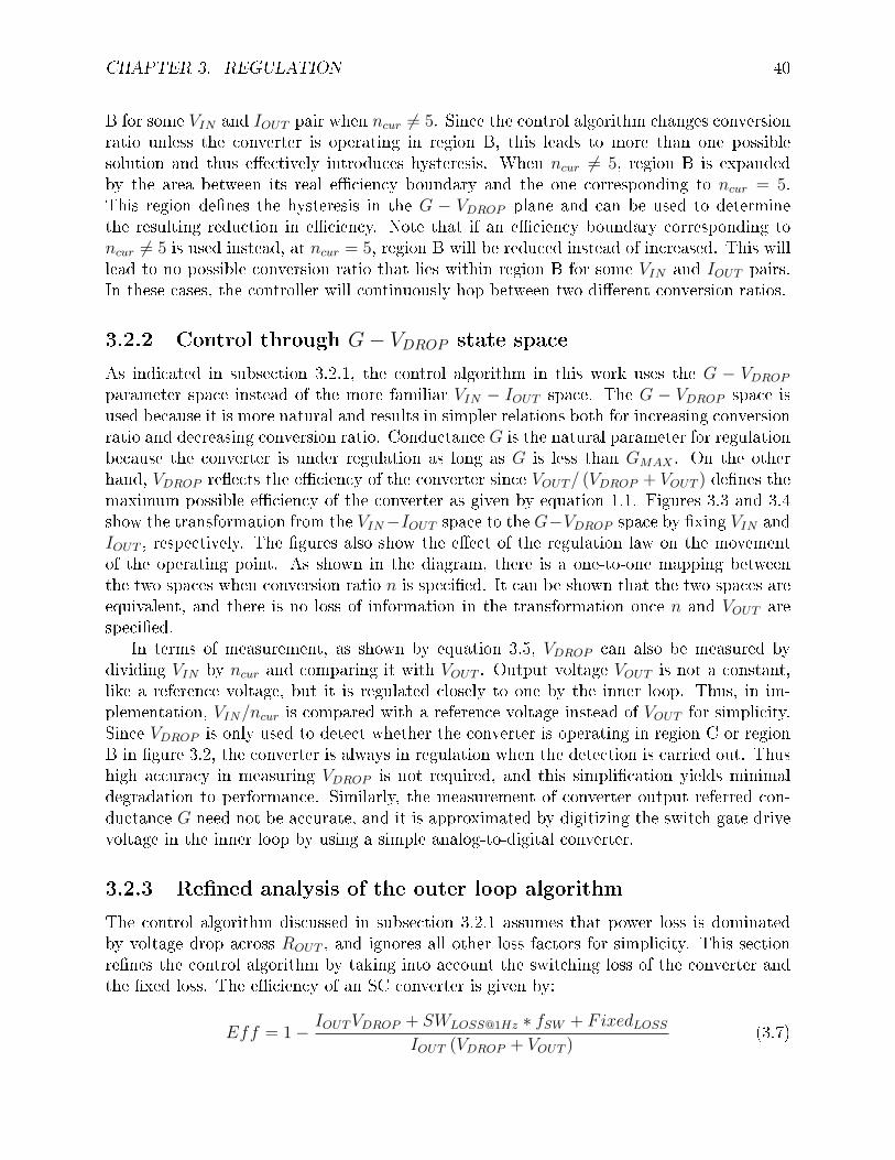
CHAPTER 3. REGULATION 40
B for some VIN and IOUT pair when ncur 6= 5. Since the control algorithm changes conversionratio unless the converter is operating in region B, this leads to more than one possiblesolution and thus eectively introduces hysteresis. When ncur 6= 5, region B is expandedby the area between its real eciency boundary and the one corresponding to ncur = 5.This region denes the hysteresis in the G − VDROP plane and can be used to determinethe resulting reduction in eciency. Note that if an eciency boundary corresponding toncur 6= 5 is used instead, at ncur = 5, region B will be reduced instead of increased. This willlead to no possible conversion ratio that lies within region B for some VIN and IOUT pairs.In these cases, the controller will continuously hop between two dierent conversion ratios.
3.2.2 Control through G− VDROP state space
As indicated in subsection 3.2.1, the control algorithm in this work uses the G − VDROPparameter space instead of the more familiar VIN − IOUT space. The G − VDROP space isused because it is more natural and results in simpler relations both for increasing conversionratio and decreasing conversion ratio. Conductance G is the natural parameter for regulationbecause the converter is under regulation as long as G is less than GMAX . On the otherhand, VDROP reects the eciency of the converter since VOUT/ (VDROP + VOUT ) denes themaximum possible eciency of the converter as given by equation 1.1. Figures 3.3 and 3.4show the transformation from the VIN−IOUT space to the G−VDROP space by xing VIN andIOUT , respectively. The gures also show the eect of the regulation law on the movementof the operating point. As shown in the diagram, there is a one-to-one mapping betweenthe two spaces when conversion ratio n is specied. It can be shown that the two spaces areequivalent, and there is no loss of information in the transformation once n and VOUT arespecied.
In terms of measurement, as shown by equation 3.5, VDROP can also be measured bydividing VIN by ncur and comparing it with VOUT . Output voltage VOUT is not a constant,like a reference voltage, but it is regulated closely to one by the inner loop. Thus, in im-plementation, VIN/ncur is compared with a reference voltage instead of VOUT for simplicity.Since VDROP is only used to detect whether the converter is operating in region C or regionB in gure 3.2, the converter is always in regulation when the detection is carried out. Thushigh accuracy in measuring VDROP is not required, and this simplication yields minimaldegradation to performance. Similarly, the measurement of converter output referred con-ductance G need not be accurate, and it is approximated by digitizing the switch gate drivevoltage in the inner loop by using a simple analog-to-digital converter.
3.2.3 Rened analysis of the outer loop algorithm
The control algorithm discussed in subsection 3.2.1 assumes that power loss is dominatedby voltage drop across ROUT , and ignores all other loss factors for simplicity. This sectionrenes the control algorithm by taking into account the switching loss of the converter andthe xed loss. The eciency of an SC converter is given by:
Eff = 1− IOUTVDROP + SWLOSS@1Hz ∗ fSW + FixedLOSSIOUT (VDROP + VOUT )
(3.7)
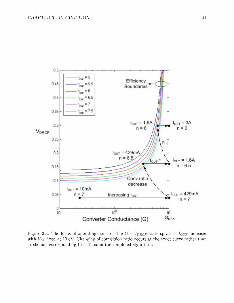
CHAPTER 3. REGULATION 41
Figure 3.3: The locus of operating point on the G − VDROP state space as IOUT increaseswith VIN xed at 10.8V. Changing of conversion ratio occurs at the exact curve rather thanat the one corresponding to n=5, as in the simplied algorithm.
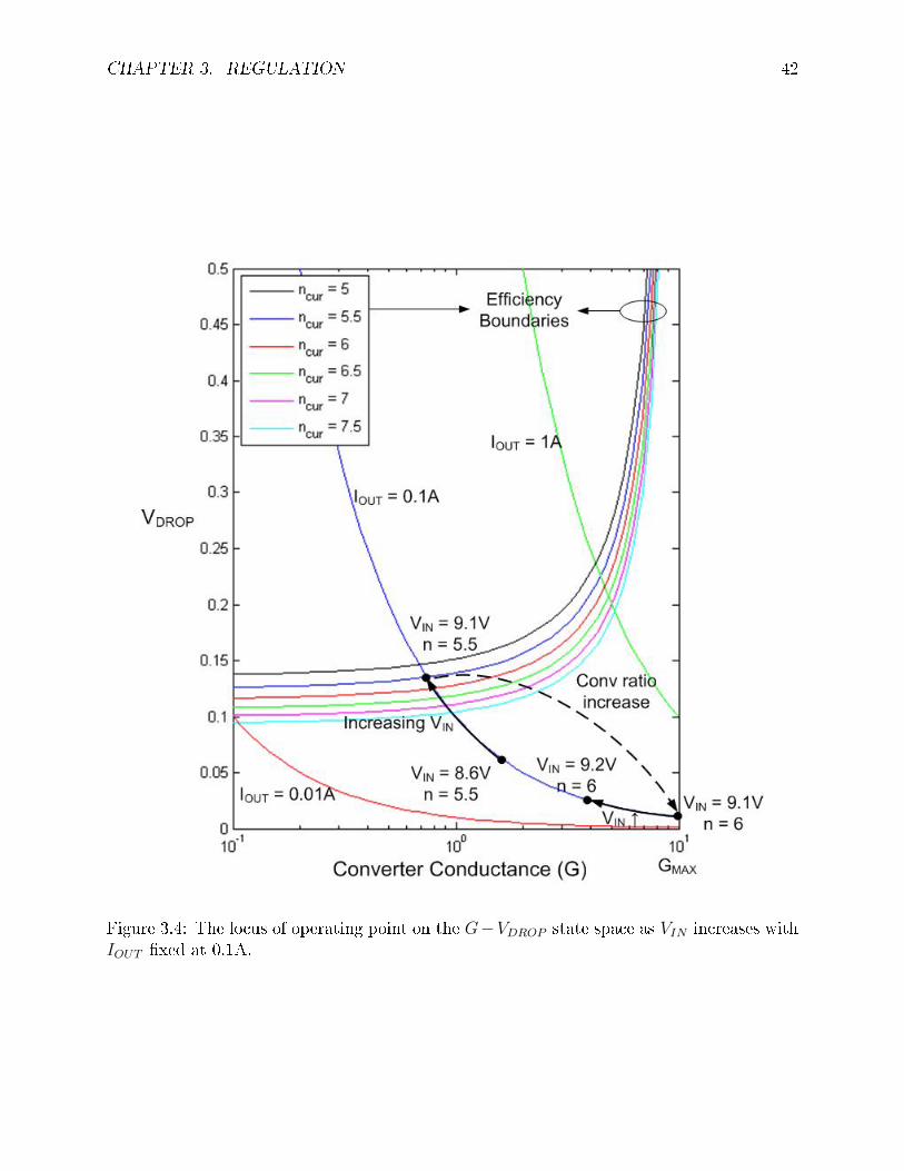
CHAPTER 3. REGULATION 42
Figure 3.4: The locus of operating point on the G−VDROP state space as VIN increases withIOUT xed at 0.1A.
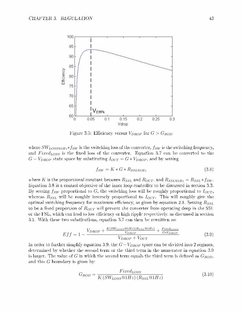
CHAPTER 3. REGULATION 43
Figure 3.5: Eciency versus VDROP for G > GBOD
where SWLOSS@1Hz∗fSW is the switching loss of the converter, fSW is the switching frequency,and FixedLOSS is the xed loss of the converter. Equation 3.7 can be converted to theG− VDROP state space by substituting IOUT = G ∗ VDROP , and by setting
fSW = K ∗G ∗RSSL@1Hz (3.8)
where K is the proportional constant between RSSL and ROUT , and RSSL@1Hz = RSSL∗fSW .Equation 3.8 is a control objective of the inner loop controller to be discussed in section 3.3.By setting fSW proportional to G, the switching loss will be roughly proportional to IOUT ,whereas RSSL will be roughly inversely proportional to IOUT . This will roughly give theoptimal switching frequency for maximum eciency, as given by equation 2.1. Setting RSSL
to be a xed proportion of ROUT will prevent the converter from operating deep in the SSLor the FSL, which can lead to low eciency or high ripple respectively, as discussed in section3.1. With these two substitutions, equation 3.7 can then be rewritten as:
Eff = 1−VDROP + K(SWLOSS@1Hz)(RSSL@1Hz)
VDROP+ FixedLOSS
G∗VDROP
VDROP + VOUT(3.9)
In order to further simplify equation 3.9, the G−VDROP space can be divided into 2 regimes,determined by whether the second term or the third term in the numerator in equation 3.9is larger. The value of G in which the second term equals the third term is dened as GBOD,and this G boundary is given by:
GBOD =FixedLOSS
K (SWLOSS@1Hz) (RSSL@1Hz)(3.10)
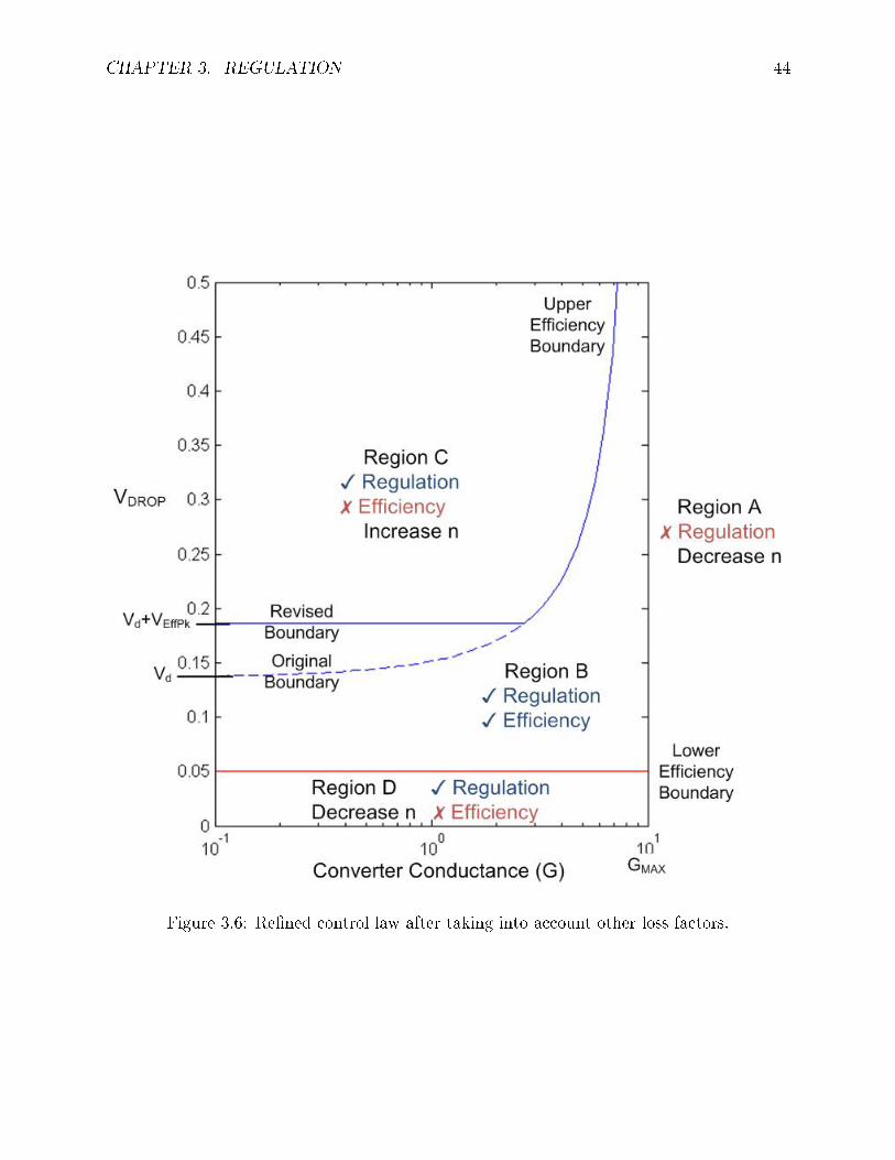
CHAPTER 3. REGULATION 44
Figure 3.6: Rened control law after taking into account other loss factors.
CHAPTER 3. REGULATION 45
When the second term of the numerator in equation 3.9 is larger than the third term, thatis G < GBOD, the power loss of the converter is dominated by leakage power and the constantpower drawn by the control circuitry. During this situation, load current is very low and theconverter is basically sitting idle. As discussed in chapter 2 subsection 2.3.3 and shown bygure 2.5, eciency in this operating region drops very quickly with falling load regardlessof control action. In this region, the controller has little leeway to increase eciency besidesturning itself o. To avoid the additional complexity of powering on and o the controller,this work focuses on situations where control action can make a dierence. While thereis little benet in doing optimal control when G < GBOD, the controller can potentiallyincrease peak eciency signicantly when G > GBOD. The controller can make an impactby choosing the optimal conversion ratio to trade-o the rst term and second term of thenumerator in equation 3.9. Thus this discussion focuses on the case when G > GBOD, andthe third term in equation 3.9 will be ignored.
With this simplication of equation 3.9, it can be shown that eciency peaks at VDROP =VEffPk where VEffPk is given by:
VEffPk =√K (SWLOSS@1Hz) (RSSL@1Hz) (3.11)
Figure 3.5 shows eciency versus VDROP as predicted by equation 3.9 when G GBOD.As shown in the gure, eciency peaks at VDROP = VEffPk, but reduces sharply as VDROPapproaches zero. Thus in order to obtain maximum eciency, the converter should reduceconversion ratio and increase VDROP at low VDROP values. This denes an eciency boundaryin addition to the one dened by inequality 3.4. When VDROP falls below this additionaleciency boundary, the converter should reduce conversion ratio. This additional eciencyboundary will be denoted as the lower eciency boundary since it occurs at low VDROPvalues, whereas the one dened by equation 3.4 will be called the upper eciency boundary.
Finding an algebraic expression for this lower eciency boundary can be tricky anddicult to implement. In order to simplify the control low, this work picks the lower eciencyboundary to be a xed VDROP value, and this value is chosen to be the VEffPk at G =GMAX . This choice sets the lower eciency boundary to be closer to VDROP > VEffPk,and due to the asymmetrical steepness from the two side of the peak in gure 3.5, this willreduce the impact on eciency of such a simplication. This lower eciency boundary isimplemented by adding one more control constraint to the control law discussed in subsection3.2.1. This rened control law is shown in gure 3.6. Instead of decreasing conversionratio only when G > GMAX , the control law now decreases conversion ratio when eitherG > GMAX or VDROP < VEffPk@ (G = GMAX) is satised. For increasing conversion ratio,the controller needs to check both the condition dened by inequality 3.4 and VDROP >Vd + VEffPk@ (G = GMAX). This additional condition prevents the converter from fallinginto region D when conversion ratio is increased. If this were to occur, the converter wouldkeep hopping between two conversion ratios.
3.3 Controller implementation
Figure 3.7 shows the block diagram of the controller implemented in this work. As discussedin section 3.2, the controller is divided into two loops; the inner loop modulates the switch
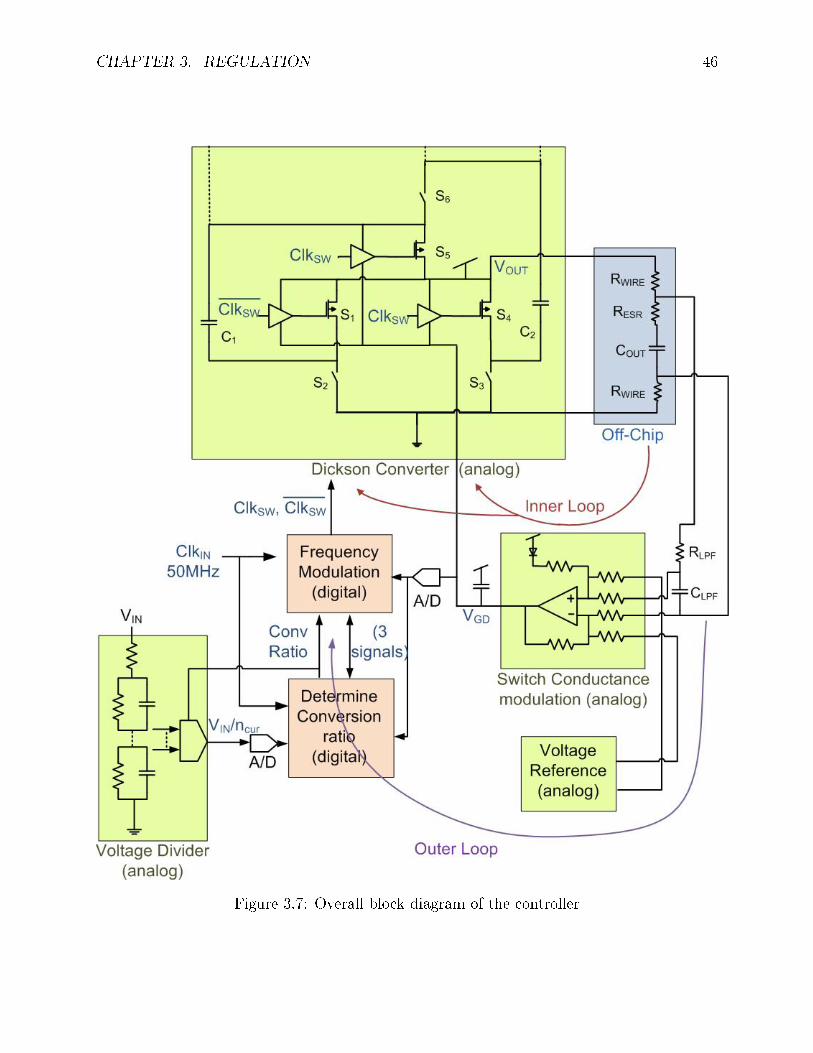
CHAPTER 3. REGULATION 46
Figure 3.7: Overall block diagram of the controller
CHAPTER 3. REGULATION 47
conductance and switching frequency, and the outer loop modulates the conversion ratio,n. Switch conductance modulation is achieved through modulating the gate drive voltagesof the three output switches, S1, S4 and S5. These three switches all block 1.5V and areimplemented using 0.18µm PMOS transistors. This choice of device allows the three switchesto be in the same voltage domain when they are on, and thus only one controlled supply rail,with voltage VGD, is needed to provide their gate drive voltages. Voltage VGD is maintainedby an error amplier that compares the output voltage with a reference voltage generatedon-chip. On-chip decoupling capacitors are also added to reduce the uctuations on thiscontrolled supply rail. The output voltage is sensed dierentially with a pair of Kelvin sensewires to eliminate the eects of voltage drops on the bondwire resistances, RWIRE. A lowpass lter composed of RLPF and CLPF is inserted to reduce the noise associated with remotesensing. The pole frequency of this low pass lter is chosen to be approximately the ESRcorner frequency of the output capacitor so as to roughly cancel the zero associated with it.
With the exception of the switch modulation error amplier, all the other control func-tions are implemented in the digital domain. This is because these other control functionsare implemented using nite state machines, and thus are easier to implement using logicin the digital domain. These digital control blocks necessitate the use of Analog-to-DigitalConverters (ADCs) to convert VGD and VIN/ncur into the digital domain. Voltage VGD isused as a proxy for G, and VIN/ncur is used to calculate VDROP . Voltage VIN/ncur is obtainedby using a voltage divider that divides VIN by the existing current conversion ratio, ncur.The frequency controller uses VGD to estimate ROUT = 1/G, and to adjust frequency suchthat RSSL roughly equals to half of RFSL. The outer loop controller uses both G and VDROPto determine the optimal conversion ratio. Both of these digital controller blocks shown ingure 3.7, together with the ADCs, run at a 50MHz clock rate, with clock supplied from anon-chip signal generator. The details of the two loops and their interaction are discussed insubsections 3.3.1 to 3.3.4. The design of the inner loop involves designing the loop dynamicsand the frequency controller, which are discussed in subsections 3.3.1 and 3.3.2 respectively.Subsection 3.3.3 discusses the algorithm of the outer loop controller, and subsection 3.3.4discusses the state machine that implements the algorithm. The simulation results of thecontroller are discussed in subsection 3.3.5. The startup algorithm discussed in subsection2.5.2 is also implemented by the controller, and it is discussed in subsection 3.3.6.
3.3.1 Inner loop dynamics design
The inner loop controller involves controlling VDROP , and operates very similarly to a linearregulator, as shown in gure 3.8. For simplicity, only proportional feedback is used in theinner loop, and thus loop dynamics design only involves making sure the non-dominant polesof the system are beyond the maximum gain bandwidth product of the loop. The lowestfrequency non-dominant pole of the system is the pole of the error amplier. Due to the use ofceramic capacitors, the zero associated with the capacitor ESR is beyond the gain bandwidthproduct of the loop and can be ignored. However, if this zero is within the bandwidth of theloop, then the eect of this zero, together with the low pass lter pole represented by RLPF
and CLPF in gure 3.7, has to be considered. With these simplications, this regulator canbe approximated by gure 3.8. This regulator has its dominant pole given by 1/COUTRL,and thus the gain-bandwidth product is given by:
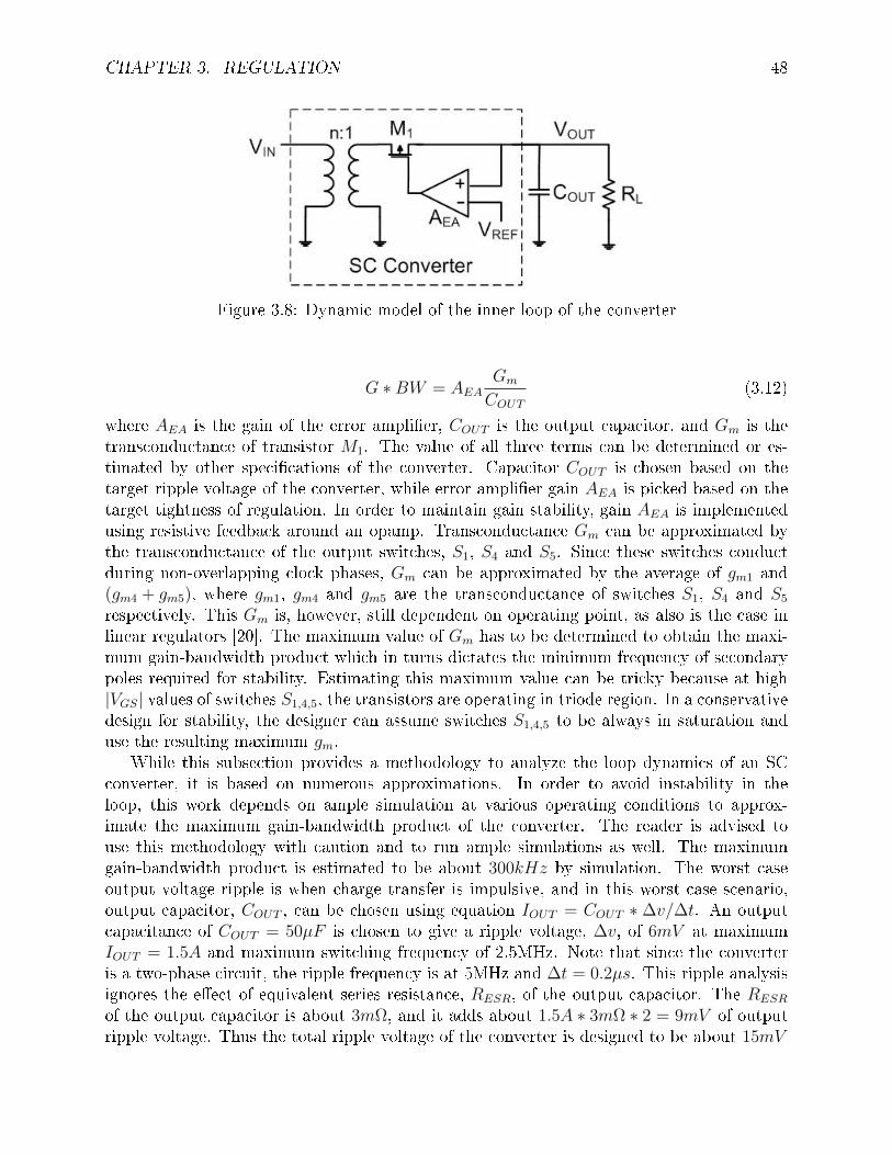
CHAPTER 3. REGULATION 48
Figure 3.8: Dynamic model of the inner loop of the converter
G ∗BW = AEAGm
COUT(3.12)
where AEA is the gain of the error amplier, COUT is the output capacitor, and Gm is thetransconductance of transistor M1. The value of all three terms can be determined or es-timated by other specications of the converter. Capacitor COUT is chosen based on thetarget ripple voltage of the converter, while error amplier gain AEA is picked based on thetarget tightness of regulation. In order to maintain gain stability, gain AEA is implementedusing resistive feedback around an opamp. Transconductance Gm can be approximated bythe transconductance of the output switches, S1, S4 and S5. Since these switches conductduring non-overlapping clock phases, Gm can be approximated by the average of gm1 and(gm4 + gm5), where gm1, gm4 and gm5 are the transconductance of switches S1, S4 and S5
respectively. This Gm is, however, still dependent on operating point, as also is the case inlinear regulators [20]. The maximum value of Gm has to be determined to obtain the maxi-mum gain-bandwidth product which in turns dictates the minimum frequency of secondarypoles required for stability. Estimating this maximum value can be tricky because at high|VGS| values of switches S1,4,5, the transistors are operating in triode region. In a conservativedesign for stability, the designer can assume switches S1,4,5 to be always in saturation anduse the resulting maximum gm.
While this subsection provides a methodology to analyze the loop dynamics of an SCconverter, it is based on numerous approximations. In order to avoid instability in theloop, this work depends on ample simulation at various operating conditions to approx-imate the maximum gain-bandwidth product of the converter. The reader is advised touse this methodology with caution and to run ample simulations as well. The maximumgain-bandwidth product is estimated to be about 300kHz by simulation. The worst caseoutput voltage ripple is when charge transfer is impulsive, and in this worst case scenario,output capacitor, COUT , can be chosen using equation IOUT = COUT ∗ ∆v/∆t. An outputcapacitance of COUT = 50µF is chosen to give a ripple voltage, ∆v, of 6mV at maximumIOUT = 1.5A and maximum switching frequency of 2.5MHz. Note that since the converteris a two-phase circuit, the ripple frequency is at 5MHz and ∆t = 0.2µs. This ripple analysisignores the eect of equivalent series resistance, RESR, of the output capacitor. The RESR
of the output capacitor is about 3mΩ, and it adds about 1.5A ∗ 3mΩ ∗ 2 = 9mV of outputripple voltage. Thus the total ripple voltage of the converter is designed to be about 15mV
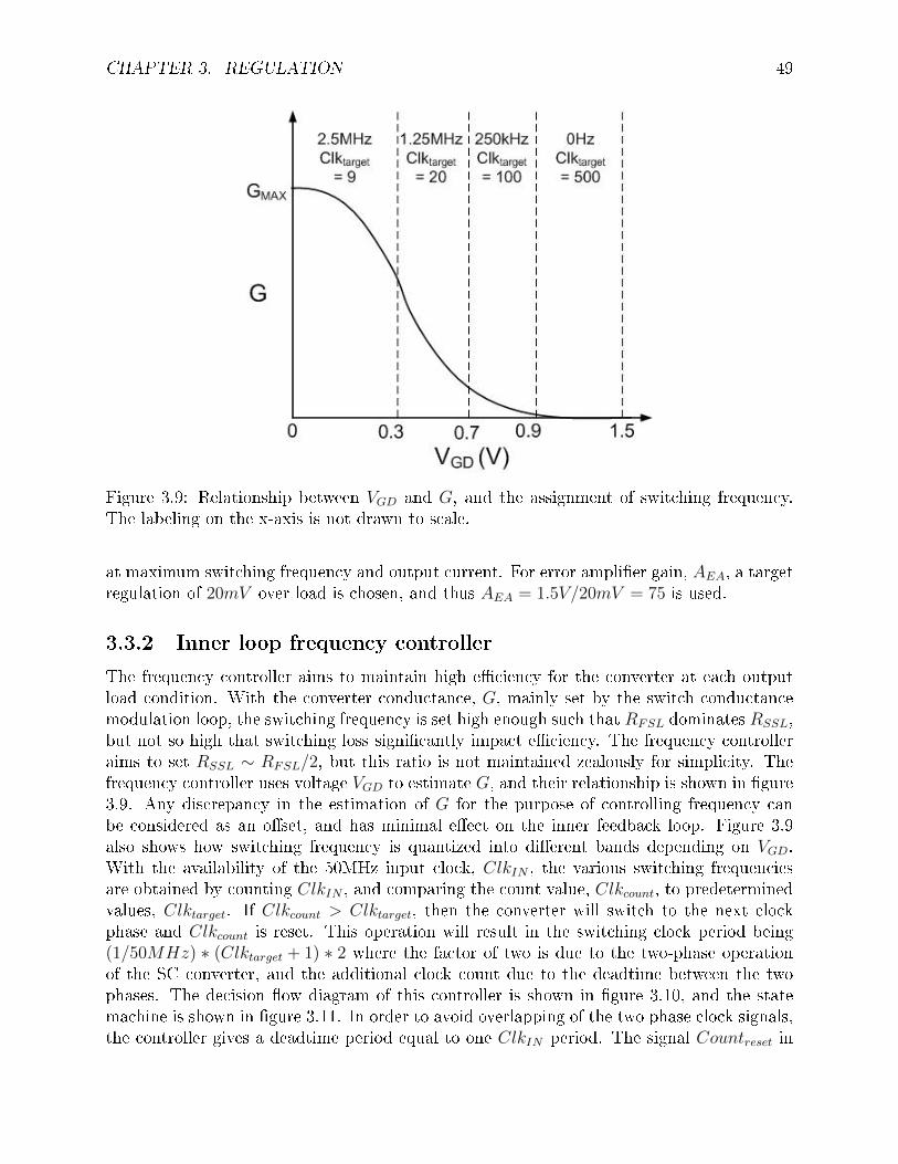
CHAPTER 3. REGULATION 49
Figure 3.9: Relationship between VGD and G, and the assignment of switching frequency.The labeling on the x-axis is not drawn to scale.
at maximum switching frequency and output current. For error amplier gain, AEA, a targetregulation of 20mV over load is chosen, and thus AEA = 1.5V/20mV = 75 is used.
3.3.2 Inner loop frequency controller
The frequency controller aims to maintain high eciency for the converter at each outputload condition. With the converter conductance, G, mainly set by the switch conductancemodulation loop, the switching frequency is set high enough such that RFSL dominates RSSL,but not so high that switching loss signicantly impact eciency. The frequency controlleraims to set RSSL ∼ RFSL/2, but this ratio is not maintained zealously for simplicity. Thefrequency controller uses voltage VGD to estimate G, and their relationship is shown in gure3.9. Any discrepancy in the estimation of G for the purpose of controlling frequency canbe considered as an oset, and has minimal eect on the inner feedback loop. Figure 3.9also shows how switching frequency is quantized into dierent bands depending on VGD.With the availability of the 50MHz input clock, ClkIN , the various switching frequenciesare obtained by counting ClkIN , and comparing the count value, Clkcount, to predeterminedvalues, Clktarget. If Clkcount > Clktarget, then the converter will switch to the next clockphase and Clkcount is reset. This operation will result in the switching clock period being(1/50MHz) ∗ (Clktarget + 1) ∗ 2 where the factor of two is due to the two-phase operationof the SC converter, and the additional clock count due to the deadtime between the twophases. The decision ow diagram of this controller is shown in gure 3.10, and the statemachine is shown in gure 3.11. In order to avoid overlapping of the two phase clock signals,the controller gives a deadtime period equal to one ClkIN period. The signal Countreset in
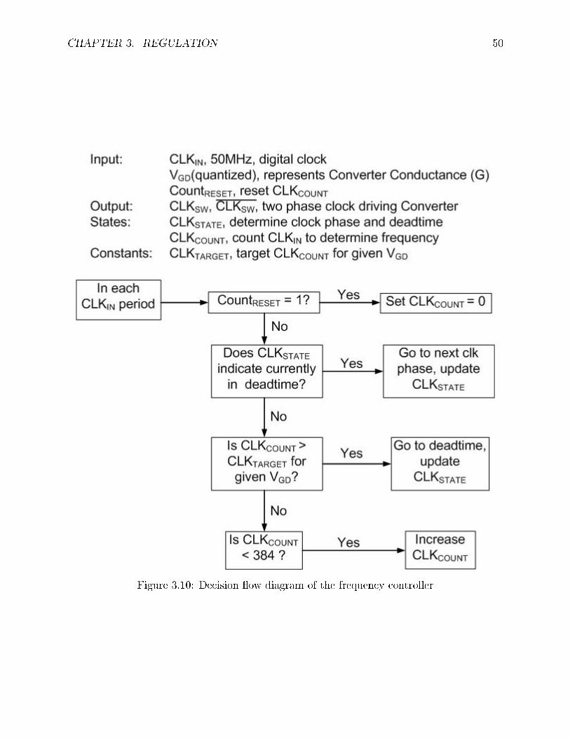
CHAPTER 3. REGULATION 50
Figure 3.10: Decision ow diagram of the frequency controller
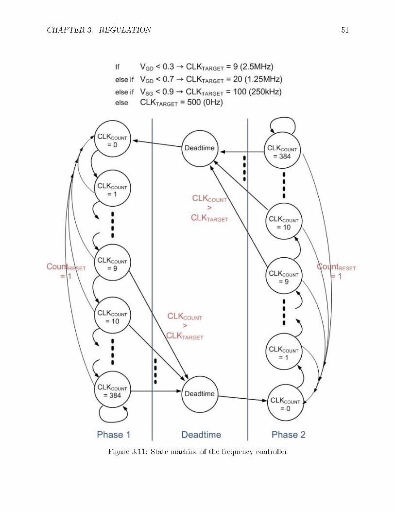
CHAPTER 3. REGULATION 51
Figure 3.11: State machine of the frequency controller
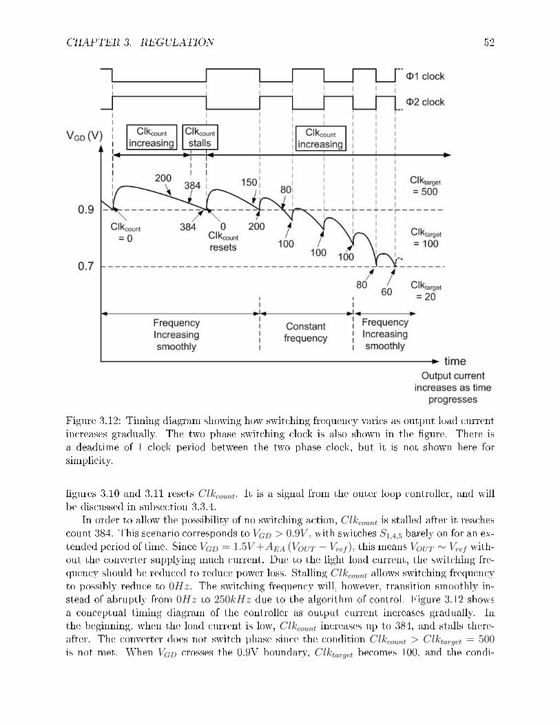
CHAPTER 3. REGULATION 52
Figure 3.12: Timing diagram showing how switching frequency varies as output load currentincreases gradually. The two phase switching clock is also shown in the gure. There isa deadtime of 1 clock period between the two phase clock, but it is not shown here forsimplicity.
gures 3.10 and 3.11 resets Clkcount. It is a signal from the outer loop controller, and willbe discussed in subsection 3.3.4.
In order to allow the possibility of no switching action, Clkcount is stalled after it reachescount 384. This scenario corresponds to VGD > 0.9V , with switches S1,4,5 barely on for an ex-tended period of time. Since VGD = 1.5V +AEA (VOUT − Vref ), this means VOUT ∼ Vref with-out the converter supplying much current. Due to the light load current, the switching fre-quency should be reduced to reduce power loss. Stalling Clkcount allows switching frequencyto possibly reduce to 0Hz. The switching frequency will, however, transition smoothly in-stead of abruptly from 0Hz to 250kHz due to the algorithm of control. Figure 3.12 showsa conceptual timing diagram of the controller as output current increases gradually. Inthe beginning, when the load current is low, Clkcount increases up to 384, and stalls there-after. The converter does not switch phase since the condition Clkcount > Clktarget = 500is not met. When VGD crosses the 0.9V boundary, Clktarget becomes 100, and the condi-
CHAPTER 3. REGULATION 53
tion Clkcount > Clktarget = 100 is met. The converter switches phase, and Clkcount resets.Note that the converter changes phase once it hits the VGD = 0.9V boundary, and is ef-fectively switching at a frequency between 0Hz and 250kHz. As output current furtherincreases, VGD decreases and the converter switches at a constant frequency of 250kHzwhile 0.7V < VGD < 0.9V . As VGD approaches the next boundary of 0.7V, the converteragain changes phase at the boundary. The timing diagram shows that the converter switchesat a constant frequency between boundaries, but frequency transitions smoothly from onefrequency to another at the boundary. This is eectively a multi-boundary version of thelower-bound hysteretic control proposed in [5].
3.3.3 Outer loop controller algorithm
The outer loop controller determines the optimal conversion ratio, n, of the controller in orderto maintain both regulation and eciency. The control algorithm is shown in gure 3.13, andis based on the G − VDROP space discussed in section 3.2. Maximum conductance, GMAX ,is detected by sensing whether VGD is less than 0.1V. As shown in gure 3.9, G approachesGMAX at low VGD, and thus VGD < 0.1V represents the scenario in which GMAX is reached.The curved portion of the upper eciency boundary in gure 3.6 is approximated by thestraight line G = GEB in gure 3.13. This simplies the complexity of detecting the eciencyboundary, although it introduces a region with more than one feasible conversion ratio andwhere eciency may not be optimized. Detecting whether G < GEB is not implementedusing VGD because while the lower bound of VGD is well controlled by the hysteretic nature ofthe frequency controller, the upper bound is prone to the ripple voltage transients. Instead,this controller makes use of freq < 100kHz to approximate G < GEB. The switchingfrequency of the converter is a monotonically increasing function of G controlled by thefrequency controller, and thus contains the information of G as well. Further, the switchingfrequency is conveniently represented by the digital signal Clkcount, with freq < 100kHzcorresponding to Clkcount > 250. Thus using frequency instead of VGD is a rather accurateand convenient way to approximate GEB.
When compared with gure 3.6, region E is an additional region in gure 3.13. Thisregion is dened by VGD > 1.4V , and represents the scenario in which the output voltagecontinues to rise even though the gate drive voltage for switches S1,4,5 is considerably lowerthan the threshold voltage. As VGD is used to represent G, this represents a non-intuitivesituation in which current continues to ow to the output even though G is already zero.This is not modeled in gure 3.8 or the G − VDROP space analysis in section 3.2. Thisscenario can happen when VIN increases signicantly or when a large unloading step occurs.Current may continue to ow to the drains of switches S1 and S4 in gure 3.7 via theirbody diodes. This allows current to ow to the output terminal even though the channelof PMOS transistors S1 and S4 are already turned o by the error amplier. In a step-down Dickson converter, switches S1 to S4 can be replaced by passive diodes, but they areimplemented with transistors in this work to reduce diode conduction loss. This scenariooccurs when these switches operate as diodes, as they naturally do. If this scenario happens,the conversion ratio of the converter should be increased, as indicated in gure 3.13.
Region F in gure 3.13 is also a new region when compared to gure 3.6. This regionrepresents a negative VDROP , which can happen in transient due to a reduction in VIN . The
CHAPTER 3. REGULATION 54
converter is out of regulation in this region, but the control algorithm discussed so far willreduce conversion ratio until the converter is back in region B and under regulation. This isbecause the inner controller will increaseG beyondGMAX , and cause the outer loop controllerto decrease conversion ratio. However, this response is based on feedback, and its speed islimited by stability considerations. One way to increase speed and break this requirementis to implement feedforward [27], which is the purpose of adding region F. When a negativeVDROP is detected, conversion ratio is reduced immediately and does not wait for the innerloop to increase G beyond GMAX . Depending on the value of VDROP , the conversion ratiois reduced by one or more steps and the response time is further reduced. The boundariesVFF1−VFF5 in gure 3.13 are only approximations since the exact number of steps requiredcannot be solely determined by VDROP but also need to take into account the load currentIOUT . For simplicity, IOUT is not measured, and this feedforward action is only designedto get the conversion ratio to roughly the correct value. The residual error is corrected byfeedback action.
One may notice that region F is the only region that causes multiple step changes in n ingure 3.13. This is not only because region F is the only feedforward region, but also becauseother regions either lack the information, or only require one step change as in the case ofregion D. Region A lacks the information to determine the optimal n since the required Gto maintain regulation with ncur is no longer available once G saturates at GMAX . RegionC also lacks the required information unless it is subdivided into smaller regions by moreeciency boundaries. Subdivision of region C is not implemented in this work for simplicity,and also because the converter is under regulation in region C and a fast response is notneeded. Region E probably requires at least two steps increase in n, but the exact numberis dicult to determine since this is an unmodeled exceptional case. Thus for uniformity, allchanges in n occur in one step, with the only exception of feedforward represented by regionF.
Region G is the last additional region in gure 3.13. It is added to protect the converterfrom over-current conditions, and is detected by G > GMAX and VDROP > VOCP . VoltageVOCP is given by:
VOCP =IMAX
GMAX
(3.13)
where IMAX is the maximum current rating of the converter. If IMAX is reached, the powerconsumed by the converter may exceed its safety limit, and the converter should shut down.This is implemented by not reducing n, and allowing VOUT to drop. As VOUT reduces,the controller blocks will shut down automatically as VOUT serve as their supply rail. Theconverter will stop switching and shut down. Thus this prevents the converter from supplyingmore current than designed, and protects it and the load from an over-current condition.
3.3.4 Outer loop controller state machine
Figure 3.14 shows the decision ow diagram of the outer loop controller, and gure 3.15shows the state machine. The state machine has a number of states as shown in gure 3.14.State PeriodCount is used to count the number of clock phase periods that the converter hasexperienced after a change in conversion ratio. This number is reset after a conversion ratio
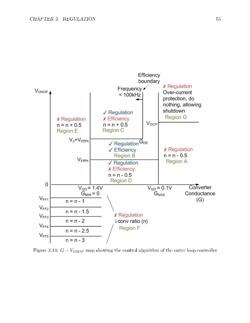
CHAPTER 3. REGULATION 55
Figure 3.13: G− VDROP map showing the control algorithm of the outer loop controller
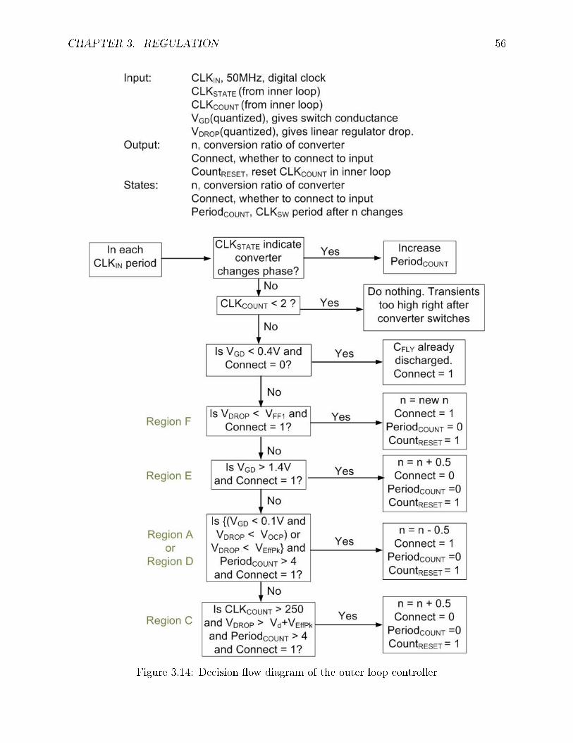
CHAPTER 3. REGULATION 56
Figure 3.14: Decision ow diagram of the outer loop controller
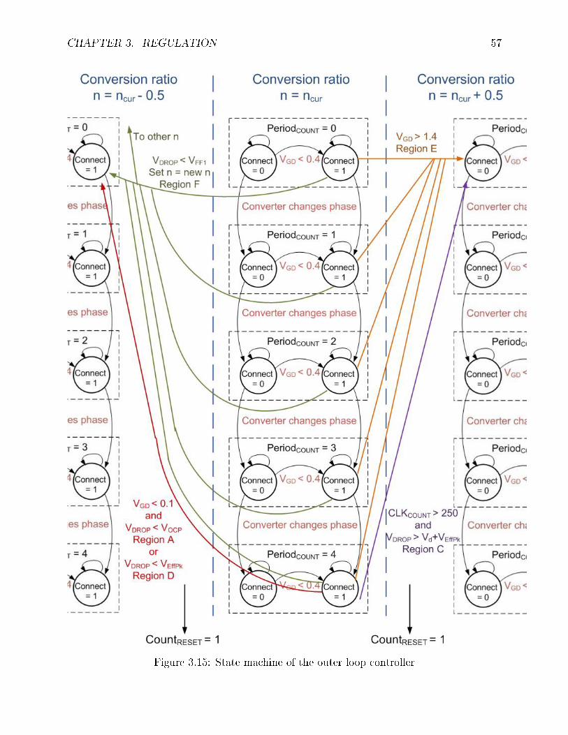
CHAPTER 3. REGULATION 57
Figure 3.15: State machine of the outer loop controller
CHAPTER 3. REGULATION 58
change, and is incremented by 1 each time the converter changes phase until PeriodCount = 4is reached. State PeriodCount = 4 means the converter has changed phase four times, andthus 2 switching periods have elapsed. This information is used to determine whether theconverter is still under a transient condition after a conversion ratio change, meaning thevalue of G does not yet represent a converged value. Waiting for the regulation to settle downbefore changing n again allows a more accurate decision, but it slows down the response ifmore than 1 step change in n is needed due to large variations in IOUT . This design choosesan interval of 2 switching period as a compromise between these two requirements. If theconverter enters into region A, C or D, the controller only changes n if PeriodCount = 4.However, if the converter enters into region E or F, n is immediately changed regardless ofPeriodCount because dynamics only causes uncertainty in G and these two regions do notdepend on G. Region F is solely determined by VDROP , and entry into region E can only becaused by a VIN that is too high. The measurement results can however be aected by theringing of the supply rails after a switch turns on and o, as discussed in subsection 4.11.This eect is avoided by introducing a blanking period implemented by no action if ClkCountfrom the inner loop is less than 2.
As indicated in gures 3.14 and 3.15, there is a state called Connect, which indicateswhether the converter is connected to the input source. The converter is disconnected fromthe input source after n is increased, and this is done by not turning on any of switchesSCV 1 − SCV 6 in gure 2.7. The reason for this is because the residual charge in the yingcapacitor can cause VOUT to overshoot when conversion ratio is changed with an increase inn. For example, when the conversion ratio is increased, the ying capacitors can push VOUTto below its steady state value in a transient. The inner loop controller will respond to thisdip in VOUT by increasing G, and may even push G beyond GMAX in the transient. Onesolution to prevent this transient from happening is to disconnect from the input terminalafter an increase in conversion ratio, and wait until the voltages in the ying capacitorsare drawn down before connecting back to the input. This operation corresponds to usingthe stored energy in the ying capacitors to supply the output load temporarily. If theconverter is not disconnected from the input, some of the stored energy is actually beingpushed back to the source during this transient. With the input disconnected, as the storedenergy is being used, G will increase, and the converter is connected back to the input whenVGD < 0.4V . It is only after the converter is connected to the input that the controller willconsider changing n again. During an unloading step that requires multiple step increasesin n, this sequence can take a long time. However, since the converter is under regulation inthis period of time, this is not a concern.
As discussed so far, the outer loop controller uses many signals from the inner loop,but the communication is actually two way, and the outer loop also aects the inner loop.Whenever the outer loop changes n, it instructs the inner loop to reset ClkCount, and this isdone by setting the signal CountReset = 1. Resetting ClkCount after a conversion ratio changeensures that there is enough time for charge to ow among the power-train capacitors. Afterthe converter changes phase or conversion ratio, charges start to ow among capacitorswith time constant equal to that of an L-R-C network, where L comes from the parasiticinductance of the bondwires. Resetting ClkCount ensures that the charges have at least9 ClkIN periods to ow, and so charge ow is not interrupted when the current peaks.Interrupting charge ow can cause signicant ringings in the power rails, as discussed in
CHAPTER 3. REGULATION 59
subsection 4.11.
3.3.5 Controller simulation results
Figure 3.16 shows a simulation of the converter for a moderate change in load current levels.The input voltage is at 12.5V, and the conversion ratio is maintained at 8:1 throughoutthe simulation because maximum converter conductance, GMAX , has not been reached yet.This simulation is intended to show the behavior of the inner loop controller. As shown inthe simulation, the output voltage level droops as output current increases. This changein output voltage is necessary to increase the input voltage to the error amplier, which inturn increases G and keeps the converter under regulation. This is the familiar load-linebehavior occurring in a buck converter controller and in a linear regulator. The simulationalso shows that the switching frequency of the converter increases as output voltage droops.The simulation closely resembles the timing diagram of the frequency controller shown ingure 3.12. The region where the switching frequency remains constant, and where it istransitioning smoothly from one frequency to another at a boundary are also labeled in thesimulation.
Figure 3.17 shows a simulation result for a large change in output current level. In orderto accommodate this large output current, the converter changes conversion ratio, n, twice,as shown in the gure on the left hand side. After n changes, the output voltage increasesbecause with a larger VDROP , required G reduces, and thus the input voltage of the erroramplier also reduces. This reduction in G accompanies a reduction in switching frequency,and thus the ripple voltage increases after n changes. The signicantly larger ripple for oneclock cycle after the second n change is due to the residual charge in the ying capacitors.The simulation on the right hand side shows the behavior of the controller for a large currentstep. Although the current ramp simulation shows that n only needs to reduce twice for thisIOUT change, n reduces 3 times in the current step simulation. This is due to the controllerresponding to the large initial transient in VOUT . The converter stays at the conversion ration− 3 after the transient and does not change to n− 2 due to the build in hysteresis region.One way to avoid this over-reaction is to wait for a longer period of time after n changesbefore allowing it to change again. However, in the cases where n indeed needs to changemore than once, this can result in a signicant transient in VOUT . Thus this wait timeneeds to be chosen based on a compromise. Through ample simulations, a wait time offour clock period, around 80ns, is chosen, and thus the outer loop controller is not allowedto change conversion ratio when PeriodCount < 4, as discussed in subsection 3.3.4.
As discussed in subsection 3.3.4, the converter disconnects from the input source after nincreases, and uses the stored charge in the ying capacitors. Figure 3.18 shows a simulationof this behavior. The simulation begins with a step increase in IOUT to get the controllerto decrease conversion ratio. The change in conversion ratio is shown by the change in theleast signicant bit (LSB) of the conversion ratio. This is followed by an unloading step.As shown in the simulation, the converter is disconnected from the input source once nincreases, as shown by the signal NoConnect. As the stored energy in the ying capacitorsis being consumed, the converter switches faster. The converter nally connects back to theinput source at around 180µs.
Figure 3.19 shows a simulation of the behavior of the converter for changes in input

CHAPTER 3. REGULATION 60
Figure
3.16:Simulation
displaysoutputvoltageof
thecontrollerforamoderatechange
inoutputcurrentlevel.Thelefthand
sideplotshow
stheresponse
witharampchange
inoutputcurrentwhereastherighthandsideplotshow
stheresponse
witha
step
change
inoutputcurrent.
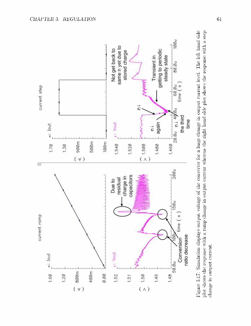
CHAPTER 3. REGULATION 61
Figure
3.17:Simulation
displaysoutputvoltageof
theconverter
foralargechange
inoutputcurrentlevel.Thelefthandside
plotshow
stheresponse
witharampchange
inoutputcurrentwhereastherighthandsideplotshow
stheresponse
withastep
change
inoutputcurrent.
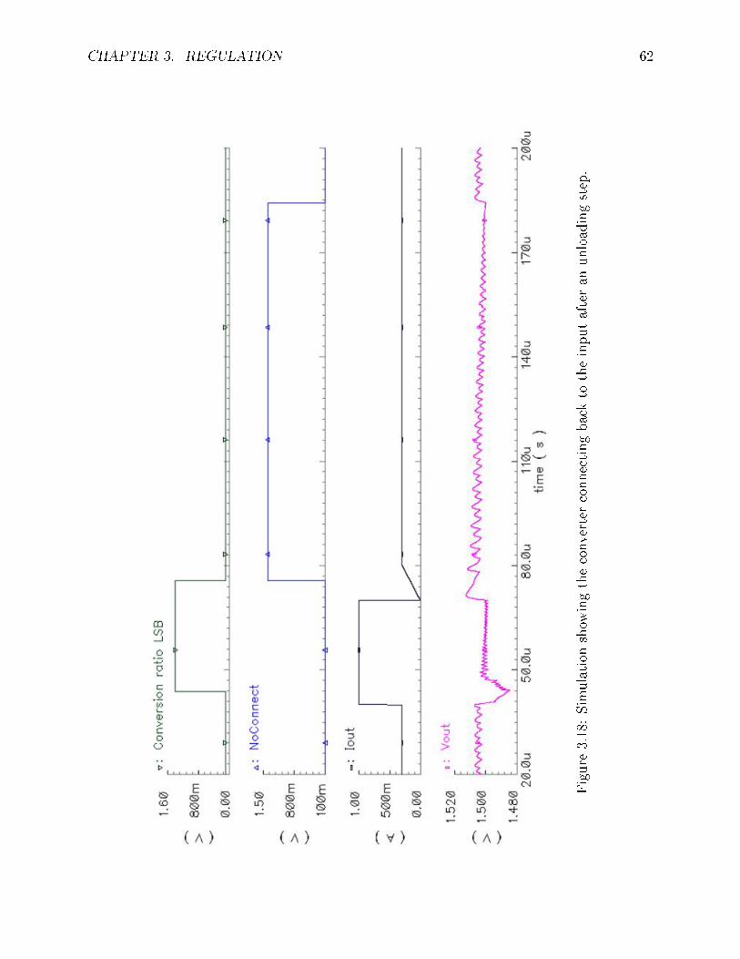
CHAPTER 3. REGULATION 62
Figure
3.18:Simulation
show
ingtheconverter
connectingbackto
theinputafteran
unloadingstep.
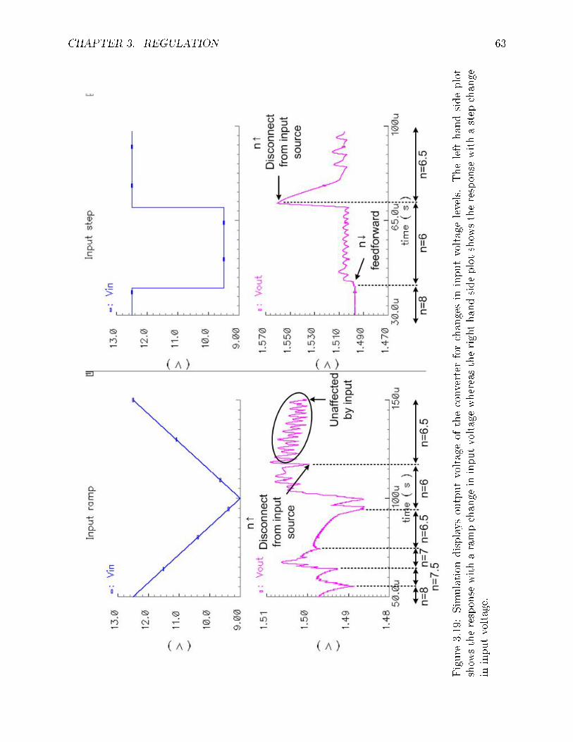
CHAPTER 3. REGULATION 63
Figure
3.19:Simulation
displaysoutputvoltageof
theconverter
forchangesin
inputvoltagelevels.Thelefthandsideplot
show
stheresponse
witharampchange
ininputvoltagewhereastherighthandsideplotshow
stheresponse
withastep
change
ininputvoltage.
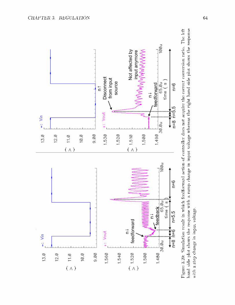
CHAPTER 3. REGULATION 64
Figure
3.20:Simulation
resultin
whichfeedforwardaction
ofcontrollerdoes
not
acquirethecorrectconversionratio.
Theleft
handsideplotshow
stheresponse
witharampchange
ininputvoltagewhereastherighthandsideplotshow
stheresponse
withastep
change
ininputvoltage.
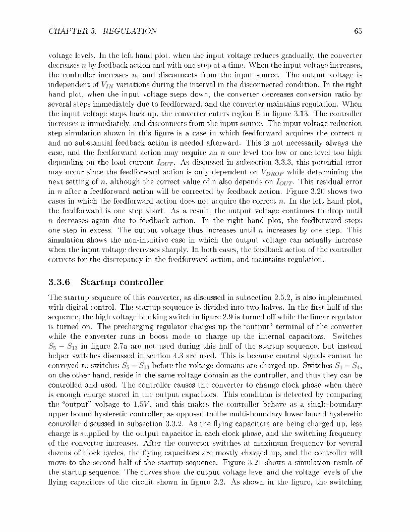
CHAPTER 3. REGULATION 65
voltage levels. In the left hand plot, when the input voltage reduces gradually, the converterdecreases n by feedback action and with one step at a time. When the input voltage increases,the controller increases n, and disconnects from the input source. The output voltage isindependent of VIN variations during the interval in the disconnected condition. In the righthand plot, when the input voltage steps down, the converter decreases conversion ratio byseveral steps immediately due to feedforward, and the converter maintains regulation. Whenthe input voltage steps back up, the converter enters region E in gure 3.13. The controllerincreases n immediately, and disconnects from the input source. The input voltage reductionstep simulation shown in this gure is a case in which feedforward acquires the correct nand no substantial feedback action is needed afterward. This is not necessarily always thecase, and the feedforward action may acquire an n one level too low or one level too highdepending on the load current IOUT . As discussed in subsection 3.3.3, this potential errormay occur since the feedforward action is only dependent on VDROP while determining thenext setting of n, although the correct value of n also depends on IOUT . This residual errorin n after a feedforward action will be corrected by feedback action. Figure 3.20 shows twocases in which the feedforward action does not acquire the correct n. In the left hand plot,the feedforward is one step short. As a result, the output voltage continues to drop untiln decreases again due to feedback action. In the right hand plot, the feedforward stepsone step in excess. The output voltage thus increases until n increases by one step. Thissimulation shows the non-intuitive case in which the output voltage can actually increasewhen the input voltage decreases sharply. In both cases, the feedback action of the controllercorrects for the discrepancy in the feedforward action, and maintains regulation.
3.3.6 Startup controller
The startup sequence of this converter, as discussed in subsection 2.5.2, is also implementedwith digital control. The startup sequence is divided into two halves. In the rst half of thesequence, the high voltage blocking switch in gure 2.9 is turned o while the linear regulatoris turned on. The precharging regulator charges up the output terminal of the converterwhile the converter runs in boost mode to charge up the internal capacitors. SwitchesS5 − S13 in gure 2.7a are not used during this half of the startup sequence, but insteadhelper switches discussed in section 4.3 are used. This is because control signals cannot beconveyed to switches S5− S13 before the voltage domains are charged up. Switches S1− S4,on the other hand, reside in the same voltage domain as the controller, and thus they can becontrolled and used. The controller causes the converter to change clock phase when thereis enough charge stored in the output capacitors. This condition is detected by comparingthe output voltage to 1.5V , and this makes the controller behave as a single-boundaryupper bound hysteretic controller, as opposed to the multi-boundary lower bound hystereticcontroller discussed in subsection 3.3.2. As the ying capacitors are being charged up, lesscharge is supplied by the output capacitor in each clock phase, and the switching frequencyof the converter increases. After the converter switches at maximum frequency for severaldozens of clock cycles, the ying capacitors are mostly charged up, and the controller willmove to the second half of the startup sequence. Figure 3.21 shows a simulation result ofthe startup sequence. The curves show the output voltage level and the voltage levels of theying capacitors of the circuit shown in gure 2.2. As shown in the gure, the switching
CHAPTER 3. REGULATION 66
Figure3.21:Simulation
ofthestartupsequence
show
ingtheoutputvoltageandthevoltagelevelsofthevariousyingcapacitors
ofthecircuitshow
nin
gure
2.2.
CHAPTER 3. REGULATION 67
frequency of the converter increases during the rst half of the startup sequence, and remainsconstant for a certain period of time before entering the second half of the startup sequence.
In the second half of the startup sequence, all the main switches S5 − S13 are utilized inorder to fully charge up the ying capacitors. This is necessary because the helper switchesare small in size, and thus cause voltage drop in the voltage levels of the ying capacitors.This can be explained with the fast switching limit of the output referred resistance of anSC converter, as discussed in section 1.1. As shown in gure 3.21, the voltage levels of theying capacitors increase signicantly as the converter enters the second half of the startupsequence. Further, as discussed in section 4.3, the helper switches cause a diode drop in thelast voltage level, and cannot fully charge up the last ying capacitor. This is evidenced inthe simulation by the smaller voltage dierence between the top two curves when comparedto the other curves in the rst half of the startup sequence. With the voltage domains mostlycharged up, the levelshifter circuits can now function, and the main switches can be usedto eliminate the residual error in the ying capacitor voltage levels. In the simulation, thevoltage dierence among the curves becomes equal in the second half of the startup sequence.However, as discussed in section 4.1, the speed of the levelshifter circuit is greatly reducedwhen the voltage level of the top voltage domain is reduced. Thus the converter is designedto switch at 1/10 of the maximum frequency in this second half of the startup sequence.This reduced frequency is also visible in the simulation.
During the second half of the startup sequence, the high voltage blocking switch in gure2.9 is turned on since it is no longer needed for protection. However, switches SCV 1 − SCV 6
in gure 2.7a remains o so the converter is still eectively disconnected from the inputsource. The controller will make use of the information on VDROP during this period oftime to determine a rough estimate for optimal conversion ratio, n. After the converterruns for 64 cycles, or about 256ms, the startup sequence is done, and the converter willstart running in normal mode with this newly determined n. The normal mode algorithmdiscussed in subsections 3.3.3 and 3.3.4 will correct for any remaining error in n. Theprecharging regulator is turned o after the startup sequence is completed.
CHAPTER 4. CIRCUITS 68
Chapter 4
Circuits
Chapters 1 to 3 discuss the overall picture of this design, and this chapter focuses on thecircuit details used to implement the design. The controller in this design powers fromthe output of the converter, as do most circuits discussed in this chapter, unless otherwisespecied. For simplicity, the circuits are labeled as directly powering from the output, butin actual implementation, they power from a ltered supply connected to the output. Thisltered supply uses on-chip capacitors to eliminate the transients on the output rail dueto parasitic inductance and the switching action of the converter. There are two lteredsupplies, one for the analog circuits and one for the digital circuits. The two supplies areseparated so that the analog circuits, which are less power-hungry but more prone to noise,are not aected by switching noise of the digital circuits.
4.1 Levelshifters
As discussed in section 2.2, the converter is divided into various voltage domains, and thuslevelshifters are needed to convey signals among them. Figure 4.1 shows the levelshifterdesign implemented in this work, which is similar to that in reference [28]. To obtain morevoltage domains, as used in the converter shown in gure 2.2, voltage domain 2 is instantiatedmultiple times depending on the number of voltage domains required, but is only shown oncein the gure for simplicity. The circuit consists of two strings of transistors connected atthe top by a cross-coupled half-latch. It operates with either NMOS transistors M1 or M2
pulling down one string, and then the cross-coupled PMOS pair M11 and M12 pulling up theother string. Transistors M3−M10 act as cascode devices to limit the voltage swing at eachnode, such that each transistor is only subjected to a fraction of the overall voltage levelapplied to these two strings of transistors. Capacitors C1 − C6 are added such that all theoutput signals (VOUT1 − VOUT3) are initially low, and cause the main switches S5 − S13 ingure 2.7a to stay o during the rst half of the startup sequence.
In order for the levelshifter to switch state, transistor M11 or M12 has to be overpowered,and thus the sizing of transistors in gure 4.1 have to be carefully chosen. Transistors M1
and M2 have to be sized stronger than transistors M11 and M12 in all cases. If the voltagelevel M11 or M12 of any voltage domain deviates signicantly from design value, the relativestrength of the transistors may change and the levelshifter will fail to switch state. This
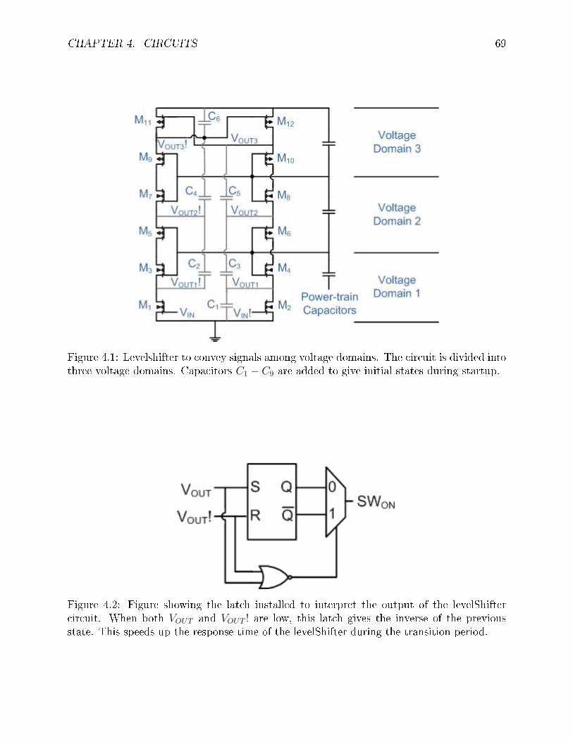
CHAPTER 4. CIRCUITS 69
Figure 4.1: Levelshifter to convey signals among voltage domains. The circuit is divided intothree voltage domains. Capacitors C1 − C9 are added to give initial states during startup.
Figure 4.2: Figure showing the latch installed to interpret the output of the levelShiftercircuit. When both VOUT and VOUT ! are low, this latch gives the inverse of the previousstate. This speeds up the response time of the levelShifter during the transition period.
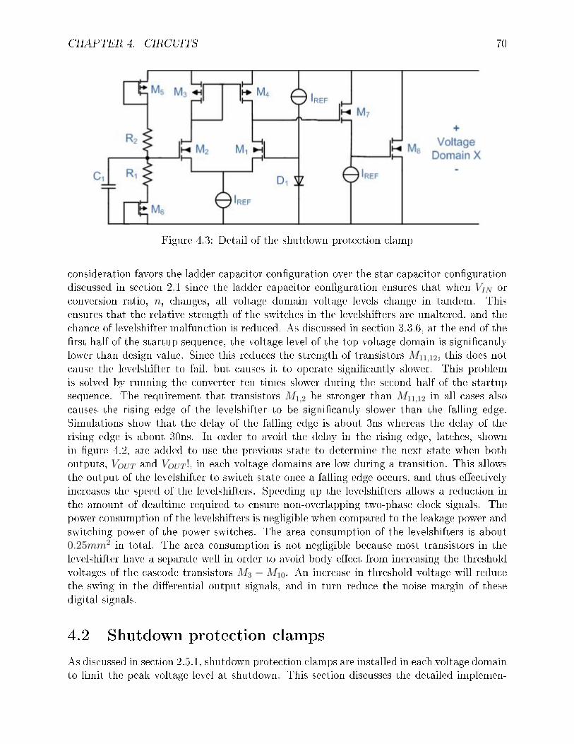
CHAPTER 4. CIRCUITS 70
Figure 4.3: Detail of the shutdown protection clamp
consideration favors the ladder capacitor conguration over the star capacitor congurationdiscussed in section 2.1 since the ladder capacitor conguration ensures that when VIN orconversion ratio, n, changes, all voltage domain voltage levels change in tandem. Thisensures that the relative strength of the switches in the levelshifters are unaltered, and thechance of levelshifter malfunction is reduced. As discussed in section 3.3.6, at the end of therst half of the startup sequence, the voltage level of the top voltage domain is signicantlylower than design value. Since this reduces the strength of transistors M11,12, this does notcause the levelshifter to fail, but causes it to operate signicantly slower. This problemis solved by running the converter ten times slower during the second half of the startupsequence. The requirement that transistors M1,2 be stronger than M11,12 in all cases alsocauses the rising edge of the levelshifter to be signicantly slower than the falling edge.Simulations show that the delay of the falling edge is about 3ns whereas the delay of therising edge is about 30ns. In order to avoid the delay in the rising edge, latches, shownin gure 4.2, are added to use the previous state to determine the next state when bothoutputs, VOUT and VOUT !, in each voltage domains are low during a transition. This allowsthe output of the levelshifter to switch state once a falling edge occurs, and thus eectivelyincreases the speed of the levelshifters. Speeding up the levelshifters allows a reduction inthe amount of deadtime required to ensure non-overlapping two-phase clock signals. Thepower consumption of the levelshifters is negligible when compared to the leakage power andswitching power of the power switches. The area consumption of the levelshifters is about0.25mm2 in total. The area consumption is not negligible because most transistors in thelevelshifter have a separate well in order to avoid body eect from increasing the thresholdvoltages of the cascode transistors M3 −M10. An increase in threshold voltage will reducethe swing in the dierential output signals, and in turn reduce the noise margin of thesedigital signals.
4.2 Shutdown protection clamps
As discussed in section 2.5.1, shutdown protection clamps are installed in each voltage domainto limit the peak voltage level at shutdown. This section discusses the detailed implemen-
CHAPTER 4. CIRCUITS 71
tation of these shutdown protection clamps. A conceptual design of the clamp circuit wasshown in gure 2.8, while its detailed schematic is shown in gure 4.3. The clamp consistsof an NMOS dierential pair that compares the divided voltage level of the voltage domainto a reference voltage, and turns on transistor M8 if over-voltage is detected. This circuitis designed to draw minimal power such that the standby current of these clamps does notexceed the leakage current of the power-train switches. Since the clamp protects the con-verter from voltage drift in the power-train capacitor network during shutdown, it can berather slow. Further, since 2V transistors and 5V transistors are used in 1.5V and 3V voltagedomains respectively, the clamp turn on voltage is designed to be well above the workingvoltage domain levels, and thus high accuracy is not required in these clamps. With thisspecication, several features of these clamps are designed to strategically tradeo accuracyand speed with power consumption.
The reference voltage is generated by passing a reference current, Iref , through a pndiode, where all Iref in gure 4.3 are generated by the current reference circuit discussed insection 4.9. The reference voltage from the bandgap reference discussed in section 4.10 is notused because it is more power hungry than the current reference, and is only implementedin voltage domain 1 in gure 2.2. On the other hand, protection clamps are required in allvoltage domains, and thus the low power current reference is implemented in each voltagedomain to provide the reference current for each clamp. Transistors M5 and M6 are addedto reduce the voltage drop across the resistive divider, such that the current ow can beminimized. Due to the high resistance (∼ 1MΩ each) of resistors R1 and R2, the gate ofM1 is prone to capacitive coupling into the node. Since the clamp circuit resides in voltagedomains that move relative to the the substrate ground in each clock phase, coupling canoccur through parasitic capacitance to the substrate. Capacitor C1 is added to reduce thiscoupling eect and to prevent the clamp from inadvertently turning on. A source followerconsisting of transistor M7 is added so that the dierential pair can be of minimum size andconsume minimal power. This source follower also levelshifts the output of the dierentialpair such that the VGS of transistor M8 is at 0V when it is turned o. Each clamp circuitis designed to draw about 200nA when o, and draw about 5mA when on. The area of theclamp circuits is mostly made up of the high resistance resistors R1 and R2, and is about0.1mm2 in total. The total combined static power drawn by all the clamp circuits togetheris about 6µW .
4.3 Startup helper circuits
As discussed in subsection 3.3.6, the main switches S5−S13 in gure 2.7a are not utilized inthe rst half of the startup sequence but helper switches are used instead. Figure 4.4 showsthe startup helper circuits implemented in this work, motivated by the scheme used in [18].It consists of an inverter driving an NMOS transistor parallel to the main switch in eachvoltage domain. In the beginning of the startup sequence, switches S1 − S4 are driven in atwo phase manner as indicated in the gure. Switches S5 − S13 all have gates connected tosources, but since the converter is running in boost mode during startup, the voltages arereversed and they act like diodes. Charges are thus being pushed up this ladder of capacitorssequentially as the converter changes clock phase. However, pushing charges through diodes
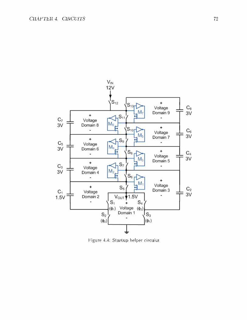
CHAPTER 4. CIRCUITS 72
Figure 4.4: Startup helper circuits
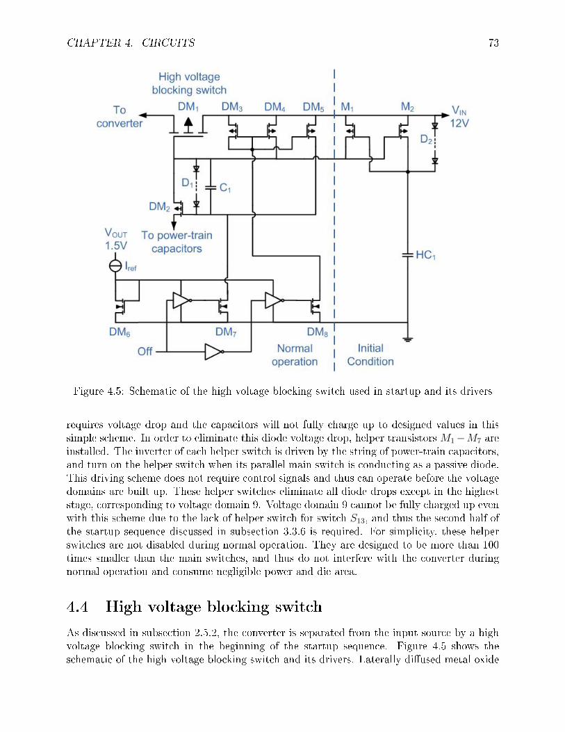
CHAPTER 4. CIRCUITS 73
Figure 4.5: Schematic of the high voltage blocking switch used in startup and its drivers
requires voltage drop and the capacitors will not fully charge up to designed values in thissimple scheme. In order to eliminate this diode voltage drop, helper transistors M1−M7 areinstalled. The inverter of each helper switch is driven by the string of power-train capacitors,and turn on the helper switch when its parallel main switch is conducting as a passive diode.This driving scheme does not require control signals and thus can operate before the voltagedomains are built up. These helper switches eliminate all diode drops except in the higheststage, corresponding to voltage domain 9. Voltage domain 9 cannot be fully charged up evenwith this scheme due to the lack of helper switch for switch S13, and thus the second half ofthe startup sequence discussed in subsection 3.3.6 is required. For simplicity, these helperswitches are not disabled during normal operation. They are designed to be more than 100times smaller than the main switches, and thus do not interfere with the converter duringnormal operation and consume negligible power and die area.
4.4 High voltage blocking switch
As discussed in subsection 2.5.2, the converter is separated from the input source by a highvoltage blocking switch in the beginning of the startup sequence. Figure 4.5 shows theschematic of the high voltage blocking switch and its drivers. Laterally diused metal oxide
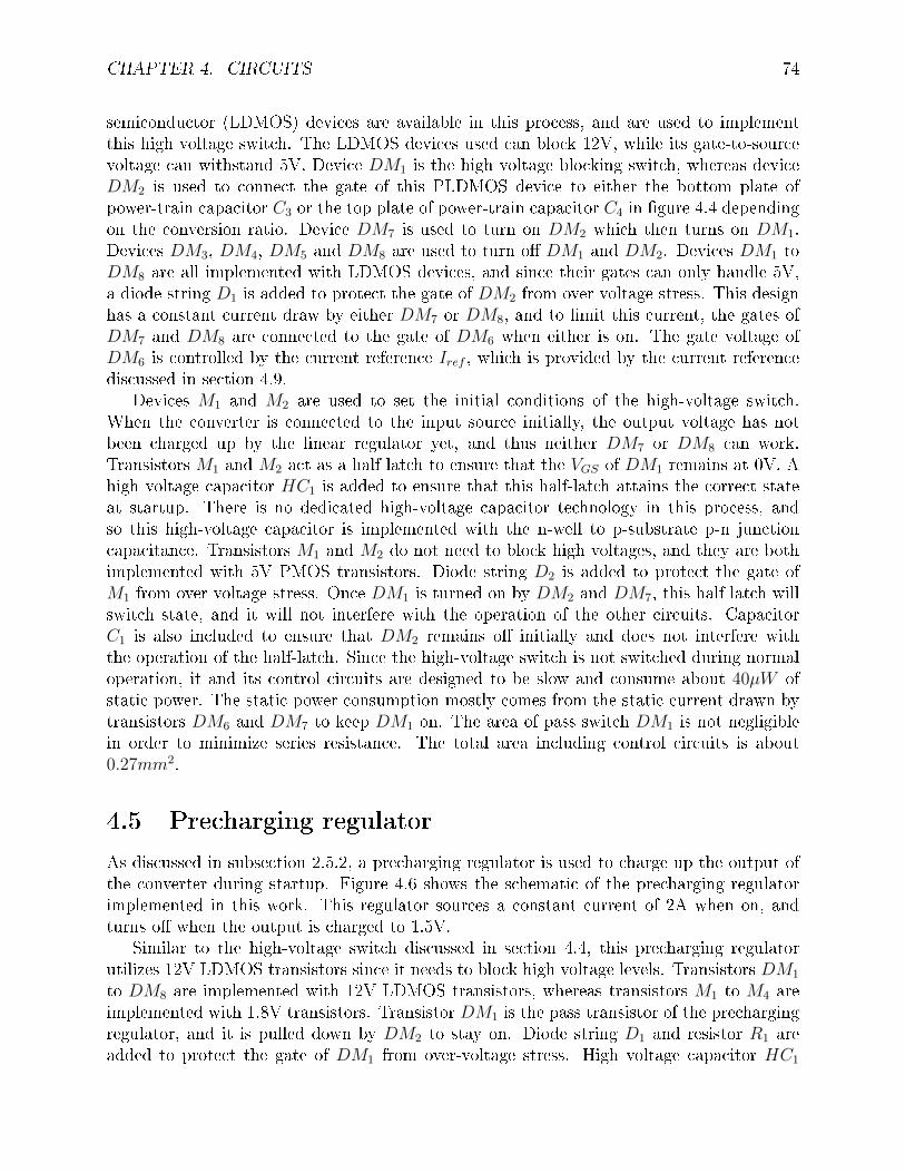
CHAPTER 4. CIRCUITS 74
semiconductor (LDMOS) devices are available in this process, and are used to implementthis high voltage switch. The LDMOS devices used can block 12V, while its gate-to-sourcevoltage can withstand 5V. Device DM1 is the high voltage blocking switch, whereas deviceDM2 is used to connect the gate of this PLDMOS device to either the bottom plate ofpower-train capacitor C3 or the top plate of power-train capacitor C4 in gure 4.4 dependingon the conversion ratio. Device DM7 is used to turn on DM2 which then turns on DM1.Devices DM3, DM4, DM5 and DM8 are used to turn o DM1 and DM2. Devices DM1 toDM8 are all implemented with LDMOS devices, and since their gates can only handle 5V,a diode string D1 is added to protect the gate of DM2 from over voltage stress. This designhas a constant current draw by either DM7 or DM8, and to limit this current, the gates ofDM7 and DM8 are connected to the gate of DM6 when either is on. The gate voltage ofDM6 is controlled by the current reference Iref , which is provided by the current referencediscussed in section 4.9.
Devices M1 and M2 are used to set the initial conditions of the high-voltage switch.When the converter is connected to the input source initially, the output voltage has notbeen charged up by the linear regulator yet, and thus neither DM7 or DM8 can work.Transistors M1 and M2 act as a half latch to ensure that the VGS of DM1 remains at 0V. Ahigh voltage capacitor HC1 is added to ensure that this half-latch attains the correct stateat startup. There is no dedicated high-voltage capacitor technology in this process, andso this high-voltage capacitor is implemented with the n-well to p-substrate p-n junctioncapacitance. Transistors M1 and M2 do not need to block high voltages, and they are bothimplemented with 5V PMOS transistors. Diode string D2 is added to protect the gate ofM1 from over voltage stress. Once DM1 is turned on by DM2 and DM7, this half latch willswitch state, and it will not interfere with the operation of the other circuits. CapacitorC1 is also included to ensure that DM2 remains o initially and does not interfere withthe operation of the half-latch. Since the high-voltage switch is not switched during normaloperation, it and its control circuits are designed to be slow and consume about 40µW ofstatic power. The static power consumption mostly comes from the static current drawn bytransistors DM6 and DM7 to keep DM1 on. The area of pass switch DM1 is not negligiblein order to minimize series resistance. The total area including control circuits is about0.27mm2.
4.5 Precharging regulator
As discussed in subsection 2.5.2, a precharging regulator is used to charge up the output ofthe converter during startup. Figure 4.6 shows the schematic of the precharging regulatorimplemented in this work. This regulator sources a constant current of 2A when on, andturns o when the output is charged to 1.5V.
Similar to the high-voltage switch discussed in section 4.4, this precharging regulatorutilizes 12V LDMOS transistors since it needs to block high voltage levels. Transistors DM1
to DM8 are implemented with 12V LDMOS transistors, whereas transistors M1 to M4 areimplemented with 1.8V transistors. Transistor DM1 is the pass transistor of the prechargingregulator, and it is pulled down by DM2 to stay on. Diode string D1 and resistor R1 areadded to protect the gate of DM1 from over-voltage stress. High voltage capacitor HC1
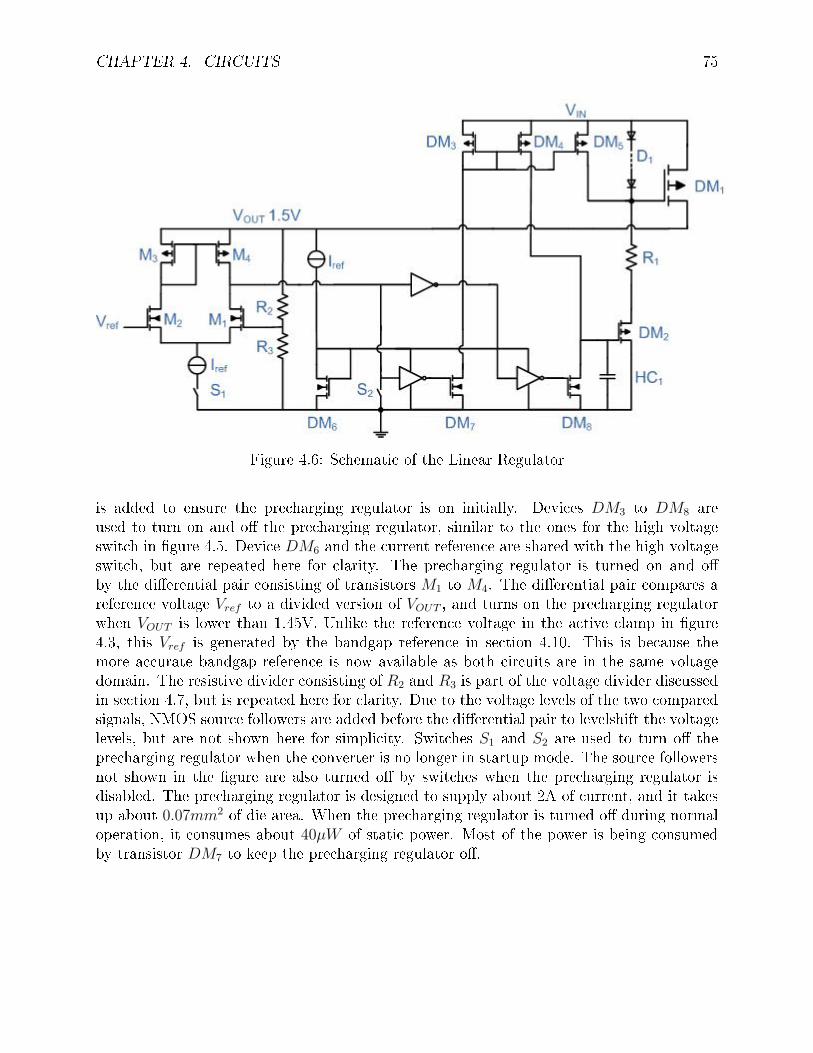
CHAPTER 4. CIRCUITS 75
Figure 4.6: Schematic of the Linear Regulator
is added to ensure the precharging regulator is on initially. Devices DM3 to DM8 areused to turn on and o the precharging regulator, similar to the ones for the high voltageswitch in gure 4.5. Device DM6 and the current reference are shared with the high voltageswitch, but are repeated here for clarity. The precharging regulator is turned on and oby the dierential pair consisting of transistors M1 to M4. The dierential pair compares areference voltage Vref to a divided version of VOUT , and turns on the precharging regulatorwhen VOUT is lower than 1.45V. Unlike the reference voltage in the active clamp in gure4.3, this Vref is generated by the bandgap reference in section 4.10. This is because themore accurate bandgap reference is now available as both circuits are in the same voltagedomain. The resistive divider consisting of R2 and R3 is part of the voltage divider discussedin section 4.7, but is repeated here for clarity. Due to the voltage levels of the two comparedsignals, NMOS source followers are added before the dierential pair to levelshift the voltagelevels, but are not shown here for simplicity. Switches S1 and S2 are used to turn o theprecharging regulator when the converter is no longer in startup mode. The source followersnot shown in the gure are also turned o by switches when the precharging regulator isdisabled. The precharging regulator is designed to supply about 2A of current, and it takesup about 0.07mm2 of die area. When the precharging regulator is turned o during normaloperation, it consumes about 40µW of static power. Most of the power is being consumedby transistor DM7 to keep the precharging regulator o.
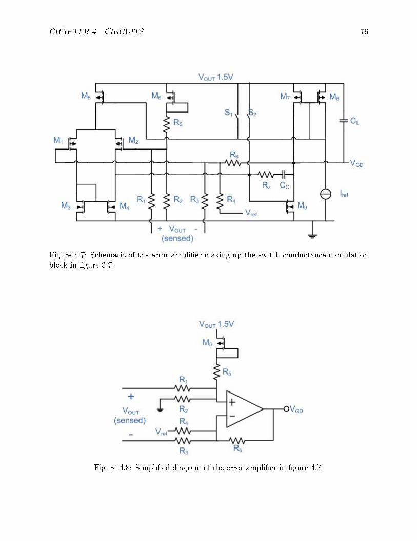
CHAPTER 4. CIRCUITS 76
Figure 4.7: Schematic of the error amplier making up the switch conductance modulationblock in gure 3.7.
Figure 4.8: Simplied diagram of the error amplier in gure 4.7.
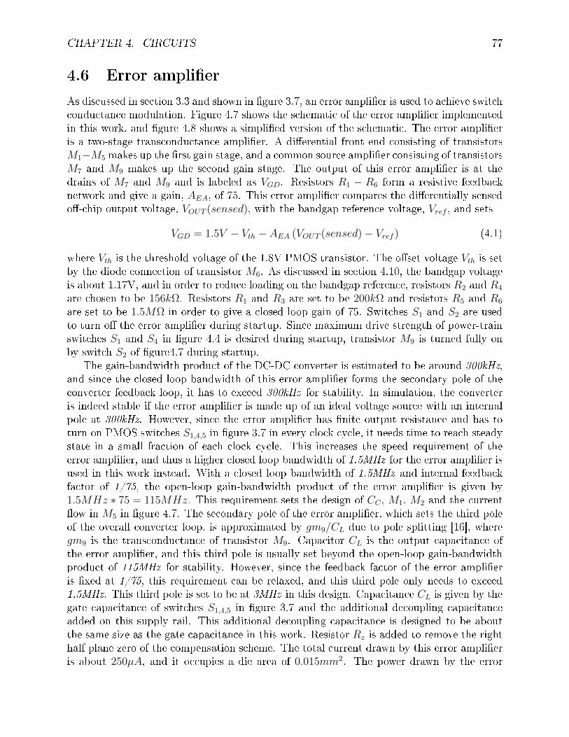
CHAPTER 4. CIRCUITS 77
4.6 Error amplier
As discussed in section 3.3 and shown in gure 3.7, an error amplier is used to achieve switchconductance modulation. Figure 4.7 shows the schematic of the error amplier implementedin this work, and gure 4.8 shows a simplied version of the schematic. The error amplieris a two-stage transconductance amplier. A dierential front end consisting of transistorsM1−M5 makes up the rst gain stage, and a common source amplier consisting of transistorsM7 and M9 makes up the second gain stage. The output of this error amplier is at thedrains of M7 and M9 and is labeled as VGD. Resistors R1 − R6 form a resistive feedbacknetwork and give a gain, AEA, of 75. This error amplier compares the dierentially sensedo-chip output voltage, VOUT (sensed), with the bandgap reference voltage, Vref , and sets
VGD = 1.5V − Vth − AEA (VOUT (sensed)− Vref ) (4.1)
where Vth is the threshold voltage of the 1.8V PMOS transistor. The oset voltage Vth is setby the diode connection of transistor M6. As discussed in section 4.10, the bandgap voltageis about 1.17V, and in order to reduce loading on the bandgap reference, resistors R2 and R4
are chosen to be 156kΩ. Resistors R1 and R3 are set to be 200kΩ and resistors R5 and R6
are set to be 1.5MΩ in order to give a closed loop gain of 75. Switches S1 and S2 are usedto turn o the error amplier during startup. Since maximum drive strength of power-trainswitches S1 and S4 in gure 4.4 is desired during startup, transistor M9 is turned fully onby switch S2 of gure4.7 during startup.
The gain-bandwidth product of the DC-DC converter is estimated to be around 300kHz,and since the closed loop bandwidth of this error amplier forms the secondary pole of theconverter feedback loop, it has to exceed 300kHz for stability. In simulation, the converteris indeed stable if the error amplier is made up of an ideal voltage source with an internalpole at 300kHz. However, since the error amplier has nite output resistance and has toturn on PMOS switches S1,4,5 in gure 3.7 in every clock cycle, it needs time to reach steadystate in a small fraction of each clock cycle. This increases the speed requirement of theerror amplier, and thus a higher closed loop bandwidth of 1.5MHz for the error amplier isused in this work instead. With a closed loop bandwidth of 1.5MHz and internal feedbackfactor of 1/75, the open-loop gain-bandwidth product of the error amplier is given by1.5MHz ∗ 75 = 115MHz. This requirement sets the design of CC , M1, M2 and the currentow in M5 in gure 4.7. The secondary pole of the error amplier, which sets the third poleof the overall converter loop, is approximated by gm9/CL due to pole splitting [16], wheregm9 is the transconductance of transistor M9. Capacitor CL is the output capacitance ofthe error amplier, and this third pole is usually set beyond the open-loop gain-bandwidthproduct of 115MHz for stability. However, since the feedback factor of the error amplieris xed at 1/75, this requirement can be relaxed, and this third pole only needs to exceed1.5MHz. This third pole is set to be at 3MHz in this design. Capacitance CL is given by thegate capacitance of switches S1,4,5 in gure 3.7 and the additional decoupling capacitanceadded on this supply rail. This additional decoupling capacitance is designed to be aboutthe same size as the gate capacitance in this work. Resistor Rz is added to remove the righthalf plane zero of the compensation scheme. The total current drawn by this error amplieris about 250µA, and it occupies a die area of 0.015mm2. The power drawn by the error
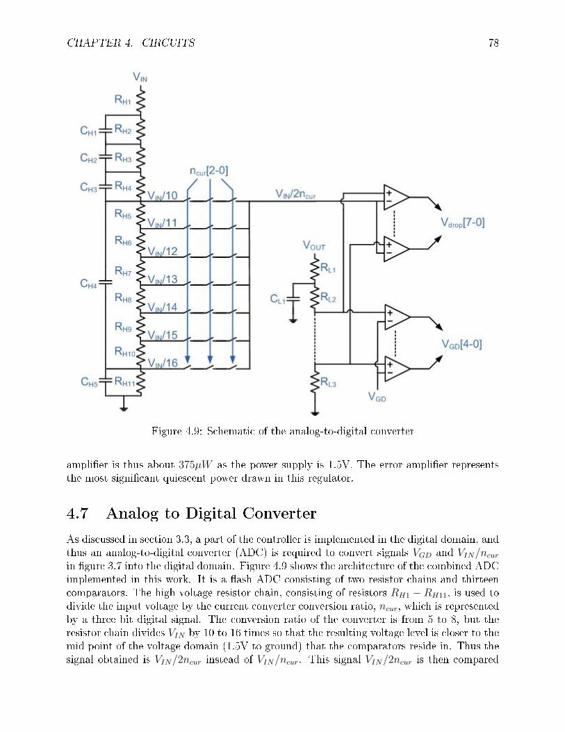
CHAPTER 4. CIRCUITS 78
Figure 4.9: Schematic of the analog-to-digital converter
amplier is thus about 375µW as the power supply is 1.5V. The error amplier representsthe most signicant quiescent power drawn in this regulator.
4.7 Analog to Digital Converter
As discussed in section 3.3, a part of the controller is implemented in the digital domain, andthus an analog-to-digital converter (ADC) is required to convert signals VGD and VIN/ncurin gure 3.7 into the digital domain. Figure 4.9 shows the architecture of the combined ADCimplemented in this work. It is a ash ADC consisting of two resistor chains and thirteencomparators. The high voltage resistor chain, consisting of resistors RH1 −RH11, is used todivide the input voltage by the current converter conversion ratio, ncur, which is representedby a three bit digital signal. The conversion ratio of the converter is from 5 to 8, but theresistor chain divides VIN by 10 to 16 times so that the resulting voltage level is closer to themid point of the voltage domain (1.5V to ground) that the comparators reside in. Thus thesignal obtained is VIN/2ncur instead of VIN/ncur. This signal VIN/2ncur is then compared
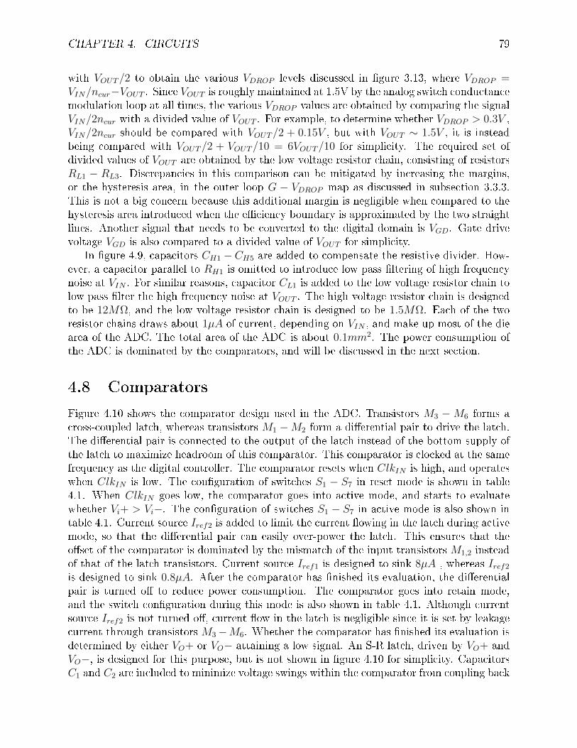
CHAPTER 4. CIRCUITS 79
with VOUT/2 to obtain the various VDROP levels discussed in gure 3.13, where VDROP =VIN/ncur−VOUT . Since VOUT is roughly maintained at 1.5V by the analog switch conductancemodulation loop at all times, the various VDROP values are obtained by comparing the signalVIN/2ncur with a divided value of VOUT . For example, to determine whether VDROP > 0.3V ,VIN/2ncur should be compared with VOUT/2 + 0.15V , but with VOUT ∼ 1.5V , it is insteadbeing compared with VOUT/2 + VOUT/10 = 6VOUT/10 for simplicity. The required set ofdivided values of VOUT are obtained by the low voltage resistor chain, consisting of resistorsRL1 − RL3. Discrepancies in this comparison can be mitigated by increasing the margins,or the hysteresis area, in the outer loop G − VDROP map as discussed in subsection 3.3.3.This is not a big concern because this additional margin is negligible when compared to thehysteresis area introduced when the eciency boundary is approximated by the two straightlines. Another signal that needs to be converted to the digital domain is VGD. Gate drivevoltage VGD is also compared to a divided value of VOUT for simplicity.
In gure 4.9, capacitors CH1 −CH5 are added to compensate the resistive divider. How-ever, a capacitor parallel to RH1 is omitted to introduce low pass ltering of high frequencynoise at VIN . For similar reasons, capacitor CL1 is added to the low voltage resistor chain tolow pass lter the high frequency noise at VOUT . The high voltage resistor chain is designedto be 12MΩ, and the low voltage resistor chain is designed to be 1.5MΩ. Each of the tworesistor chains draws about 1µA of current, depending on VIN , and make up most of the diearea of the ADC. The total area of the ADC is about 0.1mm2. The power consumption ofthe ADC is dominated by the comparators, and will be discussed in the next section.
4.8 Comparators
Figure 4.10 shows the comparator design used in the ADC. Transistors M3 −M6 forms across-coupled latch, whereas transistors M1 −M2 form a dierential pair to drive the latch.The dierential pair is connected to the output of the latch instead of the bottom supply ofthe latch to maximize headroom of this comparator. This comparator is clocked at the samefrequency as the digital controller. The comparator resets when ClkIN is high, and operateswhen ClkIN is low. The conguration of switches S1 − S7 in reset mode is shown in table4.1. When ClkIN goes low, the comparator goes into active mode, and starts to evaluatewhether Vi+ > Vi−. The conguration of switches S1 − S7 in active mode is also shown intable 4.1. Current source Iref2 is added to limit the current owing in the latch during activemode, so that the dierential pair can easily over-power the latch. This ensures that theoset of the comparator is dominated by the mismatch of the input transistors M1,2 insteadof that of the latch transistors. Current source Iref1 is designed to sink 8µA , whereas Iref2is designed to sink 0.8µA. After the comparator has nished its evaluation, the dierentialpair is turned o to reduce power consumption. The comparator goes into retain mode,and the switch conguration during this mode is also shown in table 4.1. Although currentsource Iref2 is not turned o, current ow in the latch is negligible since it is set by leakagecurrent through transistors M3−M6. Whether the comparator has nished its evaluation isdetermined by either VO+ or VO− attaining a low signal. An S-R latch, driven by VO+ andVO−, is designed for this purpose, but is not shown in gure 4.10 for simplicity. CapacitorsC1 and C2 are included to minimize voltage swings within the comparator from coupling back
CHAPTER 4. CIRCUITS 80
Figure 4.10: Schematic of the comparator used in gure 4.9
when S1 S2 S3 S4 S5 S6 S7
Reset mode ClkIN = 1 O O On On O O OnActive mode ClkIN = 0 && done = 0 On On O O On On ORetain mode ClkIN = 0 && done = 1 O On O O O O O
Table 4.1: Switch congurations at dierent modes of the comparator
into the inputs. This is necessary since the inputs are each connected to one of the two highresistance resistor chains, as discussed in section 4.7. Simulation shows that the 3σ osetof this comparator is about 50mV when the input common mode voltage is at 1.2V , and isabout 10mV when the input common voltage is at 0.55V . The oset of the comparator ishigher at higher common mode voltages due to a reduction in dierential pair gain as it goesinto triode operation. As discussed in section 4.7, there are multiple comparators spanninga wide range of voltage levels. For some of these comparators, source followers are addedto levelshift the input signals so that the input common mode voltage is between 0.55V and1.2V.
There are 13 comparators in total in the ADC, and they dominate the power consumptionof the ADC. Total power consumption of the ADC is dependent on VIN , ncur and VGD sincethe comparators turn o after a comparison is made, and the speed of the comparisonis dependent on the input voltage levels. Simulation shows that the ADC, including theresistive dividers, consumes about 35µA of current in most cases, or equivalently, 52.5µWof power.
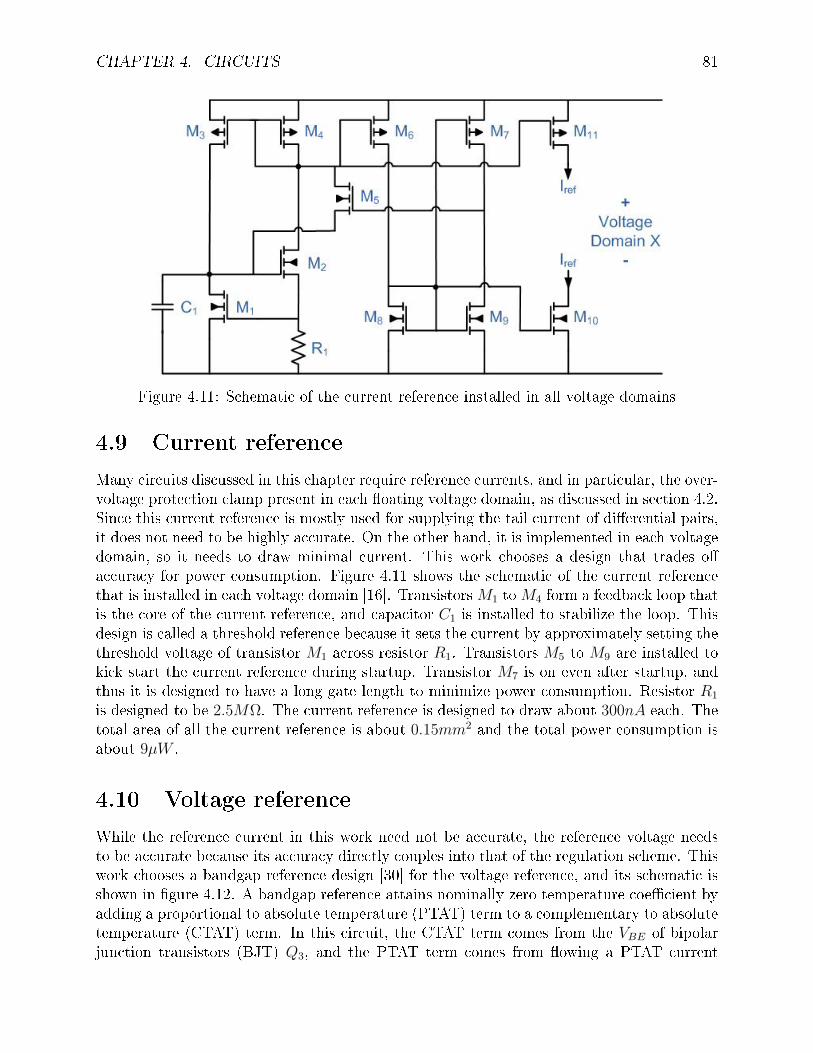
CHAPTER 4. CIRCUITS 81
Figure 4.11: Schematic of the current reference installed in all voltage domains
4.9 Current reference
Many circuits discussed in this chapter require reference currents, and in particular, the over-voltage protection clamp present in each oating voltage domain, as discussed in section 4.2.Since this current reference is mostly used for supplying the tail current of dierential pairs,it does not need to be highly accurate. On the other hand, it is implemented in each voltagedomain, so it needs to draw minimal current. This work chooses a design that trades oaccuracy for power consumption. Figure 4.11 shows the schematic of the current referencethat is installed in each voltage domain [16]. TransistorsM1 toM4 form a feedback loop thatis the core of the current reference, and capacitor C1 is installed to stabilize the loop. Thisdesign is called a threshold reference because it sets the current by approximately setting thethreshold voltage of transistor M1 across resistor R1. Transistors M5 to M9 are installed tokick start the current reference during startup. Transistor M7 is on even after startup, andthus it is designed to have a long gate length to minimize power consumption. Resistor R1
is designed to be 2.5MΩ. The current reference is designed to draw about 300nA each. Thetotal area of all the current reference is about 0.15mm2 and the total power consumption isabout 9µW .
4.10 Voltage reference
While the reference current in this work need not be accurate, the reference voltage needsto be accurate because its accuracy directly couples into that of the regulation scheme. Thiswork chooses a bandgap reference design [30] for the voltage reference, and its schematic isshown in gure 4.12. A bandgap reference attains nominally zero temperature coecient byadding a proportional to absolute temperature (PTAT) term to a complementary to absolutetemperature (CTAT) term. In this circuit, the CTAT term comes from the VBE of bipolarjunction transistors (BJT) Q3, and the PTAT term comes from owing a PTAT current
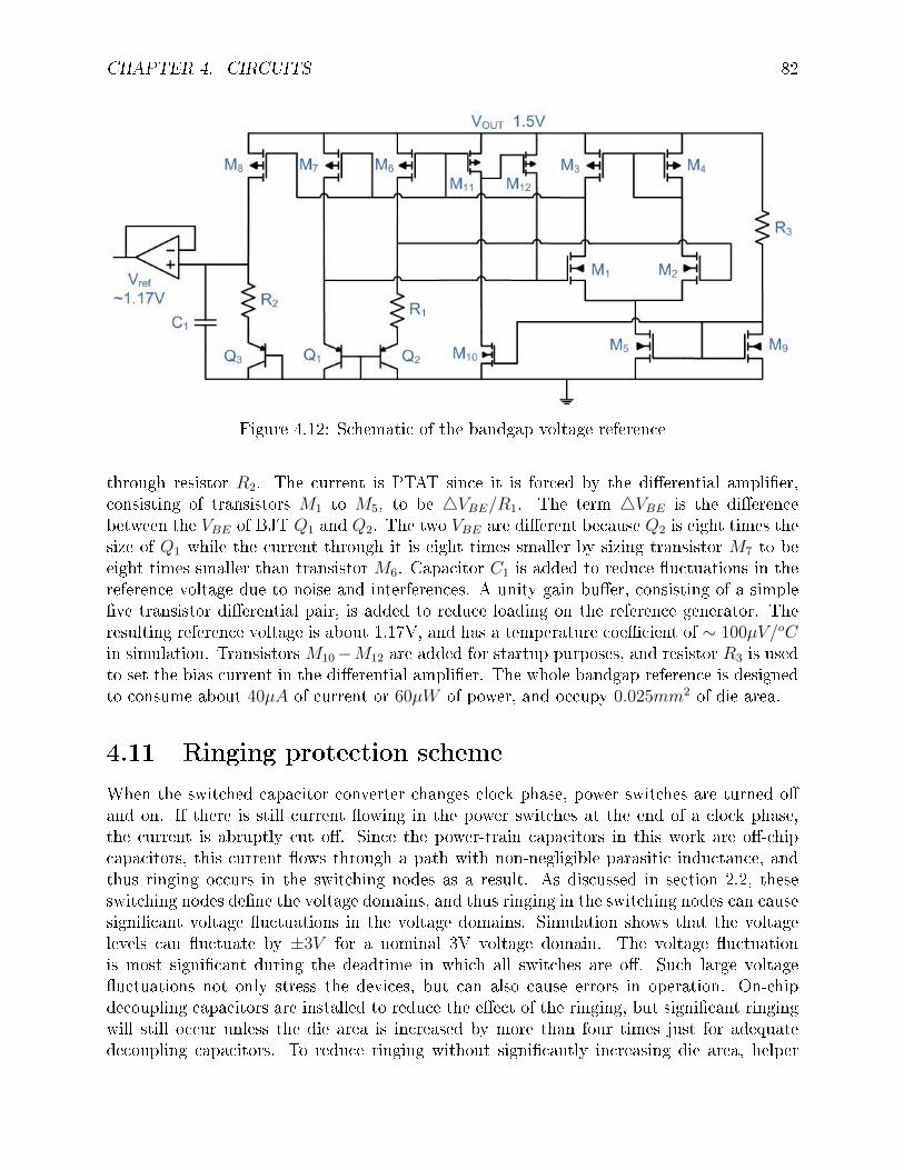
CHAPTER 4. CIRCUITS 82
Figure 4.12: Schematic of the bandgap voltage reference
through resistor R2. The current is PTAT since it is forced by the dierential amplier,consisting of transistors M1 to M5, to be 4VBE/R1. The term 4VBE is the dierencebetween the VBE of BJT Q1 and Q2. The two VBE are dierent because Q2 is eight times thesize of Q1 while the current through it is eight times smaller by sizing transistor M7 to beeight times smaller than transistor M6. Capacitor C1 is added to reduce uctuations in thereference voltage due to noise and interferences. A unity gain buer, consisting of a simpleve transistor dierential pair, is added to reduce loading on the reference generator. Theresulting reference voltage is about 1.17V, and has a temperature coecient of ∼ 100µV/oCin simulation. Transistors M10−M12 are added for startup purposes, and resistor R3 is usedto set the bias current in the dierential amplier. The whole bandgap reference is designedto consume about 40µA of current or 60µW of power, and occupy 0.025mm2 of die area.
4.11 Ringing protection scheme
When the switched capacitor converter changes clock phase, power switches are turned oand on. If there is still current owing in the power switches at the end of a clock phase,the current is abruptly cut o. Since the power-train capacitors in this work are o-chipcapacitors, this current ows through a path with non-negligible parasitic inductance, andthus ringing occurs in the switching nodes as a result. As discussed in section 2.2, theseswitching nodes dene the voltage domains, and thus ringing in the switching nodes can causesignicant voltage uctuations in the voltage domains. Simulation shows that the voltagelevels can uctuate by ±3V for a nominal 3V voltage domain. The voltage uctuationis most signicant during the deadtime in which all switches are o. Such large voltageuctuations not only stress the devices, but can also cause errors in operation. On-chipdecoupling capacitors are installed to reduce the eect of the ringing, but signicant ringingwill still occur unless the die area is increased by more than four times just for adequatedecoupling capacitors. To reduce ringing without signicantly increasing die area, helper
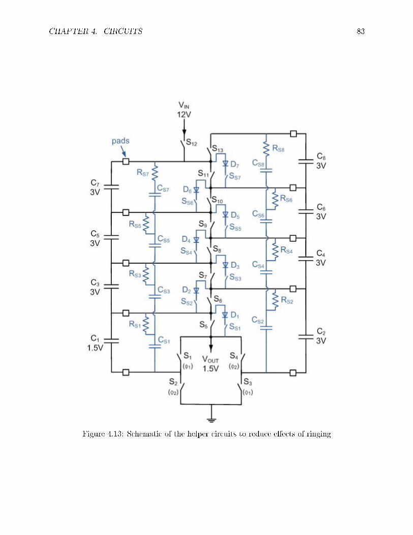
CHAPTER 4. CIRCUITS 83
Figure 4.13: Schematic of the helper circuits to reduce eects of ringing
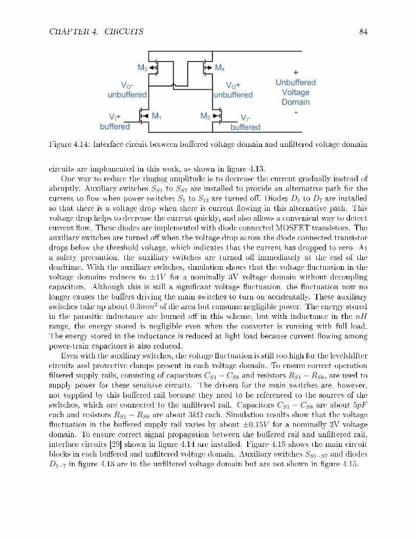
CHAPTER 4. CIRCUITS 84
Figure 4.14: Interface circuit between buered voltage domain and unltered voltage domain
circuits are implemented in this work, as shown in gure 4.13.One way to reduce the ringing amplitude is to decrease the current gradually instead of
abruptly. Auxiliary switches SS1 to SS7 are installed to provide an alternative path for thecurrent to ow when power switches S1 to S13 are turned o. Diodes D1 to D7 are installedso that there is a voltage drop when there is current owing in this alternative path. Thisvoltage drop helps to decrease the current quickly, and also allows a convenient way to detectcurrent ow. These diodes are implemented with diode connected MOSFET transistors. Theauxiliary switches are turned o when the voltage drop across the diode connected transistordrops below the threshold voltage, which indicates that the current has dropped to zero. Asa safety precaution, the auxiliary switches are turned o immediately at the end of thedeadtime. With the auxiliary switches, simulation shows that the voltage uctuation in thevoltage domains reduces to ±1V for a nominally 3V voltage domain without decouplingcapacitors. Although this is still a signicant voltage uctuation, the uctuation now nolonger causes the buers driving the main switches to turn on accidentally. These auxiliaryswitches take up about 0.3mm2 of die area but consume negligible power. The energy storedin the parasitic inductance are burned o in this scheme, but with inductance in the nHrange, the energy stored is negligible even when the converter is running with full load.The energy stored in the inductance is reduced at light load because current owing amongpower-train capacitors is also reduced.
Even with the auxiliary switches, the voltage uctuation is still too high for the levelshiftercircuits and protective clamps present in each voltage domain. To ensure correct operationltered supply rails, consisting of capacitors CS1 −CS8 and resistors RS1 −RS8, are used tosupply power for these sensitive circuits. The drivers for the main switches are, however,not supplied by this buered rail because they need to be referenced to the sources of theswitches, which are connected to the unltered rail. Capacitors CS1 − CS8 are about 5pFeach and resistors RS1 − RS8 are about 3kΩ each. Simulation results show that the voltageuctuation in the buered supply rail varies by about ±0.15V for a nominally 3V voltagedomain. To ensure correct signal propagation between the buered rail and unltered rail,interface circuits [29] shown in gure 4.14 are installed. Figure 4.15 shows the main circuitblocks in each buered and unltered voltage domain. Auxiliary switches SS1−S7 and diodesD1−7 in gure 4.13 are in the unltered voltage domain but are not shown in gure 4.15.
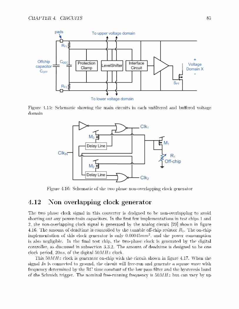
CHAPTER 4. CIRCUITS 85
Figure 4.15: Schematic showing the main circuits in each unltered and buered voltagedomain
Figure 4.16: Schematic of the two phase non-overlapping clock generator
4.12 Non overlapping clock generator
The two phase clock signal in this converter is designed to be non-overlapping to avoidshorting out any power-train capacitors. In the rst few implementations in test chips 1 and2, the non-overlapping clock signal is generated by the analog circuit [29] shown in gure4.16. The amount of deadtime is controlled by the tunable o-chip resistor R1. The on-chipimplementation of this clock generator is only 0.00045mm2, and the power consumptionis also negligible. In the nal test chip, the two-phase clock is generated by the digitalcontroller, as discussed in subsection 3.3.2. The amount of deadtime is designed to be oneclock period, 20ns, of the digital 50MHz clock.
This 50MHz clock is generator on-chip with the circuit shown in gure 4.17. When thesignal In is connected to ground, the circuit will free-run and generate a square wave withfrequency determined by the RC time constant of the low pass lter and the hysteresis bandof the Schmidt trigger. The nominal free-running frequency is 50MHz but can vary by up
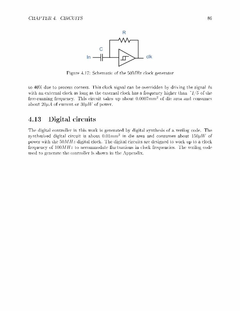
CHAPTER 4. CIRCUITS 86
Figure 4.17: Schematic of the 50MHz clock generator
to 40% due to process corners. This clock signal can be overridden by driving the signal Inwith an external clock as long as the external clock has a frequency higher than ~1/5 of thefree-running frequency. This circuit takes up about 0.0007mm2 of die area and consumesabout 20µA of current or 30µW of power.
4.13 Digital circuits
The digital controller in this work is generated by digital synthesis of a verilog code. Thesynthesized digital circuit is about 0.01mm2 in die area and consumes about 150µW ofpower with the 50MHz digital clock. The digital circuits are designed to work up to a clockfrequency of 100MHz to accommodate uctuations in clock frequencies. The verilog codeused to generate the controller is shown in the Appendix.
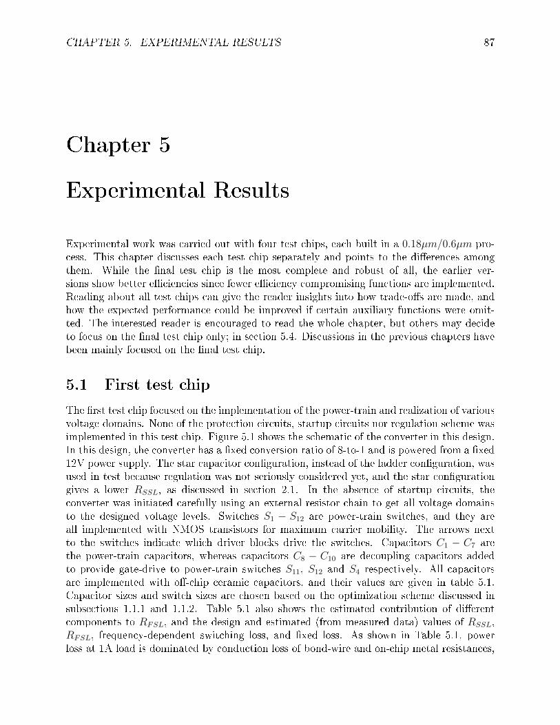
CHAPTER 5. EXPERIMENTAL RESULTS 87
Chapter 5
Experimental Results
Experimental work was carried out with four test chips, each built in a 0.18µm/0.6µm pro-cess. This chapter discusses each test chip separately and points to the dierences amongthem. While the nal test chip is the most complete and robust of all, the earlier ver-sions show better eciencies since fewer eciency compromising functions are implemented.Reading about all test chips can give the reader insights into how trade-os are made, andhow the expected performance could be improved if certain auxiliary functions were omit-ted. The interested reader is encouraged to read the whole chapter, but others may decideto focus on the nal test chip only; in section 5.4. Discussions in the previous chapters havebeen mainly focused on the nal test chip.
5.1 First test chip
The rst test chip focused on the implementation of the power-train and realization of variousvoltage domains. None of the protection circuits, startup circuits nor regulation scheme wasimplemented in this test chip. Figure 5.1 shows the schematic of the converter in this design.In this design, the converter has a xed conversion ratio of 8-to-1 and is powered from a xed12V power supply. The star capacitor conguration, instead of the ladder conguration, wasused in test because regulation was not seriously considered yet, and the star congurationgives a lower RSSL, as discussed in section 2.1. In the absence of startup circuits, theconverter was initiated carefully using an external resistor chain to get all voltage domainsto the designed voltage levels. Switches S1 − S12 are power-train switches, and they areall implemented with NMOS transistors for maximum carrier mobility. The arrows nextto the switches indicate which driver blocks drive the switches. Capacitors C1 − C7 arethe power-train capacitors, whereas capacitors C8 − C10 are decoupling capacitors addedto provide gate-drive to power-train switches S11, S12 and S4 respectively. All capacitorsare implemented with o-chip ceramic capacitors, and their values are given in table 5.1.Capacitor sizes and switch sizes are chosen based on the optimization scheme discussed insubsections 1.1.1 and 1.1.2. Table 5.1 also shows the estimated contribution of dierentcomponents to RFSL, and the design and estimated (from measured data) values of RSSL,RFSL, frequency-dependent switching loss, and xed loss. As shown in Table 5.1, powerloss at 1A load is dominated by conduction loss of bond-wire and on-chip metal resistances,
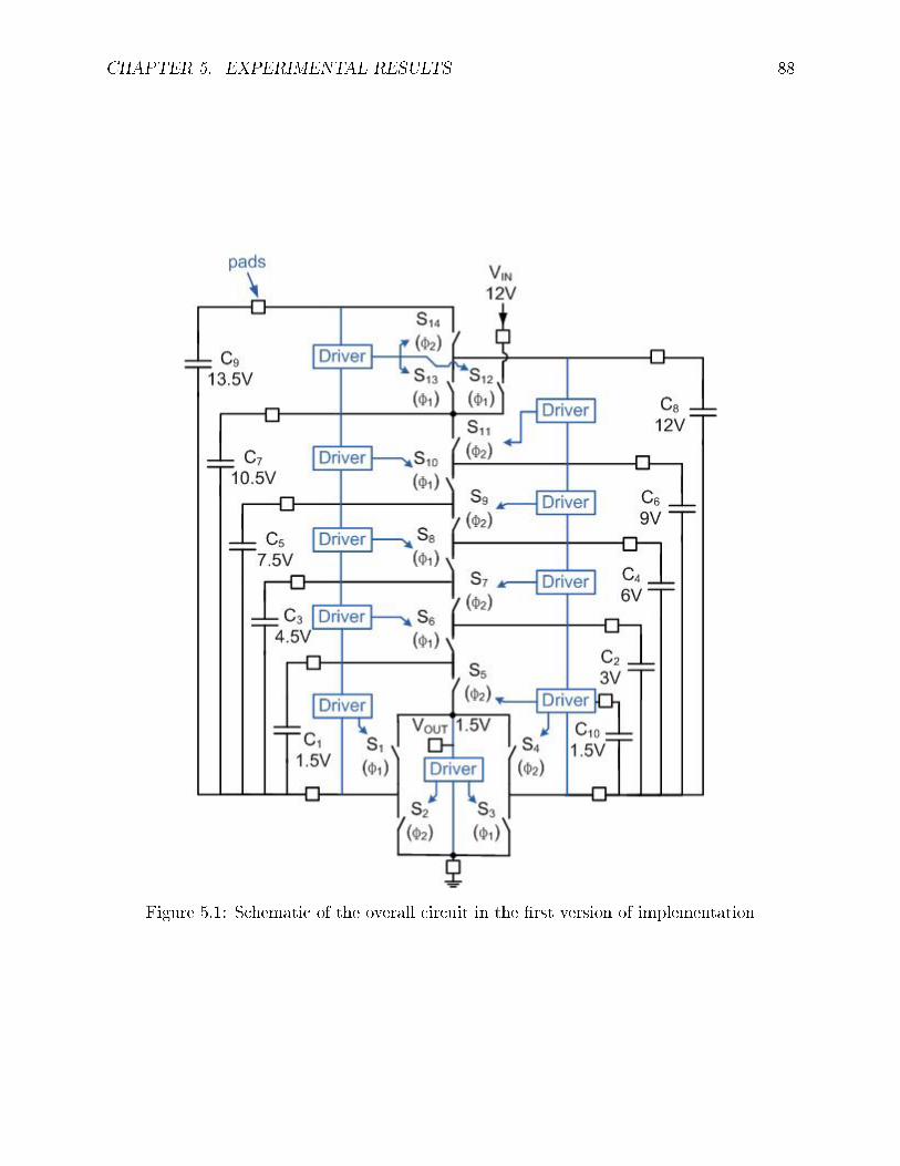
CHAPTER 5. EXPERIMENTAL RESULTS 88
Figure 5.1: Schematic of the overall circuit in the rst version of implementation
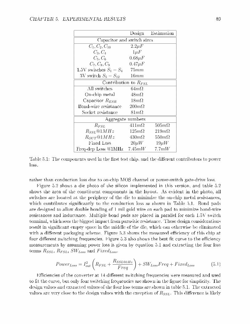
CHAPTER 5. EXPERIMENTAL RESULTS 89
Design Estimation
Capacitor and switch sizesC1, C2, C10 2.2µFC3, C4 1µFC5, C6 0.68µF
C7, C8, C9 0.47µF1.5V switches S1 − S4 75mm3V switch S5 − S12 16mm
Contribution to RFSL
All switches 64mΩOn-chip metal 48mΩCapacitor RESR 18mΩ
Bond-wire resistance 200mΩSocket resistance 81mΩ
Aggregate numbersRFSL 411mΩ 505mΩ
RSSL@1MHz 125mΩ 219mΩROUT@1MHz 430mΩ 550mΩFixed Loss 20µW 19µW
Freq-dep Loss @1MHz 7.45mW 7.7mW
Table 5.1: The components used in the rst test chip, and the dierent contributors to powerloss.
rather than conduction loss due to on-chip MOS channel or power-switch gate-drive loss.Figure 5.2 shows a die photo of the silicon implemented in this version, and table 5.2
shows the area of the constituent components in the layout. As evident in the photo, allswitches are located at the periphery of the die to minimize the on-chip metal resistances,which contributes signicantly to the conduction loss as shown in Table 5.1. Bond padsare designed to allow double bonding of 1 mil gold wire on each pad to minimize bond-wireresistances and inductance. Multiple bond pads are placed in parallel for each 1.5V switchterminal, which sees the biggest impact from parasitic resistance. These design considerationsresult in signicant empty space in the middle of the die, which can otherwise be eliminatedwith a dierent packaging scheme. Figure 5.3 shows the measured eciency of this chip atfour dierent switching frequencies. Figure 5.3 also shows the best t curve to the eciencymeasurements by assuming power loss is given by equation 5.1 and extracting the four lossterms RSSL, RFSL, SWLoss and FixedLoss.
PowerLoss = I2out
(RFSL +
RSSL@1Hz
Freq
)+ SWLossFreq + FixedLoss (5.1)
Eciencies of the converter at 14 dierent switching frequencies were measured and usedto t the curve, but only four switching frequencies are shown in the gure for simplicity. Thedesign values and extracted values of the four loss terms are shown in table 5.1. The extractedvalues are very close to the design values with the exception of RSSL. This dierence is likely
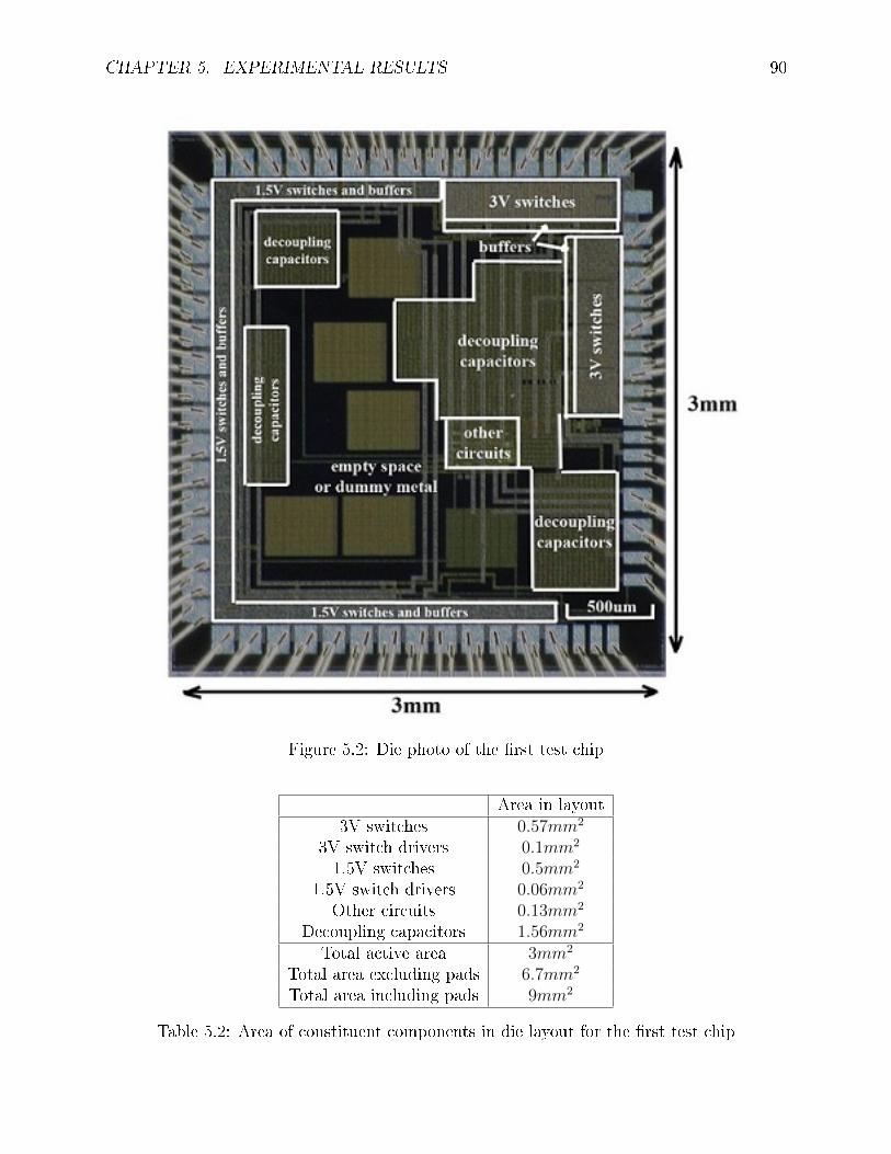
CHAPTER 5. EXPERIMENTAL RESULTS 90
Figure 5.2: Die photo of the rst test chip
Area in layout3V switches 0.57mm2
3V switch drivers 0.1mm2
1.5V switches 0.5mm2
1.5V switch drivers 0.06mm2
Other circuits 0.13mm2
Decoupling capacitors 1.56mm2
Total active area 3mm2
Total area excluding pads 6.7mm2
Total area including pads 9mm2
Table 5.2: Area of constituent components in die layout for the rst test chip
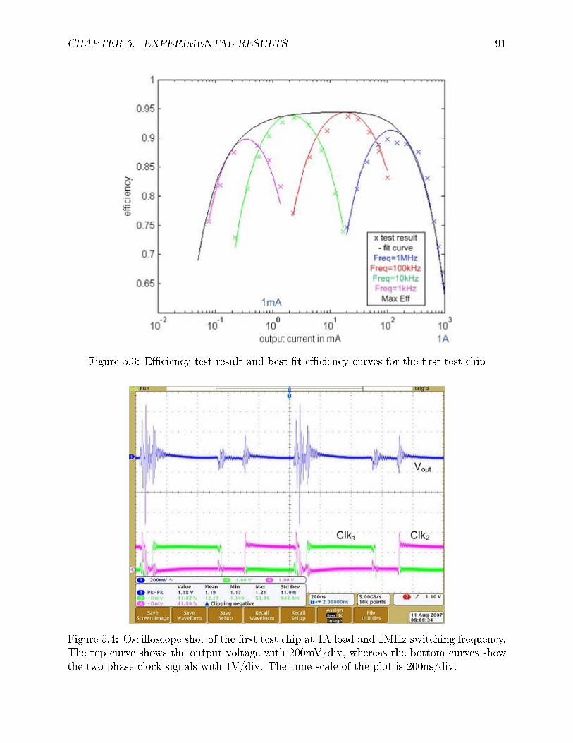
CHAPTER 5. EXPERIMENTAL RESULTS 91
Figure 5.3: Eciency test result and best t eciency curves for the rst test chip
Figure 5.4: Oscilloscope shot of the rst test chip at 1A load and 1MHz switching frequency.The top curve shows the output voltage with 200mV/div, whereas the bottom curves showthe two phase clock signals with 1V/div. The time scale of the plot is 200ns/div.
CHAPTER 5. EXPERIMENTAL RESULTS 92
Area in layout3V switches 0.57mm2
3V switch drivers 0.1mm2
1.5V switches 0.5mm2
1.5V switch drivers 0.06mm2
Other circuits 0.25mm2
Decoupling capacitors 1.56mm2
Total active area 3mm2
Total area excluding pads 6.7mm2
Total area including pads 9mm2
Table 5.3: Area of various components in die layout for the second test chip
due to eective capacitance of ceramic capacitance being considerably smaller than statedvalues when a voltage bias is present. Figure 5.3 also shows the highest eciency over a rangeof output current levels if switching frequency is optimized by equation 2.1. The converterachieves a very high eciency over a very wide range of output current levels. Figure 5.4shows an oscilloscope shot of the output voltage when the converter is operating at 1A loadcurrent with a switching frequency of 1MHz. The oscilloscope plot shows the two phase clocksignal with a signicant deadtime in between. This deadtime of about 180ns was requiredbecause the levelshifter circuit used was a design[31] that works considerably slower thanthe one discussed in section 4.1. The result and design of this test chip has been discussedin the master thesis [32], but the test data has since been rened, as reported here.
5.2 Second test chip
The second test chip focused on making the converter more robust. The levelshifter circuitwas improved, and protection circuits and startup circuits were added. Figure 5.5 showsthe die photo of this version of this test chip, and table 5.3 shows the sizes of the layoutcomponents. The die layout is basically the same as in the rst implementation, with theexception that the other circuit block is larger. Figure 5.6 shows the measured eciency ofthe chip at two dierent switching frequencies and the respective best-t curves. Ecienciesof the converter at seven dierent switching frequencies were measured and used to t thecurve, but only two switching frequencies are shown in the gure for simplicity. The designvalues and extracted values of the four loss terms are shown in table 5.4. Figure 5.7 showsan oscilloscope shot of the output voltage and the two phase clock signal at 230mA loadcurrent with a switching frequency of 1MHz. Figure 5.8 shows the voltage levels on fourpower-train capacitors during startup.
When compared with the rst test chip results, the second test chip sees the biggestimprovement in reducing RFSL. This is because with the chip robustness signicantly im-proved, the test socket and the package can be removed. The chip is directly bonded ontothe printed circuit board (PCB), and this allows a reduction in bondwire length and bond-wire parasitic resistance. With the improvement to the levelshifter circuits, the deadtimebetween the two phase clock signals is reduced, as evident in gure 5.7. This allows a reduc-
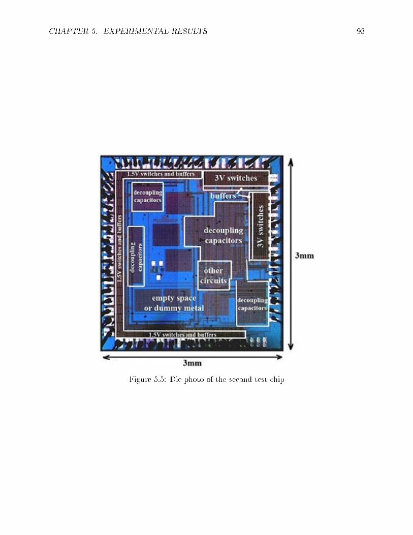
CHAPTER 5. EXPERIMENTAL RESULTS 93
Figure 5.5: Die photo of the second test chip
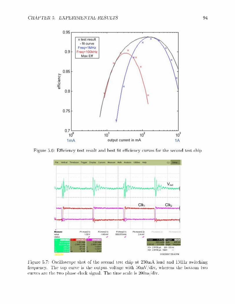
CHAPTER 5. EXPERIMENTAL RESULTS 94
Figure 5.6: Eciency test result and best t eciency curves for the second test chip
Figure 5.7: Oscilloscope shot of the second test chip at 230mA load and 1MHz switchingfrequency. The top curve is the output voltage with 50mV/div, whereas the bottom twocurves are the two phase clock signal. The time scale is 200ns/div.
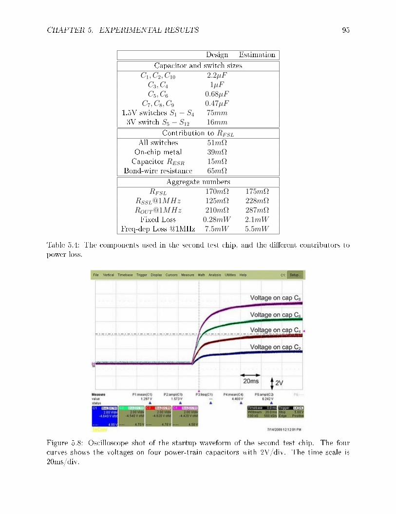
CHAPTER 5. EXPERIMENTAL RESULTS 95
Design Estimation
Capacitor and switch sizesC1, C2, C10 2.2µFC3, C4 1µFC5, C6 0.68µF
C7, C8, C9 0.47µF1.5V switches S1 − S4 75mm3V switch S5 − S12 16mm
Contribution to RFSL
All switches 51mΩOn-chip metal 39mΩCapacitor RESR 15mΩ
Bond-wire resistance 65mΩ
Aggregate numbersRFSL 170mΩ 175mΩ
RSSL@1MHz 125mΩ 228mΩROUT@1MHz 210mΩ 287mΩFixed Loss 0.28mW 2.1mW
Freq-dep Loss @1MHz 7.5mW 5.5mW
Table 5.4: The components used in the second test chip, and the dierent contributors topower loss.
Figure 5.8: Oscilloscope shot of the startup waveform of the second test chip. The fourcurves shows the voltages on four power-train capacitors with 2V/div. The time scale is20ms/div.
CHAPTER 5. EXPERIMENTAL RESULTS 96
tion in the contribution of switch resistances, on-chip metal resistances and capacitor ESRto RFSL. This reduction is due to an increase in duty ratio, Dj, in equation 1.6 even thoughthe resistances remain the same.
There are two main design shortcomings in implementation for this test chip. The rstone is the protection clamp circuits turned on unexpectedly by capacitive coupling intosensitive nodes as explained in section 4.2. This caused the xed loss, as shown in table5.4, to be signicantly higher than expected. To solve this problem, capacitor C1 in gure4.3 was added to all subsequent implementation versions. Another error in this test chipwas in the sizing of the startup helper circuits. The startup helper circuits were sized toosmall, and this caused the converter to startup in 40ms instead of a designed value of 200µs.This has also been diagnosed and xed in subsequent implementations. The results of thisimplementation have been published in [33] and [34].
5.3 Third test chip
The third test chip focused on reducing power loss, and realization of a multi-conversion-ratio topology. Figure 5.9 shows the schematic of the converter in this test chip. Theconverter utilized the integer-step multi-conversion-ratio topology discussed in subsection2.4.1. When compared with previous implementations, some of the power-train transistorswere changed from NMOS transistors to PMOS transistors to reduce the number of voltagedomains. This results in eliminating capacitors C9 and C10 in gure 5.1 and a reduction inpin-counts. Choice of capacitors were switched from minimizing total ΣCV 2 of the capacitorsto using the 0603 ceramic capacitor with highest capacitance, as discussed in subsection 2.3.1.Optimization of switches used the algorithm discussed in subsection 2.3.2, but with multipleconversion ratios, the switch sizes are chosen such that RFSL is similar for the four dierentconversion ratios. In terms of packaging, ip-chip bonding was used in placed of bondwiresto eliminate bondwire resistances and to reduce on-chip metal resistances. These resistanceswere main contributors to RFSL, and reducing them would allow the converter to attainhigher eciencies and/or operate at higher load current levels.
Table 5.5 shows the components used, and the expected loss factors. Figure 5.10 shows thedie photo and table 5.6 shows the area of layout components. By using ipchip packaging, theempty space in previous versions is eliminated, and this allows the converter to attain higherperformance with an overall shrink in die size. Figure 5.11 shows the expected eciency atvarious switching frequencies at a xed conversion ratio of 8-to-1. The converter is expectedto attain a higher peak eciency, and also exhibit high eciency over a wider range of loadcurrents when compared to previous test chips. Unfortunately, the dies were manufacturedand diced without being bumped. Numerous attempts were made to package the chip butwithout success. As a result, the expected results of this chip cannot be veried and thenext test chip reverted back to bondwires to avoid repeating this problem. The expectedresult of this chip has been published in [34].
Although regulation was not implemented in this test chip, it is interesting to investigatethe expected eciency of the converter if the regulation scheme discussed in chapter 3 hadbeen implemented. This will show the change in expected eciency if having VOUT tightlyregulated is more important than converter eciency, as in the case of most dc-dc converters.
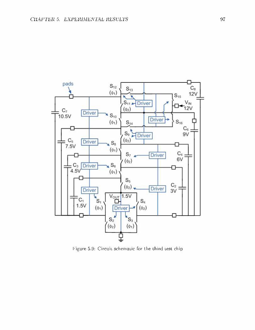
CHAPTER 5. EXPERIMENTAL RESULTS 97
Figure 5.9: Circuit schematic for the third test chip
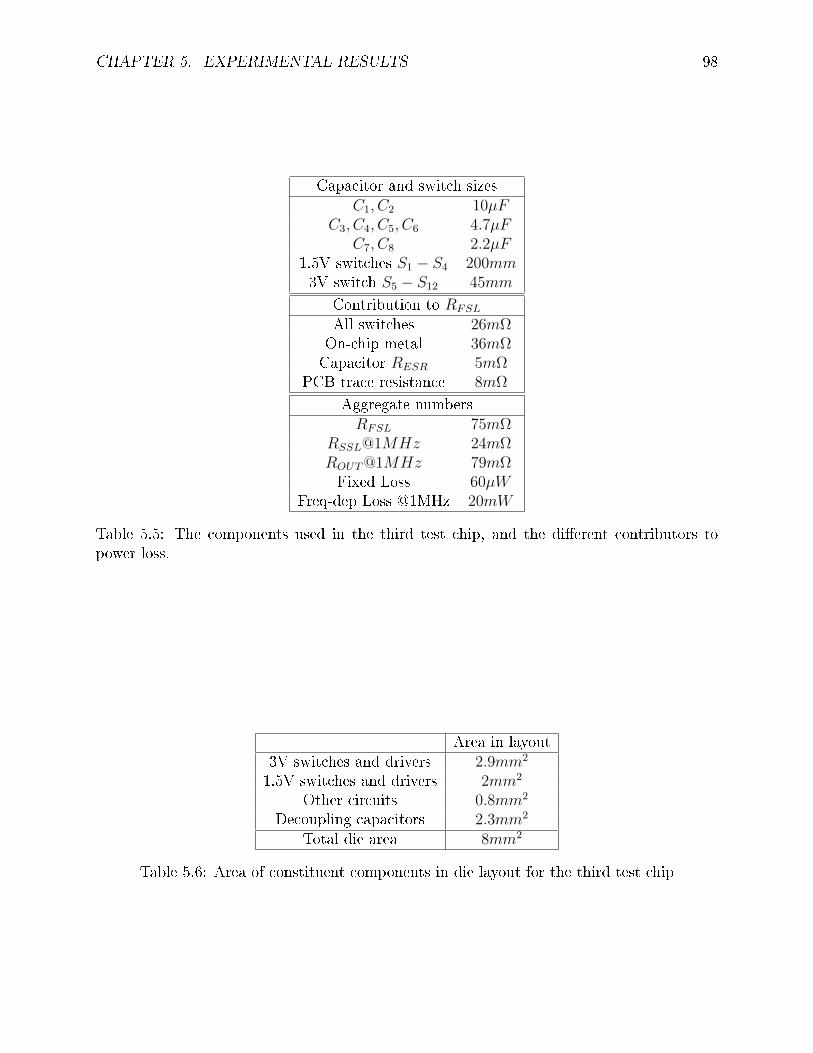
CHAPTER 5. EXPERIMENTAL RESULTS 98
Capacitor and switch sizesC1, C2 10µF
C3, C4, C5, C6 4.7µFC7, C8 2.2µF
1.5V switches S1 − S4 200mm3V switch S5 − S12 45mm
Contribution to RFSL
All switches 26mΩOn-chip metal 36mΩCapacitor RESR 5mΩ
PCB trace resistance 8mΩ
Aggregate numbersRFSL 75mΩ
RSSL@1MHz 24mΩROUT@1MHz 79mΩFixed Loss 60µW
Freq-dep Loss @1MHz 20mW
Table 5.5: The components used in the third test chip, and the dierent contributors topower loss.
Area in layout3V switches and drivers 2.9mm2
1.5V switches and drivers 2mm2
Other circuits 0.8mm2
Decoupling capacitors 2.3mm2
Total die area 8mm2
Table 5.6: Area of constituent components in die layout for the third test chip
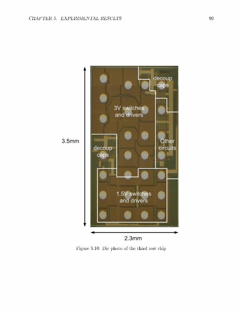
CHAPTER 5. EXPERIMENTAL RESULTS 99
Figure 5.10: Die photo of the third test chip
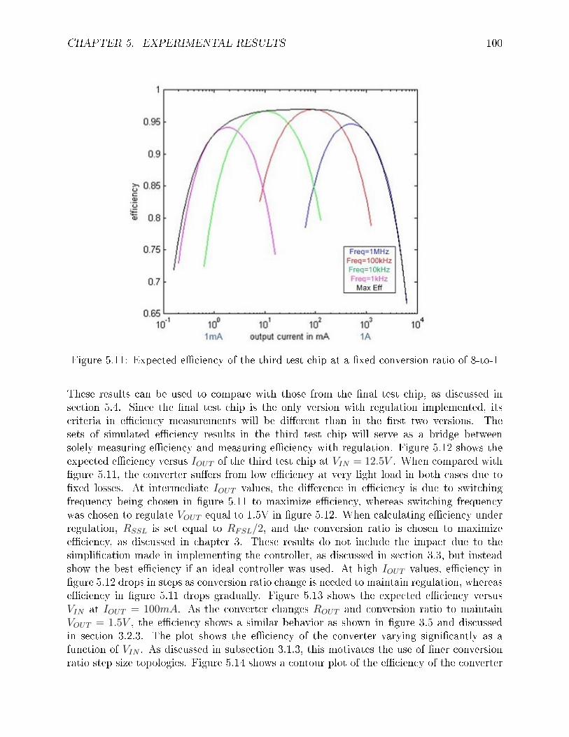
CHAPTER 5. EXPERIMENTAL RESULTS 100
Figure 5.11: Expected eciency of the third test chip at a xed conversion ratio of 8-to-1
These results can be used to compare with those from the nal test chip, as discussed insection 5.4. Since the nal test chip is the only version with regulation implemented, itscriteria in eciency measurements will be dierent than in the rst two versions. Thesets of simulated eciency results in the third test chip will serve as a bridge betweensolely measuring eciency and measuring eciency with regulation. Figure 5.12 shows theexpected eciency versus IOUT of the third test chip at VIN = 12.5V . When compared withgure 5.11, the converter suers from low eciency at very light load in both cases due toxed losses. At intermediate IOUT values, the dierence in eciency is due to switchingfrequency being chosen in gure 5.11 to maximize eciency, whereas switching frequencywas chosen to regulate VOUT equal to 1.5V in gure 5.12. When calculating eciency underregulation, RSSL is set equal to RFSL/2, and the conversion ratio is chosen to maximizeeciency, as discussed in chapter 3. These results do not include the impact due to thesimplication made in implementing the controller, as discussed in section 3.3, but insteadshow the best eciency if an ideal controller was used. At high IOUT values, eciency ingure 5.12 drops in steps as conversion ratio change is needed to maintain regulation, whereaseciency in gure 5.11 drops gradually. Figure 5.13 shows the expected eciency versusVIN at IOUT = 100mA. As the converter changes ROUT and conversion ratio to maintainVOUT = 1.5V , the eciency shows a similar behavior as shown in gure 3.5 and discussedin section 3.2.3. The plot shows the eciency of the converter varying signicantly as afunction of VIN . As discussed in subsection 3.1.3, this motivates the use of ner conversionratio step size topologies. Figure 5.14 shows a contour plot of the eciency of the converter
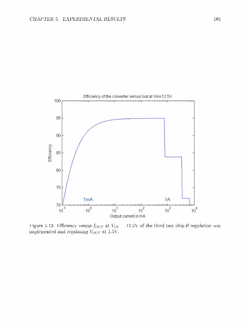
CHAPTER 5. EXPERIMENTAL RESULTS 101
Figure 5.12: Eciency versus IOUT at VIN = 12.5V of the third test chip if regulation wasimplemented and regulating VOUT at 1.5V.
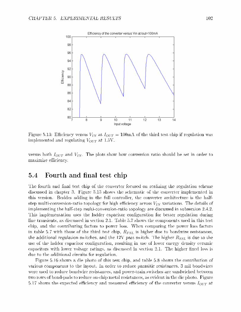
CHAPTER 5. EXPERIMENTAL RESULTS 102
Figure 5.13: Eciency versus VIN at IOUT = 100mA of the third test chip if regulation wasimplemented and regulating VOUT at 1.5V.
versus both IOUT and VIN . The plots show how conversion ratio should be set in order tomaximize eciency.
5.4 Fourth and nal test chip
The fourth and nal test chip of the converter focused on realizing the regulation schemediscussed in chapter 3. Figure 5.15 shows the schematic of the converter implemented inthis version. Besides adding in the full controller, the converter architecture is the half-step multi-conversion-ratio topology for high eciency across VIN variations. The details ofimplementing the half-step multi-conversion-ratio topology are discussed in subsection 2.4.2.This implementation uses the ladder capacitor conguration for better regulation duringline transients, as discussed in section 2.1. Table 5.7 shows the components used in this testchip, and the contributing factors to power loss. When comparing the power loss factorsin table 5.7 with those of the third test chip, RFSL is higher due to bondwire resistances,the additional regulation switches, and the 12V pass switch. The higher RSSL is due to theuse of the ladder capacitor conguration, resulting in use of lower energy density ceramiccapacitors with lower voltage ratings, as discussed in section 2.1. The higher xed loss isdue to the additional circuits for regulation.
Figure 5.16 shows a die photo of this test chip, and table 5.8 shows the contribution ofvarious components to the layout. In order to reduce parasitic resistances, 3 mil bondwireswere used to reduce bondwire resistances, and power-train switches are sandwiched betweentwo rows of bond-pads to reduce on-chip metal resistances, as evident in the die photo. Figure5.17 shows the expected eciency and measured eciency of the converter versus IOUT at
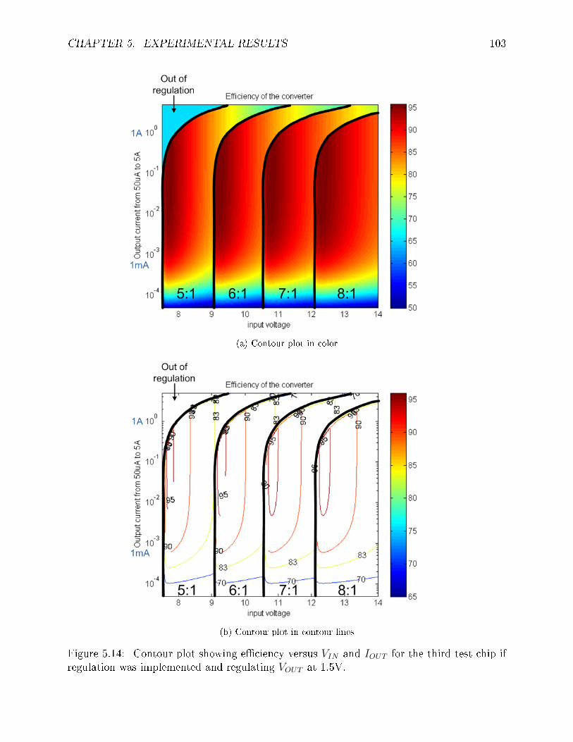
CHAPTER 5. EXPERIMENTAL RESULTS 103
(a) Contour plot in color
(b) Contour plot in contour lines
Figure 5.14: Contour plot showing eciency versus VIN and IOUT for the third test chip ifregulation was implemented and regulating VOUT at 1.5V.
CHAPTER 5. EXPERIMENTAL RESULTS 104
around VIN = 8.7V . The dierence between expected eciency and measured eciency canbe due to RSSL being xed at RFSL/2 when calculating expected eciency, but in reality thisratio can vary signicantly due to the approximation used in the frequency loop, as discussedin subsection 3.3.2. Figure 5.18 shows the expected eciency and measured eciency of theconverter versus VIN at around IOUT = 50mA and IOUT = 220mA. When compared withgure 5.13 of the third test chip, gure 5.18 shows signicant improvement in eciencyvariations across VIN due to the availability of ner conversion ratio step size. Figure 5.19shows the contour plot of the expected eciency of the converter versus both IOUT and VIN .
In terms of load transients, gure 5.20 shows the behavior of the converter during loadingand unloading steps of IOUT = 150mA at VIN = 13V . In this case, the converter maintainsregulation by changing switch conductance and switching frequency, but without changingconversion ratio. The gate drive signal in the gure is VGD in gure 3.7 discussed in section3.3. As evident in gure 5.20, the gate drive signal, VGD, closely resembles VOUT and reectsthe behavior of the error amplier discussed in subsection 3.3.1. As evident from the gatedrive signal, VGD, the converter changes clock phase at a particular value of VGD. Thisbehavior represents the lower-bound hysteretic control behavior in determining switchingfrequency, as expected from the frequency controller discussed in subsection 3.3.2. As evidentin gure 5.20, the inner loop controller maintains VOUT to be within a 20mV band duringthis load and unloading transient.
Figure 5.21 shows the behavior of the converter with an IOUT = 1A loading and un-loading step at VIN = 9V . In this case, one step change in conversion ratio is needed tomaintain regulation. When the loading step occurs, VOUT drops and causes a reduction inthe conversion ratio from 5.5-to-1 to 5-to-1, as evident by the least signicant bit (LSB) ofthe conversion ratio shown in the gure. This conversion ratio change causes VOUT to riseback up to roughly the original level and maintain regulation. Conversely, the unloadingstep causes VOUT to rise immediately, and causes the conversion ratio to increase back from5-to-1 to 5.5-to-1. This quick increase in conversion ratio is due to the converter enteringregion E in the G − VDROP control space shown in gure 3.13, and discussed in subsection3.3.3. As shown by the clock signal in the gure, despite the same IOUT level, the switchingfrequency after the unloading step is lower than before the loading step. This is due to theavailable stored charge in the ying capacitors after the unloading transient. The storedcharge allows the converter to maintain regulation with lower conductance. As the storedcharge is drained away slowly by IOUT = 10mA, the converter eventually reaches the samestate as before the loading step. These behaviors match the simulation results shown insubsection 3.3.5, and conrm the performance of the outer loop conversion ratio controllerdiscussed in subsection 3.3.3. As shown in the gure, the peak to peak variation in VOUT isless than 30mV in this full loading and unloading step.
Figure 5.22 shows a loading and unloading transient in which two steps of change inconversion ratio are needed. As shown in the gure, the converter rst changed from aconversion ratio of 6-to-1 to 5.5-to-1. However, this conversion ratio change was not enough,and VOUT continued to drop. The converter then changed to a conversion ratio of 5-to-1 shortly after. The output voltage, VOUT , then rose and settled at roughly the originalvoltage level before the loading transient. Although the converter experienced the sameoutput current step in both gure 5.21 and gure 5.22, the number of conversion ratiochange was not the same because the input voltage and initial condition of the converter
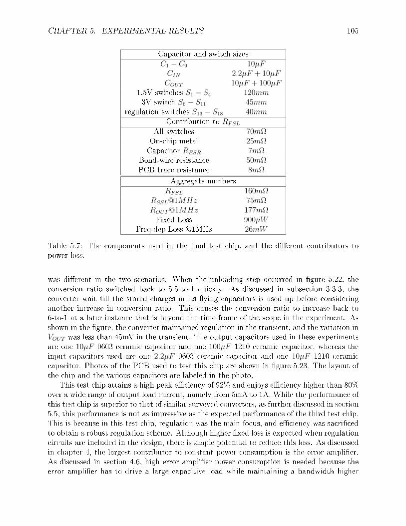
CHAPTER 5. EXPERIMENTAL RESULTS 105
Capacitor and switch sizesC1 − C9 10µFCIN 2.2µF + 10µFCOUT 10µF + 100µF
1.5V switches S1 − S4 120mm3V switch S6 − S11 45mm
regulation switches S13 − S18 40mmContribution to RFSL
All switches 70mΩOn-chip metal 25mΩCapacitor RESR 7mΩ
Bond-wire resistance 50mΩPCB trace resistance 8mΩ
Aggregate numbersRFSL 160mΩ
RSSL@1MHz 75mΩROUT@1MHz 177mΩFixed Loss 900µW
Freq-dep Loss @1MHz 26mW
Table 5.7: The components used in the nal test chip, and the dierent contributors topower loss.
was dierent in the two scenarios. When the unloading step occurred in gure 5.22, theconversion ratio switched back to 5.5-to-1 quickly. As discussed in subsection 3.3.3, theconverter wait till the stored charges in its ying capacitors is used up before consideringanother increase in conversion ratio. This causes the conversion ratio to increase back to6-to-1 at a later instance that is beyond the time frame of the scope in the experiment. Asshown in the gure, the converter maintained regulation in the transient, and the variation inVOUT was less than 45mV in the transient. The output capacitors used in these experimentsare one 10µF 0603 ceramic capacitor and one 100µF 1210 ceramic capacitor, whereas theinput capacitors used are one 2.2µF 0603 ceramic capacitor and one 10µF 1210 ceramiccapacitor. Photos of the PCB used to test this chip are shown in gure 5.23. The layout ofthe chip and the various capacitors are labeled in the photo.
This test chip attains a high peak eciency of 92% and enjoys eciency higher than 80%over a wide range of output load current, namely from 5mA to 1A. While the performance ofthis test chip is superior to that of similar surveyed converters, as further discussed in section5.5, this performance is not as impressive as the expected performance of the third test chip.This is because in this test chip, regulation was the main focus, and eciency was sacricedto obtain a robust regulation scheme. Although higher xed loss is expected when regulationcircuits are included in the design, there is ample potential to reduce this loss. As discussedin chapter 4, the largest contributor to constant power consumption is the error amplier.As discussed in section 4.6, high error amplier power consumption is needed because theerror amplier has to drive a large capacitive load while maintaining a bandwidth higher
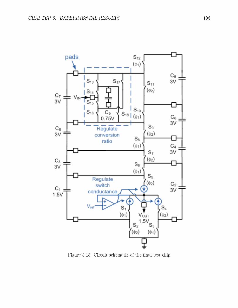
CHAPTER 5. EXPERIMENTAL RESULTS 106
Figure 5.15: Circuit schematic of the nal test chip
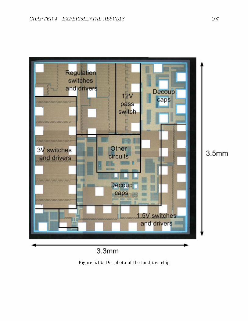
CHAPTER 5. EXPERIMENTAL RESULTS 107
Figure 5.16: Die photo of the nal test chip
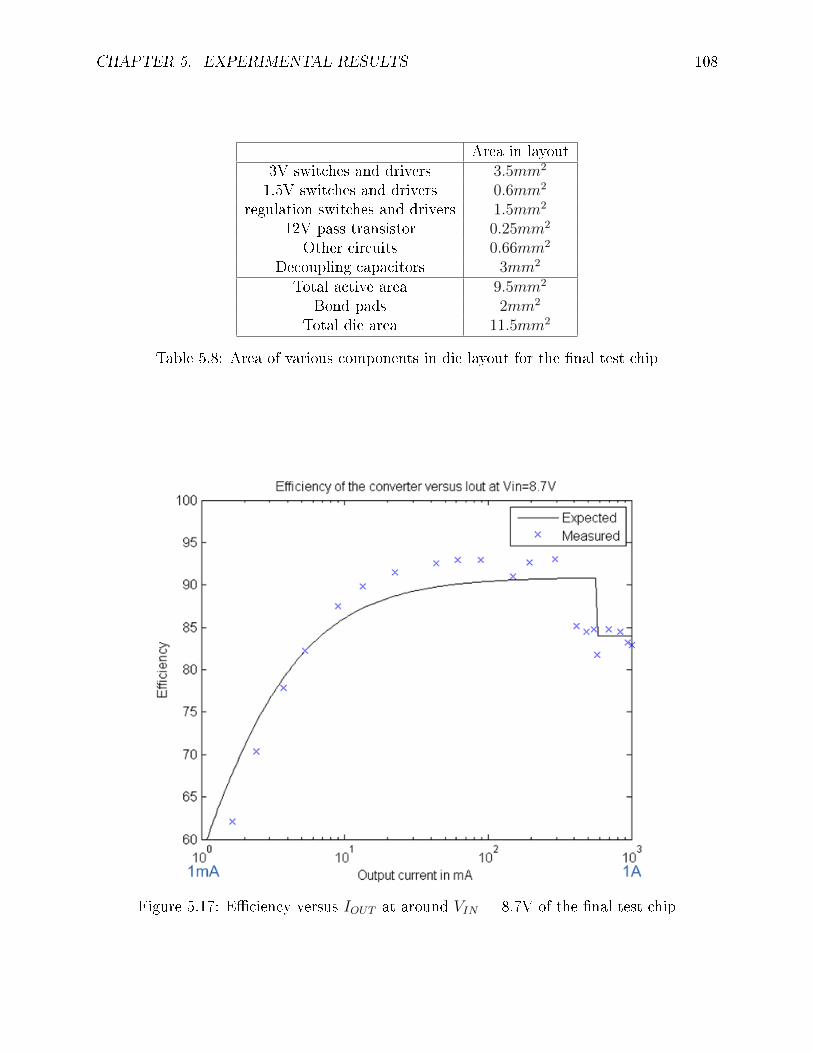
CHAPTER 5. EXPERIMENTAL RESULTS 108
Area in layout3V switches and drivers 3.5mm2
1.5V switches and drivers 0.6mm2
regulation switches and drivers 1.5mm2
12V pass transistor 0.25mm2
Other circuits 0.66mm2
Decoupling capacitors 3mm2
Total active area 9.5mm2
Bond pads 2mm2
Total die area 11.5mm2
Table 5.8: Area of various components in die layout for the nal test chip
Figure 5.17: Eciency versus IOUT at around VIN = 8.7V of the nal test chip
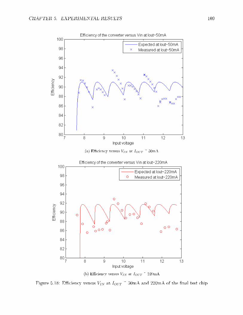
CHAPTER 5. EXPERIMENTAL RESULTS 109
(a) Eciency versus VIN at IOUT ~ 50mA
(b) Eciency versus VIN at IOUT ~ 220mA
Figure 5.18: Eciency versus VIN at IOUT ~ 50mA and 220mA of the nal test chip

CHAPTER 5. EXPERIMENTAL RESULTS 110
(a) Contour plot in color
(b) Contour plot in contour lines
Figure 5.19: Contour plot showing eciency versus VIN and IOUT for the nal test chip.
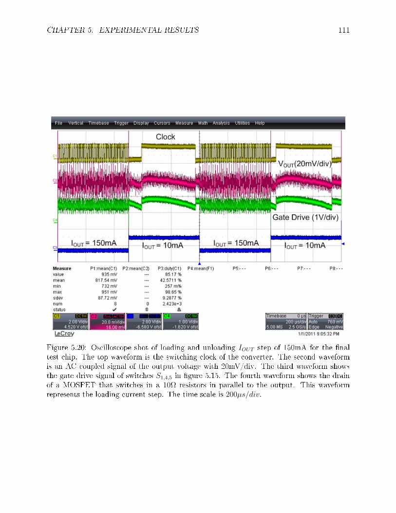
CHAPTER 5. EXPERIMENTAL RESULTS 111
Figure 5.20: Oscilloscope shot of loading and unloading IOUT step of 150mA for the naltest chip. The top waveform is the switching clock of the converter. The second waveformis an AC coupled signal of the output voltage with 20mV/div. The third waveform showsthe gate drive signal of switches S1,4,5 in gure 5.15. The fourth waveform shows the drainof a MOSFET that switches in a 10Ω resistors in parallel to the output. This waveformrepresents the loading current step. The time scale is 200µs/div.
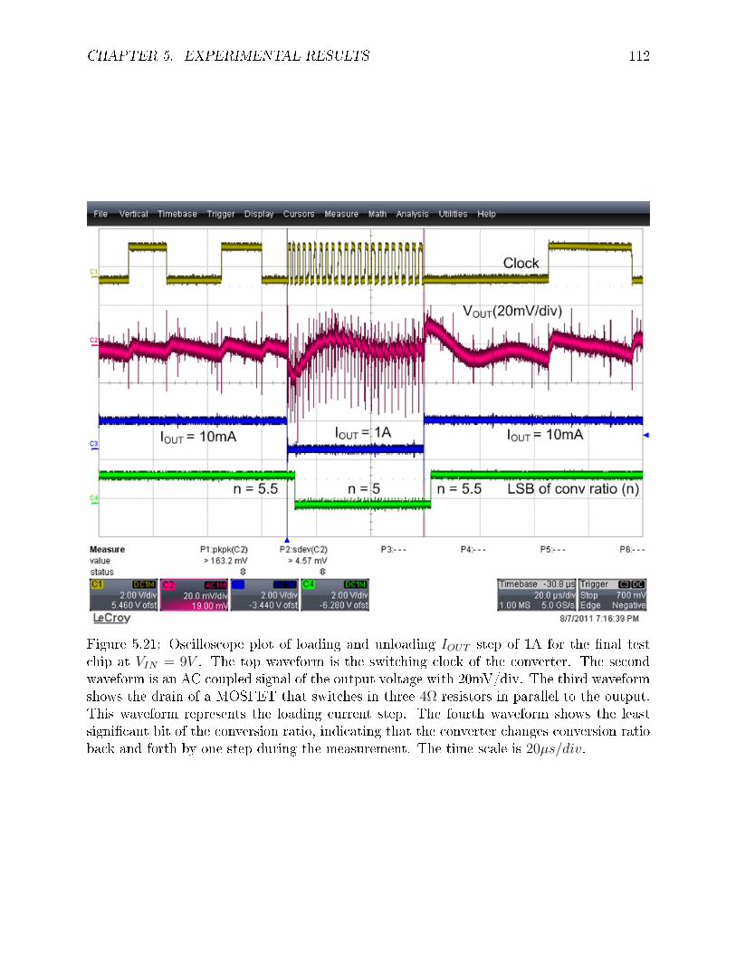
CHAPTER 5. EXPERIMENTAL RESULTS 112
Figure 5.21: Oscilloscope plot of loading and unloading IOUT step of 1A for the nal testchip at VIN = 9V . The top waveform is the switching clock of the converter. The secondwaveform is an AC coupled signal of the output voltage with 20mV/div. The third waveformshows the drain of a MOSFET that switches in three 4Ω resistors in parallel to the output.This waveform represents the loading current step. The fourth waveform shows the leastsignicant bit of the conversion ratio, indicating that the converter changes conversion ratioback and forth by one step during the measurement. The time scale is 20µs/div.
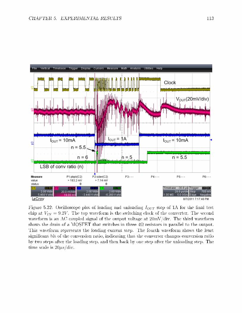
CHAPTER 5. EXPERIMENTAL RESULTS 113
Figure 5.22: Oscilloscope plot of loading and unloading IOUT step of 1A for the nal testchip at VIN = 9.2V . The top waveform is the switching clock of the converter. The secondwaveform is an AC coupled signal of the output voltage at 20mV/div. The third waveformshows the drain of a MOSFET that switches in three 4Ω resistors in parallel to the output.This waveform represents the loading current step. The fourth waveform shows the leastsignicant bit of the conversion ratio, indicating that the converter changes conversion ratioby two steps after the loading step, and then back by one step after the unloading step. Thetime scale is 20µs/div.
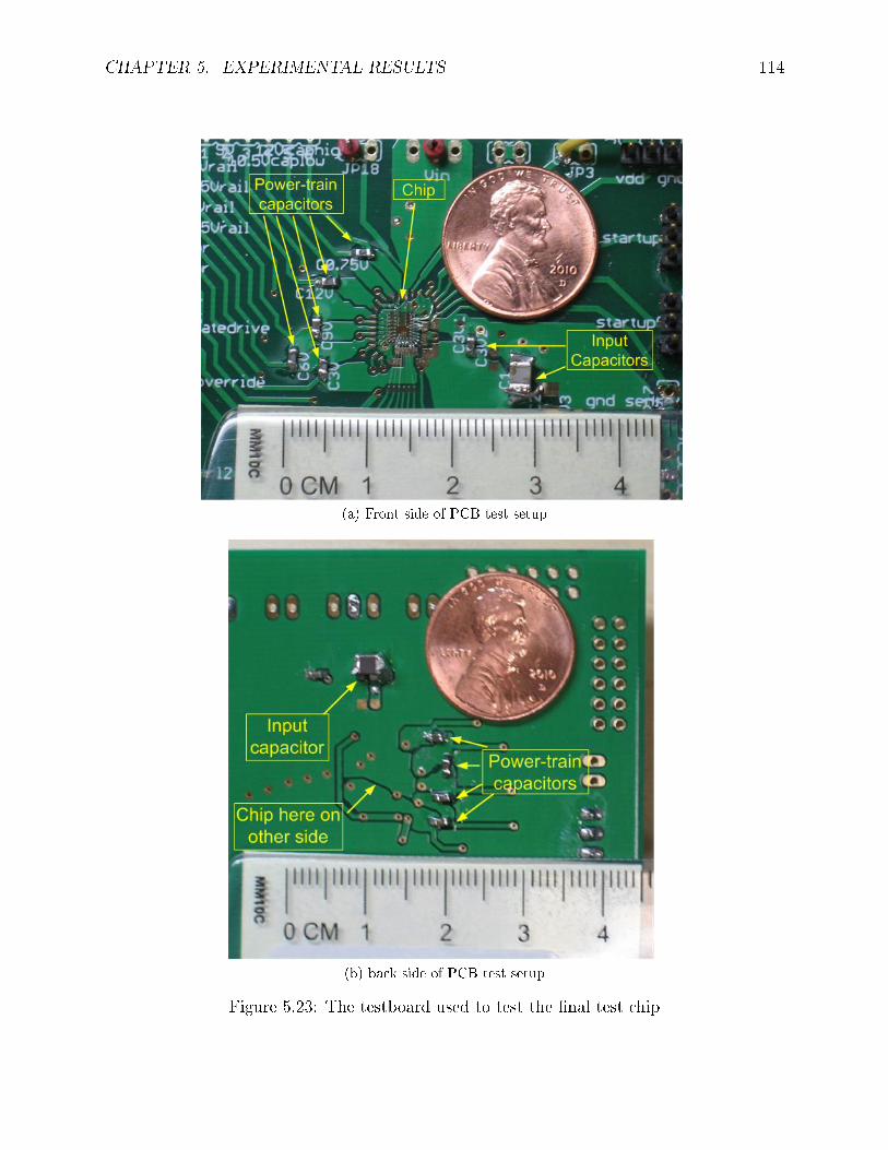
CHAPTER 5. EXPERIMENTAL RESULTS 114
(a) Front side of PCB test setup
(b) back side of PCB test setup
Figure 5.23: The testboard used to test the nal test chip
CHAPTER 5. EXPERIMENTAL RESULTS 115
than the gain-bandwidth product of the overall feedback loop. This requirement can beremoved if switch conductance regulation is eliminated and the inner loop controller onlychanges switching frequency. As discussed in section 3.1, this represents a potential trade-obetween eciency and ripple that the designer can make. Another potential improvementis to use a dierent architecture for the error amplier, for example a class AB outputstage may consume less power. The second largest constant power consumption occurs inthe digital circuits. The error amplier consumes about 375µW of power while the digitalcircuits consumes about 150µW of power, as discussed in chapter 4. The digital circuitsconsume signicant power because they switch at 50MHz, which is signicantly higher thanthe 2.5MHz maximum switching frequency of the converter. While a fast digital controllerallows fast response, there may be limited degradation in regulation performance if thedigital clock runs signicantly slower, and there may be design choices to allow a reductionin switching frequency without compromising performance. All of these design choices areinteresting topics to investigate but were not considered here because of the focus of thisversion of implementation. Thus while this version of implementation shows a reduction ineciency in light load conditions, there is ample room for improvement and the results byno means represent a fundamental limit to the switched capacitor dc-dc converter.
5.5 Comparison with other works
Fig. 5.24 shows a comparison of the peak eciency between the last test chip in this workand other works. All the surveyed buck and SC converters achieve respectable eciency,but shows a general trend of reduced eciency as conversion ratio increases. This trendmirrors the analysis in subsection 1.2.1. This work not only shows a signicant increase ineciency and conversion ratio when compared to surveyed SC converters, but also showsan improvement with respect to surveyed buck converters. Table 5.9 further compares theother important parameters of a dc-dc converter. This work maintains an eciency higherthan 80% over a very wide range of output load current, and wider than any of the sur-veyed converters. This work also obtains a similar or better peak to peak output transientwith comparable input and output capacitance. In terms of passive components, this workachieves an overall reduction in PCB area and passive component cost when compared to dc-dc converters with similar ratings. While this work replaces the single inductor of the buckconverter with 8 capacitors, the additional capacitors are considerably smaller and cheaperthan the single inductor. This allows an overall reduction in aggregate PCB footprint andcost of the passive components. This comparison only considers input/output capacitors,inductors and power-train capacitors because other auxiliary passives required for compen-sation, start-up etc. are not fundamental and are eliminated or minimized in leading moderndesigns. The estimated cost of capacitors or inductors are based on large-volume purchaseper-unit prices from Digikey.
This work demonstrates that SC converters not only can attain higher performance, butat the same time shrink the area and cost of passive components when compared with buckconverters. The topology demonstrates superior performance compared to previous worklargely due to improvements in the architecture, circuit design and device utilization.
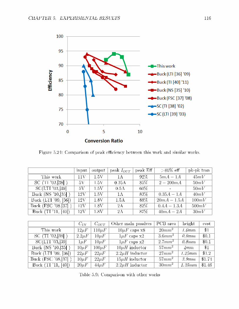
CHAPTER 5. EXPERIMENTAL RESULTS 116
Figure 5.24: Comparison of peak eciency between this work and similar works.
input output peak IOUT peak E >80% e pk-pk tran
This work 11V 1.5V 1A 92% 5mA− 1A 45mVSC (TI '02,[38] ) 5V 1.5V 0.25A 85% 2− 200mA 50mVSC(LTI '03,[39] 5V 1.5V 0.5A 60% - 50mV
Buck (NS '10,[35] ) 12V 1.5V 1A 83% 0.35A− 1A 40mVBuck (LTI '09, [36]) 12V 1.8V 1.5A 88% 20mA− 1.5A 100mVBuck (FSC '08,[37] ) 12V 1.8V 2A 82% 0.4A− 1.3A 500mVBuck (TI '11, [40]) 12V 1.8V 2A 87% 40mA− 2A 30mV
CIN COUT Other main passives PCB area height cost
This work 12µF 110µF 10µF caps x8 20mm2 1.6mm $1SC (TI '02,[38] ) 2.2µF 10µF 1µF caps x2 3.6mm2 0.8mm $0.1SC(LTI '03,[39] 1µF 10µF 1µF caps x2 2.7mm2 0.8mm $0.1
Buck (NS '10,[35] ) 10µF 100µF 10µH inductor 57mm2 4mm $1Buck (LTI '09, [36]) 22µF 22µF 2.2µH inductor 27mm2 1.25mm $1.2Buck (FSC '08,[37] ) 10µF 22µF 15µH inductor 57mm2 3.9mm $1.74Buck (TI '11, [40]) 20µF 44µF 2.2µH inductor 30mm2 1.25mm $1.46
Table 5.9: Comparison with other works
CHAPTER 6. CONCLUSION 117
Chapter 6
Conclusion
The traditional inductor-based buck converter has been the default design for most switched-mode voltage regulators for decades. In its simplest form, the buck converter contains onlytwo switches, one inductor, and the input capacitor[1]. Due to its relatively simple struc-ture and control methodology, it is the dominant design for applications that require tightregulation (<10mV), high eciency (>90%) and high output power (>100mW). Switchedcapacitor (SC) dc-dc converters, on the other hand, have traditionally been used in lowpower (<10mW) and low conversion ratio (<4:1) applications where neither regulation noreciency is critical. This work encompasses the complete successful design, fabrication, andtest of a CMOS based switched capacitor dc-dc converter, addressing the ubiquitous 12V to1.5V board-mounted point-of-load application. In particular, the circuit developed in thiswork attains higher eciency (92% peak, and >80% over a load range of 5mA to 1A) thansurveyed competitive buck converters, while requiring less board area and less costly pas-sive components. The topology and controller enable a wide input range of 7.5V to 13.5V.Controls based on feedback and feedforward provide tight regulation under worst case lineand load step conditions. This work shows that the SC converter can outperform the buckconverter, and thus the scope of SC converter application can and should be expanded.
While this work shows the high potentials of SC converters, it is a only a step in fullyrecognizing the full benet. It will be interesting to investigate the performance of the SCconverters if capacitors that are more integrated are used to replace the discrete ceramiccapacitors in this work. The capacitors can be fully integrated [8], or co-packaged on thedie, or realized with deep-trench capacitors on an accompanying substrate. Using thesecapacitor technologies can further reduce the PCB footprint of dc-dc converters, and allowsmaller sizes in electronic components where small is beautiful.
In terms of expanding the scope of SC converters, it may be interesting to further increasethe output current level or the conversion ratio. It may be interesting to see how multi-phase can aect the operation and whether it provides signicant reduction in the outputcapacitor as in the case of the buck converter [26]. In terms of regulation, there may existsother topologies that can give ner conversion ratio steps while keeping the complexity ofthe circuit at a minimum. With so many capacitors and switches, there may be dierenttechniques for regulation. As discussed in section 3.3, this work simplies the controllerconsiderably, but there may be benets in keeping some of the complexity in order to furtherincrease the performance and eciency of the converter. All of these methods show that

CHAPTER 6. CONCLUSION 118
there are still many work that can be done on the SC converter to even further its potentialadvantage towards the traditional buck converter.
The benets of the SC converter is clear, the only drawback is that it has not been fullyunderstood yet. This work makes a step in understanding the SC converter, and shows thatit has huge potentials. One day it may even dominate the market of dc-dc converters, andit will be the inductor-based buck converter that is limited to specic applications.
BIBLIOGRAPHY 119
Bibliography
[1] J.G. Kassakian, M.F. Schlecht, and G.C. Verghese, Principles of Power Electronics,Addison-Wesley, 1991.
[2] M.S. Makowski and D. Maksimovic, Performance limits of switched-capacitor dc-dcconverters, IEEE Power Electronics Specialists Conference, vol.2, pp. 1215-1221, June1995.
[3] M. Seeman and S. Sanders, Analysis and Optimization of Switched-Capacitor DC-DCConverters, IEEE Trans. on Power Electronics, vol. 23, no. 2, March 2008.
[4] M. Seeman, V. Ng, H.-P. Le et. al, A Comparative Analysis of Switched-Capacitorand Inductor-Based DC-DC Conversion Technologies, IEEE Workshop on Control andModeling of Power Electronics, June 2010
[5] M. Seeman, A Design Methodology for Switched-Capacitor DC-DC Converters, PhDDissertation, UC Berkeley, May 2009.
[6] J.F. Dickson, On-chip high-voltage generation in NMOS integrated circuits using animproved voltage multiplier technique, IEEE J. Solid-State Circuits, vol 11, pp 376-378,June 1976.
[7] D. Wolaver, Fundamental study of DC-DC conversion systems," Ph.D. dissertation,M.I.T., February 1969.
[8] H.-P. Le, M. Seeman, S. Sanders et. al, "A 32nm Fully Integrated RecongurableSwitched-Capacitor DC-DC Converter Delivering 0.55W/mm2 at 81% Eciency",ISSCC Dig. Tech. Papers, pp. 210-211, February 2010.
[9] J. Wibben and R. Harjani, A High-Eciency DCDC Converter Using 2nH IntegratedInductors IEEE J. Solid-States Circuits, vol 43, April 2008.
[10] J. Lee, G. Hatcher, L. Vandenberghe and C.K. Yang, Evaluation of Fully-IntegratedSwitching Regulators for CMOS Process Technologies IEEE Trans on VLSI Systems,vol 15, September 2007.
[11] R. Erickson and D. Maksimovic, Fundamentals of Power Electronics Kluwer AcademicPublishers, 2001.
BIBLIOGRAPHY 120
[12] K.H. Liu and F.C. Lee, Zero-voltage switching technique in DC/DC converters, IEEETrans. on Power Electronics, vol. 5, July 1990.
[13] F. Canales, F, P. Barbosa and F.C. Lee, A zero-voltage and zero-current switchingthree-level DC/DC converter, IEEE Trans. on Power Electronics, vol. 17, November2002.
[14] Werner Muth, Matrix Method for Latch-up Free Demonstration in a Triple-Well Bulk-Silicon Technology, IEEE Trans. on Nuclear Science, vol 9, June 1992.
[15] S. Voldman et. al, Latchup in merged triple well structure Proceedings of reliabilityphysics symposium, April 2005.
[16] P. Gray, P. Hurst, S. Lewis and R. Meyer, Analysis and design of analog integratedcircuits John Wiley & Sons Inc, 2001.
[17] T. Tanzawa and T. Tanaka, A dynamic analysis of the Dickson charge pump circuitIEEE J. Solid-States Circuits, vol 32, August 1997.
[18] J.T. Wu and K.L. Chang, MOS Charge Pumps for Low-Voltage Operation, IEEE J.Solid-State Circuits, vol 33, April 1998.
[19] C.C. Wang and J.C. Wu, Eciency Improvement in Charge Pump Circuits, IEEE J.Solid-State Circuits, vol 32, June 1997.
[20] G. Rincon-Mora and P. Allen, A Low-Voltage, Low Quiescent Current, Low Drop-OutRegulator IEEE J. Solid-State Circuits, vol 33, January 1998
[21] E. Bayer and H. Schmeller, Charge Pump with Active Cycle Regulation - Closing theGap between Linear- and Skip Modes IEEE Power Electronics Specialists Conference,vol 3, pp. 1497-1502, August 2000.
[22] M.D. Seeman, S.R. Sanders and J.M. Rabaey, "An Ultra-Low-Power Power ManagementIC for Wireless Sensor Nodes", IEEE Custom Integrated Circuits Conference, pp. 567-570, September 2007.
[23] B. Gregoire, A Compact Switched-Capacitor Regulated Charge Pump Power SupplyIEEE J. Solid-States Circuits, vol 41, August 2006.
[24] G. Zhu and A. Ioinovici, Switched-Capacitor Power Supplies: DC Voltage Ratio, Ef-ciency, Ripple, Regulation IEEE Symp. Circuits and Systems, vol 1, pp. 553-556,August 2002.
[25] S. Ben-Yaakov and A. Kushnerov, Algebraic Foundation of Self-Adjusting SwitchedCapacitors Converters IEEE Energy Conversion Congress and Expo, pp. 1582-1589,September 2009.
[26] J. Han, A. Jouanne, and G. Temes A New Approach to Reducing Output Ripplein Switched-Capacitor-Based Step-Down DCDC Converters IEEE Trans. on PowerElectronics, vol. 21, November 2006.
BIBLIOGRAPHY 121
[27] G. Eirea, and S. Sanders, Adaptive Output Current Feedforward Control in VR Ap-plications IEEE Power Electronics Specialists Conference, June 2007
[28] S. Rajapandian, K. Shepard, P. Hazucha and T. Karnik, High-Voltage Power DeliveryThrough Charge Recycling IEEE J. Solid-States Circuits, vol 41, June 2006.
[29] J. Rabaey, A. Chandrakasan and B. Nikolic, Digital Integrated Circuits: A DesignPerspective Prentice Hall Electronics and VLSI series, 2003
[30] B. Razavi, Design of Analog CMOS Integrated Circuits McGraw-Hill Series in Elec-trical and Computer Engineering, 2001
[31] M. Seeman, S. Sanders and J. Rabaey, "An Ultra-Low-Power Power Management ICfor Wireless Sensor Nodes", IEEE Custom Integrated Circuits Conference, Sept 2007
[32] V. Ng and S. Sanders, "A 98% Peak Eciency 1.5A 12V-to-1.5V Switched CapacitorDC-DC Converter in 0.18um CMOS Technology", Master's Thesis, EECS Department,University of California, Berkeley, Jan 2008.
[33] V. Ng, M. Seeman, S. Sanders, "High-Eciency, 12V-to-1.5V DC-DC Converter Real-ized with Switched Capacitor Architecture", IEEE Symposium on VLSI Circuits, June2009
[34] V. Ng, M. Seeman, S. Sanders, "Minimum PCB Footprint Point-of-Load DC-DCConverter Realized with Switched Capacitor Architecture", IEEE Energy ConversionCongress and Exposition, Sept 2009
[35] National Semiconductor Inc (LMZ12001), 1A SIMPLE SWITCHER Power Modulewith 20V Maximum Input Voltage, June 2010
[36] Linear Technology (LTC3601), 1.5A, 15V Monolithic Synchronous Step-Down Regula-tor, 2009.
[37] Fairchild Semiconductor Inc (FAN8301), 2A, 16V, Non-synchronous Step-down,DC/DC Regulator, November 2008.
[38] Texas Instruments (TPS60503), High Eciency, 250mA step-down charge pump, Feb2002.
[39] Linear Technology (LTC3251), 500mA High Eciency, Low Noise, Inductorless Step-Down DC/DC Converter, 2003
[40] Texas Instruments (TPS54226), 4.5V to 18V Input, 2-A Synchronous Step-DownSWIFT Converter with Eco-Mode, Feb 2011.
[41] L. Salem, and R. Jain, A Novel Switched-Capacitor DC-DC Converter Ripple Mitiga-tion Technique, IEEE International Symposium on Circuits and Systems, June 2010

122
Appendix
Below is the verilog code used to generate the digital controller in this work.
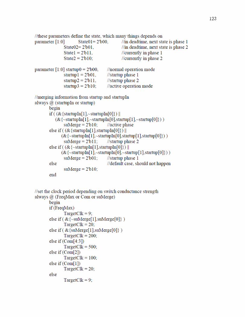
123

124
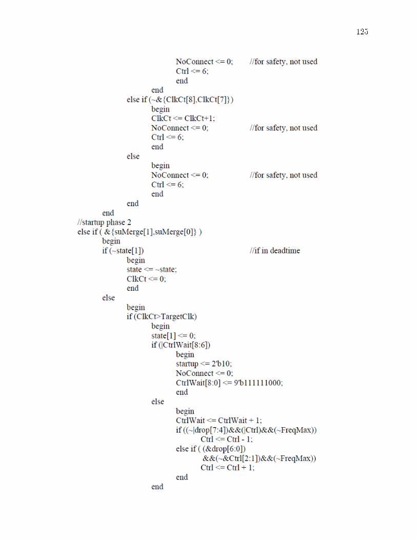
125

126
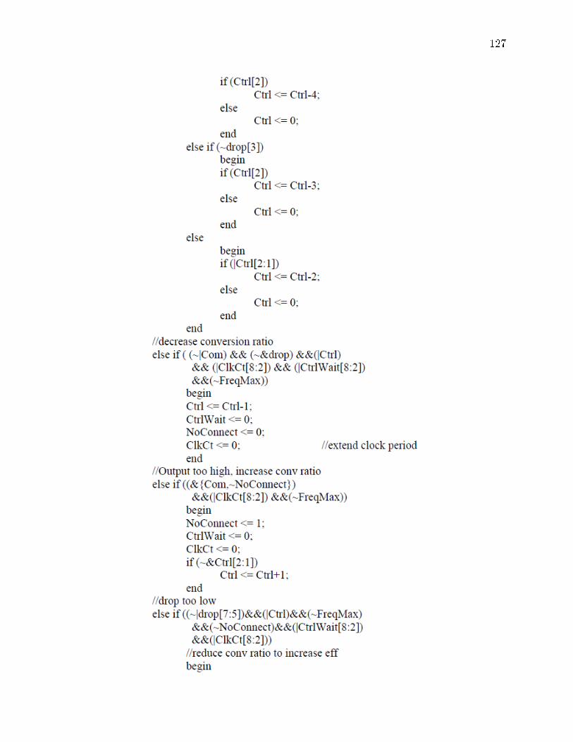
127

128


![Control Method of Flying Capacitor Converter Operated in ...itohserver01.nagaokaut.ac.jp/itohlab/paper/2018/... · density of a DC-DC converter [13]. The proposed control operates](https://img.pdfslide.us/doc/110x75/5e78cf267602f0107d092983/control-method-of-flying-capacitor-converter-operated-in-density-of-a-dc-dc.jpg)