Embed Size (px)
Citation preview

POLITECNICO DI MILANO
Scuola di Ingegneria Industriale e dell’Informazione
Corso di Laurea Magistrale in Ingegneria Elettrica
An Integrated Control Scheme For Dynamic Voltage Restorer
To
Limit Downstream Fault Currents
Author: Ali Bahrami Matricola: 823535
Supervisor: Prof. Roberto Faranda
Academic Year 2016-2017
An Integrated Control Scheme For Dynamic Voltage Restorer
To
Limit Downstream Fault Currents
By
Ali Bahrami
Politecnico di Milano, Italy
Energy Department September, 2017


Preface
This thesis is accomplished as a completion of the master education in Politecnico di Milano. The project has been followed by the main supervisor professor Roberto Faranda and under advisement of PhD. Hossein Hafezi at the Energy Department of Politecnico di Milano.
The project is entitled “An integrated control scheme for dynamic voltage restorer to limit downstream fault currents” where the aim of the project is:
Design and control of a dual functional dynamic voltage restorer inserted into a specified LV-distribution system with the emphasis put on the fault current limiting function. This research project is encouraged by a desire of acquiring knowledge about power quality, voltage dip mitigation, modelling and simulation of components in the distribution system, analysis of Custom Power Systems (CUPS) and comprehensive investigation of dynamic voltage restorer (DVR) in order to employ a fault current limiting technique to protect both network and DVR at the moment of fault occurrence. The dynamic voltage restorer could be a solution which is offered by DSOs to customers, who are willing to pay for a high quality voltage.
Several persons have contributed academically, practically and with support to this master thesis, therefore I would like to thank all of them. In particular I am grateful to my head supervisor Roberto Faranda and co-supervisors Hossein Hafezi for their time, valuable guidance and support throughout the entire project period.
Ali Bahrami Milan, September 2017
Abstract
This thesis is the main results from a MSc project under the research plan at Politecnico di Milano. The main topic in the thesis is design an integrated control scheme for a dynamic voltage restorer (DVR) to limit downstream fault currents. During the thesis knowledge is gathered about power and voltage quality issues, power electronic solutions for voltage quality improvement, design and control of a DVR either connected at the low voltage or the medium voltage level. In addition researches are performed in order to find out a reliable and economically justified strategy of the fault current limiting function in order to integrate with a DVR.
DVR is a custom power system device with the principal duty to protect sensitive electric consumers against voltage dips and surges in the medium and low voltage distribution which is series connected in the grid. Voltage dips can in many cases be the most considerable power quality problem, because they can occur very frequently and lead to a load tripping. Voltage dip depth, duration and phase jump depend on the location of the fault and the protection equipment used. The thesis first presents an introduction to relevant power quality issues, thereafter possible solutions and strategies including employing a DVR in order to compensate the voltage quality problems are investigated. Consequently the operation principle and the elements in a DVR are described. The advantages and disadvantages of inserting a DVR in the distribution system (either the medium voltage or low voltage) are discussed. Then different topologies and configurations of the VSC are investigated. The four DVR topologies, which are presented and compared, are:
Topologies with stored energy devices: – Constant DC-link voltage; – Variable DC-link voltage;
Topologies with power from the supply: – Supply side connected shunt converter; – Load side connected shunt converter;
Different proposed compensation methods in the literatures to employ a DVR, including “pre-sag compensation method, the method by which the phases of the load voltages are unchanged”, “in-phase compensation method, the method by which the injected voltage is in-phase with supply voltage” and “energy optimal compensation method, the method by which the injected voltage is perpendicular to the load current” are reviewed. Consequently a comparison between these scenarios is treated and their pros and cons are expressed. Also the control concepts of the DVR are described. Then the control system in 3-phase applications is implemented in a rotating dq-reference frame, which gives a very good compensation of the positive sequence component and a damping of the negative sequence. Zero sequence components are not detected or compensated with the chosen control method.
A set of simulations in Matlab environment for normal operation conditions and voltage dip occurrence have been carried out. The results indicate that the DVR can compensate voltage dips for different kind of loads, however non-linear loads can lead to oscillations in the line-filter of the DVR and thereby an increased harmonic distortion of the load voltages. The dynamic simulations with the LV-DVR indicate an acceptable compensation of symmetrical voltage dips. In most cases the DVR is capable of restoring the load voltages within a very short time. During the transition phases load voltage oscillations can be generated and during the return of the supply voltages short time over-voltages can be generated by the DVR. Both of the described events can be a potential problem for sensitive loads.
Unfortunately faults do occur on the distribution system downstream of the DVR. Faulted point could be anywhere on the feeder connecting the DVR and the protected load, considering the fact that DVR is series connected to the faulted feeder, a large current will pass through the injection transformer and into the DVR converter. Without proper considerations, the high short circuit current could easily damage the injection transformer, destroy insulators and more important break power electronic switches which are more sensitive to high current. In order to isolate the downstream fault, one can of course rely on the circuit breakers installed upstream of the DVR. Depending on algorithm of protection coordination and the exact location/nature of the fault, the fault clearing action may typically take some cycles. However, fault current during these cycles can have damaging effect on the power switching devices within the DVR. Moreover, for other loads connected to parallel feeders, the voltage sag event due to fault current can be harmful as it can cause equipment on these feeders to fail, malfunction, or shut down.
Voltage sag on the three-phase system is not uniformly distributed on different phases and oftentimes there is significant accumulation of voltage sags on one phase. Also taking into account that some electrical consumers are more sensitive with respect to voltage disturbance rather than other consumers, DSOs would be interested in installing series voltage compensator only at single-phase configuration. Therefore during the chapter three the emphasis is put on implementing the fault current limiting function for a single-phase DVR. However the obtained results are capable to be extended to three-phase applications without the loss of generality.
In order to limit fault currents through a DVR some strategies are presented in literatures. During the chapter three the operation principle of the most presented strategies in order to limit the short circuit current are investigated. The key idea of these solutions is to effectively insert series impedance between the source and the fault location. It should be highlighted that the duty of the DVR under such a downstream fault condition is to limit the fault current until such time when the protection system upstream of the DVR operates. Therefore we may say that the DVR is not supposed to replace the protection system, it only provides a short-term action to limit the fault current.
A comprehensive fault analysis and computer simulations were done on a defined LV-distribution systems. Then the short circuit current waveform and its transient behavior are considered. The fault detection/recovery methods are investigated. Thereafter different configurations in order to limit the fault current including active and passive strategies, their feasibility and reliability together with economic considerations are discussed. Active solutions are applicable in impedance mode and reactance mode. Presence of communication channel is an important requirement in order to use active FCL strategies. The treated strategies in the literatures in order to implement the FCL function for a DVR through passive elements including “Using the impedance of the injection transformer” and “Using the filter reactance” are analyzed and simulated.
Thereafter a new configuration in order to limit the short circuit current is proposed. This configuration is based on taking the benefits of both bypassing the DVR during the faulted condition and implementing DVR FCL function. At the end a comparison between the effectiveness of different strategies is expressed too.
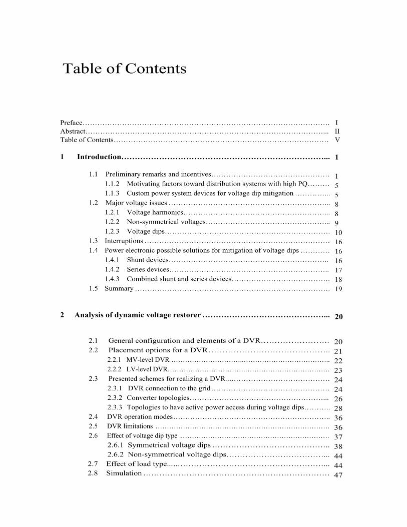
Table of Contents
Preface……………………………………………………………………………………….Abstract……………………………………………………………………………………...Table of Contents……………………………………………………………………………
1 Introduction…………………………………………………………………...
1.1 Preliminary remarks and incentives…………………………………………
1.1.2 Motivating factors toward distribution systems with high PQ………1.1.3 Custom power system devices for voltage dip mitigation …………...
1.2 Major voltage issues ………………………………………………………...1.2.1 Voltage harmonics…………………………………………………...1.2.2 Non-symmetrical voltages…………………………………………...
1.2.3 Voltage dips………………………………………………………….1.3 Interruptions …………………………………………………………………1.4 Power electronic possible solutions for mitigation of voltage dips …………
1.4.1 Shunt devices………………………………………………………..
1.4.2 Series devices………………………………………………………..1.4.3 Combined shunt and series devices………………………………….
1.5 Summary …………………………………………………………………….
2 Analysis of dynamic voltage restorer ………………………………………...
2.1 General configuration and elements of a DVR…………………….2.2 Placement options for a DVR ……………………………………..
2.2.1 MV-level DVR …………………………..………………………………..2.2.2 LV-level DVR…………………………….……………………………….
2.3 Presented schemes for realizing a DVR ....…………………………………
2.3.1 DVR connection to the grid …………………………………………2.3.2 Converter topologies………………………………………………...2.3.3 Topologies to have active power access during voltage dips………..
2.4 DVR operation modes ………………………………………………………..2.5 DVR limitations ………………………………………………………………….2.6 Effect of voltage dip type ..……………………………………………………….
2.6.1 Symmetrical voltage dips ……………………………………..2.6.2 Non-symmetrical voltage dips………………………………...
2.7 Effect of load type... ..………………………………………………...2.8 Simulation ……………………………………………………………
I II V 1 1 5 5 8 8 9 10 16 16 16 17 18 19
20
20 21 22 23 24 24 26 28 36 36 37 38 44 44 47
2.9 Summary……………………………………………………………….
3 Implementing fault current limiting function ………………………………..
3.1 Incentives ……………………………………………………………………...3.2 Network fault analysis…………………………………………………………
3.2.1 Necessity of fault analysis .…………………………………………...3.2.2 Short circuit current waveform……………………………………….3.2.3 Fault effects…………………………………………………………...3.2.4 Short circuit current terminology and definitions…………………….
3.3 Single-phase DVR applications .………………………………………………3.4 Fault/Recovery detection techniques ………………………………………….3.5 Bypassing the DVR ……………………………………………………………3.6 Active fault current limiting (FCL) function implementation ………………...
3.6.1 Active impedance FCL strategy ………………………………………3.6.2 Active reactance FCL strategy ………………………………………..
3.7 FCL function implementation through passive elements …………………………3.7.1 Using the impedance of the injection transformer ………………………..3.7.2 Using the filter reactance………………………………………………….3.7.3 Merging the FCL function with the bypass strategy ……………………...
3.8 Comparison of the proposed FCL solutions……………………………………….3.9 Other FCL solutions………………………………………………………………..
3.9.1 Resonant filters...…………………………………………………………...3.9.2 Future work with the superconducting FCL strategy.……………………...
3.10 Summary ..………………………………………………………………………… Conclusions ..………………………………………………………………………………. Appendix ……………………………………………………………………………...
A.1 DVR design parameters………………………………………………………. A.1.1 Voltage, current and energy rating ……………………………………..
A.2 Sizing DVR components……………………………………………………… A.2.1 Converter design………………………………………………………..A.2.2 Series injection transformer design…………………………………….
A.2.3 Filter design ……………………………………………………………A.3 Designing control system of DVR….………………………………...
A.3.1 DVR load voltage controller……………………………………A.3.2 DVR DC-link voltage controller ……………………………….A.3.3 DVR voltage dip detector………………………………………A.3.4 DVR LCL filter response ………………………………………
References………………………………………………………………………………….
49 50 50 51 51 51 52 53 55 61 62 65 67 76 82 83 85 88 91 92 92 93 95 97 98 98 98 101 101 102 104 106 106 112 113 116 118
1
CHAPTER 1
Introduction
1.1 Preliminary remarks and incentives During last decades and together with the development of electrical energy transmission and distribution networks and by increasing the number of grid connected systems including industrial electric power consumers and also less reliable grid connected renewable energy as it is shown in Fig. 1.1, power quality has become a topic of great interest, therefore several measures in order to monitor and improve the quality of power have been investigated.
Figure 1.1 Development of the power system
2
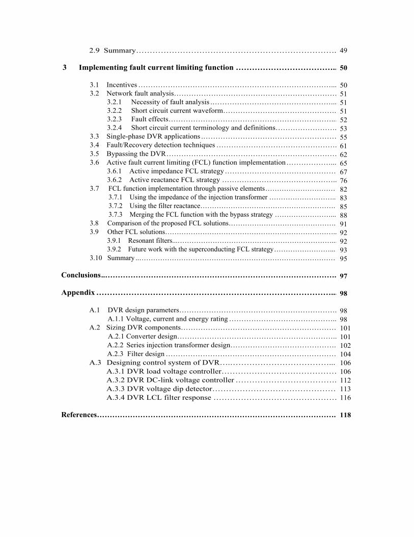
Power quality Today power quality is a service and many customers are paying for it, but in a simple way (in particular for continuity of service). In the future, distribution system operators could decide, or could be obliged by authorities, to supply their customers with different PQ levels and at different prices. In order to evaluate the quality of power in an area and consider the appropriate measures to counteract the poor PQ generally a PQ survey is supposed to be carried out. One of the indicators to analyze the survey data is CBEMA curve. The CBEMA curve1 is a susceptibility profile with the horizontal axis representing the duration of the event, while the vertical axis indicates the percent of voltage applied to the power circuit. In the center of the plot is the so called acceptable area. Voltage values above the envelope are supposed to cause malfunctions such as insulation failure, over-excitation and overvoltage trip. While voltages below the envelope are assumed to cause the load to
Figure 1.2: The curve indicates a voltage tolerance envelope for single-phase 120V equipment. Also it illustrates acceptable area. It is referred as the CBEMA/ITIC curve.
1 CBEMA Curve illustrated in Fig. 1.2 is one of the most frequently employed power acceptability curve. It was developed by the Computer Business Equipment Manufacturers Association in the 1970s, as a guideline for the organization's members in designing their power supplies. Basically, the CBEMA curve was originally derived to describe the tolerance of mainframe computer business equipment to the magnitude and duration of voltage variations on the power system. Also, the association designed the curve to point out ways in which system reliability could be provided for electronic equipment. Eventually, it became a standard design target for sensitive equipment to be applied on the power system and a common format for reporting power quality variation data. The CBEMA curve was adapted from IEEE Standard 446 (Recommended Practice for Emergency and Standby Power Systems for Industrial and Commercial Applications - Orange Book), which is typically used in the analysis of power quality monitoring results. The CBEMA curve was derived from experimental and historical data taken from mainframe computers. The best scientific interpretation of the curve can be given in terms of a voltage standard applied to the DC bus voltage of a rectifier load.
3
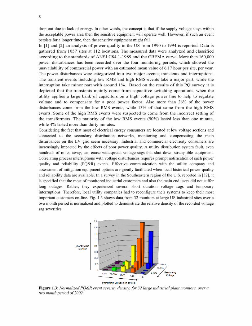
drop out due to lack of energy. In other words, the concept is that if the supply voltage stays within the acceptable power area then the sensitive equipment will operate well. However, if such an event persists for a longer time, then the sensitive equipment might fail. In [1] and [2] an analysis of power quality in the US from 1990 to 1994 is reported. Data is gathered from 1057 sites at 112 locations. The measured data were analyzed and classified according to the standards of ANSI C84.1-1989 and the CBEMA curve. More than 160,000 power disturbances has been recorded over the four monitoring periods, which showed the unavailability of commercial power with an estimated mean value of 6.17 hour per site, per year. The power disturbances were categorized into two major events; transients and interruptions. The transient events including low RMS and high RMS events take a major part, while the interruption take minor part with around 1%. Based on the results of this PQ survey it is depicted that the transients mainly come from capacitive switching operations, when the utility applies a large bank of capacitors on a high voltage power line to help to regulate voltage and to compensate for a poor power factor. Also more than 26% of the power disturbances come from the low RMS events, while 13% of that came from the high RMS events. Some of the high RMS events were suspected to come from the incorrect setting of the transformers. The majority of the low RMS events (90%) lasted less than one minute, while 4% lasted more than thirty minutes. Considering the fact that most of electrical energy consumers are located at low voltage sections and connected to the secondary distribution networks, monitoring and compensating the main disturbances on the LV grid seem necessary. Industrial and commercial electricity consumers are increasingly impacted by the effects of poor power quality. A utility distribution system fault, even hundreds of miles away, can cause widespread voltage sags that shut down susceptible equipment. Correlating process interruptions with voltage disturbances requires prompt notification of such power quality and reliability (PQ&R) events. Effective communication with the utility company and assessment of mitigation equipment options are greatly facilitated when local historical power quality and reliability data are available. In a survey in the Southeastern region of the U.S. reported in [32], it is specified that the most of monitored industrial customers and also the main end users did not suffer long outages. Rather, they experienced several short duration voltage sags and temporary interruptions. Therefore, local utility companies had to reconfigure their systems to keep their most important customers on-line. Fig. 1.3 shows data from 32 monitors at large US industrial sites over a two month period is normalized and plotted to demonstrate the relative density of the recorded voltage sag severities.
Figure 1.3: Normalized PQ&R event severity density, for 32 large industrial plant monitors, over a two month period of 2002.
4
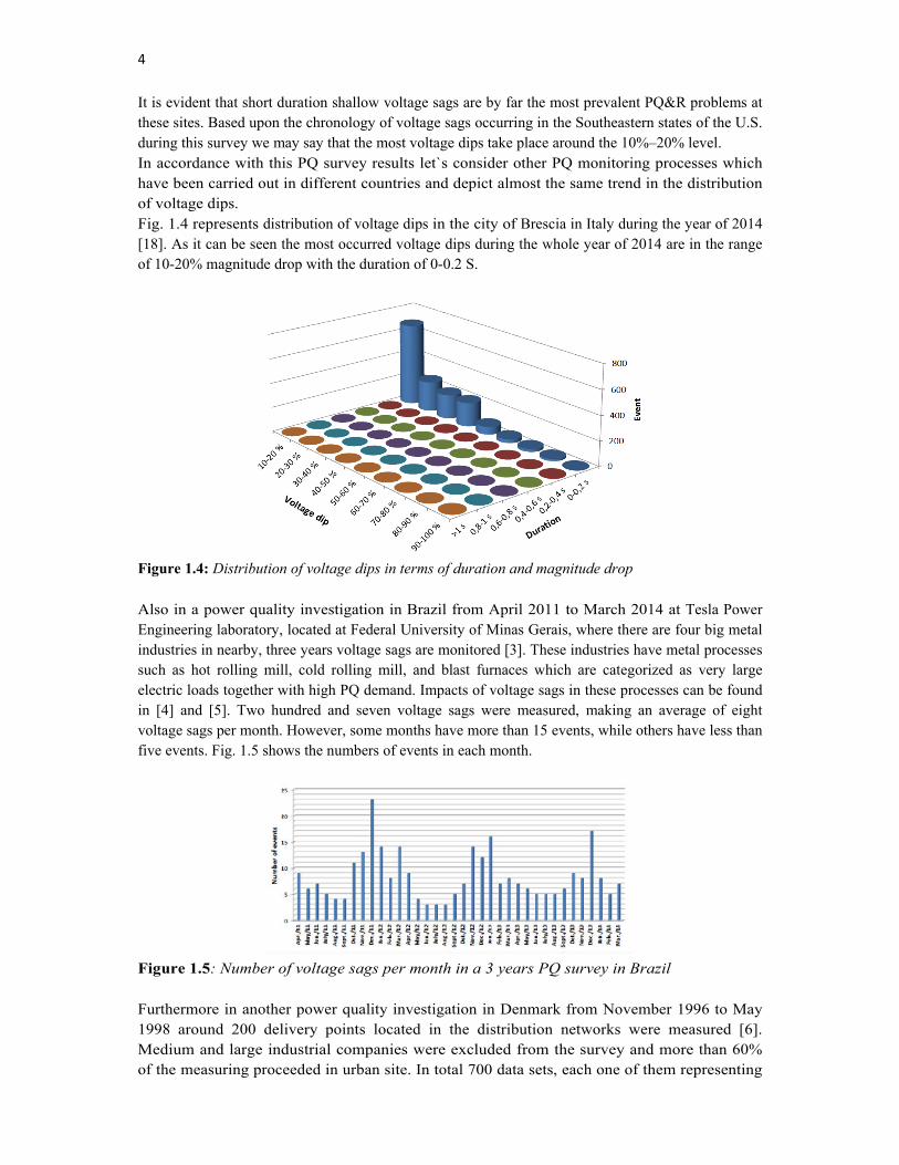
It is evident that short duration shallow voltage sags are by far the most prevalent PQ&R problems at these sites. Based upon the chronology of voltage sags occurring in the Southeastern states of the U.S. during this survey we may say that the most voltage dips take place around the 10%–20% level. In accordance with this PQ survey results let`s consider other PQ monitoring processes which have been carried out in different countries and depict almost the same trend in the distribution of voltage dips. Fig. 1.4 represents distribution of voltage dips in the city of Brescia in Italy during the year of 2014 [18]. As it can be seen the most occurred voltage dips during the whole year of 2014 are in the range of 10-20% magnitude drop with the duration of 0-0.2 S.
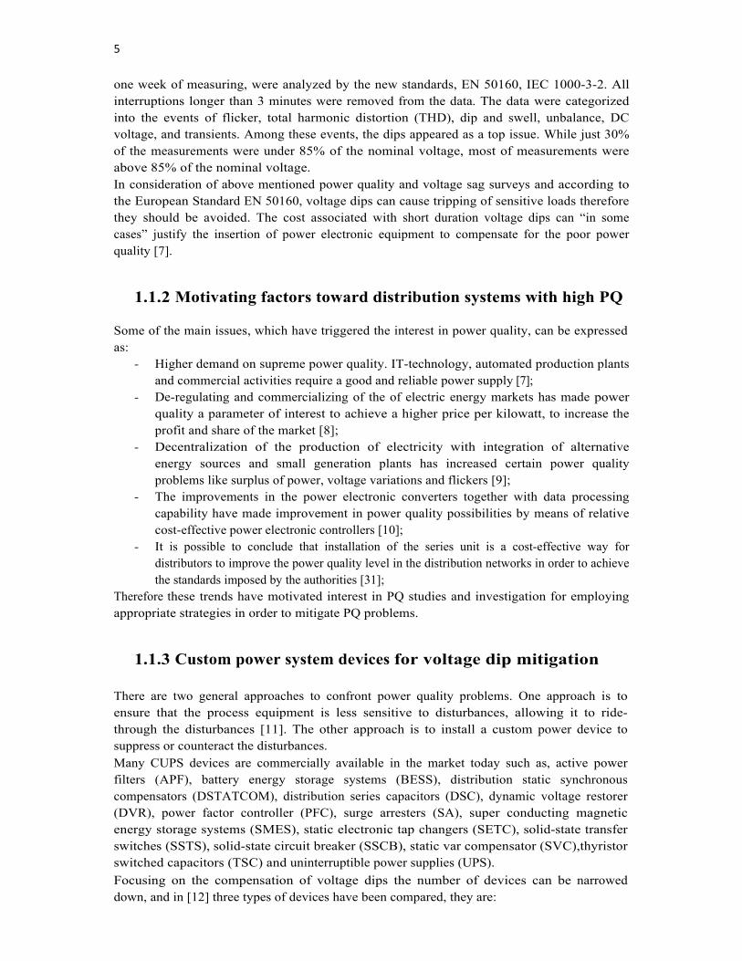
Figure 1.4: Distribution of voltage dips in terms of duration and magnitude drop Also in a power quality investigation in Brazil from April 2011 to March 2014 at Tesla Power Engineering laboratory, located at Federal University of Minas Gerais, where there are four big metal industries in nearby, three years voltage sags are monitored [3]. These industries have metal processes such as hot rolling mill, cold rolling mill, and blast furnaces which are categorized as very large electric loads together with high PQ demand. Impacts of voltage sags in these processes can be found in [4] and [5]. Two hundred and seven voltage sags were measured, making an average of eight voltage sags per month. However, some months have more than 15 events, while others have less than five events. Fig. 1.5 shows the numbers of events in each month.
Figure 1.5: Number of voltage sags per month in a 3 years PQ survey in Brazil Furthermore in another power quality investigation in Denmark from November 1996 to May 1998 around 200 delivery points located in the distribution networks were measured [6]. Medium and large industrial companies were excluded from the survey and more than 60% of the measuring proceeded in urban site. In total 700 data sets, each one of them representing
5
one week of measuring, were analyzed by the new standards, EN 50160, IEC 1000-3-2. All interruptions longer than 3 minutes were removed from the data. The data were categorized into the events of flicker, total harmonic distortion (THD), dip and swell, unbalance, DC voltage, and transients. Among these events, the dips appeared as a top issue. While just 30% of the measurements were under 85% of the nominal voltage, most of measurements were above 85% of the nominal voltage. In consideration of above mentioned power quality and voltage sag surveys and according to the European Standard EN 50160, voltage dips can cause tripping of sensitive loads therefore they should be avoided. The cost associated with short duration voltage dips can “in some cases” justify the insertion of power electronic equipment to compensate for the poor power quality [7].
1.1.2 Motivating factors toward distribution systems with high PQ
Some of the main issues, which have triggered the interest in power quality, can be expressed as:
- Higher demand on supreme power quality. IT-technology, automated production plants and commercial activities require a good and reliable power supply [7];
- De-regulating and commercializing of the of electric energy markets has made power quality a parameter of interest to achieve a higher price per kilowatt, to increase the profit and share of the market [8];
- Decentralization of the production of electricity with integration of alternative energy sources and small generation plants has increased certain power quality problems like surplus of power, voltage variations and flickers [9];
- The improvements in the power electronic converters together with data processing capability have made improvement in power quality possibilities by means of relative cost-effective power electronic controllers [10];
- It is possible to conclude that installation of the series unit is a cost-effective way for distributors to improve the power quality level in the distribution networks in order to achieve the standards imposed by the authorities [31];
Therefore these trends have motivated interest in PQ studies and investigation for employing appropriate strategies in order to mitigate PQ problems.
1.1.3 Custom power system devices for voltage dip mitigation
There are two general approaches to confront power quality problems. One approach is to ensure that the process equipment is less sensitive to disturbances, allowing it to ride-through the disturbances [11]. The other approach is to install a custom power device to suppress or counteract the disturbances. Many CUPS devices are commercially available in the market today such as, active power filters (APF), battery energy storage systems (BESS), distribution static synchronous compensators (DSTATCOM), distribution series capacitors (DSC), dynamic voltage restorer (DVR), power factor controller (PFC), surge arresters (SA), super conducting magnetic energy storage systems (SMES), static electronic tap changers (SETC), solid-state transfer switches (SSTS), solid-state circuit breaker (SSCB), static var compensator (SVC),thyristor switched capacitors (TSC) and uninterruptible power supplies (UPS).
Focusing on the compensation of voltage dips the number of devices can be narrowed down, and in [12] three types of devices have been compared, they are:
6
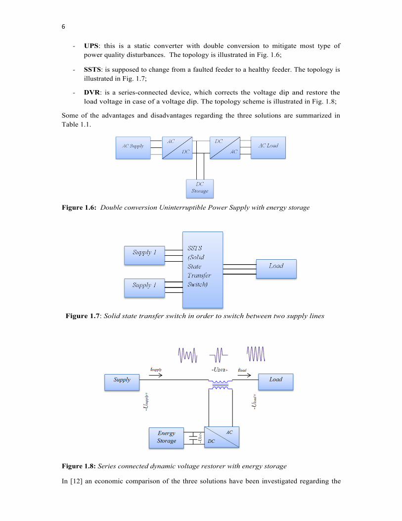
- UPS: this is a static converter with double conversion to mitigate most type of power quality disturbances. The topology is illustrated in Fig. 1.6;
- SSTS: is supposed to change from a faulted feeder to a healthy feeder. The topology is illustrated in Fig. 1.7;
- DVR: is a series-connected device, which corrects the voltage dip and restore the load voltage in case of a voltage dip. The topology scheme is illustrated in Fig. 1.8;
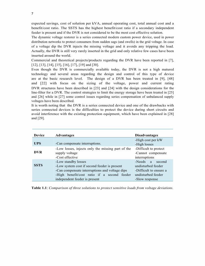
Some of the advantages and disadvantages regarding the three solutions are summarized in Table 1.1.
Figure 1.6: Double conversion Uninterruptible Power Supply with energy storage
Figure 1.7: Solid state transfer switch in order to switch between two supply lines
Figure 1.8: Series connected dynamic voltage restorer with energy storage
In [12] an economic comparison of the three solutions have been investigated regarding the
7
expected savings, cost of solution per kVA, annual operating cost, total annual cost and a benefit/cost ratio. The SSTS has the highest benefit/cost ratio if a secondary independent feeder is present and if the DVR is not considered to be the most cost effective solution. The dynamic voltage restorer is a series connected modern custom power device, used in power distribution networks to protect consumers from sudden sags (and swells) in the grid voltage. In case of a voltage dip the DVR injects the missing voltage and it avoids any tripping the load. Actually, the DVR is still very rarely inserted in the grid and only relative few cases have been inserted around the world. Commercial and theoretical projects/products regarding the DVR have been reported in [7], [12], [13], [14], [15], [16], [17], [19] and [30]. Even though the DVR is commercially available today, the DVR is not a high matured technology and several areas regarding the design and control of this type of device are at the basic research level. The design of a DVR has been treated in [9], [48] and [22] with focus on the sizing of the voltage, power and current rating
DVR structures have been described in [23] and [24] with the design considerations for the line-filter for a DVR. The control strategies to limit the energy storage have been treated in [25] and [26] while in [27] some control issues regarding series compensation of unbalanced supply voltages have been described. It is worth noting that the DVR is a series connected device and one of the drawbacks with series connected devices is the difficulties to protect the device during short circuits and avoid interference with the existing protection equipment, which have been explained in [28] and [29].
Device Advantages Disadvantages
UPS -Can compensate interruptions. -High cost per kW -High losses
DVR -Low losses, injects only the missing part of the supply voltage -Cost effective
-Difficult to protect -Cannot compensate interruptions
SSTS -Low standby losses -Low system cost if second feeder is present -Can compensate interruptions and voltage dips -High benefit/cost ratio if a second feeder independent feeder is present
-Needs a second undisturbed feeder -Difficult to ensure a undisturbed feeder -Slow response
Table 1.1: Comparison of three solutions to protect sensitive loads from voltage deviations.
8
1.2 Major voltage issues
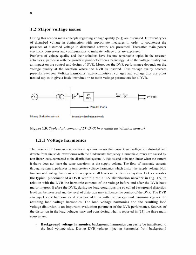
During this section main concepts regarding voltage quality (VQ) are discussed. Different types of disturbed voltage in conjunction with appropriate measures in order to counteract the presence of disturbed voltage in distributed network are presented. Thereafter main power electronic converters and configurations to mitigate voltage dips are expressed. Problems of voltage quality and their solutions have become remarkable topics in the research activities in particular with the growth in power electronics technology. Also the voltage quality has an impact on the control and design of DVR. Moreover the DVR performance depends on the voltage quality at the location where the DVR is inserted. Thus voltage quality deserves particular attention. Voltage harmonics, non-symmetrical voltages and voltage dips are other treated topics to give a basic introduction to main voltage parameters for a DVR.
Figure 1.9: Typical placement of LV-DVR in a radial distribution network
1.2.1 Voltage harmonics
The presence of harmonics in electrical systems means that current and voltage are distorted and
deviate from sinusoidal waveforms with the fundamental frequency. Harmonic currents are caused by
non-linear loads connected to the distribution system. A load is said to be non-linear when the current
it draws does not have the same waveform as the supply voltage. The flow of harmonic currents
through system impedances in turn creates voltage harmonics which distort the supply voltage. Non
fundamental voltage harmonics often appear at all levels in the electrical system. Let`s consider
the typical placement of a DVR within a radial LV distribution network in Fig. 1.9, in
relation with the DVR the harmonic contents of the voltage before and after the DVR have
major interest. Before the DVR, during no-load conditions the so called background distortion
level can be measured and the level of distortion may influence the control of the DVR. The DVR
can inject some harmonics and a vector addition with the background harmonics gives the
resulting load voltage harmonics. The load voltage harmonics and the resulting load
voltage distortion is an important evaluation parameter of the DVR performance. Sources of
the distortion in the load voltages vary and considering what is reported in [33] the three main
sources are:
- Background voltage harmonics: background harmonics can easily be transferred to the load voltage side. During DVR voltage injection harmonics from background
9
distortion can be amplified or damped within the DVR control system. A supply voltage with a high harmonic content can influence on harmonic contents of load voltage;
- Harmonics injected by the DVR: the THD of the injected series voltage depends on the DVR hardware including converter topology, switching frequency, modulation method, modulation index and filtering. Also non-linear effects in the DVR caused by non-linear characteristics in the converter such as dead-time, transistor and diode voltage drop can cause harmonic injection;
- Non-linear load currents: a non-linear load current distorts the load voltage, which depends on the strength of the grid, the inserted DVR and the resulting impedance seen by load which includes impedance in the DVR and the grid;
The voltage distortion Udis can be calculated by a summation of the harmonic components, according to (1-1)
(1-1)
and the Total Harmonic Distortion (THD) in percent can be calculated by (1-2):
% 100% (1-2)
The DVR has the potential of improving the load voltage with respect to harmonic distortion, which means both to compensate background harmonics and to compensate the distorted load voltage caused by a distorted load current. This type of control is often termed as a harmonic blocking control or series harmonic filtering [34]. In this thesis the main focus is on the control of the fundamental voltage, but still the load voltage THD has to be within acceptable limits.
1.2.2 Non-symmetrical voltages
In a three-phase system the degree of symmetry is very important for a large group of three-phase loads. For a DVR non-symmetry implies hardware and control to be able to detect and correct the unbalanced supply and load voltages. The degree symmetry is a main performance criterion, which can be used to evaluate the DVR. In the analysis of three-phase systems the decomposition of symmetrical components is useful. The formula (1.3) shows the transformation from phasor values to the symmetrical components.
13
1 1 111
(1-3)

10
The degree of symmetry is often evaluated as the negative sequence component divided by the positive sequence component, according to:
% 100%
(1-4)
It is important to distinguish the non-symmetry from the four different sources:
- Background non-symmetry: caused by other loads and can be a relative permanent condition, which can interfere with the DVR control and make the load voltages non-symmetrical;
- Non-symmetrical loads: a high non-symmetrical load can be the cause of non-symmetrical voltage drop across the DVR and the supply which inherently leads to non-symmetrical load voltages;
- Non-symmetrical voltage dip: short duration non-symmetry voltage dips caused by a nonsymmetrical fault incident in the grid;
- Non-symmetry generated by the DVR: a DVR is inserted to remove symmetrical and non-symmetrical voltage dips, but in some cases the DVR may increase the non-symmetry by voltage injection or by the voltage drop caused by non-symmetrical load currents;
Unlike harmonic compensation the compensation of non-symmetrical dips involves active power transfer from the energy storage, which normally is costly.
1.2.3 Voltage dips
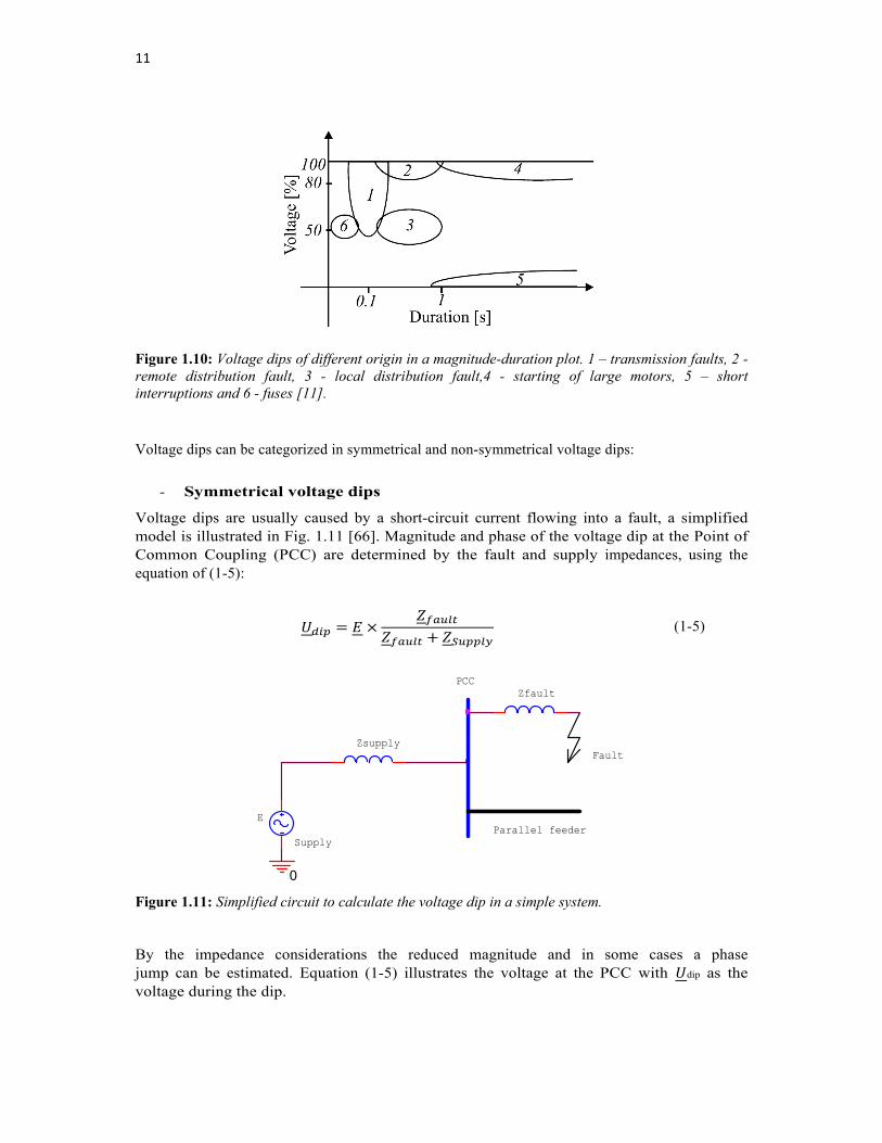
Voltage dips are in many references stated as the most important and costly power quality problem, because of the high risk of tripping devices and a relative frequent occurrence [35],[36]. Voltage dips have been discussed in a large number of papers for instance [20], [37], [38], [39] and [40]. Voltage dips are mainly caused by faults in the grid and the fault clearing time of various protection devices decides the dip duration time. Fig. 1.10 illustrates how the voltage disturbances typically are located in terms of magnitude versus duration. The numbers are referring to the following origin [11]:
1. Transmission system faults; 2. Remote distribution system faults; 3. Local distribution system faults; 4. Starting of large motors; 5. Short interruptions; 6. Fuses;
11
Figure 1.10: Voltage dips of different origin in a magnitude-duration plot. 1 – transmission faults, 2 - remote distribution fault, 3 - local distribution fault,4 - starting of large motors, 5 – short interruptions and 6 - fuses [11].
Voltage dips can be categorized in symmetrical and non-symmetrical voltage dips:
- Symmetrical voltage dips
Voltage dips are usually caused by a short-circuit current flowing into a fault, a simplified model is illustrated in Fig. 1.11 [66]. Magnitude and phase of the voltage dip at the Point of Common Coupling (PCC) are determined by the fault and supply impedances, using the equation of (1-5):
(1-5)
Figure 1.11: Simplified circuit to calculate the voltage dip in a simple system.
By the impedance considerations the reduced magnitude and in some cases a phase jump can be estimated. Equation (1-5) illustrates the voltage at the PCC with dip as the voltage during the dip.
0
Parallel feederE
Zsupply
Zfault
Fault
PCC
Supply
12
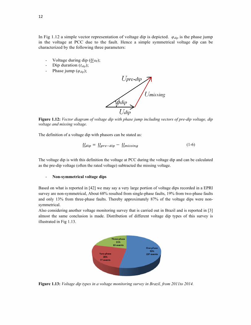
In Fig 1.12 a simple vector representation of voltage dip is depicted. φdip is the phase jump in the voltage at PCC due to the fault. Hence a simple symmetrical voltage dip can be characterized by the following three parameters:
- Voltage during dip ( dip); - Dip duration (tdip); - Phase jump (φdip);
Figure 1.12: Vector diagram of voltage dip with phase jump including vectors of pre-dip voltage, dip voltage and missing voltage. The definition of a voltage dip with phasors can be stated as:
(1-6)
The voltage dip is with this definition the voltage at PCC during the voltage dip and can be calculated as the pre-dip voltage (often the rated voltage) subtracted the missing voltage.
- Non-symmetrical voltage dips
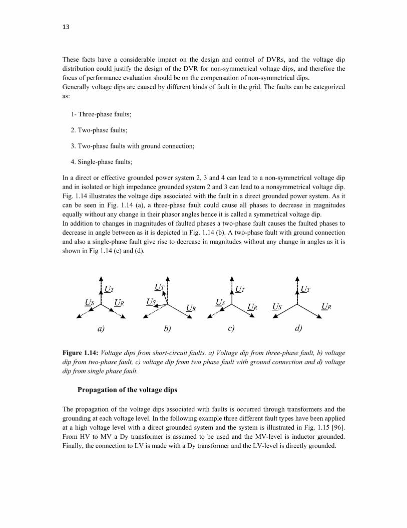
Based on what is reported in [42] we may say a very large portion of voltage dips recorded in a EPRI survey are non-symmetrical, About 68% resulted from single-phase faults, 19% from two-phase faults and only 13% from three-phase faults. Thereby approximately 87% of the voltage dips were non-symmetrical. Also considering another voltage monitoring survey that is carried out in Brazil and is reported in [3] almost the same conclusion is made. Distribution of different voltage dip types of this survey is illustrated in Fig 1.13.
Figure 1.13: Voltage dip types in a voltage monitoring survey in Brazil, from 2011to 2014.
13
These facts have a considerable impact on the design and control of DVRs, and the voltage dip distribution could justify the design of the DVR for non-symmetrical voltage dips, and therefore the focus of performance evaluation should be on the compensation of non-symmetrical dips. Generally voltage dips are caused by different kinds of fault in the grid. The faults can be categorized as:
1- Three-phase faults;
2. Two-phase faults;
3. Two-phase faults with ground connection;
4. Single-phase faults;
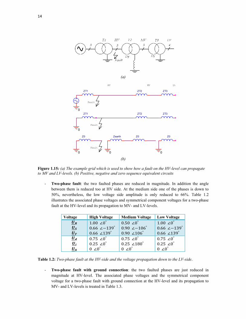
In a direct or effective grounded power system 2, 3 and 4 can lead to a non-symmetrical voltage dip and in isolated or high impedance grounded system 2 and 3 can lead to a nonsymmetrical voltage dip. Fig. 1.14 illustrates the voltage dips associated with the fault in a direct grounded power system. As it can be seen in Fig. 1.14 (a), a three-phase fault could cause all phases to decrease in magnitudes equally without any change in their phasor angles hence it is called a symmetrical voltage dip. In addition to changes in magnitudes of faulted phases a two-phase fault causes the faulted phases to decrease in angle between as it is depicted in Fig. 1.14 (b). A two-phase fault with ground connection and also a single-phase fault give rise to decrease in magnitudes without any change in angles as it is shown in Fig 1.14 (c) and (d).
Figure 1.14: Voltage dips from short-circuit faults. a) Voltage dip from three-phase fault, b) voltage dip from two-phase fault, c) voltage dip from two phase fault with ground connection and d) voltage dip from single phase fault.
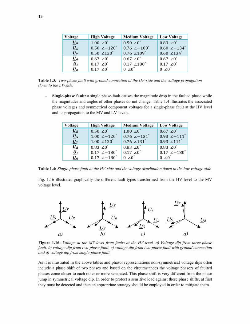
Propagation of the voltage dips The propagation of the voltage dips associated with faults is occurred through transformers and the grounding at each voltage level. In the following example three different fault types have been applied at a high voltage level with a direct grounded system and the system is illustrated in Fig. 1.15 [96]. From HV to MV a Dy transformer is assumed to be used and the MV-level is inductor grounded. Finally, the connection to LV is made with a Dy transformer and the LV-level is directly grounded.
14
(a)
(b)
Figure 1.15: (a) The example grid which is used to show how a fault on the HV-level can propagate to MV and LV-levels. (b) Positive, negative and zero sequence equivalent circuits
- Two-phase fault: the two faulted phases are reduced in magnitude. In addition the angle between them is reduced too at HV side. At the medium side one of the phases is down to 50%, nevertheless, the low voltage side amplitude is only reduced to 66%. Table 1.2 illustrates the associated phase voltages and symmetrical component voltages for a two-phase fault at the HV-level and its propagation to MV- and LV-levels.
Voltage High Voltage Medium Voltage Low Voltage
1.00∠0° 0.66∠ 139° 0.66∠139°
0.50 ∠0° 0.90 ∠ 106° 0.90 ∠106°
1.00 ∠0° 0.66 ∠ 139° 0.66 ∠139°
0.75∠0° 0.25∠0° 0∠0°
0.75 ∠0° 0.25 ∠180° 0 ∠0°
0.75 ∠0° 0.25 ∠0° 0 ∠0°
Table 1.2: Two-phase fault at the HV-side and the voltage propagation down to the LV-side.
- Two-phase fault with ground connection: the two faulted phases are just reduced in magnitude at HV-level. The associated phase voltages and the symmetrical component voltage for a two-phase fault with ground connection at the HV-level and its propagation to MV- and LV-levels is treated in Table 1.3.
Zearth Z0 Z0
00
Z0
0
HV LVMV
ZT1 ZT2 ZT3
0ZT1 ZT2 ZT3
0
Fault
Fault
Fault
15
Voltage High Voltage Medium Voltage Low Voltage
1.00∠0° 0.50∠ 120° 0.50∠120°
0.50 ∠0° 0.76 ∠ 109° 0.76 ∠109°
0.83 ∠0° 0.60 ∠ 134° 0.60 ∠134°
0.67∠0° 0.17∠0° 0.17∠0°
0.67 ∠0° 0.17 ∠180° 0 ∠0°
0.67 ∠0° 0.17 ∠0° 0 ∠0°
Table 1.3: Two-phase fault with ground connection at the HV-side and the voltage propagation down to the LV-side.
- Single-phase fault: a single phase-fault causes the magnitude drop in the faulted phase while the magnitudes and angles of other phases do not change. Table 1.4 illustrates the associated phase voltages and symmetrical component voltages for a single-phase fault at the HV level and its propagation to the MV and LV-levels.
Voltage High Voltage Medium Voltage Low Voltage
0.50∠0° 1.00∠ 120° 1.00∠120°
1.00 ∠0° 0.76 ∠ 131° 0.76 ∠131°
0.67 ∠0° 0.93 ∠ 111° 0.93 ∠111°
0.83∠0° 0.17∠ 180° 0.17∠ 180°
0.83 ∠0° 0.17 ∠0° 0 ∠0°
0.83 ∠0° 0.17 ∠ 180° 0 ∠0°
Table 1.4: Single-phase fault at the HV-side and the voltage distribution down to the low voltage side Fig. 1.16 illustrates graphically the different fault types transformed from the HV-level to the MV voltage level.
Figure 1.16: Voltage at the MV-level from faults at the HV-level. a) Voltage dip from three-phase fault, b) voltage dip from two-phase fault, c) voltage dip from two-phase fault with ground connection and d) voltage dip from single-phase fault. As it is illustrated in the above tables and phasor representations non-symmetrical voltage dips often include a phase shift of two phases and based on the circumstances the voltage phasors of faulted phases come closer to each other or more separated. This phase-shift is very different from the phase jump in symmetrical voltage dip. In order to protect a sensitive load against these phase shifts, at first they must be detected and then an appropriate strategy should be employed in order to mitigate them.
16
1.3 Interruptions
In the European standard EN 50160 two terms are used:
• Long interruptions: longer than three minutes.
• Short interruptions: up to three minutes.
Interruptions are typically caused by different types of faults e.g. malfunction of protection equipment or lightning. In a system without redundancy a fault often leads to a long interruption, which requires manual intervention. Short interruptions are often caused by automatic reclosing after a fault. Short interruptions below three minutes are normally considered a voltage quality problem. Interruptions are a severe power quality problem, but in a wide range of industrial countries interruptions occur very rare, because of redundancy and high maintenance of the grid. A correlation can be found between interruptions and voltage dips. Taking measures to decrease the number of interruptions may increase the number of voltage dips. For instance by having a meshed distribution system (high redundancy) the number of interruptions go down, but the voltage dips can occur more frequently and be more severe [11].
1.4 Power electronic possible solutions for mitigation of voltage dips
The section gives a short survey of three possible power electronic configurations to mitigate voltage dips also treated in [45]. First, shunt controllers are treated, thereafter series controllers and finally combined series/shunt controllers.
1.4.1 Shunt devices
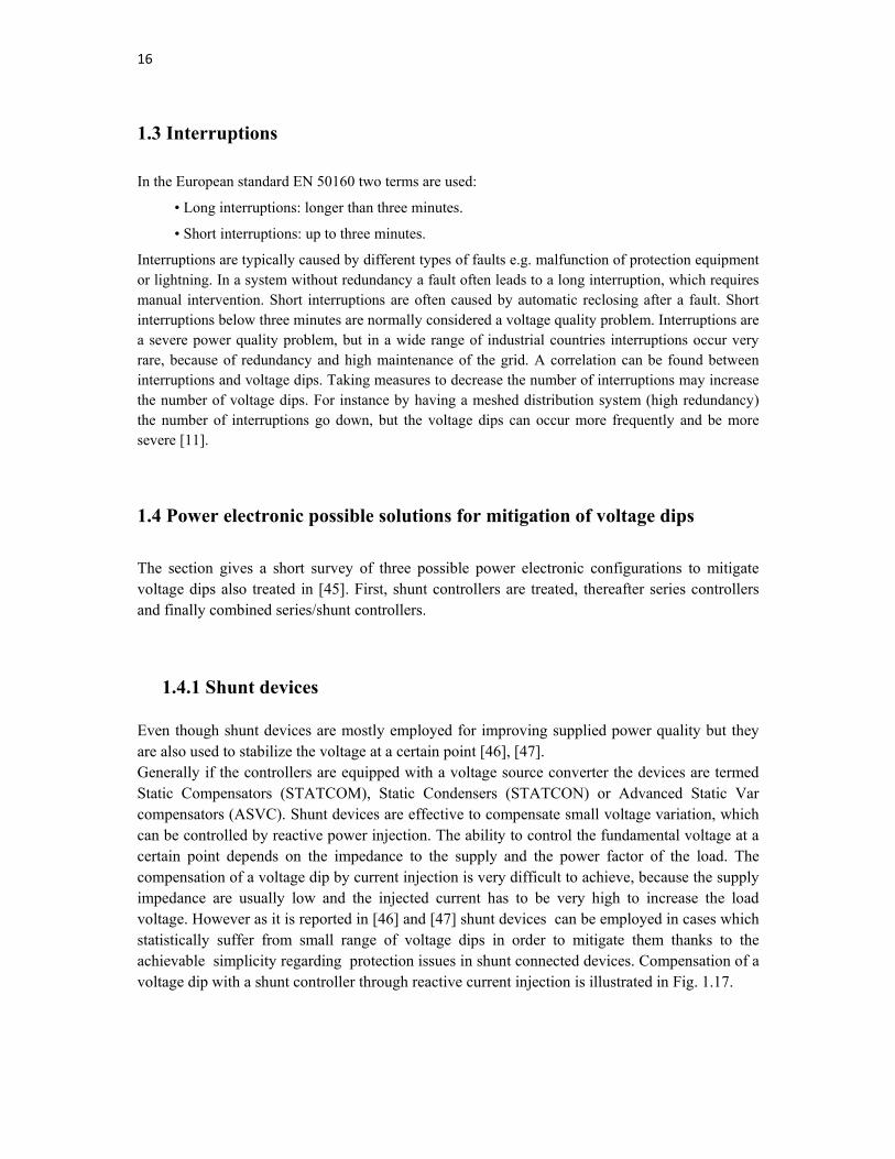
Even though shunt devices are mostly employed for improving supplied power quality but they are also used to stabilize the voltage at a certain point [46], [47]. Generally if the controllers are equipped with a voltage source converter the devices are termed Static Compensators (STATCOM), Static Condensers (STATCON) or Advanced Static Var compensators (ASVC). Shunt devices are effective to compensate small voltage variation, which can be controlled by reactive power injection. The ability to control the fundamental voltage at a certain point depends on the impedance to the supply and the power factor of the load. The compensation of a voltage dip by current injection is very difficult to achieve, because the supply impedance are usually low and the injected current has to be very high to increase the load voltage. However as it is reported in [46] and [47] shunt devices can be employed in cases which statistically suffer from small range of voltage dips in order to mitigate them thanks to the achievable simplicity regarding protection issues in shunt connected devices. Compensation of a voltage dip with a shunt controller through reactive current injection is illustrated in Fig. 1.17.
17
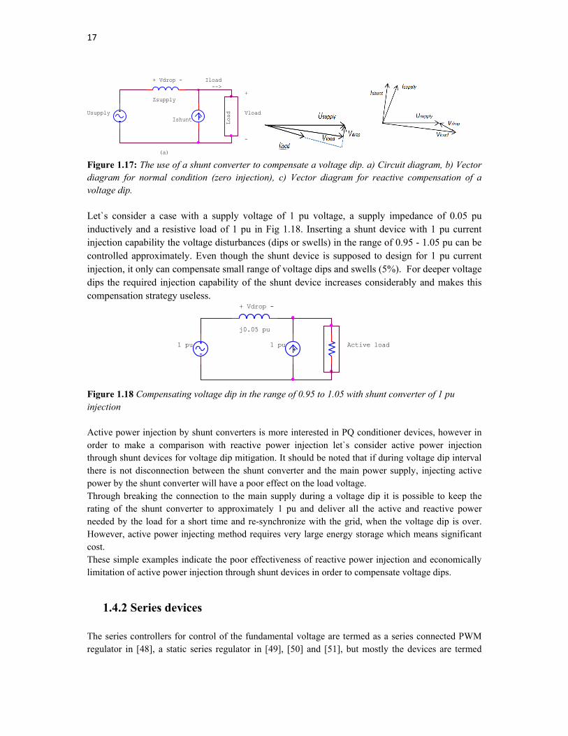
Figure 1.17: The use of a shunt converter to compensate a voltage dip. a) Circuit diagram, b) Vector diagram for normal condition (zero injection), c) Vector diagram for reactive compensation of a voltage dip. Let`s consider a case with a supply voltage of 1 pu voltage, a supply impedance of 0.05 pu inductively and a resistive load of 1 pu in Fig 1.18. Inserting a shunt device with 1 pu current injection capability the voltage disturbances (dips or swells) in the range of 0.95 - 1.05 pu can be controlled approximately. Even though the shunt device is supposed to design for 1 pu current injection, it only can compensate small range of voltage dips and swells (5%). For deeper voltage dips the required injection capability of the shunt device increases considerably and makes this compensation strategy useless.
Figure 1.18 Compensating voltage dip in the range of 0.95 to 1.05 with shunt converter of 1 pu injection Active power injection by shunt converters is more interested in PQ conditioner devices, however in order to make a comparison with reactive power injection let`s consider active power injection through shunt devices for voltage dip mitigation. It should be noted that if during voltage dip interval there is not disconnection between the shunt converter and the main power supply, injecting active power by the shunt converter will have a poor effect on the load voltage. Through breaking the connection to the main supply during a voltage dip it is possible to keep the rating of the shunt converter to approximately 1 pu and deliver all the active and reactive power needed by the load for a short time and re-synchronize with the grid, when the voltage dip is over. However, active power injecting method requires very large energy storage which means significant cost. These simple examples indicate the poor effectiveness of reactive power injection and economically limitation of active power injection through shunt devices in order to compensate voltage dips.
1.4.2 Series devices The series controllers for control of the fundamental voltage are termed as a series connected PWM regulator in [48], a static series regulator in [49], [50] and [51], but mostly the devices are termed
+-
Load
Iload
IshuntUsupply
Zsupply
Vload
+
-
-->
(a)
+ -Vdrop
+-1 pu1 pu
j0.05 pu
Active load
+ -Vdrop
18
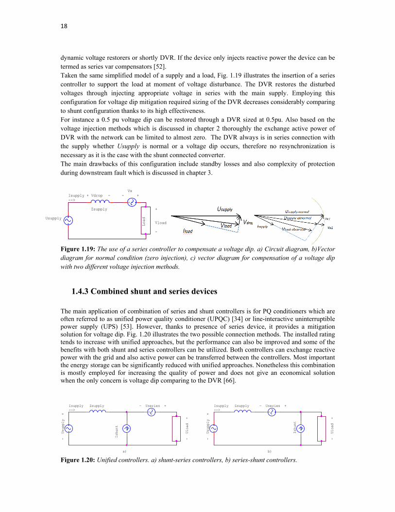
dynamic voltage restorers or shortly DVR. If the device only injects reactive power the device can be termed as series var compensators [52]. Taken the same simplified model of a supply and a load, Fig. 1.19 illustrates the insertion of a series controller to support the load at moment of voltage disturbance. The DVR restores the disturbed voltages through injecting appropriate voltage in series with the main supply. Employing this configuration for voltage dip mitigation required sizing of the DVR decreases considerably comparing to shunt configuration thanks to its high effectiveness. For instance a 0.5 pu voltage dip can be restored through a DVR sized at 0.5pu. Also based on the voltage injection methods which is discussed in chapter 2 thoroughly the exchange active power of DVR with the network can be limited to almost zero. The DVR always is in series connection with the supply whether Usupply is normal or a voltage dip occurs, therefore no resynchronization is necessary as it is the case with the shunt connected converter. The main drawbacks of this configuration include standby losses and also complexity of protection during downstream fault which is discussed in chapter 3.
Figure 1.19: The use of a series controller to compensate a voltage dip. a) Circuit diagram, b)Vector diagram for normal condition (zero injection), c) vector diagram for compensation of a voltage dip with two different voltage injection methods.
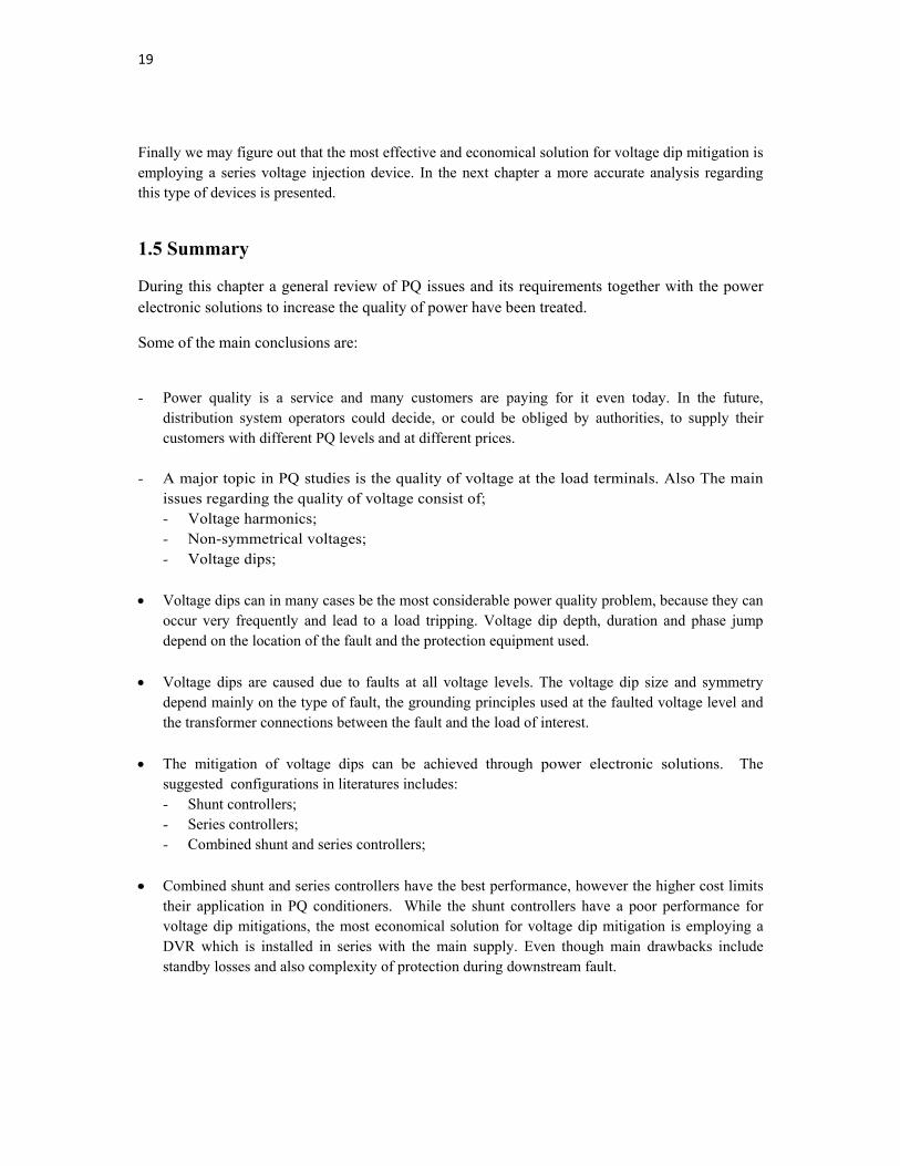
1.4.3 Combined shunt and series devices The main application of combination of series and shunt controllers is for PQ conditioners which are often referred to as unified power quality conditioner (UPQC) [34] or line-interactive uninterruptible power supply (UPS) [53]. However, thanks to presence of series device, it provides a mitigation solution for voltage dip. Fig. 1.20 illustrates the two possible connection methods. The installed rating tends to increase with unified approaches, but the performance can also be improved and some of the benefits with both shunt and series controllers can be utilized. Both controllers can exchange reactive power with the grid and also active power can be transferred between the controllers. Most important the energy storage can be significantly reduced with unified approaches. Nonetheless this combination is mostly employed for increasing the quality of power and does not give an economical solution when the only concern is voltage dip comparing to the DVR [66].
Figure 1.20: Unified controllers. a) shunt-series controllers, b) series-shunt controllers.
Ishu
nt
Ishunt
+-
Isupply
- U
load
+
-->Zsupply
- U
supp
ly
+
- Useries +
b)a)
+-
Isupply-->
- U
load
+
- U
supp
ly
+
Zsupply - Useries +
Isupply-->
Usupply
Load
-+ VdropVx
+-
Zsupply +
-
Vload
19
Finally we may figure out that the most effective and economical solution for voltage dip mitigation is employing a series voltage injection device. In the next chapter a more accurate analysis regarding this type of devices is presented.
1.5 Summary
During this chapter a general review of PQ issues and its requirements together with the power electronic solutions to increase the quality of power have been treated.
Some of the main conclusions are:
- Power quality is a service and many customers are paying for it even today. In the future,
distribution system operators could decide, or could be obliged by authorities, to supply their customers with different PQ levels and at different prices.
- A major topic in PQ studies is the quality of voltage at the load terminals. Also The main
issues regarding the quality of voltage consist of; - Voltage harmonics; - Non-symmetrical voltages; - Voltage dips;
Voltage dips can in many cases be the most considerable power quality problem, because they can occur very frequently and lead to a load tripping. Voltage dip depth, duration and phase jump depend on the location of the fault and the protection equipment used.
Voltage dips are caused due to faults at all voltage levels. The voltage dip size and symmetry depend mainly on the type of fault, the grounding principles used at the faulted voltage level and the transformer connections between the fault and the load of interest.
The mitigation of voltage dips can be achieved through power electronic solutions. The suggested configurations in literatures includes: - Shunt controllers; - Series controllers; - Combined shunt and series controllers;
Combined shunt and series controllers have the best performance, however the higher cost limits their application in PQ conditioners. While the shunt controllers have a poor performance for voltage dip mitigations, the most economical solution for voltage dip mitigation is employing a DVR which is installed in series with the main supply. Even though main drawbacks include standby losses and also complexity of protection during downstream fault.
20
CHAPTER 2
Analysis of dynamic voltage restorer
During this chapter a general review of a DVR and its constituent parts, placement options within the grid and possible topologies to realize a DVR are presented. More details on rating values of a DVR, sizing a DVR and designing the control systems are treated in the appendix.
2.1 General configuration and elements of a DVR
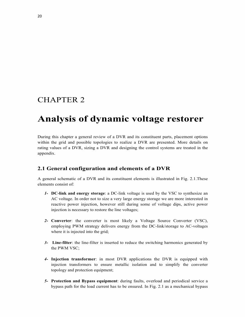
A general schematic of a DVR and its constituent elements is illustrated in Fig. 2.1.These elements consist of:
1- DC-link and energy storage: a DC-link voltage is used by the VSC to synthesize an AC voltage. In order not to size a very large energy storage we are more interested in reactive power injection, however still during some of voltage dips, active power injection is necessary to restore the line voltages;
2- Converter: the converter is most likely a Voltage Source Converter (VSC), employing PWM strategy delivers energy from the DC-link/storage to AC-voltages where it is injected into the grid;
3- Line-filter: the line-filter is inserted to reduce the switching harmonics generated by the PWM VSC;
4- Injection transformer: in most DVR applications the DVR is equipped with injection transformers to ensure metallic isolation and to simplify the converter topology and protection equipment;
5- Protection and Bypass equipment: during faults, overload and periodical service a bypass path for the load current has to be ensured. In Fig. 2.1 as a mechanical bypass
21
together with a static switch bypass is illustrated. Also fault current limiting function is an issue of interest in some cases and possible solutions for that will be considered in the next chapter;
6- Control and measuring unit: this unit measures voltages and currents and controls VSC of the DVR to produce appropriate voltage in order to compensate voltage dips. Also this unit controls the static switch bypass for bypassing the DVR when it is required;
7- Disconnection equipment: to completely disconnect the DVR for periodical service;
Figure 2.1: The basic elements of a DVR in a single-line representation.
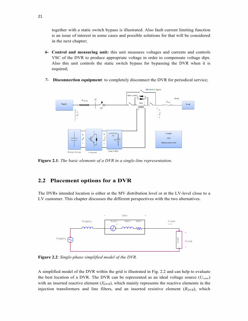
2.2 Placement options for a DVR The DVRs intended location is either at the MV distribution level or at the LV-level close to a LV customer. This chapter discusses the different perspectives with the two alternatives.
Figure 2.2: Single-phase simplified model of the DVR.
A simplified model of the DVR within the grid is illustrated in Fig. 2.2 and can help to evaluate the best location of a DVR. The DVR can be represented as an ideal voltage source (Uconv)
with an inserted reactive element (XDVR), which mainly represents the reactive elements in the injection transformers and line filters, and an inserted resistive element (RDVR), which
LoadUsupply
- +UconvZsupply
Uload
-
+
Iload-->
Xdvr Rdvr
- +Udvr
22
represents the losses in the DVR. The size of the inserted impedance is closely related to the DVR voltage rating (UDVR) and the DVR power rating (SDVR) according to:
,
(2.1)
,
(2.2)
,
(2.3)
, , , (2.4)
uDVR,Z depends on the type of transformer used, the line-filter, losses in the
VSC etc. A DVR with high injection capability (high UDVR) and the ability only to protect a small load (low SDVR) has large equivalent DVR impedance (ZDVR).
Going from a LV-level DVR to a higher voltage level DVR the pu value of the
reactance (uDVR,X) tends to increase, and the pu value resistance (uDVR,R) tends to
decrease. A high resistive part increases the energy which is dissipated through the DVR and the costs associated with the losses. High total inserted DVR impedance increases the potential load voltage distortion and load voltage fluctuations if the load is non-linear and/or has a fluctuating load behavior.
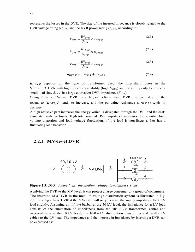
2.2.1 MV-level DVR
Figure 2.3: DVR located at the medium voltage distribution system
Applying the DVR to the MV-level, it can protect a large consumer or a group of consumers. The insertion of a DVR in the medium voltage distribution system is illustrated in Fig. 2.3. Inserting a large DVR at the MV-level will only increase the supply impedance for a LV load slightly. Assuming an infinite busbar at the 50 kV level, the impedance for a LV load consists of the summation of impedances from the 50/10 kV transformer, cables and overhead lines at the 10 kV level, the 10/0.4 kV distribution transformer and finally LV cables to the LV load. The impedance and the increase in impedance by inserting a DVR can be expressed as:
3 3 33
3
3
4
4
4MV DVR
50/10 kV10/0.4kV
23
, / , / , . (2.5)
, ,
(2.6)
,%,
100%
(2.7)
For a LV load the dominant impedance is most likely the LV-line impedance
(Zline,0.4) and the impedance of the distribution transformer (Z10/0.4) not . Even though for a large MV-load close to the DVR the increase in impedance due to insertion of the DVR can be significant.
Inserting one high rated DVR at the MV-level has certain advantages:
The increased impedance due to DVR insertion seen by a LV-load can be relative small if a large DVR is placed at the MV-level;
In MV-distribution systems which are configured as a three-wire system with isolated or inductor grounded system, injection of positive and negative sequence system is sufficient and a simpler DVR topology and hardware can be used;
The costs per MVA to protect downstream loads against voltage dips are expected to be lower if one large central DVR is located at the medium voltage level instead of decentralized low voltage units;
Some of the disadvantages can be summarized to:
The DVR is connected to a higher voltage level, which requires a high isolation level and the short circuit level is also high;
Protecting a large load may require a DVR with high voltage injection capability (UDVR) otherwise the losses in the DVR will be too high;
A part of the DVR rating may be utilized on less sensitive loads which do not require a high voltage quality;
2.2.2 LV-level DVR
The insertion of a DVR at the low voltage four-wire 400 V level is illustrated in Fig. 2.4. The increase in impedance by insertion of a small rated DVR can be significant for the load to be protected from voltage dips. Thereby, the percent change in the impedance ( ,%) in (2.7) can be increased significantly.
24
3 3
3
3
450/10 kV
10/0.4kVLV DVR
4
3 4
3 43
Targeted LV loads
44
Figure 2.4: DVR located at the low voltage distribution system.
Inserting a DVR at LV-level has certain advantages:
The DVR can be targeted more specifically at voltage dip sensitive loads;
A majority of electric customers have only access to the LV-level and the DVR can both be placed by the customer at the customer domain or by the utility at the utility domain;
The short-circuit level is significantly decreased by the distribution transformer and the DVR is easier to protect;
And the disadvantages with a LV solution are:
The impedance increment after the insertion of the DVR for the protected load can be large, which may influence the site short circuit level and protection. An increased load voltage distortion and load voltage variation can be expected, which may be caused by nonlinear and time varying load currents;
Voltage dips with a zero sequence voltage component can appear and in order to be able to compensate properly, the DVR hardware and control should be able to generate positive, negative and zero sequence voltages;
2.3 Presented schemes for realizing a DVR
During this section the main schemes and topologies for DVRs are discussed with focus on methods to connect the DVR to the grid, converter topologies suited for DVRs and also methods to ensure active power injection capability during the voltage dip mitigation. The section includes a survey and comparison of the different topologies for DVRs, which also have been treated in [54], [55] and [56].
2.3.1 DVR connection to the grid
The DVR is going to inject a voltage in series with the supply, which requires either metallic isolation to the VSC or letting the VSC float at the potential of the supply voltages. Two different approaches are here considered, referred to as a transformer connected converter or a transformer-less converter.
25
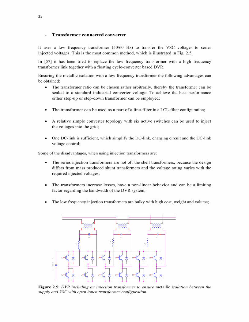
- Transformer connected converter
It uses a low frequency transformer (50/60 Hz) to transfer the VSC voltages to series injected voltages. This is the most common method, which is illustrated in Fig. 2.5.
In [57] it has been tried to replace the low frequency transformer with a high frequency transformer link together with a floating cyclo-converter based DVR.
Ensuring the metallic isolation with a low frequency transformer the following advantages can be obtained:
The transformer ratio can be chosen rather arbitrarily, thereby the transformer can be scaled to a standard industrial converter voltage. To achieve the best performance either step-up or step-down transformer can be employed;
The transformer can be used as a part of a line-filter in a LCL-filter configuration;
A relative simple converter topology with six active switches can be used to inject the voltages into the grid;
One DC-link is sufficient, which simplify the DC-link, charging circuit and the DC-link voltage control;
Some of the disadvantages, when using injection transformers are:
The series injection transformers are not off the shell transformers, because the design differs from mass produced shunt transformers and the voltage rating varies with the required injected voltages;
The transformers increase losses, have a non-linear behavior and can be a limiting factor regarding the bandwidth of the DVR system;
The low frequency injection transformers are bulky with high cost, weight and volume;
Figure 2.5: DVR including an injection transformer to ensure metallic isolation between the supply and VSC with open /open transformer configuration.
Lf
Cf
Lf
CfCf
-
Udc
+
Lf
.
.
.
. .
.
26
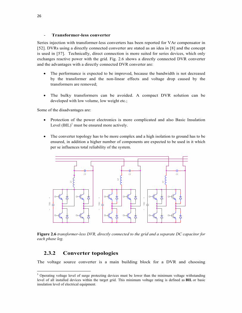
- Transformer-less converter
Series injection with transformer-less converters has been reported for VAr compensator in [52]. DVRs using a directly connected converter are stated as an idea in [8] and the concept is used in [57]. Technically, direct connection is more suited for series devices, which only exchanges reactive power with the grid. Fig. 2.6 shows a directly connected DVR converter and the advantages with a directly connected DVR converter are:
The performance is expected to be improved, because the bandwidth is not decreased by the transformer and the non-linear effects and voltage drop caused by the transformers are removed;
The bulky transformers can be avoided. A compact DVR solution can be developed with low volume, low weight etc.;
Some of the disadvantages are:
Protection of the power electronics is more complicated and also Basic Insulation Level (BIL)1 must be ensured more actively.
The converter topology has to be more complex and a high isolation to ground has to be ensured, in addition a higher number of components are expected to be used in it which per se influences total reliability of the system.
Figure 2.6 transformer-less DVR, directly connected to the grid and a separate DC capacitor for each phase leg.
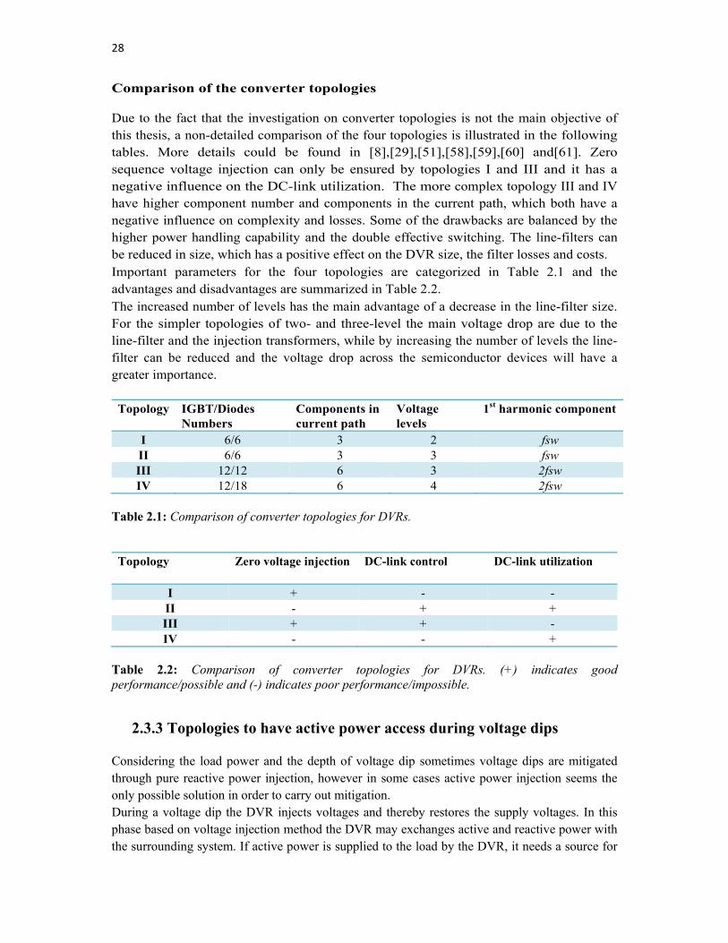
2.3.2 Converter topologies
The voltage source converter is a main building block for a DVR and choosing
1 Operating voltage level of surge protecting devices must be lower than the minimum voltage withstanding level of all installed devices within the target grid. This minimum voltage rating is defined as BIL or basic insulation level of electrical equipment.
Lf
Cf
Lf
Cf
-
Udc
+
-
Udc
+
-
Udc
+
Lf
Cf
27
a topology suited for the application is essential regarding system performance. The DVR is connected in series and the impedances inserted lead to unwanted voltage drops and losses. The treated converter topologies in the following have been limited to transformer connected converters based VSC with hard switching.
The basic converter topologies, which are presented in the literatures include:
Half bridge topologies; - Half bridge converter with an open1 / star transformer connection -Topology
I which is reported in [51] and [58];
- Half bridge converter with an open / delta transformer connection -Topology II which is reported in [29];
Full bridge topology;
- Full bridge converter with an open / open transformer connection -Topology III which is reported in [8];
Multilevel topology; - Half bridge three-level converter with an open/delta transformer
connection-Topology IV which is reported in [59], [60] and [61];
The following parameters must have been included in the investigation and comparison of these mentioned topologies:
The effective switching frequency which influences the size of the line-filter and by having a high effective switching frequency the line-filter can be reduced.
The number of devices in the current path in order to estimate losses and resistive voltage drop across the DVR. Also the number of devices influences reliability, cost and complexity in the system.
Ability to handle zero sequence currents and injection of zero sequence voltages. Compensating zero sequence voltages requires individual control of each phase and only certain topologies can comply with this.
Utilization of the DC-link voltage.
Control of the DC-link voltage and methods to transfer active power to/from the DC-link.
These above parameters are very relevant concepts regarding converter parameters for DVR applications and they must be considered in order to select appropriate converter topology.
1“Open” term is referring to the configuration of three separate (magnetically de‐coupled) single phase transformers
28
Comparison of the converter topologies
Due to the fact that the investigation on converter topologies is not the main objective of this thesis, a non-detailed comparison of the four topologies is illustrated in the following tables. More details could be found in [8],[29],[51],[58],[59],[60] and[61]. Zero sequence voltage injection can only be ensured by topologies I and III and it has a negative influence on the DC-link utilization. The more complex topology III and IV have higher component number and components in the current path, which both have a negative influence on complexity and losses. Some of the drawbacks are balanced by the higher power handling capability and the double effective switching. The line-filters can be reduced in size, which has a positive effect on the DVR size, the filter losses and costs. Important parameters for the four topologies are categorized in Table 2.1 and the advantages and disadvantages are summarized in Table 2.2. The increased number of levels has the main advantage of a decrease in the line-filter size. For the simpler topologies of two- and three-level the main voltage drop are due to the line-filter and the injection transformers, while by increasing the number of levels the line-filter can be reduced and the voltage drop across the semiconductor devices will have a greater importance. Topology IGBT/Diodes
Numbers Components in current path
Voltage levels
1st harmonic component
I 6/6 3 2 fsw II 6/6 3 3 fsw III 12/12 6 3 2fsw IV 12/18 6 4 2fsw
Table 2.1: Comparison of converter topologies for DVRs. Topology Zero voltage injection
DC-link control DC-link utilization
I + - - II - + + III + + - IV - - +
Table 2.2: Comparison of converter topologies for DVRs. (+) indicates good performance/possible and (-) indicates poor performance/impossible.
2.3.3 Topologies to have active power access during voltage dips Considering the load power and the depth of voltage dip sometimes voltage dips are mitigated through pure reactive power injection, however in some cases active power injection seems the only possible solution in order to carry out mitigation. During a voltage dip the DVR injects voltages and thereby restores the supply voltages. In this phase based on voltage injection method the DVR may exchanges active and reactive power with the surrounding system. If active power is supplied to the load by the DVR, it needs a source for

29
the energy. Two concepts are here considered, one concept uses stored energy and the other concept uses no significant energy storage. The stored energy can be delivered from different kinds of energy storage systems such as batteries [62], double-layer-capacitors [63], super-capacitors, flywheel storage [64] or SMES. In the no-storage DVR concept, the DVR has practically no energy storage and the energy is taken from the remaining supply voltage during the voltage dip. The four system topologies, which are presented and compared, are:
Topologies with stored energy devices – Constant DC-link voltage; – Variable DC-link voltage;
Topologies with power from the supply – Supply side connected passive shunt converter; – Load side connected passive shunt converter;
The parameters, which have been focused on in the comparison are:
DC-link voltage level and control during voltage dips;
Rating of the converters used for the DVR solution;
Ability to compensate voltage dips of different kinds;
Effect on the supply and neighboring loads;
System and control complexity;
Relative cost estimations; In order to simplify and clarify the comparison the load is assumed to be purely resistive and to absorb rated active power and the load voltages are always restored to rated load voltage. This can be stated as:
Pload = Pload,rated, φload = 0, Uload = Uload,rated (2.8)
The voltage dips, which are considered, are symmetrical, have no phase jump and the DVR injects only a voltage in phase with the supply voltage:
Udip,non−symmetry% = 0, φdip = 0, φDV R = φsupply (2.9)
Some values and equations have been transferred to pu values with rated load voltage as base voltage and the rated three-phase load power as the base power. pu values are indicated with lower-case letters. Topologies with stored energy In this case all the energy is stored before the voltage dip and a very small scale converter is expected to be used to re-charge the energy storage or employing the diodes in the VSC during
30
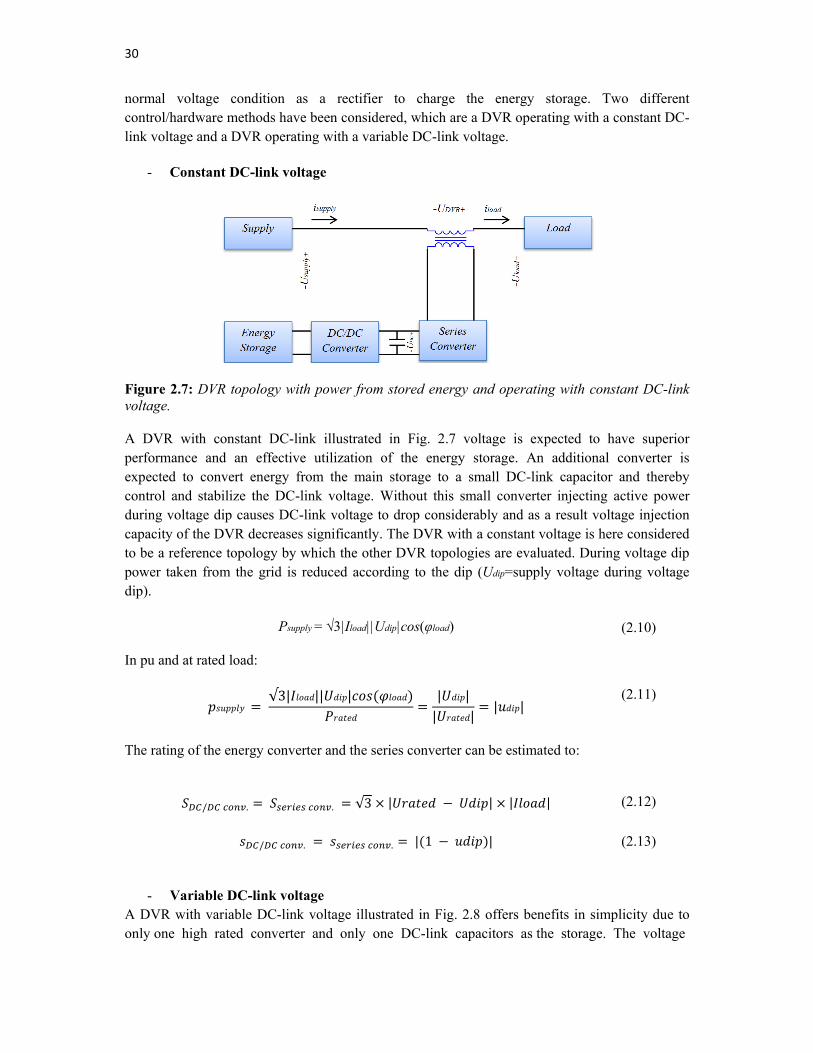
normal voltage condition as a rectifier to charge the energy storage. Two different control/hardware methods have been considered, which are a DVR operating with a constant DC-link voltage and a DVR operating with a variable DC-link voltage.
- Constant DC-link voltage
Figure 2.7: DVR topology with power from stored energy and operating with constant DC-link voltage. A DVR with constant DC-link illustrated in Fig. 2.7 voltage is expected to have superior performance and an effective utilization of the energy storage. An additional converter is expected to convert energy from the main storage to a small DC-link capacitor and thereby control and stabilize the DC-link voltage. Without this small converter injecting active power during voltage dip causes DC-link voltage to drop considerably and as a result voltage injection capacity of the DVR decreases significantly. The DVR with a constant voltage is here considered to be a reference topology by which the other DVR topologies are evaluated. During voltage dip power taken from the grid is reduced according to the dip (Udip=supply voltage during voltage dip).
Psupply = √3|Iload||Udip|cos(φload)
(2.10)
In pu and at rated load:
√3| || | | |
| || |
(2.11)
The rating of the energy converter and the series converter can be estimated to:
/ . . √3 | | | |
(2.12)
/ . . | 1 |
(2.13)
- Variable DC-link voltage
A DVR with variable DC-link voltage illustrated in Fig. 2.8 offers benefits in simplicity due to only one high rated converter and only one DC-link capacitors as the storage. The voltage
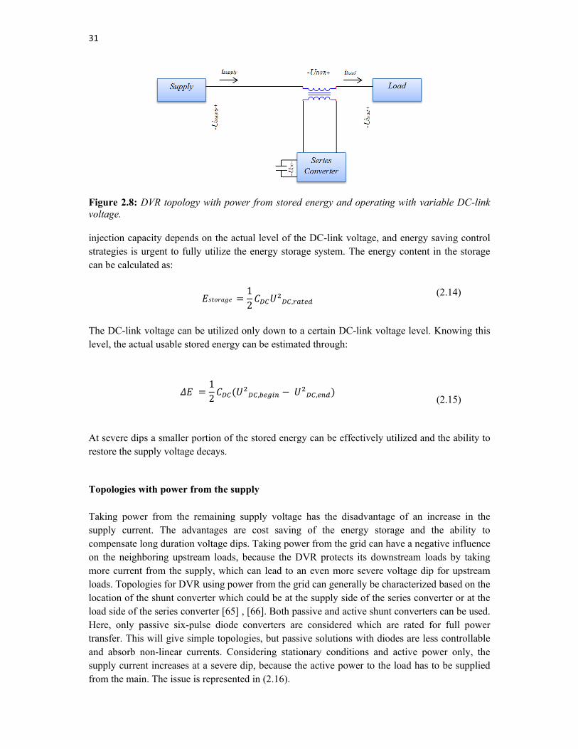
31
Figure 2.8: DVR topology with power from stored energy and operating with variable DC-link voltage. injection capacity depends on the actual level of the DC-link voltage, and energy saving control strategies is urgent to fully utilize the energy storage system. The energy content in the storage can be calculated as:
12 ,
(2.14)
The DC-link voltage can be utilized only down to a certain DC-link voltage level. Knowing this level, the actual usable stored energy can be estimated through:
12 , ,
(2.15)
At severe dips a smaller portion of the stored energy can be effectively utilized and the ability to restore the supply voltage decays. Topologies with power from the supply
Taking power from the remaining supply voltage has the disadvantage of an increase in the supply current. The advantages are cost saving of the energy storage and the ability to compensate long duration voltage dips. Taking power from the grid can have a negative influence on the neighboring upstream loads, because the DVR protects its downstream loads by taking more current from the supply, which can lead to an even more severe voltage dip for upstream loads. Topologies for DVR using power from the grid can generally be characterized based on the location of the shunt converter which could be at the supply side of the series converter or at the load side of the series converter [65] , [66]. Both passive and active shunt converters can be used. Here, only passive six-pulse diode converters are considered which are rated for full power transfer. This will give simple topologies, but passive solutions with diodes are less controllable and absorb non-linear currents. Considering stationary conditions and active power only, the supply current increases at a severe dip, because the active power to the load has to be supplied from the main. The issue is represented in (2.16).
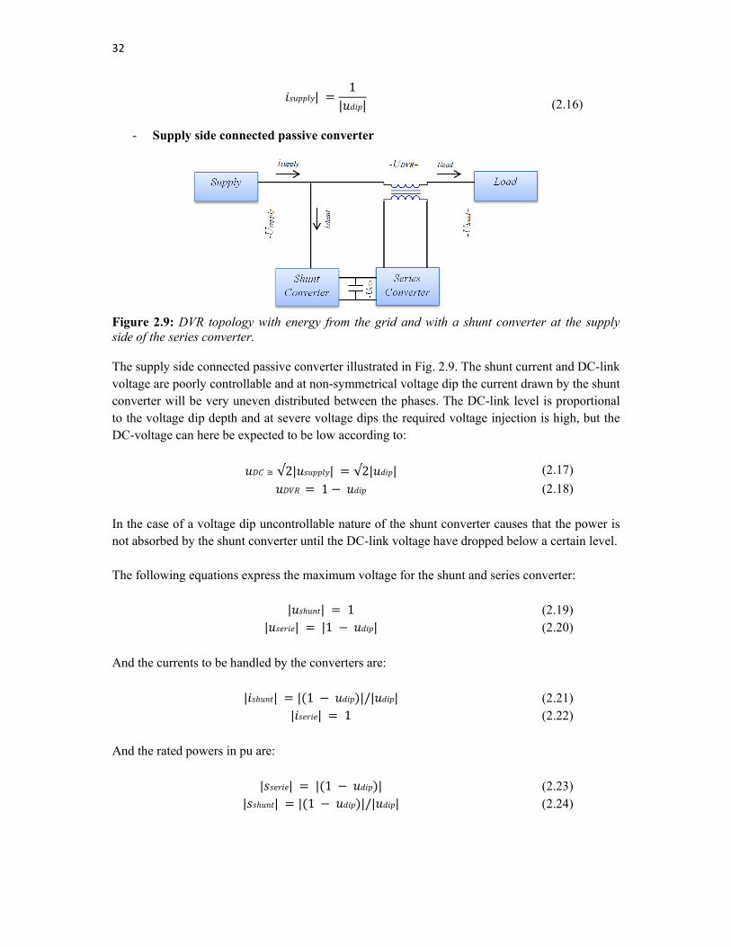
32
|1
| |
(2.16)
- Supply side connected passive converter
Figure 2.9: DVR topology with energy from the grid and with a shunt converter at the supply side of the series converter. The supply side connected passive converter illustrated in Fig. 2.9. The shunt current and DC-link voltage are poorly controllable and at non-symmetrical voltage dip the current drawn by the shunt converter will be very uneven distributed between the phases. The DC-link level is proportional to the voltage dip depth and at severe voltage dips the required voltage injection is high, but the DC-voltage can here be expected to be low according to:
≅ √2| | √2| | (2.17)
1 (2.18)
In the case of a voltage dip uncontrollable nature of the shunt converter causes that the power is not absorbed by the shunt converter until the DC-link voltage have dropped below a certain level. The following equations express the maximum voltage for the shunt and series converter:
| | 1 (2.19) | | |1 | (2.20)
And the currents to be handled by the converters are:
| | | 1 |/| | (2.21) | | 1 (2.22)
And the rated powers in pu are:
| | | 1 | (2.23) | | | 1 |/| | (2.24)
33
The concept of a passive shunt converter is relative cheap, but the correlation between the DC-link voltage and the dip size is unfavorably and expected to be unqualified for severe voltage dip compensation in general.
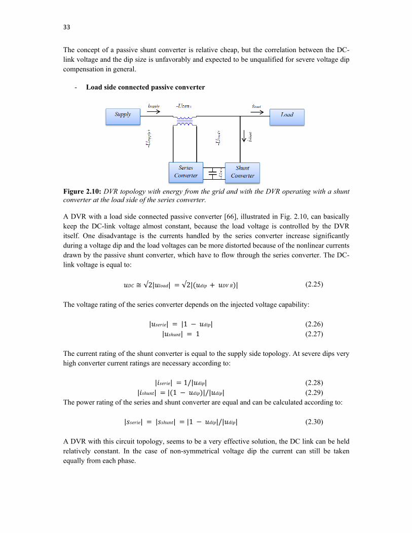
- Load side connected passive converter
Figure 2.10: DVR topology with energy from the grid and with the DVR operating with a shunt converter at the load side of the series converter. A DVR with a load side connected passive converter [66], illustrated in Fig. 2.10, can basically keep the DC-link voltage almost constant, because the load voltage is controlled by the DVR itself. One disadvantage is the currents handled by the series converter increase significantly during a voltage dip and the load voltages can be more distorted because of the nonlinear currents drawn by the passive shunt converter, which have to flow through the series converter. The DC-link voltage is equal to:
≅ √2| | √2| | (2.25)
The voltage rating of the series converter depends on the injected voltage capability:
| | |1 | (2.26) | | 1 (2.27)
The current rating of the shunt converter is equal to the supply side topology. At severe dips very high converter current ratings are necessary according to:
| | 1/| | (2.28) | | | 1 |/| | (2.29)
The power rating of the series and shunt converter are equal and can be calculated according to:
| | | | |1 |/| | (2.30) A DVR with this circuit topology, seems to be a very effective solution, the DC link can be held relatively constant. In the case of non-symmetrical voltage dip the current can still be taken equally from each phase.
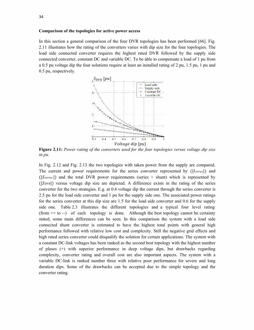
34
Comparison of the topologies for active power access In this section a general comparison of the four DVR topologies has been performed [66]. Fig. 2.11 illustrates how the rating of the converters varies with dip size for the four topologies. The load side connected converter requires the highest rated DVR followed by the supply side connected converter, constant DC and variable DC. To be able to compensate a load of 1 pu from a 0.5 pu voltage dip the four solutions require at least an installed rating of 2 pu, 1.5 pu, 1 pu and 0.5 pu, respectively.
Figure 2.11: Power rating of the converters used for the four topologies versus voltage dip size in pu. In Fig. 2.12 and Fig. 2.13 the two topologies with taken power from the supply are compared. The current and power requirements for the series converter represented by | | and | | and the total DVR power requirements (series + shunt) which is represented by | | versus voltage dip size are depicted. A difference exists in the rating of the series
converter for the two strategies. E.g. at 0.4 voltage dip the current through the series converter is 2.5 pu for the load side converter and 1 pu for the supply side one. The associated power ratings for the series converter at this dip size are 1.5 for the load side converter and 0.6 for the supply side one. Table 2.3 illustrates the different topologies and a typical four level rating (from ++ to --) of each topology is done. Although the best topology cannot be certainty stated, some main differences can be seen. In this comparison the system with a load side connected shunt converter is estimated to have the highest total points with general high performance followed with relative low cost and complexity. Still the negative grid effects and high rated series converter could disqualify the solution for certain applications. The system with a constant DC-link voltages has been ranked as the second best topology with the highest number of pluses (+) with superior performance in deep voltage dips, but drawbacks regarding complexity, converter rating and overall cost are also important aspects. The system with a variable DC-link is ranked number three with relative poor performance for severe and long duration dips. Some of the drawbacks can be accepted due to the simple topology and the converter rating.
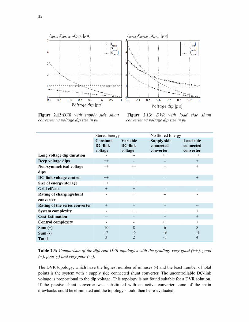
35
Figure 2.12:DVR with supply side shunt converter vs voltage dip size in pu
Figure 2.13: DVR with load side shunt converter vs voltage dip size in pu
Stored Energy No Stored Energy
Constant DC-link voltage
Variable DC-link voltage
Supply side connected converter
Load side connected converter
Long voltage dip duration - -- ++ ++ Deep voltage dips ++ - -- + Non-symmetrical voltage dips
++ ++ -- +
DC-link voltage control ++ - -- + Size of energy storage ++ + Grid effects + + - - Rating of charging/shunt converter
- + -- -
Rating of the series converter + + + -- System complexity - ++ + + Cost Estimation -- - + + Control complexity - - ++ + Sum (+) Sum (-) Total
10 -7 3
8 -6 2
6 -9 -3
8 -4 4
Table 2.3: Comparison of the different DVR topologies with the grading: very good (++), good (+), poor (-) and very poor (- -). The DVR topology, which have the highest number of minuses (-) and the least number of total points is the system with a supply side connected shunt converter. The uncontrollable DC-link voltage is proportional to the dip voltage. This topology is not found suitable for a DVR solution. If the passive shunt converter was substituted with an active converter some of the main drawbacks could be eliminated and the topology should then be re-evaluated.
, , , ,
36
2.4 DVR operation modes
The DVR can basically be operated in three different operation modes, which here are referred to as:
1- Bypass mode: the DVR is bypassed mechanically or electronically, during high load currents and down-stream short circuits. In this mode the DVR cannot inject a voltage to improve the voltage quality;
2- Standby mode: the supply voltages are at rated level and the DVR are ready to
compensate for a voltage dip. During standby mode the DVR is supposed to have low conduction loss;
3- Active mode: A voltage dip has been detected and the DVR injects the missing voltage;
2.5 DVR limitations It is important to address the DVR limitations, which may be closely linked to the control strategy [75]. A DVR has limited capabilities and the DVR will most likely face a voltage dip outside the range of full compensation. Four important limitations for a DVR are:
1- Voltage limit: the design of the DVR is limited in the injection capability to keep the cost down and to reduce the voltage drop across the device in standby operation;
2- Current limit: the DVR has a limitation in current conduction capability to keep the cost
down;
3- Power limit: power is stored in the DC-link, but the bulk power is often converted from the supply itself or from a larger DC storage. An additional converter is often used to maintain a constant DC-link voltage and the rating of the converter can introduce a power limit to the DVR;
4- Energy limit: energy is used to maintain the load voltage constant and the storage is
normally sized as low as possible in order to reduce cost. Some dips will deplete the storage fast, so appropriate control is required to reduce the risk of load tripping caused by insufficient energy storage;
All the limits should be taken into consideration in the control strategy. Fig. 2.14 illustrates a single-phase phasor diagram for DVR limitations. The phasor of the pre-dip voltage is shown with a lagging load current and the voltage dip contains a negative phase jump. The voltage and power limits are indicated and the hatched region illustrates the region which the DVR can operate within. The pre-dip voltage cannot be maintained in the case illustrated in Fig. 2.14.
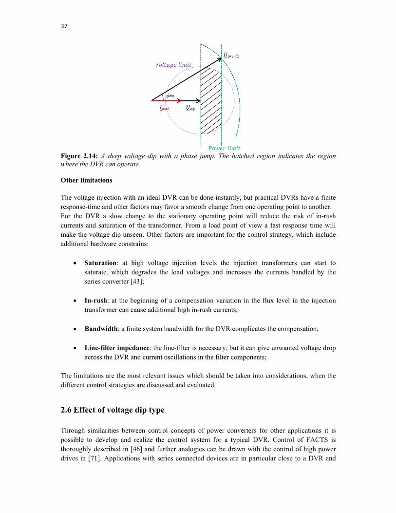
37
Figure 2.14: A deep voltage dip with a phase jump. The hatched region indicates the region where the DVR can operate. Other limitations The voltage injection with an ideal DVR can be done instantly, but practical DVRs have a finite response-time and other factors may favor a smooth change from one operating point to another. For the DVR a slow change to the stationary operating point will reduce the risk of in-rush currents and saturation of the transformer. From a load point of view a fast response time will make the voltage dip unseen. Other factors are important for the control strategy, which include additional hardware constrains:
Saturation: at high voltage injection levels the injection transformers can start to saturate, which degrades the load voltages and increases the currents handled by the series converter [43];
In-rush: at the beginning of a compensation variation in the flux level in the injection transformer can cause additional high in-rush currents;
Bandwidth: a finite system bandwidth for the DVR complicates the compensation;
Line-filter impedance: the line-filter is necessary, but it can give unwanted voltage drop across the DVR and current oscillations in the filter components;
The limitations are the most relevant issues which should be taken into considerations, when the different control strategies are discussed and evaluated.
2.6 Effect of voltage dip type
Through similarities between control concepts of power converters for other applications it is possible to develop and realize the control system for a typical DVR. Control of FACTS is thoroughly described in [46] and further analogies can be drawn with the control of high power drives in [71]. Applications with series connected devices are in particular close to a DVR and

38
they are for instance treated in active filters in [72] and [34], and static voltage controllers in [47], [64] and [48]. In this section the DVR control strategy is analyzed. First control of a DVR during different symmetrical and non-symmetrical voltage dips then the influence of connecting different types of loads are discussed.
2.6.1 Symmetrical voltage dips
Due to interest in injecting a small voltage during voltage dip by the DVR and also possibility to extend the injecting voltage capability of the DVR to higher range of load power factor, the most commonly used method to control a DVR in different literatures is to put the DVR voltage in phase with the supply voltage, regardless of the actual phase angle of the load current but it may lead to a fast drain of the energy storage unit. Energy optimized control has been adapted to save energy and fully utilize the energy storage capacity. This method is further described in [26]. Symmetrical voltage dips are ideally characterized by the dip duration, magnitude reduction and a phase jump. A control strategy for voltage dips with phase jump should be considered in order to be able to compensate for this particular type of symmetrical voltage dip [75]. The DVR can be controlled by a number ways to improve certain parameters:
1. voltage quality optimized control: the voltages are always compensated to the pre-dip level, disregarding that this may be an operating point with high voltage injection and energy depletion;
2. voltage amplitude optimized control: the injected voltages are controlled in a way that minimizes the necessary injected voltages;
3. energy optimized control: to fully utilize the energy storage, information about the load can be used to minimize the depletion of the energy storage;
The three discussed control methods are illustrated in Fig. 2.15 for two different loads.
Figure 2.15: Control strategies for a DVR compensating a voltage dip with a phase jump.UDVR,1
the voltage quality optimized control, UDVR,2 the voltage amplitude optimized control and UDVR,3
the energy optimized control. a) unit power factor b)lagging power factor
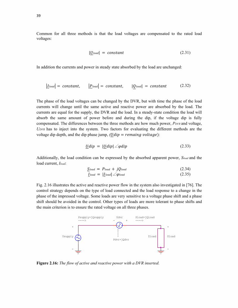
39
Common for all three methods is that the load voltages are compensated to the rated load voltages:
| | (2.31)
In addition the currents and power in steady state absorbed by the load are unchanged:
, , | | (2.32)
The phase of the load voltages can be changed by the DVR, but with time the phase of the load currents will change until the same active and reactive power are absorbed by the load. The currents are equal for the supply, the DVR and the load. In a steady-state condition the load will absorb the same amount of power before and during the dip, if the voltage dip is fully compensated. The differences between the three methods are how much power, PDVR and voltage, UDVR has to inject into the system. Two factors for evaluating the different methods are the voltage dip depth, and the dip phase jump, ( :
| |∠ (2.33)
Additionally, the load condition can be expressed by the absorbed apparent power, Sload and the load current, Iload: (2.34)
| |∠ (2.35) Fig. 2.16 illustrates the active and reactive power flow in the system also investigated in [76]. The control strategy depends on the type of load connected and the load response to a change in the phase of the impressed voltage. Some loads are very sensitive to a voltage phase shift and a phase shift should be avoided in the control. Other types of loads are more tolerant to phase shifts and the main criterion is to ensure the rated voltage on all three phases.
Figure 2.16: The flow of active and reactive power with a DVR inserted.
-
+ +
Uload
-
+-
Usupply
Psupply+jQsupply---->
Pload+jQload---->
Pdvr+jQdvr
---->
Zload
Udvr
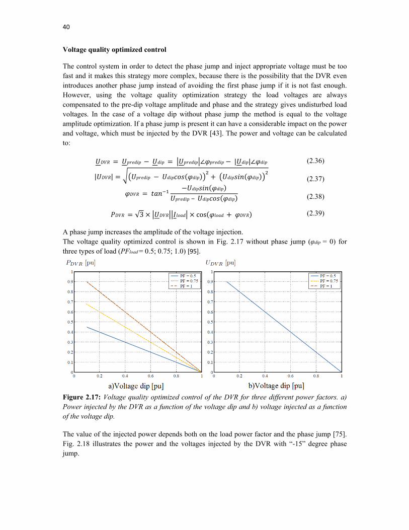
40
Voltage quality optimized control The control system in order to detect the phase jump and inject appropriate voltage must be too fast and it makes this strategy more complex, because there is the possibility that the DVR even introduces another phase jump instead of avoiding the first phase jump if it is not fast enough. However, using the voltage quality optimization strategy the load voltages are always compensated to the pre-dip voltage amplitude and phase and the strategy gives undisturbed load voltages. In the case of a voltage dip without phase jump the method is equal to the voltage amplitude optimization. If a phase jump is present it can have a considerable impact on the power and voltage, which must be injected by the DVR [43]. The power and voltage can be calculated to:
∠ | |∠ (2.36)
| | (2.37)
–
(2.38)
√3 cos (2.39)
A phase jump increases the amplitude of the voltage injection. The voltage quality optimized control is shown in Fig. 2.17 without phase jump (φdip = 0) for three types of load (PFload = 0.5; 0.75; 1.0) [95].
Figure 2.17: Voltage quality optimized control of the DVR for three different power factors. a) Power injected by the DVR as a function of the voltage dip and b) voltage injected as a function of the voltage dip. The value of the injected power depends both on the load power factor and the phase jump [75]. Fig. 2.18 illustrates the power and the voltages injected by the DVR with “-15” degree phase jump.
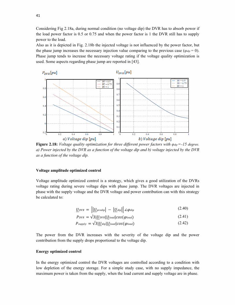
41
Considering Fig 2.18a, during normal condition (no voltage dip) the DVR has to absorb power if the load power factor is 0.5 or 0.75 and when the power factor is 1 the DVR still has to supply power to the load. Also as it is depicted in Fig. 2.18b the injected voltage is not influenced by the power factor, but the phase jump increases the necessary injection value comparing to the previous case (φdip = 0). Phase jump tends to increase the necessary voltage rating if the voltage quality optimization is used. Some aspects regarding phase jump are reported in [43].
Figure 2.18: Voltage quality optimization for three different power factors with φdip =-15 degree. a) Power injected by the DVR as a function of the voltage dip and b) voltage injected by the DVR as a function of the voltage dip. Voltage amplitude optimized control Voltage amplitude optimized control is a strategy, which gives a good utilization of the DVRs voltage rating during severe voltage dips with phase jump. The DVR voltages are injected in phase with the supply voltage and the DVR voltage and power contribution can with this strategy be calculated to:
∠ (2.40)
√3| || | (2.41)
√3| || | (2.42)
The power from the DVR increases with the severity of the voltage dip and the power contribution from the supply drops proportional to the voltage dip. Energy optimized control In the energy optimized control the DVR voltages are controlled according to a condition with low depletion of the energy storage. For a simple study case, with no supply impedance, the maximum power is taken from the supply, when the load current and supply voltage are in phase.
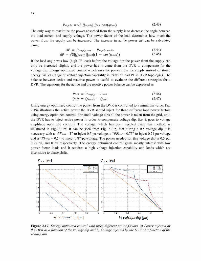
42
√3| || | (2.43)
The only way to maximize the power absorbed from the supply is to decrease the angle between the load current and supply voltage. The power factor of the load determines how much the power from the supply can be increased. The increase in active power ΔP can be calculated using:
, , (2.44) √3| || | 1 (2.45)
If the load angle was low (high PF load) before the voltage dip the power from the supply can only be increased slightly and the power has to come from the DVR to compensate for the voltage dip. Energy optimized control which uses the power from the supply instead of stored energy has less range of voltage injection capability in terms of load PF in DVR topologies. The balance between active and reactive power is useful to evaluate the different strategies for a DVR. The equations for the active and the reactive power balance can be expressed as:
(2.46) (2.47)
Using energy optimized control the power from the DVR is controlled to a minimum value. Fig. 2.19a illustrates the active power the DVR should inject for three different load power factors using energy optimized control. For small voltage dips all the power is taken from the grid, until the DVR has to inject active power in order to compensate voltage dip. (i.e. it goes to voltage amplitude optimized control). The voltage, which has been injected using this method, is illustrated in Fig. 2.19b. It can be seen from Fig. 2.19b, that during a 0.5 voltage dip it is necessary with a “PFload = 1” to inject 0.5 pu-voltage, a “PFload = 0.75” to inject 0.71 pu-voltage and a “PFload = 0.5” to inject 0.87 pu-voltage. The power needed for this voltage dip is 0.5 pu, 0.25 pu, and 0 pu respectively. The energy optimized control gains mostly interest with low power factor loads and it requires a high voltage injection capability and loads which are insensitive to phase shifts.
Figure 2.19: Energy optimized control with three different power factors. a) Power injected by the DVR as a function of the voltage dip and b) Voltage injected by the DVR as a function of the voltage dip.
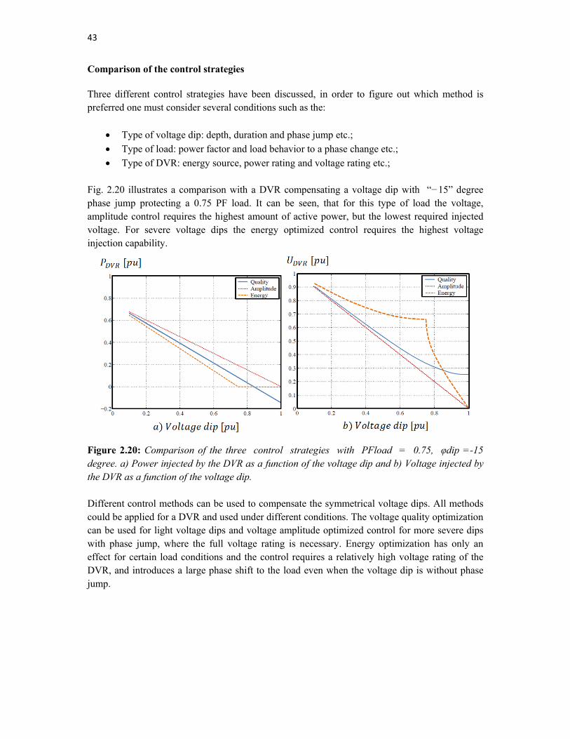
43
Comparison of the control strategies Three different control strategies have been discussed, in order to figure out which method is preferred one must consider several conditions such as the:
Type of voltage dip: depth, duration and phase jump etc.;
Type of load: power factor and load behavior to a phase change etc.;
Type of DVR: energy source, power rating and voltage rating etc.; Fig. 2.20 illustrates a comparison with a DVR compensating a voltage dip with “−15” degree phase jump protecting a 0.75 PF load. It can be seen, that for this type of load the voltage, amplitude control requires the highest amount of active power, but the lowest required injected voltage. For severe voltage dips the energy optimized control requires the highest voltage injection capability.
Figure 2.20: Comparison of the three control strategies with PFload = 0.75, φdip =-15 degree. a) Power injected by the DVR as a function of the voltage dip and b) Voltage injected by the DVR as a function of the voltage dip. Different control methods can be used to compensate the symmetrical voltage dips. All methods could be applied for a DVR and used under different conditions. The voltage quality optimization can be used for light voltage dips and voltage amplitude optimized control for more severe dips with phase jump, where the full voltage rating is necessary. Energy optimization has only an effect for certain load conditions and the control requires a relatively high voltage rating of the DVR, and introduces a large phase shift to the load even when the voltage dip is without phase jump.
44
2.6.2 Non-symmetrical voltage dips Even though compensation of non-symmetrical voltage dip is not among the aims of this thesis but it is worth to give a general review. A very large distribution of voltage dips recorded in a EPRI survey [42] are nonsymmetrical. In the survey approximately 87 % of the voltage dips were non-symmetrical. The distribution of voltage dips can vary with the system layout, the climate and the location. In the control it is important to distinguish between locations, in which the DVR should remove or ignore a sudden zero sequence voltage component from a non-symmetrical voltage dip. The control and analysis of zero sequence components in DVR system have been treated in [58]. Removing the zero sequence component complicates the control and measurement units. The DVR must be able to generate a zero sequence voltage and the control must be designed to handle a zero sequence component. If the DVR is located in an isolated MV grid there is not zero sequence component, but if it is located in the MV distribution system with an inductor grounded system or in LV distribution system, zero sequence voltage components can appear. Leaving the zero sequence aspects the focus is how to compensate positive and negative sequence components. The non-symmetry should be compensated to avoid tripping single-phase loads, two phase and three-phase loads. Therefore the DVR should compensate the positive sequence of the load voltage to rated value and suppress the negative sequence component in the supply voltage. A factor which can complicate the compensation of the negative sequence voltage is that the detection of a non-symmetrical fault is more difficult and the injection can be delayed because of time delay in the detection of a non-symmetrical voltage dip. Considering a symmetrical load the injection of a negative sequence voltage does not lead to a power drain of the energy storage and only a pulsating power flowing to and from the DC-link storage is expected.
2.7 Effect of load type The control strategy can be adapted to the load to avoid load tripping, and to have a maximum utilization of the DVR equipment. The DVR can introduce a number of unwanted effects such as transients, harmonics, non-symmetrical load voltages and phase shifts. The load voltage quality can generally be controlled, but often it is a tradeoff between the different parameters and also the load to be protected may have a certain characteristics, which favor some particular control strategies. The parameters, which can be controlled, are:
1- Phase shifts: the DVR can in theory compensate voltage dips with phase jump, but some of the disadvantages are more complex control system, difficult to implement, high voltage injections and power drain from the energy storage. Loads, which could be sensitive to phase shifts, are local generators, motors, and loads synchronized to the supply, such as supply commutated converters. Other loads may be robust to phase shifts, but it may lead to transients or in-rush currents in capacitors and transformers.
2- Restoration voltage level: the load voltages do not necessarily need to be restored to rated voltage. If the load tripping voltage is 0.7 pu voltage the load voltages can be restored to 0.75 pu;
45
3- Harmonics: the harmonics injected by the DVR can be controlled and filtered, but often at the expense of losses;
4- Over-voltage/under-voltage: a fast response is necessary for some loads and often at the expense of generating transients;
5- Transients: the DVR can lead to transients in the load voltages, especially in the transition phases in the beginning of a voltage dip and at the end of a voltage dip. Some loads may be sensitive to transients and the control should minimize the generation of transients;
In addition to the above mentioned parameters, the loads dependency of the voltage level has an impact on the stability of the control. The loads can be categorized according to:
Constant power;
Constant current;
Constant impedance;
The load voltage dependency is particular important if the DVR is not able to restore the load voltages. Then the absorbed current or power will change according to the type of load connected. The different types of load must be handled by the DVR and a robust performance is important. Assuming that injecting active power is necessary for voltage dip mitigation, if the load has a constant current or impedance behavior it can be worthwhile to restore the load voltages to as low voltages as necessary(less voltage injection capability is required). Thereby the load absorbs less power and the energy drain from the energy storage of DVR can be minimized. With a constant power load, the strategy does not give any benefits. Here, the current demanded by the load will increase and the risk of a current overload exists. With a constant power load it can even be considered to restore the load voltage to a higher voltage level to reduce the load current. The loads, which could be protected by the DVR, are here grouped and potential problems are described:
Time variable active/reactive power loads: large load voltage variations if the voltage drop across the DVR is not compensated;
Non-linear loads: a very large group of non-linear loads consists of single-phase and three-phase diode rectifies. Generally non-linear loads can lead to high load voltage distortion and initiating oscillations in the DVR line-filter;
Loads with bidirectional power flow: loads with reversed power flow require that the DVR storage can absorb power to be able to compensate for a voltage dip;
Non-symmetrical loads: can lead to non-symmetrical load voltages and power pulsations during compensation of symmetrical voltage dips;
Electrical machines: directly connected electrical machines can have high starting current and can be sensitive to voltage unbalance and phase shift. Electrical machines with a power electronic interface to the grid can have a completely different characteristic;
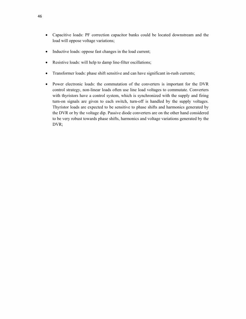
46
Capacitive loads: PF correction capacitor banks could be located downstream and the load will oppose voltage variations;
Inductive loads: oppose fast changes in the load current;
Resistive loads: will help to damp line-filter oscillations;
Transformer loads: phase shift sensitive and can have significant in-rush currents;
Power electronic loads: the commutation of the converters is important for the DVR control strategy, non-linear loads often use line load voltages to commutate. Converters with thyristors have a control system, which is synchronized with the supply and firing turn-on signals are given to each switch, turn-off is handled by the supply voltages. Thyristor loads are expected to be sensitive to phase shifts and harmonics generated by the DVR or by the voltage dip. Passive diode converters are on the other hand considered to be very robust towards phase shifts, harmonics and voltage variations generated by the DVR;
47
2.8 Simulation
In order to investigate the treated theories for implementing a DVR and observe its operation principle, a 3-phase distribution radial network of Fig. 2.21 with the parameters depicted in the table 2.4 is considered. Also based upon already presented procedures the DVR is designed for compensating the voltage dips with the voltage injection capability of 1 pu and using energy optimized strategy. The voltage controller is implemented through feedback voltage controller strategy.
Figure 2.21 Single-line diagram of a 3-phase radial LV-network equipped with the DVR.
Table 2.4 Parameters of LV distribution network of Fig. 2.21
The network was simulated in Matlab environment. The DVR control system was implemented based on energy optimized strategy. Thanks to this strategy the DVR real power exchange is almost zero (real power consumption will be limited to the losses within the VSC and the filter components). Therefore the DVR will restore the feeder voltage through exchange of only reactive power.
20 [kV]
=180 [kVA] , = 0.04% , =20[kV]/230[V]
_ =0.125+0.0742i [mΩ/m], Cable 185mm^2 1) , at load-bus 3 %
Length=250 [m]
3-phase star connection
=150 [kVA] =230[V] 0.85 lagging
3 ∗ 50 , 0.04% , 230 /230
0.5 1
75 500
20

48
At first a symmetrical voltage dip is applied to the grid voltage during the time interval of 0.4 to 0.6 in such a way that the remaining voltage is 0.875 [pu]. As it can be seen from Fig. 2.22 the DVR restores the load voltage successfully in such a way that the load almost does not see any voltage disturbance.
Figure 2.22 Performance of the DVR during voltage dip. a)The grid voltage b) The DVR voltage c) The load voltage
Thereafter in order to investigate the performance of the employed strategy, another type of symmetrical voltage disturbance is considered. During the time interval of 0.4 to 0.6 a symmetrical voltage swell is applied to the grid voltage so that the voltage of M-bus becomes 1.125 [pu]. As it is represented in the Fig. 2.23 the DVR compensates the voltage swell successfully so that the load voltage remains almost constant.
Figure 2.23 Performance of the DVR during voltage swell. a)The grid voltage b) The DVR voltage c) The load voltage
49
2.9 Summary
The location of the DVR and the differences in placing the DVR at the medium voltage distribution system or at the low voltage distribution system has been discussed.Thereafter DVR topologies including the connection of converter with or without an injection transformer, converter topologies and how to obtain the active power necessary to compensate some voltage dips have been analyzed. Some of the main conclusions are:
The placement of a large DVR at the medium voltage level can simplify the DVR topology and minimize the losses and voltage drop across the DVR;
A DVR topology using an injection transformer is expected to give certain benefits regarding the converter topology, the charging circuit and the protection of the DVR;
Regarding the converter topology one of the first aspects is the capability of the topology to inject zero sequence voltages in order to compensate non-symmetrical voltage dips. A higher number of synthesized voltage levels can be beneficial in order to reduce the size of the line-filter;
In a strong grid and with a rare intensity of severe voltage dips, DVR topologies without any significant energy storage can be an interesting alternative. A shunt converter at the load side of the series converter can have a good performance, but at the expense of a high installed converter capacity;
DVR limitations have been treated, which could influence the control strategy. Different operation modes have been described for a DVR including standby mode, active mode and bypass mode, which have been incorporated in the control system;
Different control strategies have been treated, such as voltage quality optimized control, voltage amplitude optimized control and energy optimized control. The control methods have been discussed with respect to voltage quality, voltage injection, power drain of the energy storage and how it may the influence the connected load;
The effects of load types (which are supposed to be protected) on the control strategies and the voltage drop across the DVR are described;

50
CHAPTER 3
Implementing fault current limiting function
3.1 Incentives
As already discussed in the previous chapter the DVR is designed to improve quality of voltage at medium voltage or low voltage level distribution system. The primary function of the DVR is to protect downstream sensitive consumers from effects of upstream voltage disturbance including voltage sags and swells. Unfortunately faults do occur on the distribution system downstream of the DVR. Considering the Fig 3.1 the faulted point could be anywhere on the feeder connecting the DVR and the protected load. Owing to the fact that DVR is series connected to the faulted feeder, a large current will pass through the injection transformer and into the DVR converter. Generally the main power network is designed and sized for withstanding against such short circuit transient current before the operation of the circuit breaker. But limiting such transient short circuit current is demanded from some points of view. In fact without proper considerations, the high short circuit current could easily damage the injection transformer, destroy insulators and more important break power electronic switches which are more sensitive to high current. In order to break the fault current, one can of course rely on the circuit breakers installed upstream of the DVR. Depending on algorithm of protection coordination and the exact location/nature of the fault, the fault clearing action may typically take some cycles. However, fault current during these cycles can still have damaging effect on the power switching devices within the DVR. Moreover, for the other parallel loads the voltage sag event due to fault current can be harmful as it can cause equipment on these parallel feeders to fail, malfunction, or shut down. In addition, at the moment of fault occurrence if the DVR is not controlled properly, the DVR might also contribute to the PCC voltage sag in the process of compensating the missing voltage, thus it further worsens the fault situation.
Figure 3.1: A typical configuration of radial LV distribution network equipped with the DVR
Considering these issues together with the cost of installed equipment, it proves the necessity of employing appropriate strategy in order to limit the downstream fault current.
51
3.2 Network fault analysis
3.2.1 Necessity of fault analysis Short-circuit fault analysis is carried out to ensure the safety of systems, workers as well as the general public. Power system equipment such as circuit breakers can fail catastrophically if they are subjected to fault duties that exceed their rating. Other equipment such as bus-bars, transformers and cables can fail thermally or mechanically if subjected to fault currents in excess of ratings. Other areas where fault analysis is carried out are for the calculation of induced voltages on adjacent communication circuits, pipelines, fences and other metallic objects. Short circuit current calculations are made at the system design stage to determine the short circuit ratings of new switchgear and substation infrastructure equipment to be provided and installed. Switchgear manufacturers design their circuit breakers to ensure that they are capable of making, breaking and carrying the specified short circuit current for a short time. System reinforcements may be triggered by network expansion and/or the connection of new generating plant to the power system. Routine calculations are also made to check the continued adequacy of existing equipment as system operating configurations are modified. In addition, evaluation of minimum short circuit currents are made and used in the calculation of protection relay settings to ensure accurate and coordinated relay operations. Maximum short circuit current calculations are carried out for sizing and designing the substations and grid. Short circuit analysis is also carried out as a part of initial power quality assessments for the connection of disturbing loads to electrical power networks. These assessments include voltage flicker, harmonic analysis and voltage unbalance. Other area where short circuit analysis is carried out is in the modification of an existing system such as installing a new auxiliary electrical power system including DVRs. Equipment with standardized short circuit ratings are designed and produced by manufacturers. Also, manufacturers of substation infrastructure equipment and other power system plant, e.g. transformers and cables, use the short circuit current ratings specified by their customers to ensure that the equipment is designed to safely withstand the passage of these currents for the duration specified. Short circuit faults can occur between phases, or between phases and earth, or both. Short circuits may be one-phase to earth, phase to phase, two-phase to earth, three-phase clear of earth and three-phase to earth. The three-phase fault that symmetrically affects the three phases of a three-phase circuit is the only balanced fault whereas all the other faults are unbalanced. The vast majority of short circuit faults are weather related followed by equipment failure. The weather factors that usually cause short-circuit faults are: lightning strikes, accumulation of snow or ice, heavy rain, strong winds or gales, salt pollution depositing on insulators on overhead lines and in substations, floods and fires adjacent to electrical equipment. Equipment failure, e.g. machines, transformers, reactors, cables and etc., cause many short circuit faults. These may be due to failure of internal insulation because of ageing and degradation. Short circuit faults may also be caused by human error. A classic example is one where maintenance staffs inadvertently leave isolated equipment connected through safety earth clamps when maintenance work is completed.
3.2.2 Short circuit current waveform The initial magnitude of the dc current component in any phase depends on the instant of the voltage waveform when the short circuit occurs, and on the magnitude of the ac current component. The rate of decay of the dc current component in the three phases depends on the circuit time constant L/R or
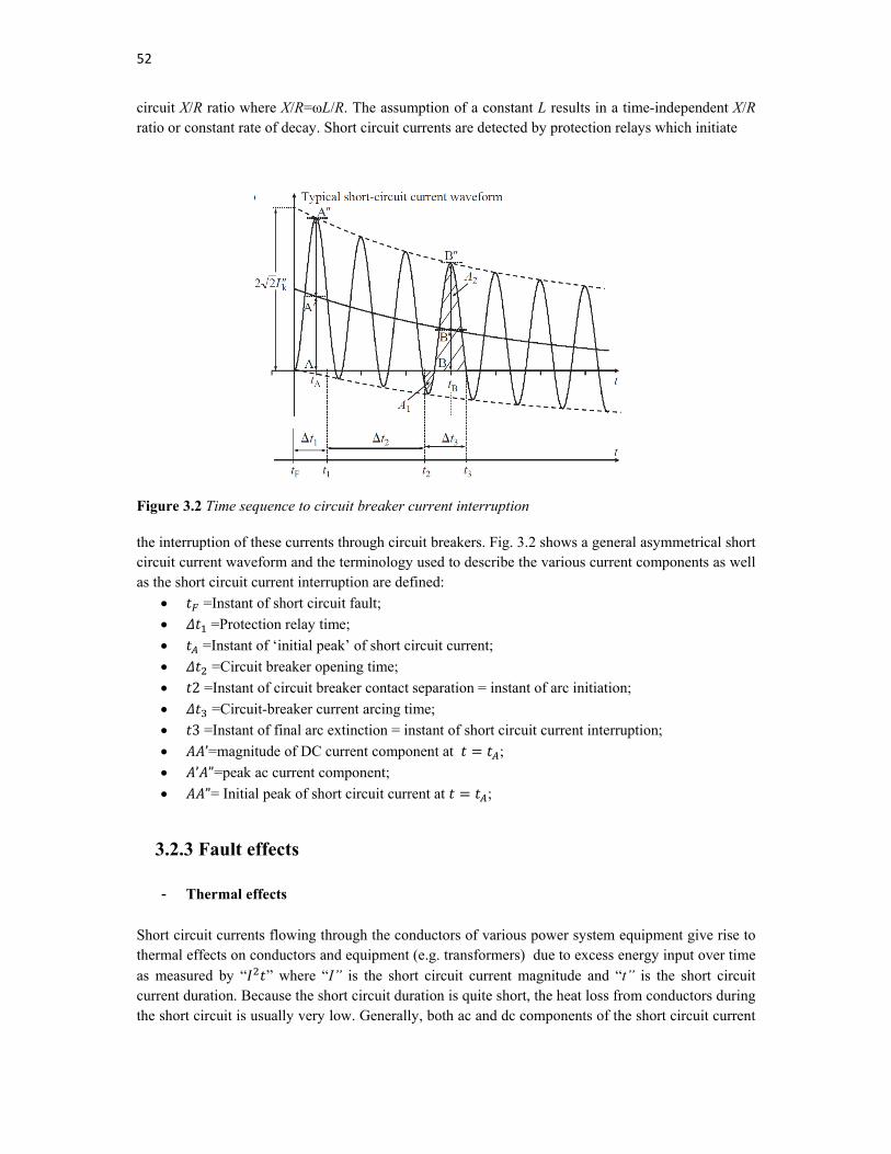
52
circuit X/R ratio where X/R=ωL/R. The assumption of a constant L results in a time-independent X/R ratio or constant rate of decay. Short circuit currents are detected by protection relays which initiate
Figure 3.2 Time sequence to circuit breaker current interruption the interruption of these currents through circuit breakers. Fig. 3.2 shows a general asymmetrical short circuit current waveform and the terminology used to describe the various current components as well as the short circuit current interruption are defined:
=Instant of short circuit fault;
=Protection relay time;
=Instant of ‘initial peak’ of short circuit current;
=Circuit breaker opening time;
2 =Instant of circuit breaker contact separation = instant of arc initiation;
=Circuit-breaker current arcing time;
3 =Instant of final arc extinction = instant of short circuit current interruption;
’=magnitude of DC current component at ;
’ ”=peak ac current component;
”= Initial peak of short circuit current at ;
3.2.3 Fault effects
- Thermal effects Short circuit currents flowing through the conductors of various power system equipment give rise to thermal effects on conductors and equipment (e.g. transformers) due to excess energy input over time as measured by “ ” where “I” is the short circuit current magnitude and “t” is the short circuit current duration. Because the short circuit duration is quite short, the heat loss from conductors during the short circuit is usually very low. Generally, both ac and dc components of the short circuit current
53
contribute to the thermal heating of conductors. The three-phase short circuit fault normally results in the highest thermal effect on equipment.
- Mechanical effects
Short circuit currents flowing through the conductors of various power system equipment create electromagnetic forces and mechanical stresses on equipment such as overhead line conductors, bus-bars and their supports, cables and transformer windings. Mechanical forces on transformer windings are both radial and axial. The transformer windings must be designed to withstand the mechanical forces created by the short circuit currents. In modern power systems, there are various types of active sources that can contribute short circuit currents in the event of short circuit faults on the power system. These include synchronous and induction generators, synchronous and induction motors and modern power electronics converter connected generators. Power system elements such as lines, cables, transformers and series reactors between the short circuit fault location and the various current sources will affect the magnitude of the short circuit currents infeed into the fault. The effect is generally to reduce the magnitude of the short circuit currents and to increase the rate at which the dc components will decay. In design/modification stage it is necessary to calculate the ac and dc components of the short circuit current at the fault location in systems that generally contain many different sources.
3.2.4 Short circuit current terminology and definitions Standards ER G7/4 and IEC 60909 give calculation strategies for short circuits current. In IEC 60947-2 , IEC 60898-1 and ANSI C37.13 the standard definitions and terminology for short circuit, circuit breakers and fuses are treated.
- Prospective short circuit current: the highest current which is likely to flow in a circuit if line and neutral cables are short circuited is called the prospective short circuit current (PSC). It is the largest current which can flow in the system and protective devices must be capable of breaking it safely. The breaking capacity of a fuse or of a circuit breaker is one of the factors which needs to be considered in its selection, but before using other equipment the installer must make sure that their breaking capacity exceeds the PSC at the point which they are supposed to be installed; The effective breaking capacity of overcurrent devices varies widely with their construction. For instance semi-enclosed fuses are capable of breaking currents of 1 kA to 4 kA depending on their type while cartridge fuses (BS1361 type) will safely break at 16.5 kA for type 1 or 33 kA for type II. Prospective short circuit current is driven by the e.m.f. of the supply through impedance made up of transformer windings and the cables from the supply to the fault. The impedance of the cables will depend on their size and length, so the PSC value will vary throughout the installation, becoming smaller as the distance from the intake position increases;
- (let through energy): an expression related to the circuit energy as a result of current flow. Referring to circuit breakers, the [A2S] is expressed for the current flow between the initiation of the fault current and the clearing time;
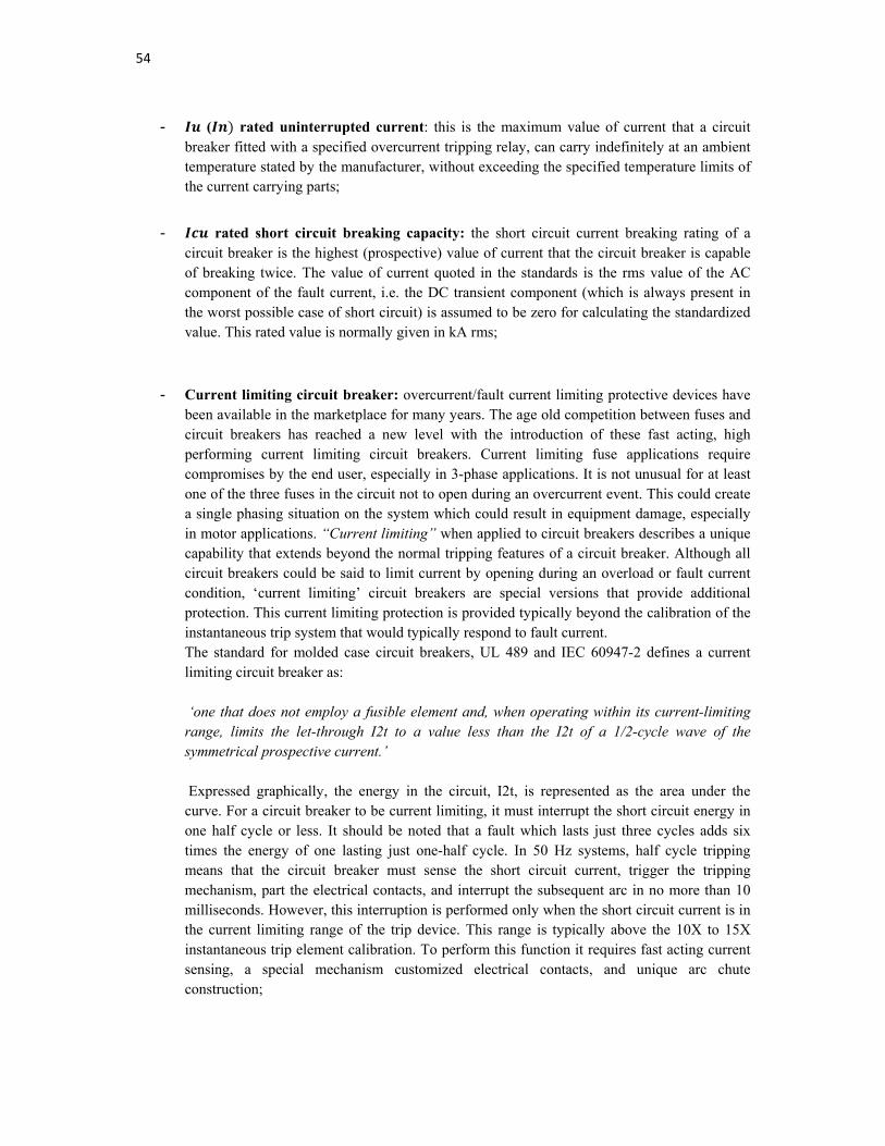
54
- ( rated uninterrupted current: this is the maximum value of current that a circuit
breaker fitted with a specified overcurrent tripping relay, can carry indefinitely at an ambient temperature stated by the manufacturer, without exceeding the specified temperature limits of the current carrying parts;
- rated short circuit breaking capacity: the short circuit current breaking rating of a circuit breaker is the highest (prospective) value of current that the circuit breaker is capable of breaking twice. The value of current quoted in the standards is the rms value of the AC component of the fault current, i.e. the DC transient component (which is always present in the worst possible case of short circuit) is assumed to be zero for calculating the standardized value. This rated value is normally given in kA rms;
- Current limiting circuit breaker: overcurrent/fault current limiting protective devices have been available in the marketplace for many years. The age old competition between fuses and circuit breakers has reached a new level with the introduction of these fast acting, high performing current limiting circuit breakers. Current limiting fuse applications require compromises by the end user, especially in 3-phase applications. It is not unusual for at least one of the three fuses in the circuit not to open during an overcurrent event. This could create a single phasing situation on the system which could result in equipment damage, especially in motor applications. “Current limiting” when applied to circuit breakers describes a unique capability that extends beyond the normal tripping features of a circuit breaker. Although all circuit breakers could be said to limit current by opening during an overload or fault current condition, ‘current limiting’ circuit breakers are special versions that provide additional protection. This current limiting protection is provided typically beyond the calibration of the instantaneous trip system that would typically respond to fault current. The standard for molded case circuit breakers, UL 489 and IEC 60947-2 defines a current limiting circuit breaker as: ‘one that does not employ a fusible element and, when operating within its current-limiting range, limits the let-through I2t to a value less than the I2t of a 1/2-cycle wave of the symmetrical prospective current.’ Expressed graphically, the energy in the circuit, I2t, is represented as the area under the curve. For a circuit breaker to be current limiting, it must interrupt the short circuit energy in one half cycle or less. It should be noted that a fault which lasts just three cycles adds six times the energy of one lasting just one-half cycle. In 50 Hz systems, half cycle tripping means that the circuit breaker must sense the short circuit current, trigger the tripping mechanism, part the electrical contacts, and interrupt the subsequent arc in no more than 10 milliseconds. However, this interruption is performed only when the short circuit current is in the current limiting range of the trip device. This range is typically above the 10X to 15X instantaneous trip element calibration. To perform this function it requires fast acting current sensing, a special mechanism customized electrical contacts, and unique arc chute construction;
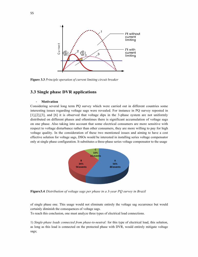
55
Figure 3.3 Principle operation of current limiting circuit breaker
3.3 Single phase DVR applications
- Motivation Considering several long term PQ survey which were carried out in different countries some interesting issues regarding voltage sags were revealed. For instance in PQ survey reposted in [1],[2],[3], and [6] it is observed that voltage dips in the 3-phase system are not uniformly distributed on different phases and oftentimes there is significant accumulation of voltage sags on one phase. Also taking into account that some electrical consumers are more sensitive with respect to voltage disturbance rather than other consumers, they are more willing to pay for high voltage quality. In the consideration of these two mentioned issues and aiming to have a cost effective solution for voltage sags, DSOs would be interested in installing series voltage compensator only at single phase configuration. It substitutes a three-phase series voltage compensator to the usage
Figure3.4 Distribution of voltage sags per phase in a 3-year PQ survey in Brazil of single phase one. This usage would not eliminate entirely the voltage sag occurrence but would certainly diminish the consequences of voltage sags. To reach this conclusion, one must analyze three types of electrical load connections. 1) Single-phase loads connected from phase-to-neutral: for this type of electrical load, this solution, as long as this load is connected on the protected phase with DVR, would entirely mitigate voltage sags;
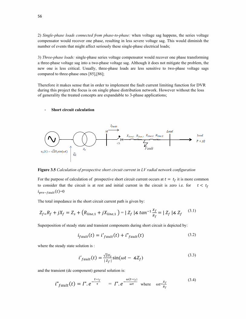
56
2) Single-phase loads connected from phase-to-phase: when voltage sag happens, the series voltage compensator would recover one phase, resulting in less severe voltage sag. This would diminish the number of events that might affect seriously these single-phase electrical loads; 3) Three-phase loads: single-phase series voltage compensator would recover one phase transforming a three-phase voltage sag into a two-phase voltage sag. Although it does not mitigate the problem, the new one is less critical. Usually, three-phase loads are less sensitive to two-phase voltage sags compared to three-phase ones [85],[86]; Therefore it makes sense that in order to implement the fault current limiting function for DVR during this project the focus is on single phase distribution network. However without the loss of generality the treated concepts are expandable to 3-phase applications;
- Short circuit calculation
Figure 3.5 Calculation of prospective short circuit current in LV radial network configuration
For the purpose of calculation of prospective short circuit current occurs at it is more common
to consider that the circuit is at rest and initial current in the circuit is zero i.e. for
=0
The total impedance in the short circuit current path is given by:
, , = | |∡ | |∡
(3.1)
Superposition of steady state and transient components during short circuit is depicted by:
"
(3.2)
where the steady state solution is :
√| |
sin ∡ )
(3.3)
and the transient (dc component) general solution is:
" ". = ". where ωτ= (3.4)
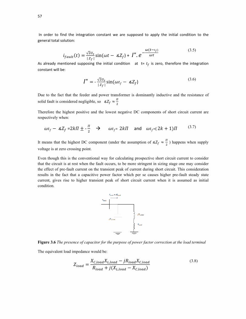
57
In order to find the integration constant we are supposed to apply the initial condition to the
general total solution:
√
| |sin ∡ ) + ".
(3.5)
As already mentioned supposing the initial condition at t= is zero, therefore the integration
constant will be:
" ‐ √
| |sin ∡ )
(3.6)
Due to the fact that the feeder and power transformer is dominantly inductive and the resistance of
solid fault is considered negligible, so ∡
Therefore the highest positive and the lowest negative DC components of short circuit current are respectively when:
∡ =2 ‐ = 2 and =( 2 1
(3.7)
It means that the highest DC component (under the assumption of ∡ ) happens when supply
voltage is at zero crossing point.
Even though this is the conventional way for calculating prospective short circuit current to consider that the circuit is at rest when the fault occurs, to be more stringent in sizing stage one may consider the effect of pre-fault current on the transient peak of current during short circuit. This consideration results in the fact that a capacitive power factor which per se causes higher pre-fault steady state current, gives rise to higher transient peak of short circuit current when it is assumed as initial condition.
Figure 3.6 The presence of capacitor for the purpose of power factor correction at the load terminal
The equivalent load impedance would be:
, , ,
, ,
(3.8)
58
And the steady state pre-fault current is:
√
| |sin ∡ ) = √2 sin ∡ )
(3.9)
It is a trivial conclusion that increasing gives rise to smaller which causes higher " ".
However the power factor correction capacitor installed at the load terminal does not make the load current capacitive and in the best performance it gives unit power factor. Also due to short length of secondary distribution feeders we may say that capacitive power factor (leading PF) in LV network is a rare issue, therefore in order to consider the initial condition and integrate the effect of steady state pre-fault current in the calculation of transient peak of short circuit current to find the highest peak it is enough to consider the unit power factor load as the worst case in LV grid.
In order to implement FCL function in a DVR throughout this chapter we need an indicator to compare the effectiveness of each proposed solutions. Let`s calculate the prospective short circuit current in the typical radial LV network of Fig 3.5 before the installation of DVR and with the parameters depicted in table 3.1 :
Table 3.1: Parameters of the specified LV distribution network of Fig. 3.5
High index for the peak of short circuit current
- Fault occurs at the M-bus; - Fault instance is the moment which results in the highest possible DC component; - Pre-fault current is the grid rated current with unit power factor;
Low index for the peak of short circuit current
- Fault occurs at the load-bus; - Fault instance is the moment which results in zero DC component which means no transient
behavior in short circuit current waveform;
The simulation result in Matlab environment for “high index” and “low index” for short circuit current in this chapter with the parameter depicted in table 3.1 gives the following curves in Fig. 3.7 and 3.8 respectively.
20 [kV]
=60 [kVA] , = 0.04% , =20[kV]/230[V]
=0.125+0.0742i [mΩ/m], Cable 185mm^2 at load-bus= 3%)
250 ]
=50 [kVA] =230[V] 1
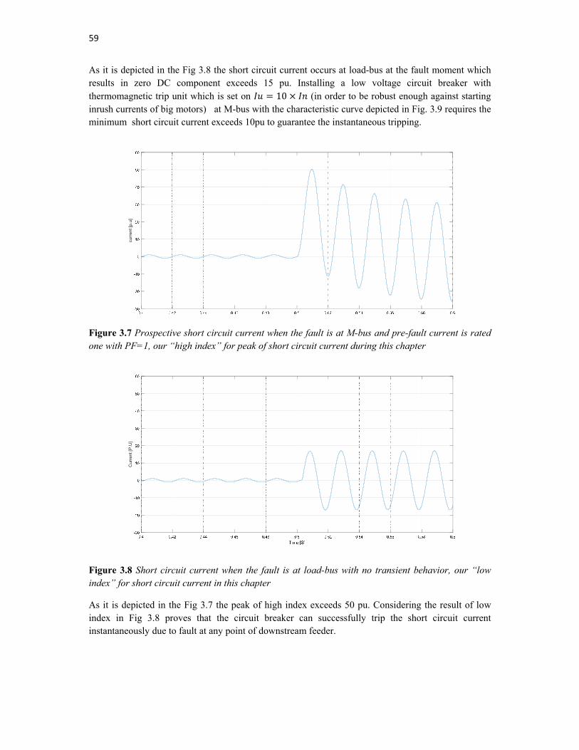
59
As it is depicted in the Fig 3.8 the short circuit current occurs at load-bus at the fault moment which results in zero DC component exceeds 15 pu. Installing a low voltage circuit breaker with thermomagnetic trip unit which is set on 10 (in order to be robust enough against starting inrush currents of big motors) at M-bus with the characteristic curve depicted in Fig. 3.9 requires the minimum short circuit current exceeds 10pu to guarantee the instantaneous tripping.
Figure 3.7 Prospective short circuit current when the fault is at M-bus and pre-fault current is rated one with PF=1, our “high index” for peak of short circuit current during this chapter
Figure 3.8 Short circuit current when the fault is at load-bus with no transient behavior, our “low index” for short circuit current in this chapter
As it is depicted in the Fig 3.7 the peak of high index exceeds 50 pu. Considering the result of low index in Fig 3.8 proves that the circuit breaker can successfully trip the short circuit current instantaneously due to fault at any point of downstream feeder.
curr
ent [
p.u]
Cur
rent
[P.U
]
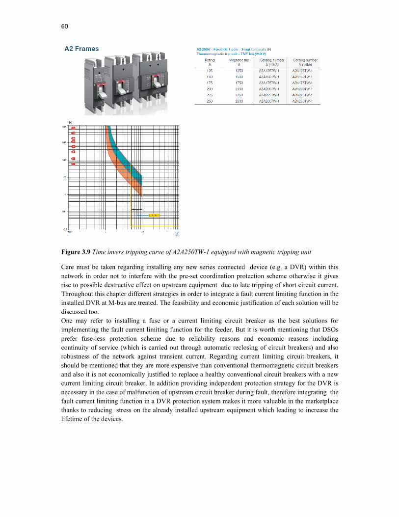
60
Figure 3.9 Time invers tripping curve of A2A250TW-1 equipped with magnetic tripping unit
Care must be taken regarding installing any new series connected device (e.g. a DVR) within this network in order not to interfere with the pre-set coordination protection scheme otherwise it gives rise to possible destructive effect on upstream equipment due to late tripping of short circuit current. Throughout this chapter different strategies in order to integrate a fault current limiting function in the installed DVR at M-bus are treated. The feasibility and economic justification of each solution will be discussed too. One may refer to installing a fuse or a current limiting circuit breaker as the best solutions for implementing the fault current limiting function for the feeder. But it is worth mentioning that DSOs prefer fuse-less protection scheme due to reliability reasons and economic reasons including continuity of service (which is carried out through automatic reclosing of circuit breakers) and also robustness of the network against transient current. Regarding current limiting circuit breakers, it should be mentioned that they are more expensive than conventional thermomagnetic circuit breakers and also it is not economically justified to replace a healthy conventional circuit breakers with a new current limiting circuit breaker. In addition providing independent protection strategy for the DVR is necessary in the case of malfunction of upstream circuit breaker during fault, therefore integrating the fault current limiting function in a DVR protection system makes it more valuable in the marketplace thanks to reducing stress on the already installed upstream equipment which leading to increase the lifetime of the devices.
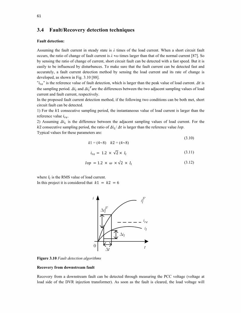
61
3.4 Fault/Recovery detection techniques Fault detection:
Assuming the fault current in steady state is λ times of the load current. When a short circuit fault occurs, the ratio of change of fault current is λ ∗ω times larger than that of the normal current [87]. So by sensing the ratio of change of current, short circuit fault can be detected with a fast speed. But it is easily to be influenced by disturbances. To make sure that the fault current can be detected fast and accurately, a fault current detection method by sensing the load current and its rate of change is developed, as shown in Fig. 3.10 [88]. " " is the reference value of fault detection, which is larger than the peak value of load current. is
the sampling period. and are the differences between the two adjacent sampling values of load current and fault current, respectively. In the proposed fault current detection method, if the following two conditions can be both met, short circuit fault can be detected. 1) For the 1 consecutive sampling period, the instantaneous value of load current is larger than the reference value . 2) Assuming is the difference between the adjacent sampling values of load current. For the 2consecutive sampling period, the ratio of / is larger than the reference value .
Typical values for these parameters are:
k1 = (4∼8) 2 = (4∼8)
(3.10)
1.2 √2
(3.11)
1.2 √2
(3.12)
where is the RMS value of load current. In this project it is considered that 1 2 6
Figure 3.10 Fault detection algorithms
Recovery from downstream fault
Recovery from a downstream fault can be detected through measuring the PCC voltage (voltage at load side of the DVR injection transformer). As soon as the fault is cleared, the load voltage will
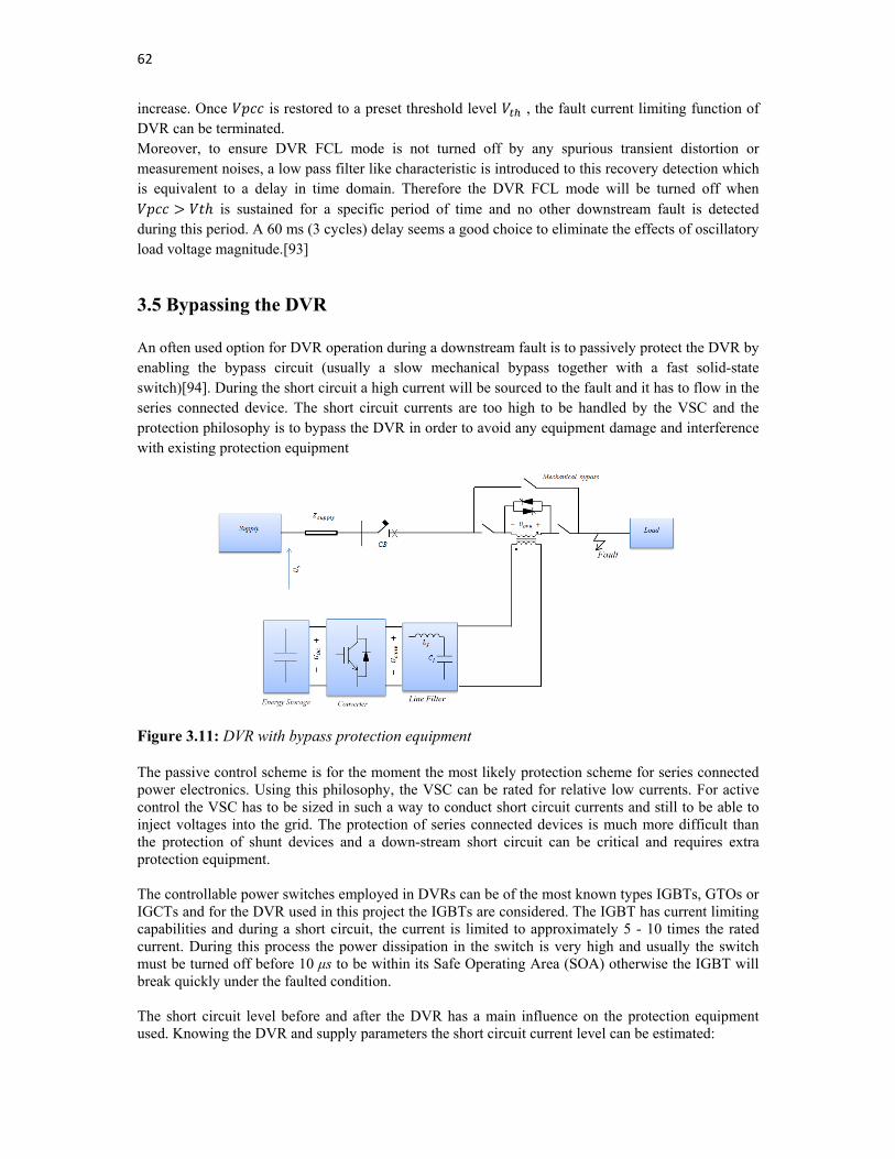
62
increase. Once is restored to a preset threshold level , the fault current limiting function of DVR can be terminated. Moreover, to ensure DVR FCL mode is not turned off by any spurious transient distortion or measurement noises, a low pass filter like characteristic is introduced to this recovery detection which is equivalent to a delay in time domain. Therefore the DVR FCL mode will be turned off when
is sustained for a specific period of time and no other downstream fault is detected during this period. A 60 ms (3 cycles) delay seems a good choice to eliminate the effects of oscillatory load voltage magnitude.[93]
3.5 Bypassing the DVR An often used option for DVR operation during a downstream fault is to passively protect the DVR by enabling the bypass circuit (usually a slow mechanical bypass together with a fast solid-state switch)[94]. During the short circuit a high current will be sourced to the fault and it has to flow in the series connected device. The short circuit currents are too high to be handled by the VSC and the protection philosophy is to bypass the DVR in order to avoid any equipment damage and interference with existing protection equipment
Figure 3.11: DVR with bypass protection equipment The passive control scheme is for the moment the most likely protection scheme for series connected power electronics. Using this philosophy, the VSC can be rated for relative low currents. For active control the VSC has to be sized in such a way to conduct short circuit currents and still to be able to inject voltages into the grid. The protection of series connected devices is much more difficult than the protection of shunt devices and a down-stream short circuit can be critical and requires extra protection equipment. The controllable power switches employed in DVRs can be of the most known types IGBTs, GTOs or IGCTs and for the DVR used in this project the IGBTs are considered. The IGBT has current limiting capabilities and during a short circuit, the current is limited to approximately 5 - 10 times the rated current. During this process the power dissipation in the switch is very high and usually the switch must be turned off before 10 μs to be within its Safe Operating Area (SOA) otherwise the IGBT will break quickly under the faulted condition. The short circuit level before and after the DVR has a main influence on the protection equipment used. Knowing the DVR and supply parameters the short circuit current level can be estimated:
63
, (3.13)
| |
| |
(3.14)
where , is the pu value of total voltage drop across the DVR. Assuming , 0.04pu,
0.04pu the steady state short circuit current can with this very simple example be calculated to more than 12 times the rated current, however apart from the steady state value of short circuit current, the main problem is caused by very higher value of short circuit current during transient interval which even exceeds 50 pu. Ideally, the converter should conduct the current until the protection equipment has cleared the fault, but it would require significantly more powerful IGBT to withstand such a high current for the required fault clearing time e.g. 5 to 10 cycles. Turning the power switches off makes only a current path through the diodes when the voltage across the DVR is larger than the DC-link voltage level. Therefore, turning off the power switches will lead to an uncontrolled charging of the DC-link capacitor. The uncontrolled charging can in some DVR design cause a destructive DC-voltage level, which will damage the power modules and the DC capacitors. The highest risk of damage will arise if the rated DC-link voltage is close to the maximum allowable DC-voltage. The first protection scheme for the DVR could be achieved with thyristors and mechanical bypass. In several DVR protection schemes thyristors are intended to take over the current for the VSC until a more robust and slower mechanically bypass is ensured. The method to ensure a current path is explained in the following way.
As soon as fault is detected the zero-state condition (no switching commande) is applied to the converter. The current can be still flowing through the diodes. Appropriate sizing is required for the diodes in order to withstand against this high current before the bypass is successfully achieved. At the same time the on-state is applied to the anti-parallel thyristors placed at the primary side of transformer. Thyristors can react fast and bypass the DVR. Thereafter the mechanical bypass switch is closed. Mechanical bypass protection is relative slow, but robust, cheap and easy to control.
A DVR with the characteristic parameters depicted in table 3.2 was inserted to the same pre-defined LV network of Fig. 3.5. The results of implementing this strategy in Matlab environment are treated in the following figures.
Injection Transformer , . % , /
Bypass thyristor
1_ 0.8_ 2 _ 250
DVR LC filter 0.5 1DC-link storage 75 500
Table 3.2 DVR characteristic parameters
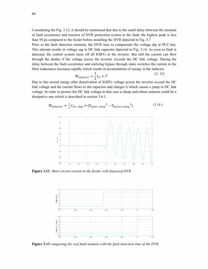
64
Considering the Fig. 3.12, it should be mentioned that due to the small delay between the moment of fault occurrence and reaction of DVR protection system to the fault, the highest peak is less than 50 pu compared to the feeder before installing the DVR depicted in Fig. 3.7 Prior to the fault detection moment, the DVR tries to compensate the voltage dip at PCC-bus. This attempt results in voltage sag in DC link capacitor depicted in Fig. 3.14. As soon as fault is detected, the control system turns off all IGBTs in the inverter. But still the current can flow through the diodes if the voltage across the inverter exceeds the DC link voltage. During the delay between the fault occurrence and realizing bypass through static switches the current in the filter inductance increases rapidly which results in accumulation of energy in the inductor.
12
(3. 15)
Due to this stored energy after deactivation of IGBTs voltage across the inverter exceed the DC link voltage and the current flows to the capacitor and charges it which causes a jump in DC link voltage. In order to protect the DC link voltage in that case a cheap and robust solution could be a dissipative one which is described in section 3.6.1.
(3.16 )
Figure 3.12 Short circuit current in the feeder with bypassed DVR
Figure 3.13 comparing the real fault moment with the fault detection time of the DVR
0.4 0.42 0.44 0.46 0.48 0.5 0.52 0.54 0.56 0.58 0.6-30
-20
-10
0
10
20
30
40
50
0.49 0.492 0.494 0.496 0.498 0.5 0.502-0.2
0
0.2
0.4
0.6
0.8
1
1.2
0.49 0.492 0.494 0.496 0.498 0.5 0.502-0.2
0
0.2
0.4
0.6
0.8
1
1.2
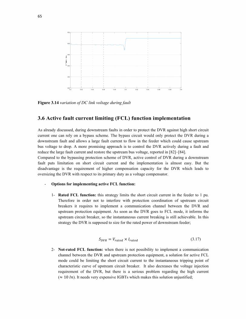
65
Figure 3.14 variation of DC link voltage during fault
3.6 Active fault current limiting (FCL) function implementation As already discussed, during downstream faults in order to protect the DVR against high short circuit current one can rely on a bypass scheme. The bypass circuit would only protect the DVR during a downstream fault and allows a large fault current to flow in the feeder which could cause upstream bus voltage to drop. A more promising approach is to control the DVR actively during a fault and reduce the large fault current and restore the upstream bus voltage, reported in [82]–[84]. Compared to the bypassing protection scheme of DVR, active control of DVR during a downstream fault puts limitation on short circuit current and the implementation is almost easy. But the disadvantage is the requirement of higher compensation capacity for the DVR which leads to oversizing the DVR with respect to its primary duty as a voltage compensator.
- Options for implementing active FCL function: 1- Rated FCL function: this strategy limits the short circuit current in the feeder to 1 pu.
Therefore in order not to interfere with protection coordination of upstream circuit breakers it requires to implement a communication channel between the DVR and upstream protection equipment. As soon as the DVR goes to FCL mode, it informs the upstream circuit breaker, so the instantaneous current breaking is still achievable. In this strategy the DVR is supposed to size for the rated power of downstream feeder;
(3.17)
2- Not-rated FCL function: when there is not possibility to implement a communication
channel between the DVR and upstream protection equipment, a solution for active FCL mode could be limiting the short circuit current to the instantaneous tripping point of characteristic curve of upstream circuit breaker. It also decreases the voltage injection requirement of the DVR, but there is a serious problem regarding the high current ( 10 ). It needs very expensive IGBTs which makes this solution unjustified;
0.4 0.42 0.44 0.46 0.48 0.5 0.52 0.54 0.56 0.58 0.6300
350
400
450
500
550
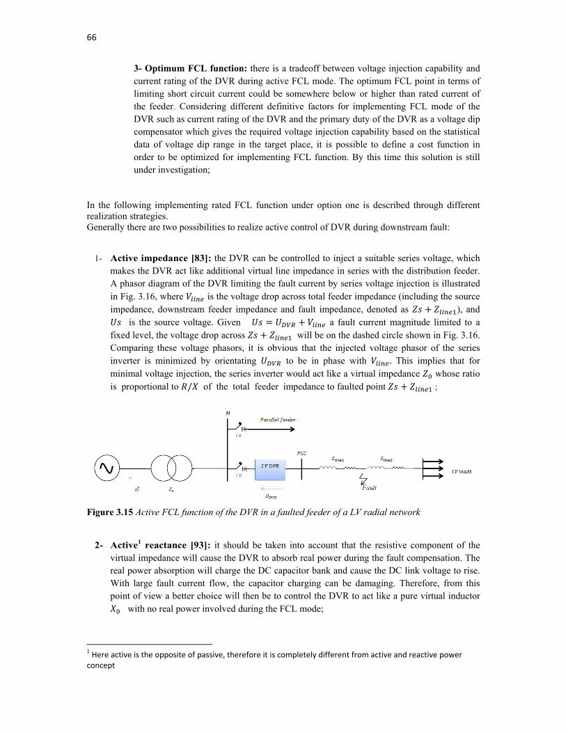
66
3- Optimum FCL function: there is a tradeoff between voltage injection capability and current rating of the DVR during active FCL mode. The optimum FCL point in terms of limiting short circuit current could be somewhere below or higher than rated current of the feeder. Considering different definitive factors for implementing FCL mode of the DVR such as current rating of the DVR and the primary duty of the DVR as a voltage dip compensator which gives the required voltage injection capability based on the statistical data of voltage dip range in the target place, it is possible to define a cost function in order to be optimized for implementing FCL function. By this time this solution is still under investigation;
In the following implementing rated FCL function under option one is described through different realization strategies. Generally there are two possibilities to realize active control of DVR during downstream fault:
1- Active impedance [83]: the DVR can be controlled to inject a suitable series voltage, which makes the DVR act like additional virtual line impedance in series with the distribution feeder. A phasor diagram of the DVR limiting the fault current by series voltage injection is illustrated in Fig. 3.16, where is the voltage drop across total feeder impedance (including the source impedance, downstream feeder impedance and fault impedance, denoted as ), and
is the source voltage. Given a fault current magnitude limited to a fixed level, the voltage drop across will be on the dashed circle shown in Fig. 3.16. Comparing these voltage phasors, it is obvious that the injected voltage phasor of the series inverter is minimized by orientating to be in phase with . This implies that for minimal voltage injection, the series inverter would act like a virtual impedance whose ratio is proportional to / of the total feeder impedance to faulted point ;
Figure 3.15 Active FCL function of the DVR in a faulted feeder of a LV radial network
2- Active1 reactance [93]: it should be taken into account that the resistive component of the virtual impedance will cause the DVR to absorb real power during the fault compensation. The real power absorption will charge the DC capacitor bank and cause the DC link voltage to rise. With large fault current flow, the capacitor charging can be damaging. Therefore, from this point of view a better choice will then be to control the DVR to act like a pure virtual inductor
with no real power involved during the FCL mode;
1 Here active is the opposite of passive, therefore it is completely different from active and reactive power concept
67
Figure 3.16 Active impedance and reactance voltage injection phasor diagram
3.6.1 Active impedance FCL strategy
DVR normal operation mode At first let`s consider normal operation condition which there is no fault within the network. The principle operation of DVR in order to compensate voltage sag for non-faulted downstream network was treated in the previous chapter. To facilitate discussion and with reference to Fig.17, it is assumed that the series reactance of the injection transformer is negligible and the protected load is of constant power factor. Furthermore, nonlinearities existing in the DVR converter have been ignored and the distribution feeders have been assumed lossless. The last assumption is reasonable for the most of overhead transmission networks which are predominantly inductive. On the other hand, overhead distribution line feeder impedances may include appreciable resistive parts. In that case, the following analysis can be readily modified without any loss of generality. Prior to any disturbance, the DVR is inactive ( 0 . Under this condition, the load-side voltage
phasor is given by: (3.18)
where is the line current under normal condition. If an upstream fault occurs, the voltage sag event could be modeled as a change in the source voltage to .
Figure 3.17 The DVR in non- faulted network
To protect the load against this voltage sag, the DVR will inject a voltage to restore the load-side voltage to its pre-sag level. Under this condition, once the load-side voltage has been completely restored, one can obtain:
(3.19)
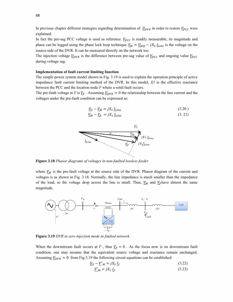
68
In previous chapter different strategies regarding determination of in order to restore were
explained. In fact the pre-sag PCC voltage is used as reference. is readily measurable, its magnitude and
phase can be logged using the phase lock loop technique. is the voltage on the
source-side of the DVR. It can be measured directly on the network too. The injection voltage is the difference between pre-sag value of and ongoing value
during voltage sag.
Implementation of fault current limiting function The simple power system model shown in Fig. 3.19 is used to explain the operation principle of active impedance fault current limiting method of the DVR. In this model, X1 is the effective reactance between the PCC and the location node F where a solid fault occurs. The pre-fault voltage at F is . Assuming 0 the relationship between the line current and the
voltages under the pre-fault condition can be expressed as:
(3.20 )
(3. 21)
Figure 3.18 Phasor diagrams of voltages in non-faulted lossless feeder where is the pre-fault voltage at the source side of the DVR. Phasor diagram of the current and
voltages is as shown in Fig. 3.18. Normally, the line impedance is much smaller than the impedance of the load, so the voltage drop across the line is small. Thus, and have almost the same
magnitude.
Figure 3.19 DVR in zero injection mode in faulted network
When the downstream fault occurs at F , thus 0 . As the focus now is on downstream fault
condition, one may assume that the equivalent source voltage and reactance remain unchanged. Assuming 0 from Fig.3.19 the following circuit equations can be established:
′ (3.22)
′ (3.23)
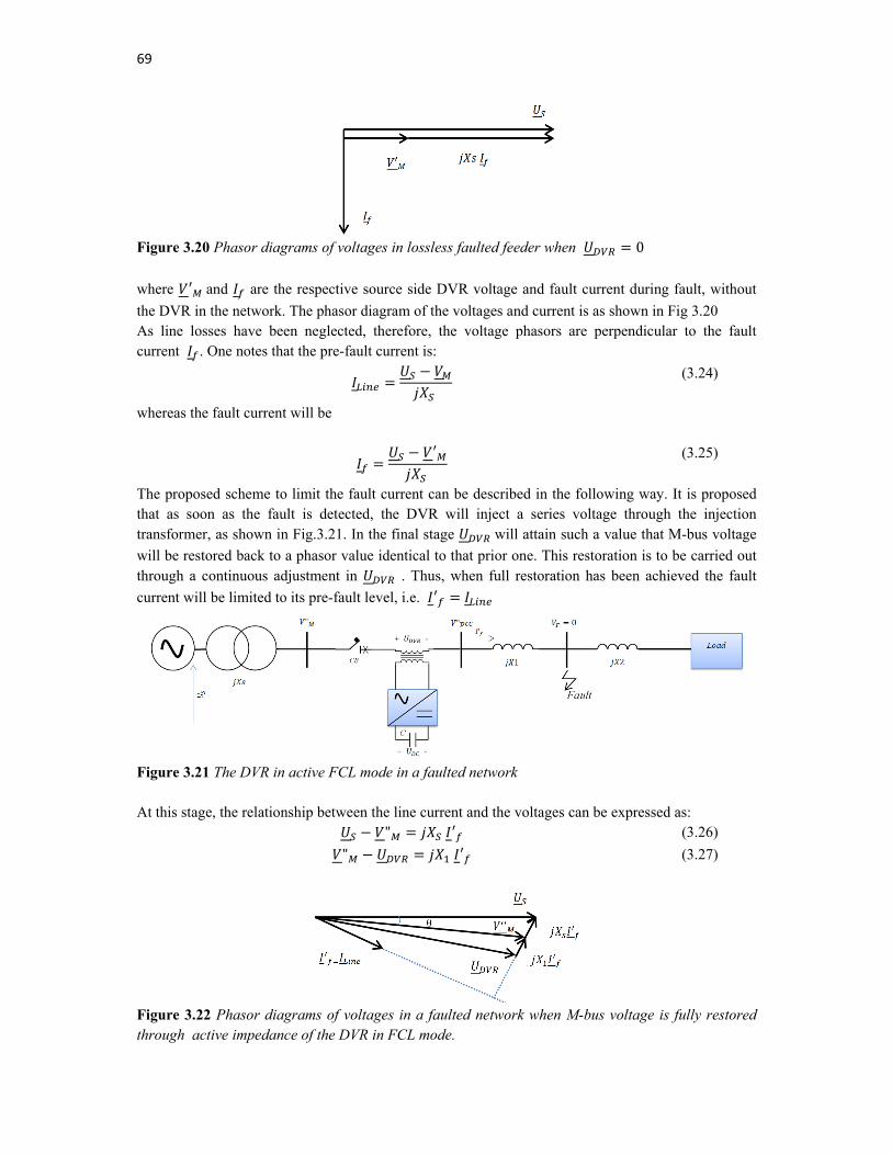
69
Figure 3.20 Phasor diagrams of voltages in lossless faulted feeder when 0
where ′ and are the respective source side DVR voltage and fault current during fault, without
the DVR in the network. The phasor diagram of the voltages and current is as shown in Fig 3.20 As line losses have been neglected, therefore, the voltage phasors are perpendicular to the fault current . One notes that the pre-fault current is:
(3.24)
whereas the fault current will be
′
(3.25)
The proposed scheme to limit the fault current can be described in the following way. It is proposed that as soon as the fault is detected, the DVR will inject a series voltage through the injection transformer, as shown in Fig.3.21. In the final stage will attain such a value that M-bus voltage
will be restored back to a phasor value identical to that prior one. This restoration is to be carried out through a continuous adjustment in . Thus, when full restoration has been achieved the fault
current will be limited to its pre-fault level, i.e. ′
Figure 3.21 The DVR in active FCL mode in a faulted network At this stage, the relationship between the line current and the voltages can be expressed as:
" ′ (3.26)
" ′ (3.27)
Figure 3.22 Phasor diagrams of voltages in a faulted network when M-bus voltage is fully restored through active impedance of the DVR in FCL mode.
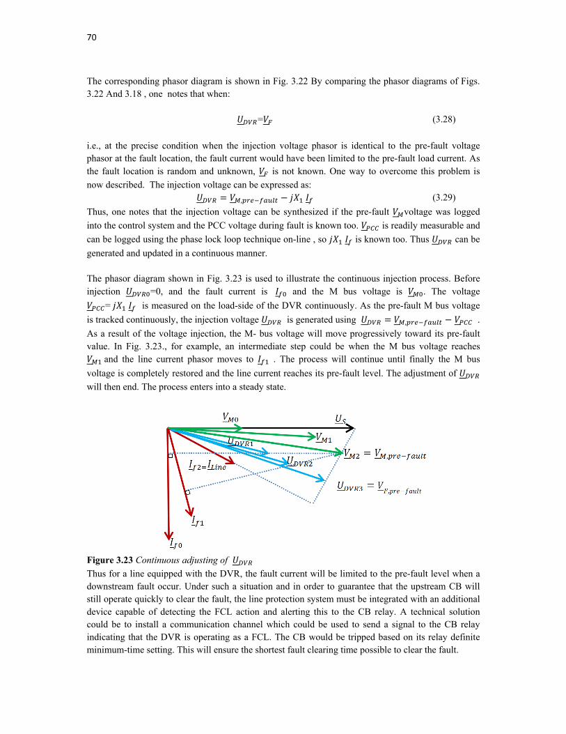
70
The corresponding phasor diagram is shown in Fig. 3.22 By comparing the phasor diagrams of Figs. 3.22 And 3.18 , one notes that when:
= (3.28)
i.e., at the precise condition when the injection voltage phasor is identical to the pre-fault voltage phasor at the fault location, the fault current would have been limited to the pre-fault load current. As the fault location is random and unknown, is not known. One way to overcome this problem is
now described. The injection voltage can be expressed as:
, (3.29)
Thus, one notes that the injection voltage can be synthesized if the pre-fault voltage was logged
into the control system and the PCC voltage during fault is known too. is readily measurable and
can be logged using the phase lock loop technique on-line , so is known too. Thus can be
generated and updated in a continuous manner. The phasor diagram shown in Fig. 3.23 is used to illustrate the continuous injection process. Before injection =0, and the fault current is and the M bus voltage is . The voltage
= is measured on the load-side of the DVR continuously. As the pre-fault M bus voltage
is tracked continuously, the injection voltage is generated using , .
As a result of the voltage injection, the M- bus voltage will move progressively toward its pre-fault value. In Fig. 3.23., for example, an intermediate step could be when the M bus voltage reaches
and the line current phasor moves to . The process will continue until finally the M bus
voltage is completely restored and the line current reaches its pre-fault level. The adjustment of
will then end. The process enters into a steady state.
Figure 3.23 Continuous adjusting of
Thus for a line equipped with the DVR, the fault current will be limited to the pre-fault level when a downstream fault occur. Under such a situation and in order to guarantee that the upstream CB will still operate quickly to clear the fault, the line protection system must be integrated with an additional device capable of detecting the FCL action and alerting this to the CB relay. A technical solution could be to install a communication channel which could be used to send a signal to the CB relay indicating that the DVR is operating as a FCL. The CB would be tripped based on its relay definite minimum-time setting. This will ensure the shortest fault clearing time possible to clear the fault.
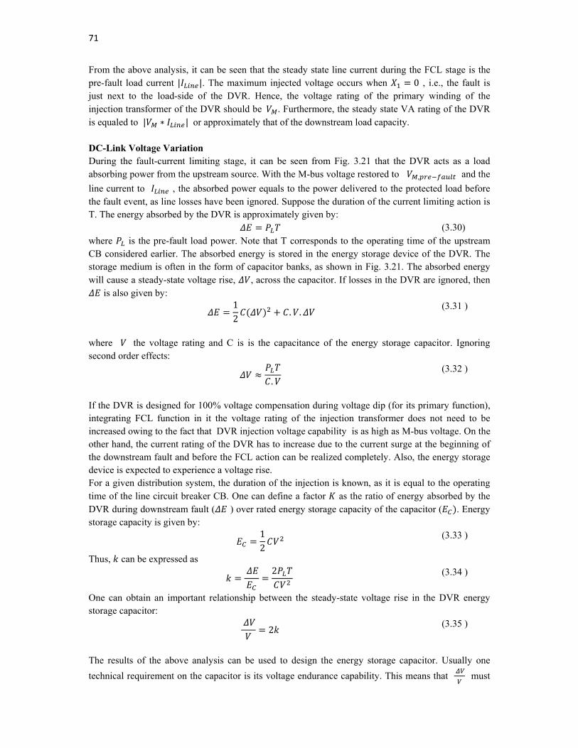
71
From the above analysis, it can be seen that the steady state line current during the FCL stage is the pre-fault load current | |. The maximum injected voltage occurs when 0 , i.e., the fault is just next to the load-side of the DVR. Hence, the voltage rating of the primary winding of the injection transformer of the DVR should be . Furthermore, the steady state VA rating of the DVR is equaled to | ∗ | or approximately that of the downstream load capacity. DC-Link Voltage Variation During the fault-current limiting stage, it can be seen from Fig. 3.21 that the DVR acts as a load absorbing power from the upstream source. With the M-bus voltage restored to , and the
line current to , the absorbed power equals to the power delivered to the protected load before the fault event, as line losses have been ignored. Suppose the duration of the current limiting action is T. The energy absorbed by the DVR is approximately given by:
(3.30) where is the pre-fault load power. Note that T corresponds to the operating time of the upstream CB considered earlier. The absorbed energy is stored in the energy storage device of the DVR. The storage medium is often in the form of capacitor banks, as shown in Fig. 3.21. The absorbed energy will cause a steady-state voltage rise, , across the capacitor. If losses in the DVR are ignored, then
is also given by:
12
. . (3.31 )
where the voltage rating and C is is the capacitance of the energy storage capacitor. Ignoring second order effects:
.
(3.32 )
If the DVR is designed for 100% voltage compensation during voltage dip (for its primary function), integrating FCL function in it the voltage rating of the injection transformer does not need to be increased owing to the fact that DVR injection voltage capability is as high as M-bus voltage. On the other hand, the current rating of the DVR has to increase due to the current surge at the beginning of the downstream fault and before the FCL action can be realized completely. Also, the energy storage device is expected to experience a voltage rise. For a given distribution system, the duration of the injection is known, as it is equal to the operating time of the line circuit breaker CB. One can define a factor as the ratio of energy absorbed by the DVR during downstream fault ( ) over rated energy storage capacity of the capacitor ( . Energy storage capacity is given by:
12
(3.33 )
Thus, can be expressed as 2
(3.34 )
One can obtain an important relationship between the steady-state voltage rise in the DVR energy storage capacitor:
2 (3.35 )
The results of the above analysis can be used to design the energy storage capacitor. Usually one
technical requirement on the capacitor is its voltage endurance capability. This means that
must
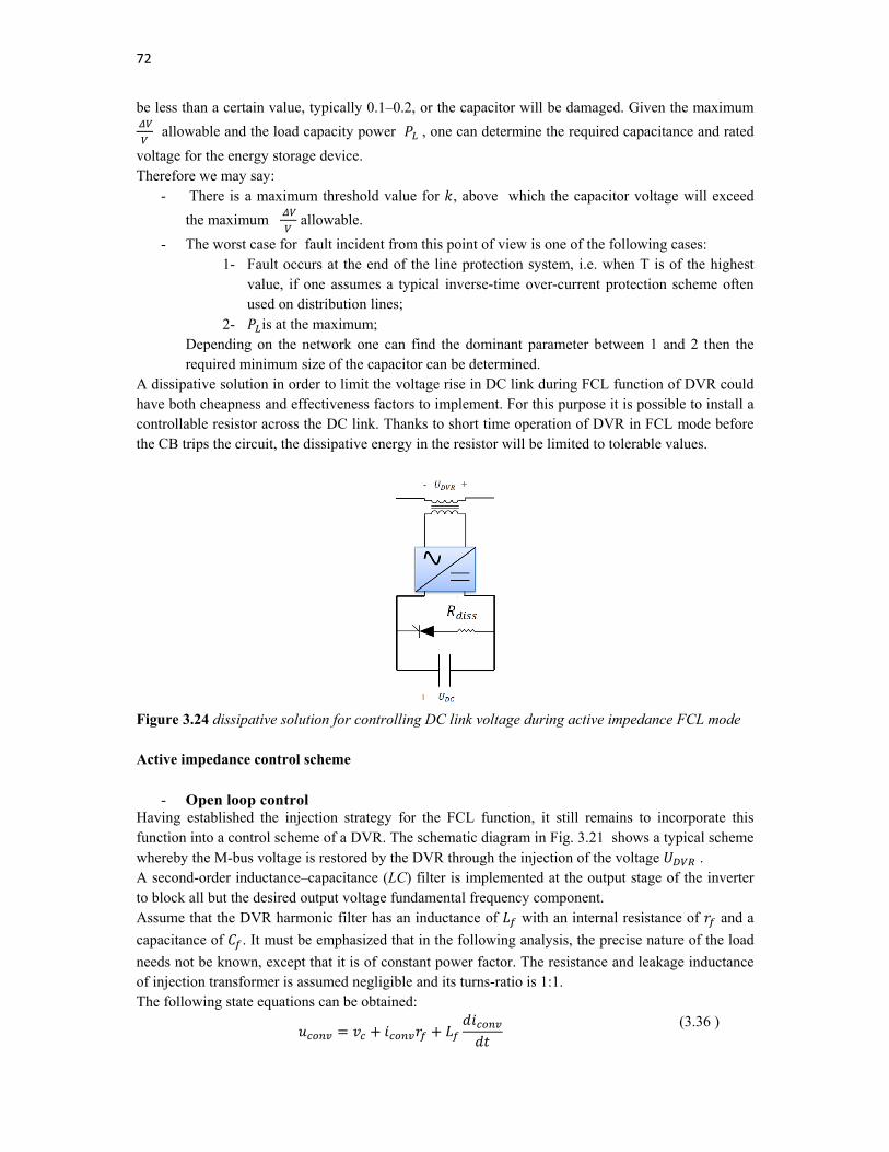
72
be less than a certain value, typically 0.1–0.2, or the capacitor will be damaged. Given the maximum
allowable and the load capacity power , one can determine the required capacitance and rated
voltage for the energy storage device. Therefore we may say:
- There is a maximum threshold value for , above which the capacitor voltage will exceed
the maximum
allowable.
- The worst case for fault incident from this point of view is one of the following cases: 1- Fault occurs at the end of the line protection system, i.e. when T is of the highest
value, if one assumes a typical inverse-time over-current protection scheme often used on distribution lines;
2- is at the maximum; Depending on the network one can find the dominant parameter between 1 and 2 then the required minimum size of the capacitor can be determined.
A dissipative solution in order to limit the voltage rise in DC link during FCL function of DVR could have both cheapness and effectiveness factors to implement. For this purpose it is possible to install a controllable resistor across the DC link. Thanks to short time operation of DVR in FCL mode before the CB trips the circuit, the dissipative energy in the resistor will be limited to tolerable values.
Figure 3.24 dissipative solution for controlling DC link voltage during active impedance FCL mode Active impedance control scheme
- Open loop control Having established the injection strategy for the FCL function, it still remains to incorporate this function into a control scheme of a DVR. The schematic diagram in Fig. 3.21 shows a typical scheme whereby the M-bus voltage is restored by the DVR through the injection of the voltage . A second-order inductance–capacitance (LC) filter is implemented at the output stage of the inverter to block all but the desired output voltage fundamental frequency component. Assume that the DVR harmonic filter has an inductance of with an internal resistance of and a
capacitance of . It must be emphasized that in the following analysis, the precise nature of the load
needs not be known, except that it is of constant power factor. The resistance and leakage inductance of injection transformer is assumed negligible and its turns-ratio is 1:1. The following state equations can be obtained:
(3.36 )
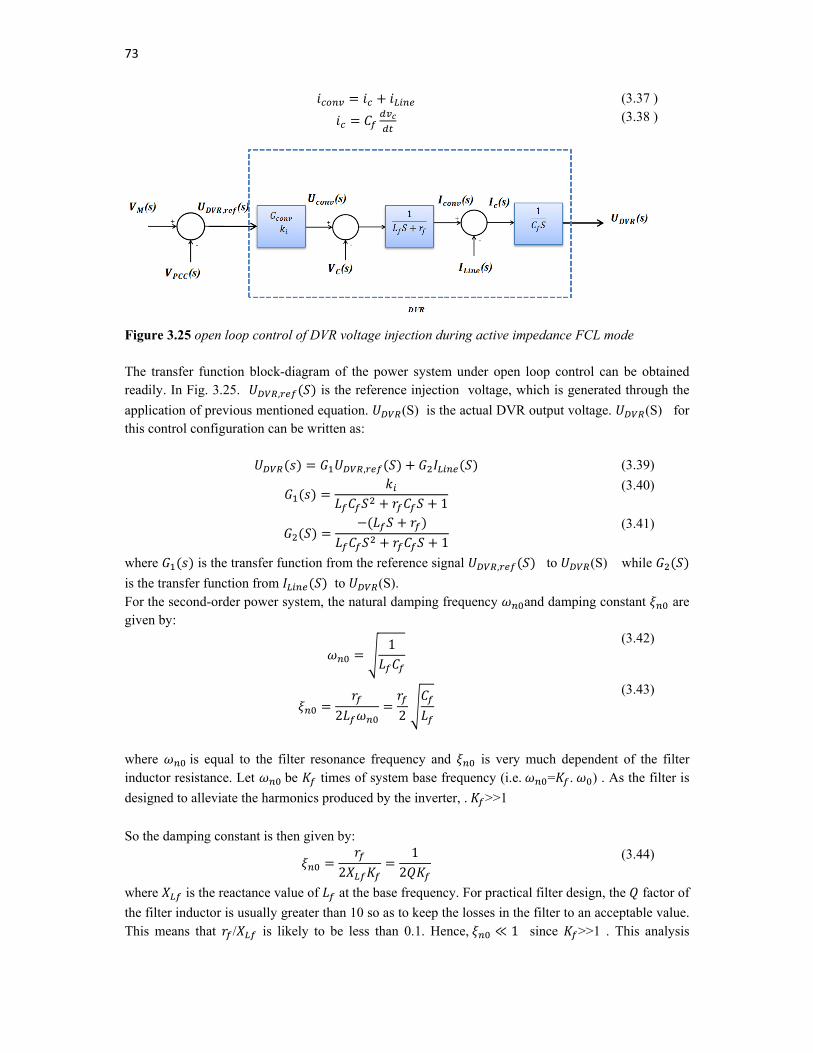
73
(3.37 )
(3.38 )
Figure 3.25 open loop control of DVR voltage injection during active impedance FCL mode The transfer function block-diagram of the power system under open loop control can be obtained readily. In Fig. 3.25. , is the reference injection voltage, which is generated through the
application of previous mentioned equation. (S) is the actual DVR output voltage. (S) for this control configuration can be written as:
, (3.39)
1
(3.40)
1
(3.41)
where is the transfer function from the reference signal , to (S) while
is the transfer function from to (S). For the second-order power system, the natural damping frequency and damping constant are given by:
1
(3.42)
2 2
(3.43)
where is equal to the filter resonance frequency and is very much dependent of the filter inductor resistance. Let be times of system base frequency (i.e. = . ) . As the filter is
designed to alleviate the harmonics produced by the inverter, . >>1
So the damping constant is then given by:
21
2
(3.44)
where is the reactance value of at the base frequency. For practical filter design, the factor of
the filter inductor is usually greater than 10 so as to keep the losses in the filter to an acceptable value. This means that / is likely to be less than 0.1. Hence, ≪ 1 since >>1 . This analysis
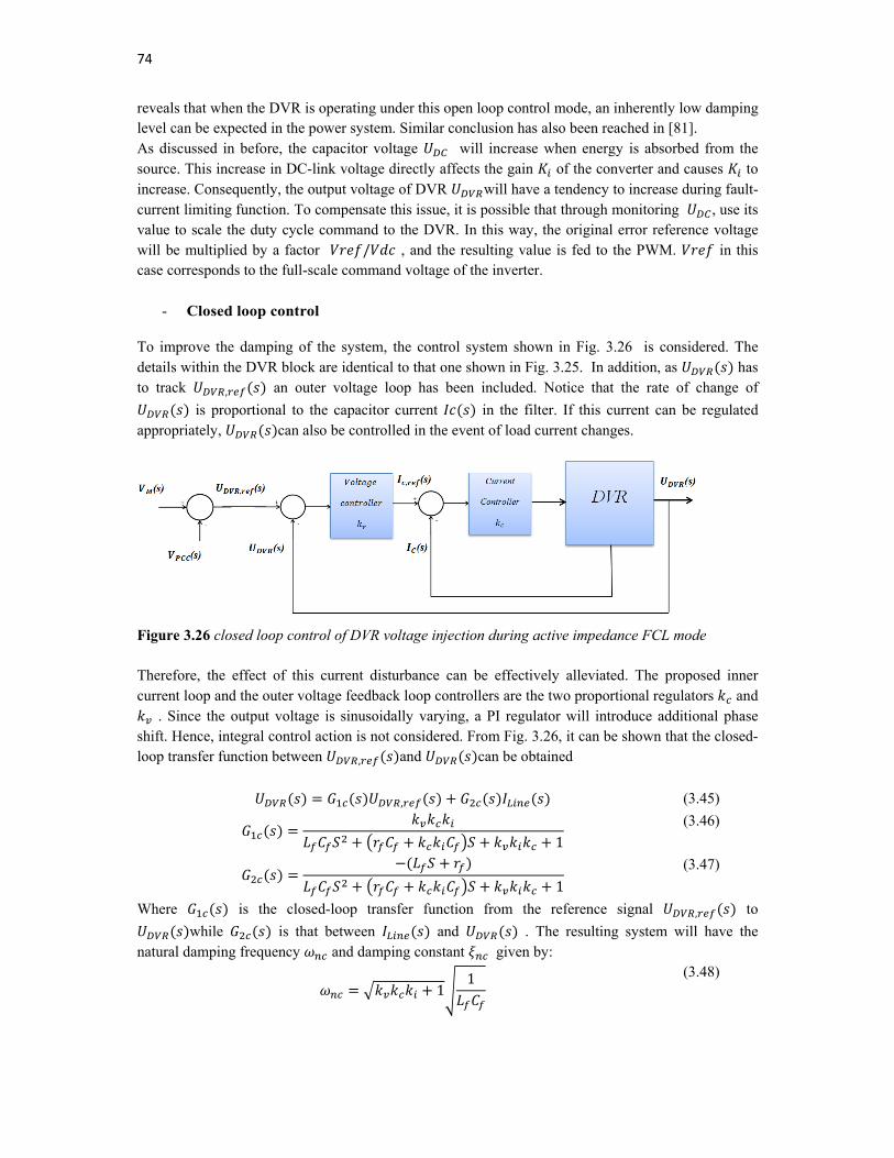
74
reveals that when the DVR is operating under this open loop control mode, an inherently low damping level can be expected in the power system. Similar conclusion has also been reached in [81]. As discussed in before, the capacitor voltage will increase when energy is absorbed from the source. This increase in DC-link voltage directly affects the gain of the converter and causes to increase. Consequently, the output voltage of DVR will have a tendency to increase during fault-current limiting function. To compensate this issue, it is possible that through monitoring , use its value to scale the duty cycle command to the DVR. In this way, the original error reference voltage will be multiplied by a factor / , and the resulting value is fed to the PWM. in this case corresponds to the full-scale command voltage of the inverter.
- Closed loop control
To improve the damping of the system, the control system shown in Fig. 3.26 is considered. The details within the DVR block are identical to that one shown in Fig. 3.25. In addition, as has to track , an outer voltage loop has been included. Notice that the rate of change of
is proportional to the capacitor current in the filter. If this current can be regulated appropriately, can also be controlled in the event of load current changes.
Figure 3.26 closed loop control of DVR voltage injection during active impedance FCL mode Therefore, the effect of this current disturbance can be effectively alleviated. The proposed inner current loop and the outer voltage feedback loop controllers are the two proportional regulators and
. Since the output voltage is sinusoidally varying, a PI regulator will introduce additional phase shift. Hence, integral control action is not considered. From Fig. 3.26, it can be shown that the closed-loop transfer function between , and can be obtained
, (3.45)
1
(3.46)
1
(3.47)
Where is the closed-loop transfer function from the reference signal , to
while is that between and . The resulting system will have the natural damping frequency and damping constant given by:
11
(3.48)
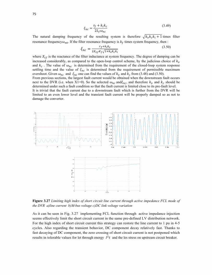
75
2
(3.49)
The natural damping frequency of the resulting system is therefore 1times filter
resonance frequency . If the filter resonance frequency is times system frequency, then :
(3.50)
where is the reactance of the filter inductance at system frequency. The degree of damping can be increased considerably, as compared to the open-loop control scheme, by the judicious choice of and . The value of is determined from the requirement of the closed-loop system response settling time and the value of is determined from the requirement of permissible maximum overshoot. Given and one can find the values of and from (3.48) and (3.50). From previous sections, the largest fault current would be obtained when the downstream fault occurs next to the DVR (i.e. when X1=0). So the selected and , and therefore and should be determined under such a fault condition so that the fault current is limited close to its pre-fault level. It is trivial that the fault current due to a downstream fault which is further from the DVR will be limited to an even lower level and the transient fault current will be properly damped so as not to damage the converter.
Figure 3.27 Limiting high index of short circuit line current through active impedance FCL mode of the DVR a)line current b)M-bus voltage c)DC link voltage variation
As it can be seen in Fig. 3.27 implementing FCL function through active impedance injection seems effectively limit the short circuit current in the same pre-defined LV distribution network. For the high index of short circuit current this strategy can restore the line current to 1 pu in 4-5 cycles. Also regarding the transient behavior, DC component decay relatively fast. Thanks to fast decaying of DC component, the zero crossing of short circuit current is not postponed which results in tolerable values for let through energy and the les stress on upstream circuit breaker.
Cur
rent
[pu]
0.4 0.45 0.5 0.55 0.6 0.65 0.7
Time(S)
0
100
200
300
400
500
600
700

76
3.6.2 Active reactance FCL strategy Voltage injection in-phase with the line voltage gives the minimal voltage injection requirement for the DVR during FCL operation mode; however, as already discussed, controlling the DVR as a virtual inductor would ensure zero real power absorption during downstream fault current limiting function thus guarantees a constant DC link voltage. Furthermore in feeders with dominant inductive impedance (like MV level feeders) the active reactance strategy for DVR FCL function is carried out through an injected voltage which is almost in phase with , therefore it gives approximately minimal voltage injection requirement. Also for a nearby fault, where ≫ (equivalent to; ≫ , magnitudes of , and , would be similar in Fig 3.16.
Realizing the active reactance through the DVR is achieved through different strategies. Each strategy has its own pros and cons and it is impossible to say surely which one is the best choice. Therefore a dedicated case study based on a real network and its requirements in order to employ the best choice is required.
These strategies includes:
1- Constant active reactance - Flux-charge control strategy; - Voltage-current control strategy;
2- Variable active reactance
Constant active reactance
- Flux –charge control scheme Fig. 3.15 shows a downstream fault occurring in the DVR connected system. Using the voltage divider concept, the fault current and M-bus voltage in this fault situation can be calculated as (with the DVR bypassed and without consideration of other feeders connected at M-bus)
(3.51)
(3.52)
Where is the source impedance and is the downstream feeder impedance including the fault
impedance. Due to the very low line impedance, the fault current would be significant as it can be seen from (3.51). As illustrated in (3.52), the M-bus voltage will drop and the remaining voltage can be very low with a
small (a nearby fault). The sag in will affect the loads on the other parallel feeders
connected to M-bus too. The DVR, acting as an inductance, would therefore compensate the fault current by generating nearly 1 per-unit voltage lagging the fault current by 90 with no real power absorption. By representing the DVR as an inductance in series, the fault current and M-bus voltage can be recalculated as:
(3.53)
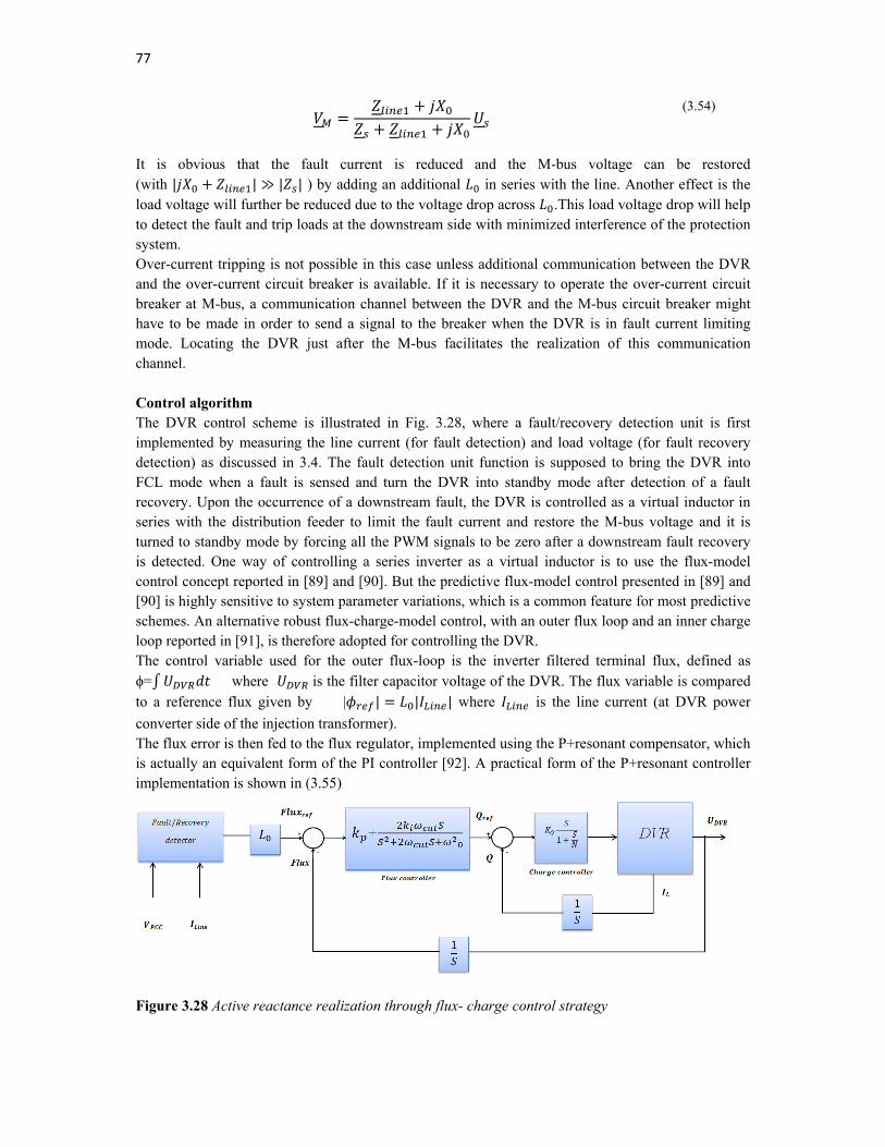
77
(3.54)
It is obvious that the fault current is reduced and the M-bus voltage can be restored (with | | ≫ | | ) by adding an additional in series with the line. Another effect is the load voltage will further be reduced due to the voltage drop across .This load voltage drop will help to detect the fault and trip loads at the downstream side with minimized interference of the protection system. Over-current tripping is not possible in this case unless additional communication between the DVR and the over-current circuit breaker is available. If it is necessary to operate the over-current circuit breaker at M-bus, a communication channel between the DVR and the M-bus circuit breaker might have to be made in order to send a signal to the breaker when the DVR is in fault current limiting mode. Locating the DVR just after the M-bus facilitates the realization of this communication channel. Control algorithm The DVR control scheme is illustrated in Fig. 3.28, where a fault/recovery detection unit is first implemented by measuring the line current (for fault detection) and load voltage (for fault recovery detection) as discussed in 3.4. The fault detection unit function is supposed to bring the DVR into FCL mode when a fault is sensed and turn the DVR into standby mode after detection of a fault recovery. Upon the occurrence of a downstream fault, the DVR is controlled as a virtual inductor in series with the distribution feeder to limit the fault current and restore the M-bus voltage and it is turned to standby mode by forcing all the PWM signals to be zero after a downstream fault recovery is detected. One way of controlling a series inverter as a virtual inductor is to use the flux-model control concept reported in [89] and [90]. But the predictive flux-model control presented in [89] and [90] is highly sensitive to system parameter variations, which is a common feature for most predictive schemes. An alternative robust flux-charge-model control, with an outer flux loop and an inner charge loop reported in [91], is therefore adopted for controlling the DVR. The control variable used for the outer flux-loop is the inverter filtered terminal flux, defined as ϕ= where is the filter capacitor voltage of the DVR. The flux variable is compared to a reference flux given by | | | | where is the line current (at DVR power
converter side of the injection transformer). The flux error is then fed to the flux regulator, implemented using the P+resonant compensator, which is actually an equivalent form of the PI controller [92]. A practical form of the P+resonant controller implementation is shown in (3.55)
Figure 3.28 Active reactance realization through flux- charge control strategy
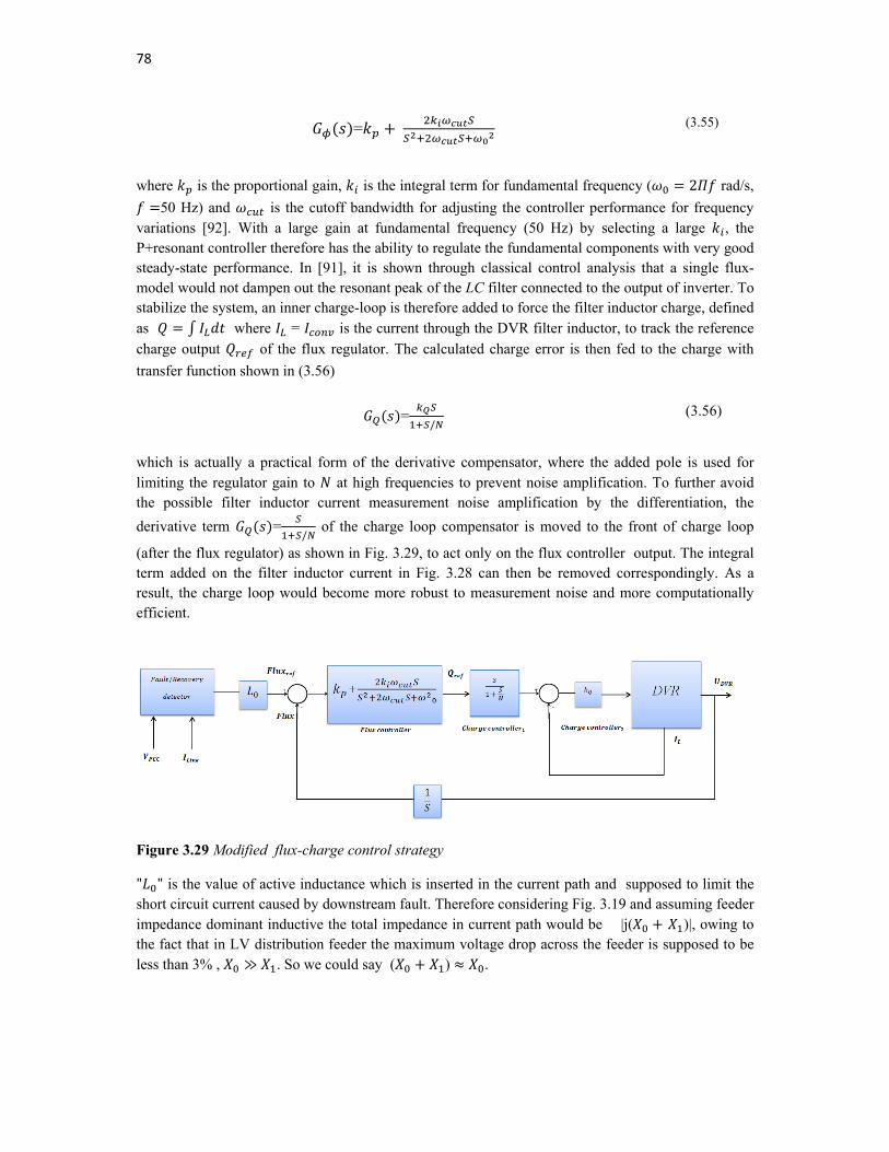
78
= (3.55)
where is the proportional gain, is the integral term for fundamental frequency ( 2 rad/s,
50 Hz) and is the cutoff bandwidth for adjusting the controller performance for frequency variations [92]. With a large gain at fundamental frequency (50 Hz) by selecting a large , the P+resonant controller therefore has the ability to regulate the fundamental components with very good steady-state performance. In [91], it is shown through classical control analysis that a single flux-model would not dampen out the resonant peak of the LC filter connected to the output of inverter. To stabilize the system, an inner charge-loop is therefore added to force the filter inductor charge, defined as where = is the current through the DVR filter inductor, to track the reference charge output of the flux regulator. The calculated charge error is then fed to the charge with
transfer function shown in (3.56)
=/
(3.56)
which is actually a practical form of the derivative compensator, where the added pole is used for limiting the regulator gain to at high frequencies to prevent noise amplification. To further avoid the possible filter inductor current measurement noise amplification by the differentiation, the
derivative term =/
of the charge loop compensator is moved to the front of charge loop
(after the flux regulator) as shown in Fig. 3.29, to act only on the flux controller output. The integral term added on the filter inductor current in Fig. 3.28 can then be removed correspondingly. As a result, the charge loop would become more robust to measurement noise and more computationally efficient.
Figure 3.29 Modified flux-charge control strategy
" " is the value of active inductance which is inserted in the current path and supposed to limit the short circuit current caused by downstream fault. Therefore considering Fig. 3.19 and assuming feeder impedance dominant inductive the total impedance in current path would be |j( )|, owing to the fact that in LV distribution feeder the maximum voltage drop across the feeder is supposed to be less than 3% , ≫ . So we could say ( ) .
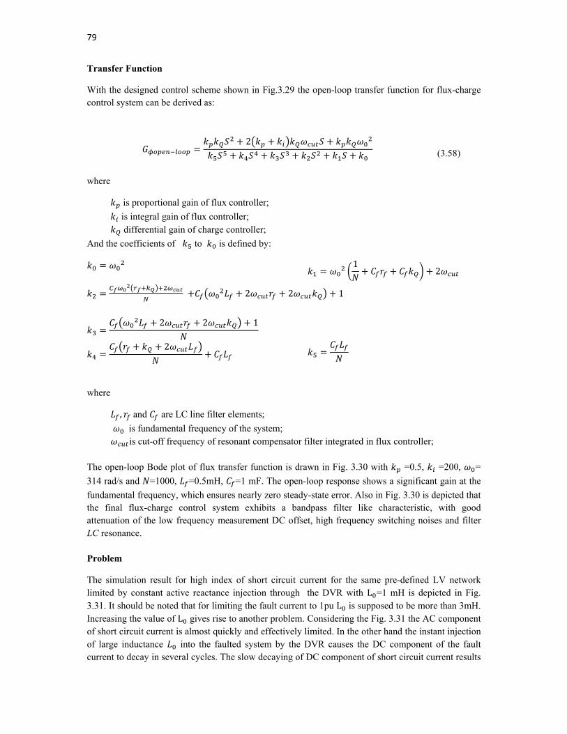
79
Transfer Function
With the designed control scheme shown in Fig.3.29 the open-loop transfer function for flux-charge control system can be derived as:
2
(3.58)
where
is proportional gain of flux controller;
is integral gain of flux controller; differential gain of charge controller;
And the coefficients of to is defined by:
12
2 2 1
2 2 1
2
where
, and are LC line filter elements;
is fundamental frequency of the system; is cut-off frequency of resonant compensator filter integrated in flux controller;
The open-loop Bode plot of flux transfer function is drawn in Fig. 3.30 with =0.5, =200, =
314 rad/s and =1000, =0.5mH, =1 mF. The open-loop response shows a significant gain at the
fundamental frequency, which ensures nearly zero steady-state error. Also in Fig. 3.30 is depicted that the final flux-charge control system exhibits a bandpass filter like characteristic, with good attenuation of the low frequency measurement DC offset, high frequency switching noises and filter LC resonance. Problem
The simulation result for high index of short circuit current for the same pre-defined LV network limited by constant active reactance injection through the DVR with L =1 mH is depicted in Fig. 3.31. It should be noted that for limiting the fault current to 1pu L is supposed to be more than 3mH. Increasing the value of L gives rise to another problem. Considering the Fig. 3.31 the AC component of short circuit current is almost quickly and effectively limited. In the other hand the instant injection of large inductance into the faulted system by the DVR causes the DC component of the fault current to decay in several cycles. The slow decaying of DC component of short circuit current results
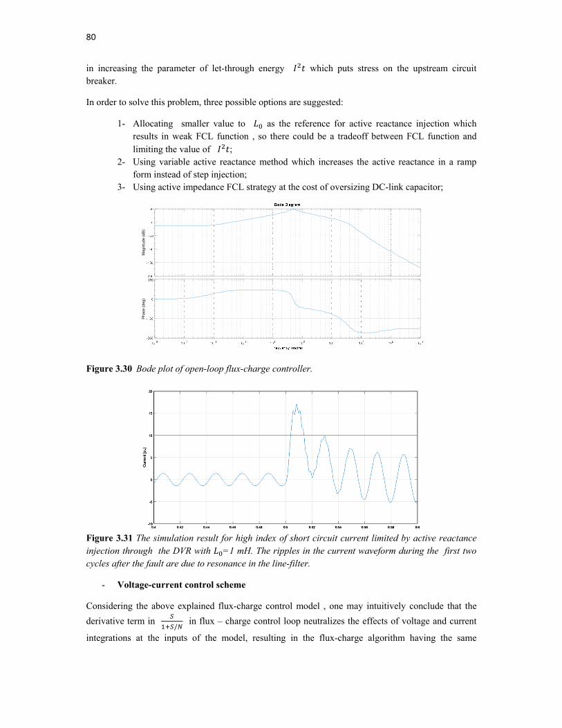
80
in increasing the parameter of let-through energy which puts stress on the upstream circuit breaker.
In order to solve this problem, three possible options are suggested:
1- Allocating smaller value to as the reference for active reactance injection which results in weak FCL function , so there could be a tradeoff between FCL function and limiting the value of ;
2- Using variable active reactance method which increases the active reactance in a ramp form instead of step injection;
3- Using active impedance FCL strategy at the cost of oversizing DC-link capacitor;
Figure 3.30 Bode plot of open-loop flux-charge controller.
Figure 3.31 The simulation result for high index of short circuit current limited by active reactance injection through the DVR with =1 mH. The ripples in the current waveform during the first two cycles after the fault are due to resonance in the line-filter.
- Voltage-current control scheme
Considering the above explained flux-charge control model , one may intuitively conclude that the
derivative term in /
in flux – charge control loop neutralizes the effects of voltage and current
integrations at the inputs of the model, resulting in the flux-charge algorithm having the same
Mag
nitu
de (
dB)
Pha
se (
deg)
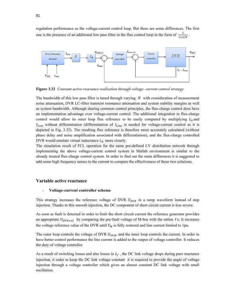
81
regulation performance as the voltage-current control loop. But there are some differences. The first
one is the presence of an additional low pass filter in the flux control loop in the form of /
.
Figure 3.32 Constant active reactance realization through voltage- current control strategy
The bandwidth of this low pass filter is tuned through varying with consideration of measurement noise attenuation, DVR LC-filter transient resonance attenuation and system stability margins as well as system bandwidth. Although sharing common control principles, the flux-charge control does have an implementation advantage over voltage-current control. The additional integration in flux-charge control would allow its outer loop flux reference to be easily computed by multiplying and
without differentiation (differentiation of is needed for voltage-current control as it is depicted in Fig. 3.32). The resulting flux reference is therefore more accurately calculated (without phase delay and noise amplification associated with differentiation), and the flux-charge controlled DVR would emulate virtual inductance more closely. The simulation result of FCL operation for the same pre-defined LV distribution network through implementing the above voltage-current control system in Matlab environment is similar to the already treated flux-charge control system. In order to find out the main differences it is suggested to add some high frequency noises to the current to compare the effectiveness of these two solutions.
Variable active reactance
- Voltage-current controller scheme
This strategy increases the reference voltage of DVR in a ramp waveform instead of step injection. Thanks to this smooth injection, the DC component of short circuit current is less severe.
As soon as fault is detected in order to limit the short circuit current the reference generator provides an appropriate , by comparing the pre-fault voltage of M-bus with the online VM. It increases
the voltage reference value of the DVR until is fully restored and line current limited to 1pu.
The outer loop controls the voltage of DVR , and the inner loop controls the current. In order to have better control performance the line current is added to the output of voltage controller. It reduces the duty of voltage controller.
As a result of switching losses and also losses in , the DC link voltage drops during pure reactance
injection, it order to keep the DC link voltage constant it is required to provide the angle of voltage injection through a voltage controller which gives an almost constant DC link voltage with small oscillation.
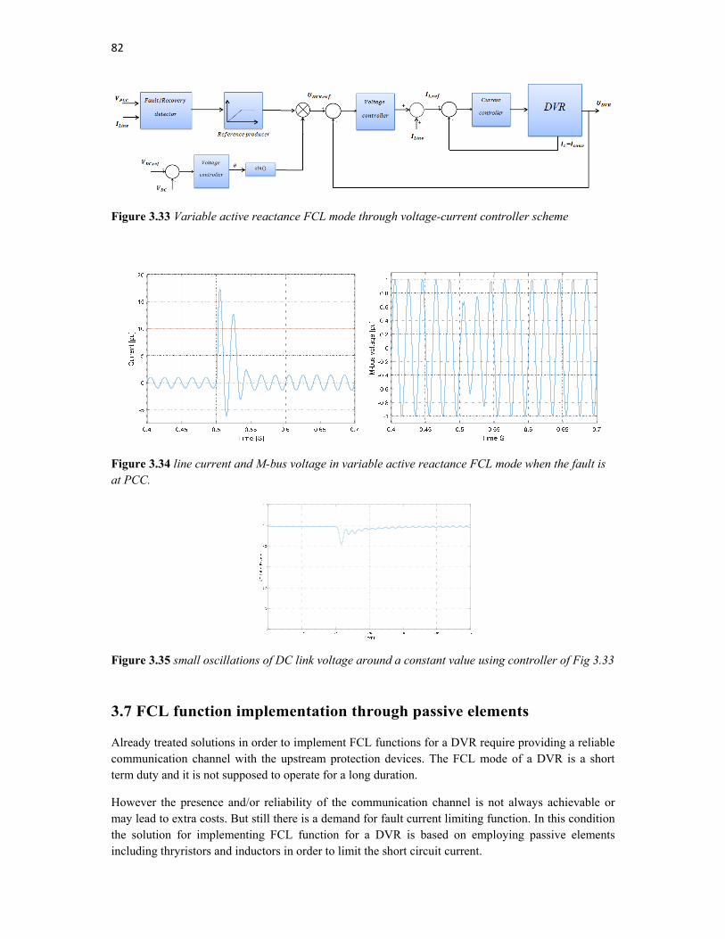
82
Figure 3.33 Variable active reactance FCL mode through voltage-current controller scheme
Figure 3.34 line current and M-bus voltage in variable active reactance FCL mode when the fault is at PCC.
Figure 3.35 small oscillations of DC link voltage around a constant value using controller of Fig 3.33
3.7 FCL function implementation through passive elements
Already treated solutions in order to implement FCL functions for a DVR require providing a reliable communication channel with the upstream protection devices. The FCL mode of a DVR is a short term duty and it is not supposed to operate for a long duration.
However the presence and/or reliability of the communication channel is not always achievable or may lead to extra costs. But still there is a demand for fault current limiting function. In this condition the solution for implementing FCL function for a DVR is based on employing passive elements including thryristors and inductors in order to limit the short circuit current.

83
Due to the fact that there is no communication between DVR and upstream circuit breaker during the next sections we are trying to limit our high index of short circuit current (when fault occurs at PCC) as close as possible to 10 and at the same time we are taking to account the limitation imposed on our low index of short circuit current (when fault occurs at load-bus) in such a way that still can be detected by upstream circuit breaker and have the chance to be cleared instantaneously in order not to interfere with pre-set protection coordination. If both aims are achieved then we can have an appropriate solution for FCL function through passive elements.
3.7.1 Using the impedance of the injection transformer
Figure 3.36 FCL operation through impedance of injection transformer
This protection strategy is the most conventional one for series devices which is also analyze in [29]. In [29] an integrated protection scheme with varistors, thyristors and mechanical bypass are proposed. The idea is ensuring an alternative current to avoid interference with the existing protection equipment and the uncontrolled charging of the DC-link. In several DVR protection schemes thyristors are intended to take over the current for the VSC until a more robust and slower mechanically bypass is ensured. This method is explained in this way, as soon as fault is detected:
1- Zero-state condition is applied to the inverter. The IGBTs are supposed to tolerate the flow of short circuit current (in terms of both electromagnetic forces and also thermal limitation) for some micro seconds prior to realization of FCL function;
2- Control system turns on anti-parallel thyristors. Thyristors react fast and by taking advantage
of short circuit impedance of injection transformer which is saturated during short circuit, limits the fault current considerably;
The configuration of this strategy is depicted if Fig. 3.36. Varistors can be considered as a voltage dependent resistance and cannot ensure a continuous current path, but they can be used to detect and limit voltage spikes across the DVR. Varistors must effectively be placed at the secondary side of the injection transformers. The simulation results of this configuration in Matlab environment for the same pre-defined LV network with the parameter in table 3.1 are depicted in Fig. 3.37 for fault at PCC and in Fig. 3.39 for fault at load-bus.
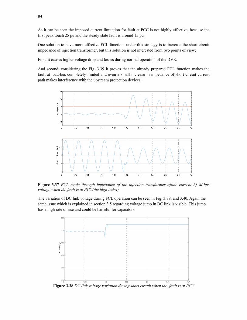
84
As it can be seen the imposed current limitation for fault at PCC is not highly effective, because the first peak touch 25 pu and the steady state fault is around 15 pu.
One solution to have more effective FCL function under this strategy is to increase the short circuit impedance of injection transformer, but this solution is not interested from two points of view;
First, it causes higher voltage drop and losses during normal operation of the DVR.
And second, considering the Fig. 3.39 it proves that the already prepared FCL function makes the fault at load-bus completely limited and even a small increase in impedance of short circuit current path makes interference with the upstream protection devices.
Figure 3.37 FCL mode through impedance of the injection transformer a)line current b) M-bus voltage when the fault is at PCC(the high index)
The variation of DC link voltage during FCL operation can be seen in Fig. 3.38. and 3.40. Again the same issue which is explained in section 3.5 regarding voltage jump in DC link is visible. This jump has a high rate of rise and could be harmful for capacitors.
Figure 3.38 DC link voltage variation during short circuit when the fault is at PCC 0.4 0.45 0.5 0.55 0.6 0.65 0.7
300
350
400
450
500
550
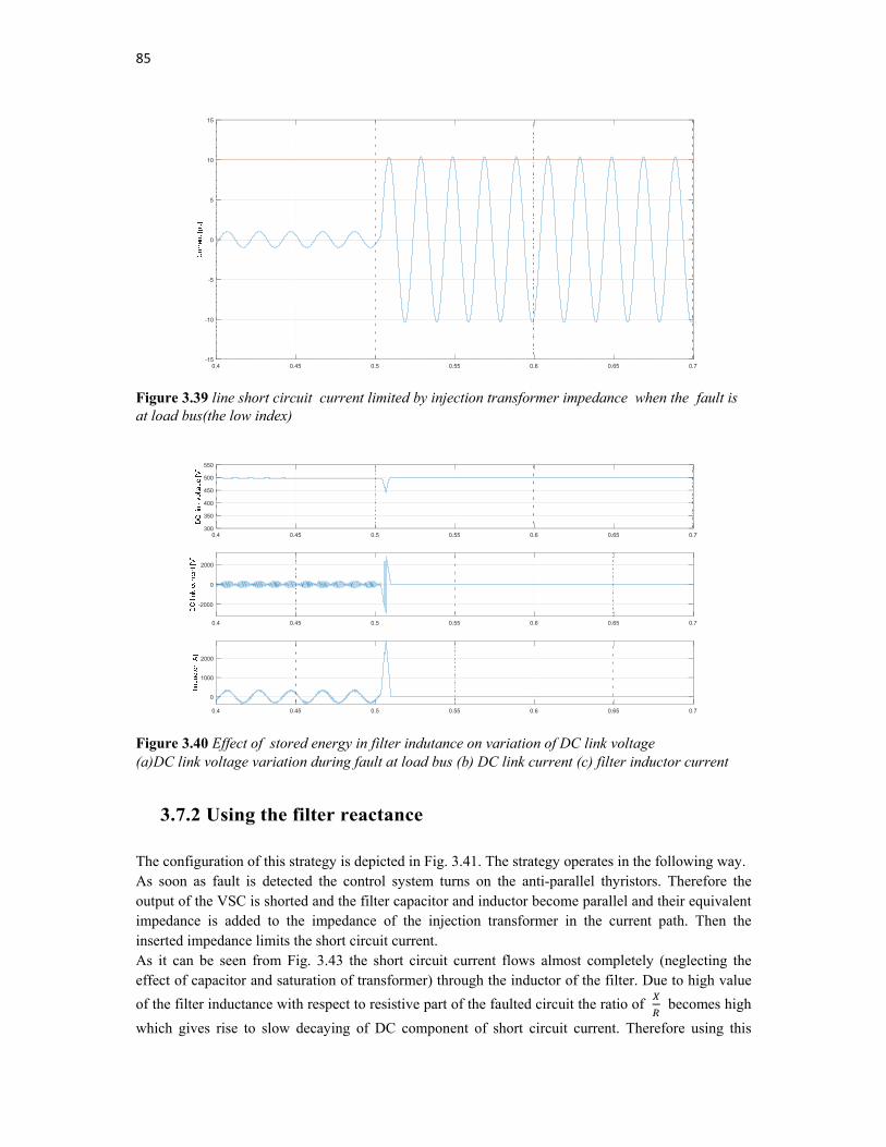
85
Figure 3.39 line short circuit current limited by injection transformer impedance when the fault is at load bus(the low index)
Figure 3.40 Effect of stored energy in filter indutance on variation of DC link voltage (a)DC link voltage variation during fault at load bus (b) DC link current (c) filter inductor current
3.7.2 Using the filter reactance The configuration of this strategy is depicted in Fig. 3.41. The strategy operates in the following way. As soon as fault is detected the control system turns on the anti-parallel thyristors. Therefore the output of the VSC is shorted and the filter capacitor and inductor become parallel and their equivalent impedance is added to the impedance of the injection transformer in the current path. Then the inserted impedance limits the short circuit current. As it can be seen from Fig. 3.43 the short circuit current flows almost completely (neglecting the effect of capacitor and saturation of transformer) through the inductor of the filter. Due to high value
of the filter inductance with respect to resistive part of the faulted circuit the ratio of becomes high
which gives rise to slow decaying of DC component of short circuit current. Therefore using this
0.4 0.45 0.5 0.55 0.6 0.65 0.7-15
-10
-5
0
5
10
15
0.4 0.45 0.5 0.55 0.6 0.65 0.7300
350
400
450
500
550
0.4 0.45 0.5 0.55 0.6 0.65 0.7
-2000
0
2000
0.4 0.45 0.5 0.55 0.6 0.65 0.7
Ti [ ]
0
1000
2000
86
strategy for the same pre-defined LV network postpones the first zero crossing of short circuit current to 6th cycle. This issue results in considerably increasing of the let trough energy which puts a high stress on upstream equipment including the circuit breaker.
Figure 3.41 Implementation of FCL function through filter inductance
A solution for this issue may be decreasing the value of line filter inductor by increasing the switching frequency of the power converter. Unfortunately the switching frequency is limited by several factors including switching losses and limitation of radiated emission imposed by EMC standards.
Decreasing the value of line filter inductor without changing the switching frequency causes increase in THD of line current during normal operation condition which gives rise to other problems in terms of power quality and is not accepted by the IEC standard.
Figure 3.42 Presence of long term DC component in the line current during FCL operation by filter inductance when the fault is at pcc (the high index). The ripples in the current waveform are due to resonance in the line-filter. The short circuit current sharing between the filter capacitor and the filter inductor is depicted in Fig. 3.43. As it can be seen except small oscillation caused by resonance which flows into the filter capacitor all short circuit current flows in the filter inductor which is what we expected because:
≪
0.4 0.45 0.5 0.55 0.6 0.65 0.7-4
-2
0
2
4
6
8
10
12
14
16
87
Regarding the variation in DC link capacitors, as it is shown in Fig 3.44 the reduction of DC link voltage at the fault moment is due to delay of fault detector while thanks to being shorted at the output of the inverter by the thyristors, there is no jump of DC voltage anymore.
Figure 3.43 a)Short circuti line current b)Filter inductor current c)Filter capacitor current
Figure 3.44 Variation of the DC link voltage during FCL operation through filter inductance when the fault is at PCC.Thanks to new path for inductor current there is no jump in the DC link voltage. Presence of fault at the load-bus (low index of short circuit current) is shown in the Fig. 3.45. Due to high value of the filter inductor there is a strong limitation imposed on the short circuit current in such a way that it cannot be detected and cleared by instantaneous operation of the circuit breaker. In conclusion we may say that due to required oversizing in terms of installation location, insolation material and also conductor diameter of filter inductor to be used as a fault current limiting element and also considering the described problems, this strategy for implementing FCL function is not applicable even though it was proposed in some literatures.
0.4 0.42 0.44 0.46 0.48 0.5 0.52 0.54 0.56 0.58 0.6-5
0
5
10
15
0.4 0.42 0.44 0.46 0.48 0.5 0.52 0.54 0.56 0.58 0.6-5
0
5
10
15
0.4 0.42 0.44 0.46 0.48 0.5 0.52 0.54 0.56 0.58 0.6-5
0
5
10
15
DC
link
vol
tage
[V
]
88
Figure 3.45 line short circuit current limited by filter inductance when fault is at load-bus(the low index). The coordination with upstream protection is lost.
3.7.3 Merging the FCL function with the bypass strategy As already explained in part 3.7.1 the best possible outcome of FCL funtion using the impedance of injection transformer as a current limiter gives the value of 25 pu for the highest peak of short circuit current . In this section a new configuration through merging the FCL funtion with bypass solution is proposed. An external reactance of is inserted into the protection scenario which is in series connection with the anti-parallel thyritors. Calculation results together with simulation curves prove that the required value for is a lot less than filter inductor.(around 0.1 .
Figure 3.46 Merging FCL funtion with bypass strategy in order to be more in accordance with upstream protection coordination However thanks to this small indutance a considerable current limiting performance with respect to part 3.7.1 is achieved. At the same time taking advantage of bypass solution gives the possibility in
Cur
rent
[pu]
89
order not to intefere with upstream protection coordination for the fault occuring at the end of the feeder(load-bus) The principle of operation is the following steps:
- As soon as fault is detected the control system puts the VSC in zero- state and the static switch across the capacitor filter is turned on in order to limit the short circuit current;
- The line current is continously sensed and compared with 10 , if it becomes less than 10 the the control system turns on the bypass thyristors to ensure a high short circuit current flows into the feeder in order to be detected and clreaded quickly by the upstream circuit breaker;
For the purpose of finding the value of we can use the following equations to limit the highest posssible short circuit current due to fault at PCC.
′ | ′ ′ , , |
10
(3.59)
where
′ is steady state short circuit current after inserting the reactance of ;
′ and ′ , are respectively saturated short circuit impedance of supply and
injection transformer;
, is the voltage drop across anti-parallel thyristors;
is the reactance of fault current limiting inductor;
Using this equation, and parameter of the pre-defined LV network of table 3.1 gives 60uH
Simulation results of this configuration are depicted in Fig. 3.47 for the fault at PCC and in Fig. 49 for the fault at load-bus.
As it is shown in the Fig. 3.47 the steady state of limited short circuit current is remain above 10 , therefore there is no interference with upstream circuit breaker in terms of protection coordination.
Considering the Fig. 3.49 for the fault at load-bus without using bypass switches, the short circuit current was limited to 8 pu and lost the chance to be detected by instantaneous tripping of circuit breaker. The resulted interference with protection coordination causes harmful effect on the equipment including the DVR injection transformer and also the main grid. Besides for loads in parallel feeder a deep and long term voltage dip is expected.
As a result of merging the bypass solution to FCL function of DVR under this strategy, it gives the possibility to bypass the FCL inductor when the current is less than 10 in order to be detected by the upstream circuit breaker.
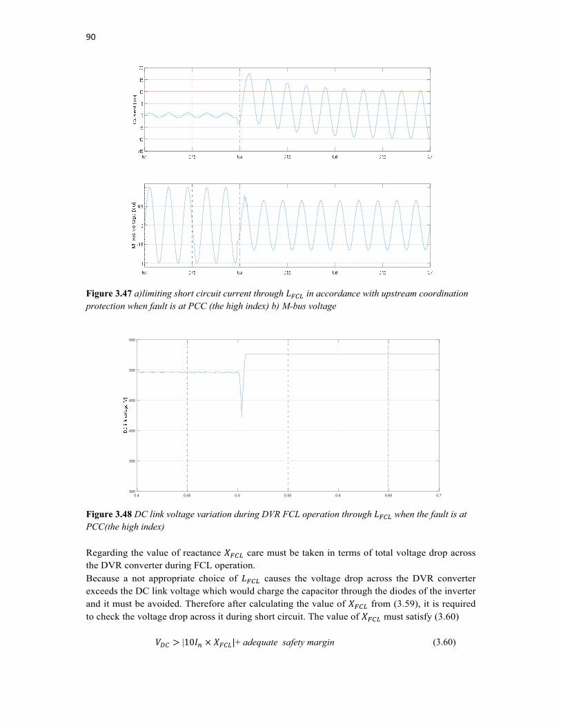
90
Figure 3.47 a)limiting short circuit current through in accordance with upstream coordination protection when fault is at PCC (the high index) b) M-bus voltage
Figure 3.48 DC link voltage variation during DVR FCL operation through when the fault is at PCC(the high index) Regarding the value of reactance care must be taken in terms of total voltage drop across the DVR converter during FCL operation. Because a not appropriate choice of causes the voltage drop across the DVR converter exceeds the DC link voltage which would charge the capacitor through the diodes of the inverter and it must be avoided. Therefore after calculating the value of from (3.59), it is required to check the voltage drop across it during short circuit. The value of must satisfy (3.60)
|10 |+ adequate safety margin (3.60)
0.4 0.45 0.5 0.55 0.6 0.65 0.7300
350
400
450
500
550
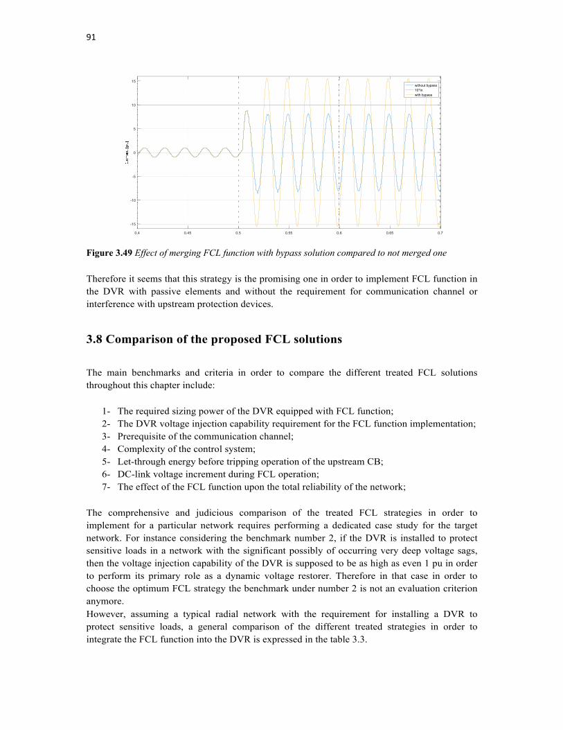
91
Figure 3.49 Effect of merging FCL function with bypass solution compared to not merged one Therefore it seems that this strategy is the promising one in order to implement FCL function in the DVR with passive elements and without the requirement for communication channel or interference with upstream protection devices.
3.8 Comparison of the proposed FCL solutions
The main benchmarks and criteria in order to compare the different treated FCL solutions throughout this chapter include:
1- The required sizing power of the DVR equipped with FCL function; 2- The DVR voltage injection capability requirement for the FCL function implementation; 3- Prerequisite of the communication channel; 4- Complexity of the control system; 5- Let-through energy before tripping operation of the upstream CB; 6- DC-link voltage increment during FCL operation; 7- The effect of the FCL function upon the total reliability of the network;
The comprehensive and judicious comparison of the treated FCL strategies in order to implement for a particular network requires performing a dedicated case study for the target network. For instance considering the benchmark number 2, if the DVR is installed to protect sensitive loads in a network with the significant possibly of occurring very deep voltage sags, then the voltage injection capability of the DVR is supposed to be as high as even 1 pu in order to perform its primary role as a dynamic voltage restorer. Therefore in that case in order to choose the optimum FCL strategy the benchmark under number 2 is not an evaluation criterion anymore. However, assuming a typical radial network with the requirement for installing a DVR to protect sensitive loads, a general comparison of the different treated strategies in order to integrate the FCL function into the DVR is expressed in the table 3.3.
0.4 0.45 0.5 0.55 0.6 0.65 0.7
-15
-10
-5
0
5
10
15without bypass10*Inwith bypass
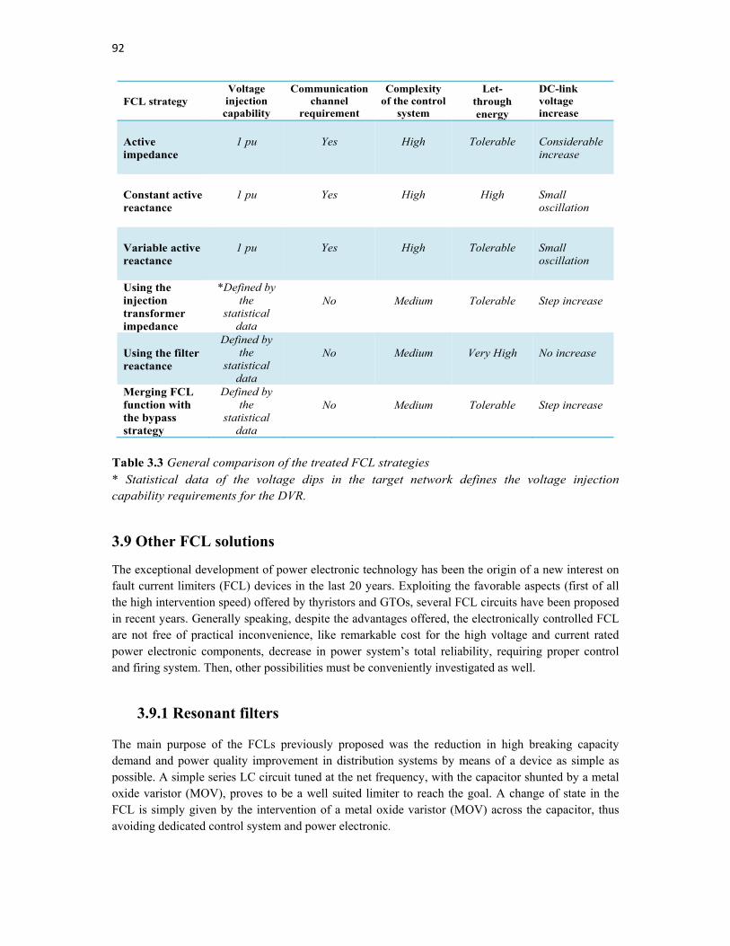
92
FCL strategy
Voltage injection capability
Communication channel
requirement
Complexity of the control
system
Let- through energy
DC-link voltage increase
Active impedance
1 pu
Yes
High
Tolerable
Considerable increase
Constant active reactance
1 pu
Yes
High
High
Small oscillation
Variable active reactance
1 pu
Yes
High
Tolerable
Small oscillation
Using the injection transformer impedance
*Defined by the
statistical data
No
Medium
Tolerable
Step increase
Using the filter reactance
Defined by the
statistical data
No
Medium
Very High
No increase
Merging FCL function with the bypass strategy
Defined by the
statistical data
No
Medium
Tolerable
Step increase
Table 3.3 General comparison of the treated FCL strategies * Statistical data of the voltage dips in the target network defines the voltage injection capability requirements for the DVR.
3.9 Other FCL solutions
The exceptional development of power electronic technology has been the origin of a new interest on fault current limiters (FCL) devices in the last 20 years. Exploiting the favorable aspects (first of all the high intervention speed) offered by thyristors and GTOs, several FCL circuits have been proposed in recent years. Generally speaking, despite the advantages offered, the electronically controlled FCL are not free of practical inconvenience, like remarkable cost for the high voltage and current rated power electronic components, decrease in power system’s total reliability, requiring proper control and firing system. Then, other possibilities must be conveniently investigated as well.
3.9.1 Resonant filters
The main purpose of the FCLs previously proposed was the reduction in high breaking capacity demand and power quality improvement in distribution systems by means of a device as simple as possible. A simple series LC circuit tuned at the net frequency, with the capacitor shunted by a metal oxide varistor (MOV), proves to be a well suited limiter to reach the goal. A change of state in the FCL is simply given by the intervention of a metal oxide varistor (MOV) across the capacitor, thus avoiding dedicated control system and power electronic.
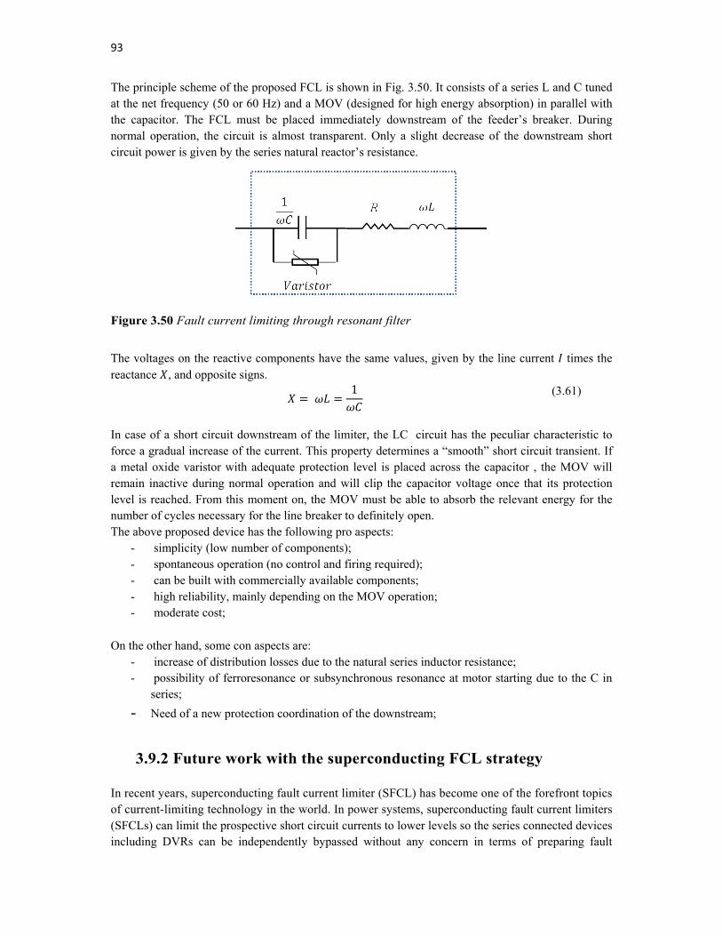
93
The principle scheme of the proposed FCL is shown in Fig. 3.50. It consists of a series L and C tuned at the net frequency (50 or 60 Hz) and a MOV (designed for high energy absorption) in parallel with the capacitor. The FCL must be placed immediately downstream of the feeder’s breaker. During normal operation, the circuit is almost transparent. Only a slight decrease of the downstream short circuit power is given by the series natural reactor’s resistance.
Figure 3.50 Fault current limiting through resonant filter
The voltages on the reactive components have the same values, given by the line current times the reactance , and opposite signs.
1
(3.61)
In case of a short circuit downstream of the limiter, the LC circuit has the peculiar characteristic to force a gradual increase of the current. This property determines a “smooth” short circuit transient. If a metal oxide varistor with adequate protection level is placed across the capacitor , the MOV will remain inactive during normal operation and will clip the capacitor voltage once that its protection level is reached. From this moment on, the MOV must be able to absorb the relevant energy for the number of cycles necessary for the line breaker to definitely open. The above proposed device has the following pro aspects:
- simplicity (low number of components); - spontaneous operation (no control and firing required); - can be built with commercially available components; - high reliability, mainly depending on the MOV operation; - moderate cost;
On the other hand, some con aspects are:
- increase of distribution losses due to the natural series inductor resistance; - possibility of ferroresonance or subsynchronous resonance at motor starting due to the C in
series;
- Need of a new protection coordination of the downstream;
3.9.2 Future work with the superconducting FCL strategy In recent years, superconducting fault current limiter (SFCL) has become one of the forefront topics of current-limiting technology in the world. In power systems, superconducting fault current limiters (SFCLs) can limit the prospective short circuit currents to lower levels so the series connected devices including DVRs can be independently bypassed without any concern in terms of preparing fault

94
current limiting operation for upstream equipment. However in first step a comprehensive analysis of introducing SFCLs on power system stability for targeted network is required.
Figure 3.51 Resistivity – temperature curve of superconductive material Generally speaking Electromagnetic Transient Program (EMTP) simulation results based on a model system show that SFCLs are effective for enhancing the transient stability of electric power systems by restraining the generator rotors from accelerating after faults and improving power quality. Due to low-loss nature in superconducting state during normal operation, SFCLs could offer a solution to controlling fault current levels in utility distribution and transmission networks. In the event of a fault, SFCLs will produce impedances due to losing superconductivity, and insert them into the circuits. Therefore application of SFCLs in electric power systems is expected to suppress the amplitudes of the short circuits currents. In the Fig. 3.51 the main concept of superconductivity is depicted.
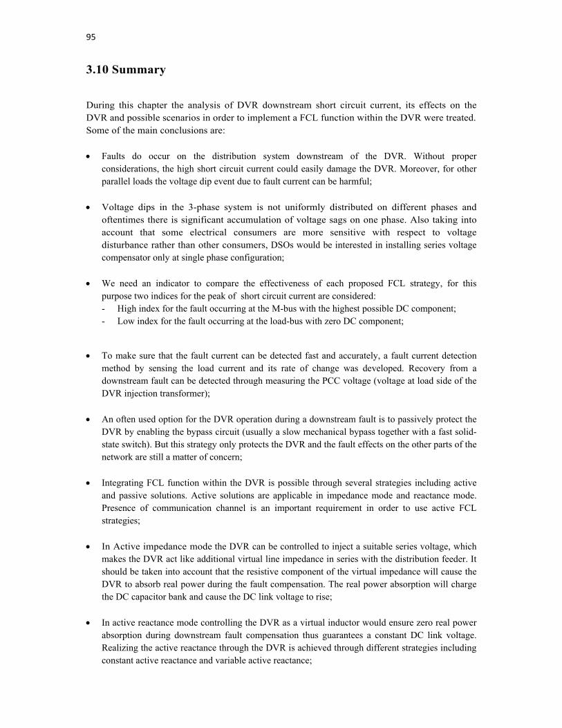
95
3.10 Summary
During this chapter the analysis of DVR downstream short circuit current, its effects on the DVR and possible scenarios in order to implement a FCL function within the DVR were treated. Some of the main conclusions are:
Faults do occur on the distribution system downstream of the DVR. Without proper considerations, the high short circuit current could easily damage the DVR. Moreover, for other parallel loads the voltage dip event due to fault current can be harmful;
Voltage dips in the 3-phase system is not uniformly distributed on different phases and oftentimes there is significant accumulation of voltage sags on one phase. Also taking into account that some electrical consumers are more sensitive with respect to voltage disturbance rather than other consumers, DSOs would be interested in installing series voltage compensator only at single phase configuration;
We need an indicator to compare the effectiveness of each proposed FCL strategy, for this purpose two indices for the peak of short circuit current are considered: - High index for the fault occurring at the M-bus with the highest possible DC component; - Low index for the fault occurring at the load-bus with zero DC component;
To make sure that the fault current can be detected fast and accurately, a fault current detection method by sensing the load current and its rate of change was developed. Recovery from a downstream fault can be detected through measuring the PCC voltage (voltage at load side of the DVR injection transformer);
An often used option for the DVR operation during a downstream fault is to passively protect the DVR by enabling the bypass circuit (usually a slow mechanical bypass together with a fast solid-state switch). But this strategy only protects the DVR and the fault effects on the other parts of the network are still a matter of concern;
Integrating FCL function within the DVR is possible through several strategies including active and passive solutions. Active solutions are applicable in impedance mode and reactance mode. Presence of communication channel is an important requirement in order to use active FCL strategies;
In Active impedance mode the DVR can be controlled to inject a suitable series voltage, which makes the DVR act like additional virtual line impedance in series with the distribution feeder. It should be taken into account that the resistive component of the virtual impedance will cause the DVR to absorb real power during the fault compensation. The real power absorption will charge the DC capacitor bank and cause the DC link voltage to rise;
In active reactance mode controlling the DVR as a virtual inductor would ensure zero real power absorption during downstream fault compensation thus guarantees a constant DC link voltage. Realizing the active reactance through the DVR is achieved through different strategies including constant active reactance and variable active reactance;
96
In the variable active reactance method the reference voltage of the DVR is increased in a ramp waveform instead of step injection. Thanks to this smooth injection, the DC component of short circuit current is less severe but in the transient interval the peak of short circuit current is less limited compared to constant active reactance injection method;
Existence of the communication channel is a main requirement in order to implement active FCL scenarios. The presence and/or reliability of the communication channel is not always achievable or may lead to extra costs. In this condition the solution for implementing FCL function for a DVR is based on employing passive elements including thryristors and inductors in order to limit the short circuit current;
The treated strategies in order to implement the FCL function for a DVR through passive elements include: - Using the impedance of the injection transformer; - Using the filter reactance; - Merging the FCL function with the bypass strategy;
A Comparison of the proposed FCL solutions was treated based on the benchmarks such as: - The DVR voltage injection capability requirement; - Prerequisite of the communication channel; - Let-through energy of the upstream CB; - DC-link voltage increment;
97
Conclusions
Voltage dips have been reported as a major power quality problem. Based upon the chronology of voltage sags we may say that the most voltage dips take place around the 10%–20% voltage level and for a very short time (around 10 cycles). Power electronic controllers for voltage dip mitigation have been discussed and it is concluded that a dynamic voltage restorer is an effective apparatus and economically justified solution to compensate voltage dips.
The main drawback of a DVR is the complexity of protection during downstream fault, because the protection of series connected devices is much more difficult than the protection of shunt devices and a downstream short circuit can be critical and requires extra protection equipment.
An often used option for DVR operation during a downstream fault is to passively protect the DVR by enabling the bypass circuit. The bypass circuit would only protect the DVR during the downstream fault and allows a large fault current to flow in the feeder which could cause upstream bus voltage to drop.
Integrating FCL function within the DVR is possible through several strategies including active and passive solutions. Active solutions are applicable in impedance mode and reactance mode. Presence of communication channel is an important requirement in order to use active FCL strategies. In Active impedance mode the DVR can be controlled to inject a suitable series voltage, which makes the DVR act like additional virtual line impedance in series with the distribution feeder. It should be taken into account that the resistive component of the virtual impedance will cause the DVR to absorb real power during the fault compensation. The real power absorption will charge the DC capacitor bank and cause the DC link voltage to rise. In active reactance mode controlling the DVR as a virtual inductor would ensure zero real power absorption during downstream fault compensation thus guarantees a constant DC link voltage. The presence and/or reliability of the communication channel are not always achievable or may lead to extra costs. Moreover active FCL strategies require 1 pu voltage injection capability.
The analyzed strategies in order to implement the FCL function for a DVR through passive elements include:
1- Using the impedance of the injection transformer: the applied current limitation for the faults occurring immediately after the DVR is not highly effective due to small value of the short circuit impedance of the injection transformer;
2- Using the filter reactance: due to high value of the filter inductance with respect to resistive
part of the faulted circuit the ratio of becomes high which gives rise to slow decaying DC
current component. Therefore using this strategy postpones the first zero crossing of short circuit current and increases the parameter of let-through energy;
3- Merging the FCL function with the bypass strategy: through a relatively small value of dedicated fault current limiting inductance considerable fault current limiting performance is achieved with the possibility of bypassing DVR during small values of short circuit current in order to be detected by the CB. Therefore it seems that this strategy is the promising one in order to implement the FCL function in a DVR with passive elements and without the requirement for communication channel or interference with upstream protection devices;
However sensitivity studies are required in order to generalize the conclusions to other networks.
98
Appendix
A.1 DVR design parameters In [20] and [21] the topic is dedicated to the rating values of a DVR .In Fig A.1 a simplified equivalent circuit of a typical DVR for one phase is illustrated. In the following some concepts regarding the voltage, current and energy rating of a DVR is treated.
Figure A.1: Single-phase simplified model for the DVR.
A.1.1 Voltage, current and energy rating In the simplified model illustrated in Fig. A.1 the DVR consists of a controllable voltage source and a fixed resistance, which is equivalent to the losses in the DVR and a fixed reactance, which is equivalent to the reactive elements in the DVR. The main design parameters for the DVR are the voltage injection capability, the current handling capability and the size of the energy storage. The voltage injection capability can be expressed as:
, %,
100 % (A.1)
The voltage injection capability should be chosen as low as necessary in order to reduce equipment cost and standby losses. Losses tend to increase if the voltage rating of the DVR is increased assuming the current rating of the DVR is fixed and , as the pu value of the resistive voltage drop across the DVR then:
≅ ,
(A.2)
The losses in the DVR can be grouped into losses in the transformer, filter and the converter. The voltage injection is mostly fixed by the requirements to compensate symmetrical and non-symmetrical voltage dips and the next step is to size the current rating of the DVR. Because the DVR is a series connected device, the design of the current handling capability of the DVR depends on:
In-rush phenomenon in the downstream load, such as starting of large motors and magnetization of transformers;
LoadUsupply
- +UconvZsupply
Uload
-
+
Iload-->
Xdvr Rdvr
- +Udvr
99
Non-linear loads, which may lead to higher peak currents;
P and Q characteristics of the downstream loads; Assuming constant load power during voltage dip, the load current may increase according to the remaining voltage at the load bus. Therefore care must be taken if the DVR is supposed to compensate severe voltage dips;
Downstream short circuits; The protection issues are discussed in the next chapter, but the DVR should be able to survive a downstream short circuit and robustness to short circuits may increase the necessary current rating;
Future load increase;
Standby losses; Increasing the current rating of the DVR tends to decrease the standby losses in the system;
Magnetization of the injection transformer; A fast magnetization of a large injection transformers requires a high inrush current, which must be at the same time tolerated by the structure and fed by the VSC;
If the current rating is sized too low, some of the above cases will result in current overload in the VSC and the DVR has to change to bypass mode, in conditions that it is not able to compensate voltage dips. The main parameter to size the current rating of the VSC is the peak current and the RMS current in the grid. The IGBTs have an overload current limit, which will influence the system during short circuit and a heavy loading condition. The sizing of the current handling capability can be defined as:
, %,
100 %
(A.3)
To size voltage, current and energy rating, statistical information about the voltage dip distribution and voltage dip frequency at the location of the inserted DVR is necessary. A one year pre-recording can be necessary to get statistically valid data. By these data it is possible to draw a diagram with the distribution curve of the number of voltage dips as a function of the voltage dip depth and voltage dip duration:
, (A.4)
In Fig.A.2 an example of this curve is given which is reported in [32]. The classification can be complicated if phase jump, symmetry and non-symmetry voltage dips are taken into account. According to what is reported in [68] information about the load is also necessary in the design procedure with the load sensitivity/tripping as a function of the voltage dip depth and voltage dip duration. The CBEMA curve in Fig. 1.2 is one graphical approach to the following function:
, (A.5)
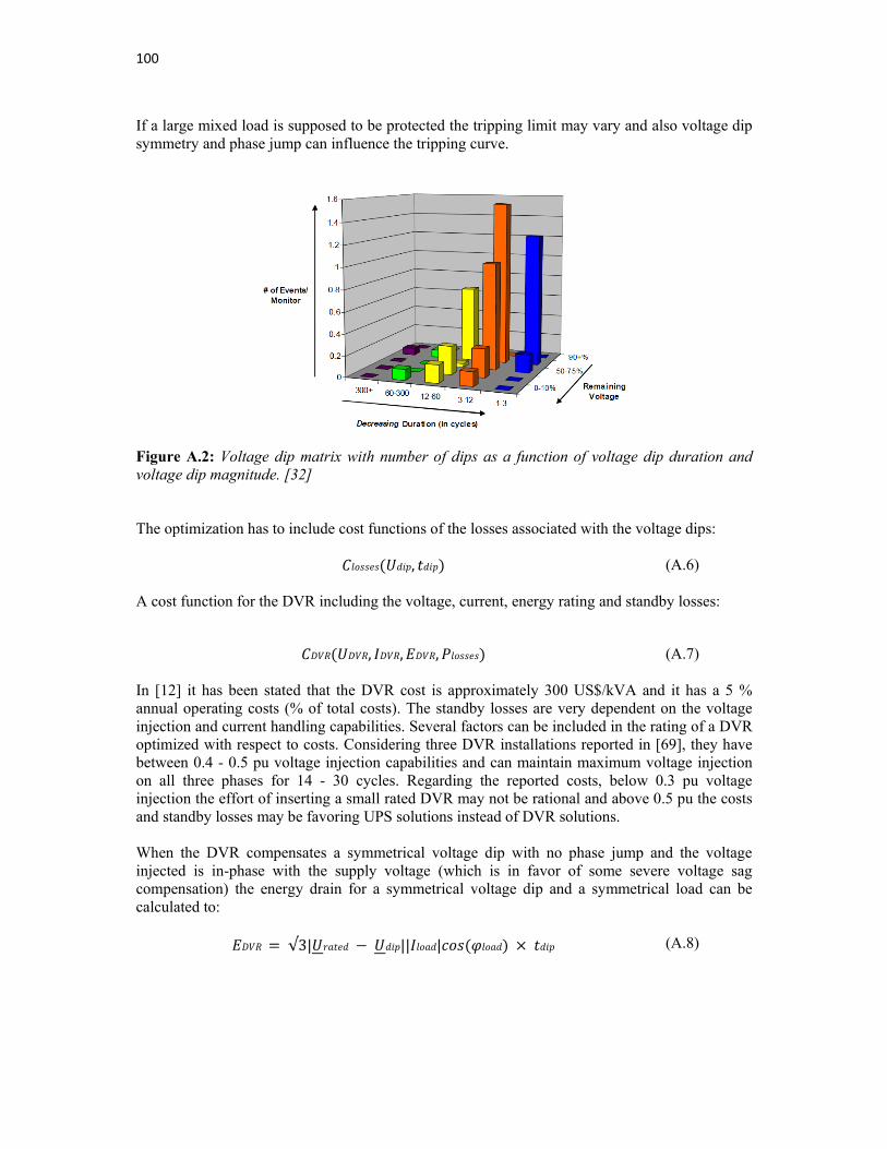
100
If a large mixed load is supposed to be protected the tripping limit may vary and also voltage dip symmetry and phase jump can influence the tripping curve.
Figure A.2: Voltage dip matrix with number of dips as a function of voltage dip duration and voltage dip magnitude. [32] The optimization has to include cost functions of the losses associated with the voltage dips:
, (A.6) A cost function for the DVR including the voltage, current, energy rating and standby losses:
, , , (A.7) In [12] it has been stated that the DVR cost is approximately 300 US$/kVA and it has a 5 % annual operating costs (% of total costs). The standby losses are very dependent on the voltage injection and current handling capabilities. Several factors can be included in the rating of a DVR optimized with respect to costs. Considering three DVR installations reported in [69], they have between 0.4 - 0.5 pu voltage injection capabilities and can maintain maximum voltage injection on all three phases for 14 - 30 cycles. Regarding the reported costs, below 0.3 pu voltage injection the effort of inserting a small rated DVR may not be rational and above 0.5 pu the costs and standby losses may be favoring UPS solutions instead of DVR solutions. When the DVR compensates a symmetrical voltage dip with no phase jump and the voltage injected is in-phase with the supply voltage (which is in favor of some severe voltage sag compensation) the energy drain for a symmetrical voltage dip and a symmetrical load can be calculated to:
√3| || | (A.8)
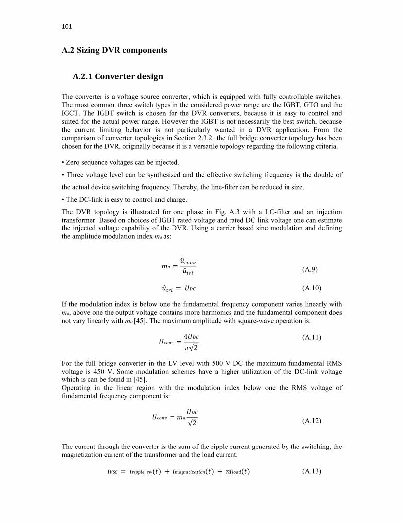
101
A.2 Sizing DVR components
A.2.1Converterdesign The converter is a voltage source converter, which is equipped with fully controllable switches. The most common three switch types in the considered power range are the IGBT, GTO and the IGCT. The IGBT switch is chosen for the DVR converters, because it is easy to control and suited for the actual power range. However the IGBT is not necessarily the best switch, because the current limiting behavior is not particularly wanted in a DVR application. From the comparison of converter topologies in Section 2.3.2 the full bridge converter topology has been chosen for the DVR, originally because it is a versatile topology regarding the following criteria. • Zero sequence voltages can be injected.
• Three voltage level can be synthesized and the effective switching frequency is the double of
the actual device switching frequency. Thereby, the line-filter can be reduced in size.
• The DC-link is easy to control and charge.
The DVR topology is illustrated for one phase in Fig. A.3 with a LC-filter and an injection transformer. Based on choices of IGBT rated voltage and rated DC link voltage one can estimate the injected voltage capability of the DVR. Using a carrier based sine modulation and defining the amplitude modulation index ma as:
(A.9)
(A.10) If the modulation index is below one the fundamental frequency component varies linearly with ma, above one the output voltage contains more harmonics and the fundamental component does not vary linearly with ma [45]. The maximum amplitude with square-wave operation is:
4
√2
(A.11)
For the full bridge converter in the LV level with 500 V DC the maximum fundamental RMS voltage is 450 V. Some modulation schemes have a higher utilization of the DC-link voltage which is can be found in [45]. Operating in the linear region with the modulation index below one the RMS voltage of fundamental frequency component is:
√2
(A.12)
The current through the converter is the sum of the ripple current generated by the switching, the magnetization current of the transformer and the load current.
, (A.13)
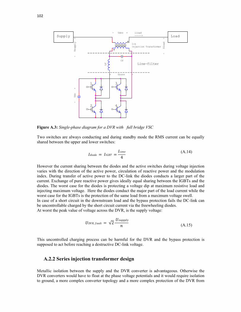
102
Figure A.3: Single-phase diagram for a DVR with full bridge VSC Two switches are always conducting and during standby mode the RMS current can be equally shared between the upper and lower switches:
4
(A.14)
However the current sharing between the diodes and the active switches during voltage injection varies with the direction of the active power, circulation of reactive power and the modulation index. During transfer of active power to the DC-link the diodes conducts a larger part of the current. Exchange of pure reactive power gives ideally equal sharing between the IGBTs and the diodes. The worst case for the diodes is protecting a voltage dip at maximum resistive load and injecting maximum voltage. Here the diodes conduct the major part of the load current while the worst case for the IGBTs is the protection of the same load from a maximum voltage swell. In case of a short circuit in the downstream load and the bypass protection fails the DC-link can be uncontrollable charged by the short circuit current via the freewheeling diodes. At worst the peak value of voltage across the DVR, is the supply voltage:
, √2
(A.15)
This uncontrolled charging process can be harmful for the DVR and the bypass protection is supposed to act before reaching a destructive DC-link voltage.
A.2.2 Series injection transformer design Metallic isolation between the supply and the DVR converter is advantageous. Otherwise the DVR converters would have to float at the phase voltage potentials and it would require isolation to ground, a more complex converter topology and a more complex protection of the DVR from
Cf
-
Udc
+
Lf
.
.
- Udvr +
Supply Load
-------------------------
-------------------------
Line-filter
+ Uconv -
4
3
2
1
----->iload
- Us
upply
+
-
Uloa
d +
1:nInjection Transformer
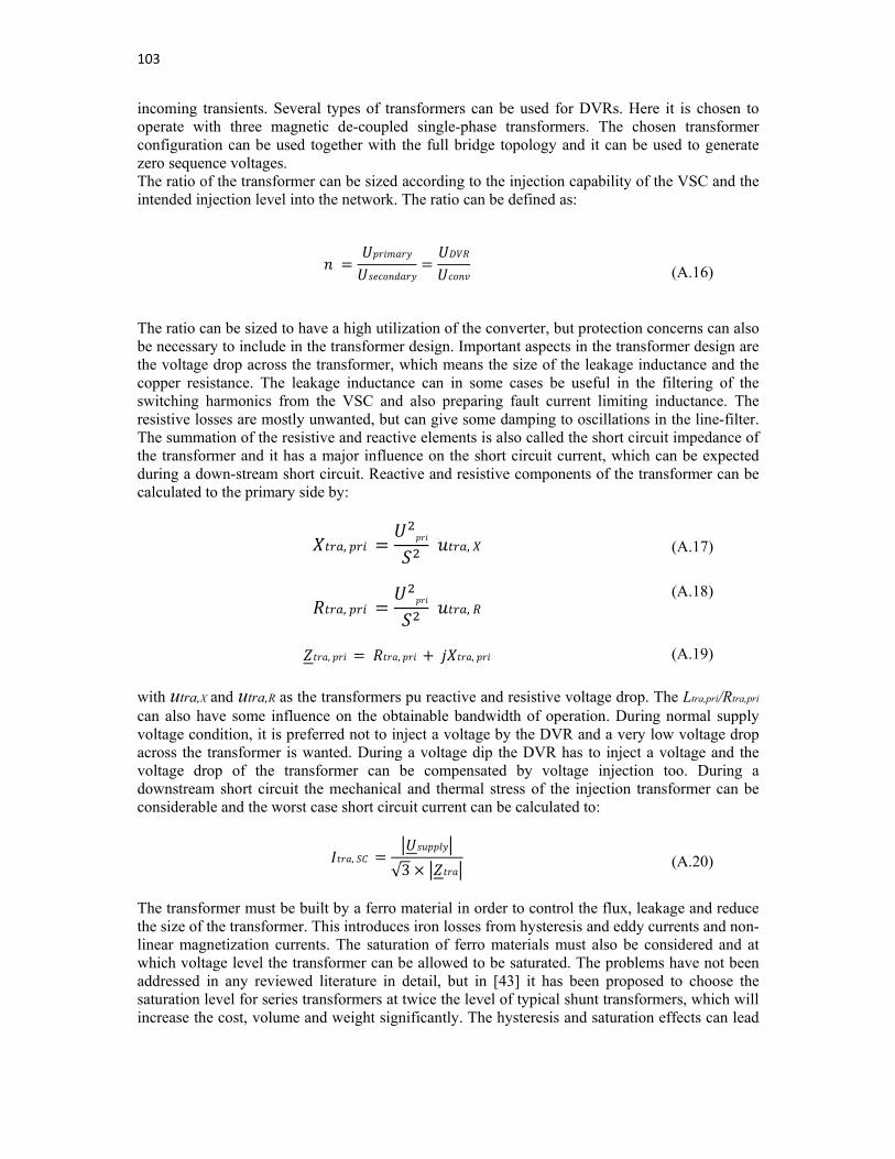
103
incoming transients. Several types of transformers can be used for DVRs. Here it is chosen to operate with three magnetic de-coupled single-phase transformers. The chosen transformer configuration can be used together with the full bridge topology and it can be used to generate zero sequence voltages. The ratio of the transformer can be sized according to the injection capability of the VSC and the intended injection level into the network. The ratio can be defined as:
(A.16)
The ratio can be sized to have a high utilization of the converter, but protection concerns can also be necessary to include in the transformer design. Important aspects in the transformer design are the voltage drop across the transformer, which means the size of the leakage inductance and the copper resistance. The leakage inductance can in some cases be useful in the filtering of the switching harmonics from the VSC and also preparing fault current limiting inductance. The resistive losses are mostly unwanted, but can give some damping to oscillations in the line-filter. The summation of the resistive and reactive elements is also called the short circuit impedance of the transformer and it has a major influence on the short circuit current, which can be expected during a down-stream short circuit. Reactive and resistive components of the transformer can be calculated to the primary side by:
, ,
(A.17)
, , (A.18)
, , ,
(A.19)
with utra,X and utra,R as the transformers pu reactive and resistive voltage drop. The Ltra,pri/Rtra,pri
can also have some influence on the obtainable bandwidth of operation. During normal supply voltage condition, it is preferred not to inject a voltage by the DVR and a very low voltage drop across the transformer is wanted. During a voltage dip the DVR has to inject a voltage and the voltage drop of the transformer can be compensated by voltage injection too. During a downstream short circuit the mechanical and thermal stress of the injection transformer can be considerable and the worst case short circuit current can be calculated to:
,√3
(A.20)
The transformer must be built by a ferro material in order to control the flux, leakage and reduce the size of the transformer. This introduces iron losses from hysteresis and eddy currents and non-linear magnetization currents. The saturation of ferro materials must also be considered and at which voltage level the transformer can be allowed to be saturated. The problems have not been addressed in any reviewed literature in detail, but in [43] it has been proposed to choose the saturation level for series transformers at twice the level of typical shunt transformers, which will increase the cost, volume and weight significantly. The hysteresis and saturation effects can lead
104
to high in-rush currents, which must be supplied by the DVR. The in-rush occurs, when it changes from zero voltage injection to high voltage injection. The transformer floats at the supply voltage level and the isolation level has to be accordingly high with uniform isolation. Capacitive effects in the transformer should be considered because capacitive coupling between the primary and secondary winding is present.
A.2.3 Filter design Design of a line-filter for a DVR has been treated in [24]. The filter is inserted to damp the switching harmonics generated by the PWM control of VSC. The PWM control generates harmonics and if the modulation index is kept below one the switching harmonics are typically centered on the switching frequency and multiples of the switching frequency. Consumer products have to keep certain standards before released to mass distribution. Regarding EMC two important areas are usually included [70]:
1. Conducted emission in the frequency region 150 kHz - 30 MHz;
2. Radiated emission in 30 MHz -1 GHz;
Even though a large part of the harmonics is injected in the spectrum without any limits 2 kHz - 150 kHz still it is considered important to damp the switching harmonics in order to be able to fulfill standards in conducted emission in the region 150 kHz - 30 MHz and radiated emission in the 30 MHz - 1 GHz. Due to the fact that the DVR is not a consumer product and it is a series connected device to be placed in the distribution system thereby it cannot be classified as a typical load. So the criteria to design the filter to follow certain standards seem complex because the DVR is difficult to classify within existing classes in the standards. The filter design deals with guidelines to size the filter parameters and the consequences for the DVR performance. Ideally, the PWM converter only injects a fundamental component and the switching harmonics assuming the converter is operated in the linear modulation region. A variety of factors can lead to the injection of non-characteristic harmonics. Some of the factors are:
Non-linear effects in the converter caused by the non-linear voltage drop, turn on, turn-
off delay and dead time;
Quantification in the A/D conversion and the duty cycle generation;
Aliasing in the A/D conversion;
Omission of short duty cycles strategy to reduce switching losses;
Background harmonic distortion from the grid enters the control and leads to an injection of harmonics in the system;
Non-linear control algorithms;
The injected harmonic currents can be substantial, if it is a shunt connected PWM inverter operated against a strong supply connection. Regarding the DVR, the non-fundamental DVR voltages will be injected in series with the supply and the load therefore the associated injected currents depend on the supply and load impedance. The load impedances are assumed to be relatively high. The non-fundamental harmonic voltages will still be injected and cause an increased total harmonic distortion of the load voltage. The emission of noise from shunt devices is less complicated in comparison with series devices. In Fig. A.4a the model for a shunt device is
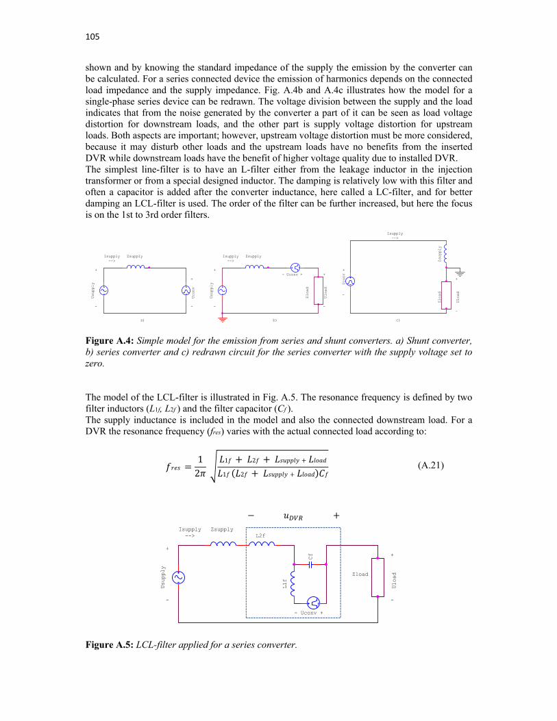
105
shown and by knowing the standard impedance of the supply the emission by the converter can be calculated. For a series connected device the emission of harmonics depends on the connected load impedance and the supply impedance. Fig. A.4b and A.4c illustrates how the model for a single-phase series device can be redrawn. The voltage division between the supply and the load indicates that from the noise generated by the converter a part of it can be seen as load voltage distortion for downstream loads, and the other part is supply voltage distortion for upstream loads. Both aspects are important; however, upstream voltage distortion must be more considered, because it may disturb other loads and the upstream loads have no benefits from the inserted DVR while downstream loads have the benefit of higher voltage quality due to installed DVR. The simplest line-filter is to have an L-filter either from the leakage inductor in the injection transformer or from a special designed inductor. The damping is relatively low with this filter and often a capacitor is added after the converter inductance, here called a LC-filter, and for better damping an LCL-filter is used. The order of the filter can be further increased, but here the focus is on the 1st to 3rd order filters.
Figure A.4: Simple model for the emission from series and shunt converters. a) Shunt converter, b) series converter and c) redrawn circuit for the series converter with the supply voltage set to zero. The model of the LCL-filter is illustrated in Fig. A.5. The resonance frequency is defined by two filter inductors (L1f, L2f ) and the filter capacitor (Cf ). The supply inductance is included in the model and also the connected downstream load. For a DVR the resonance frequency (fres) varies with the actual connected load according to:
12
1 2
1 2
(A.21)
Figure A.5: LCL-filter applied for a series converter.
Uconv +-
-
+
Uconv
-->Isupply
Usuppl
y
+
Zsupply
-
Uconv
-
+
-
+
Uloa
d
Zsup
ply
-->Isupply
Zloa
d
-
+
Uload
Usuppl
y
-->Isupply Zsupply
-
+
Zload
a) b) c)
Uconv +-
-
+
Uloa
d
Usup
ply
-->Isupply Zsupply
-
+
Udvr-
Zload
+
Cf
L2f
L1f
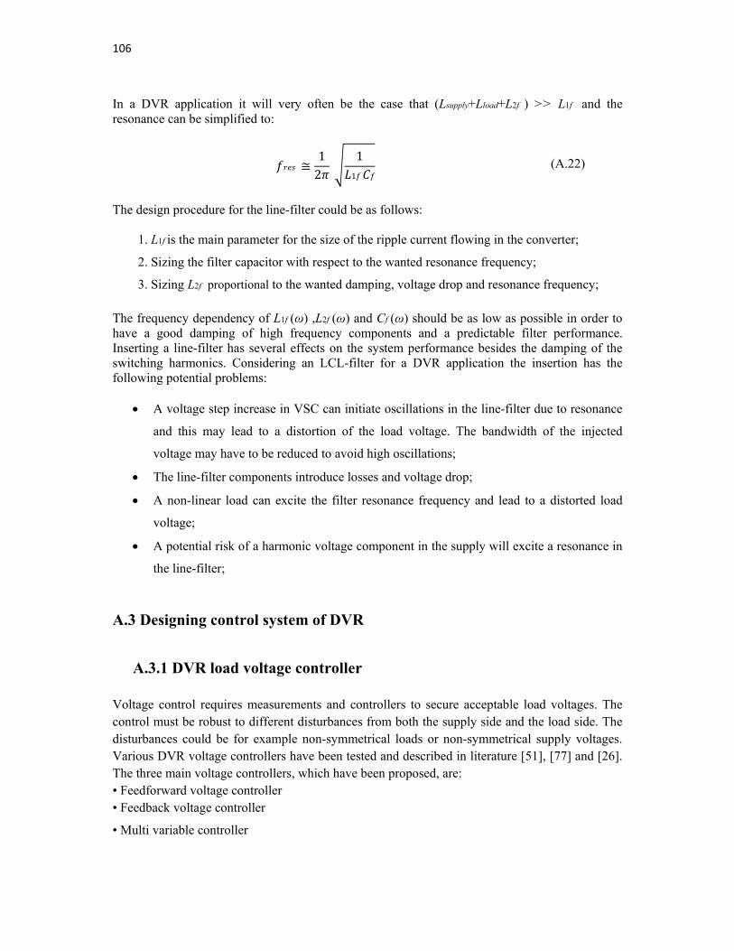
106
In a DVR application it will very often be the case that (Lsupply+Lload+L2f ) >> L1f and the resonance can be simplified to:
≅12
11
(A.22)
The design procedure for the line-filter could be as follows:
1. L1f is the main parameter for the size of the ripple current flowing in the converter;
2. Sizing the filter capacitor with respect to the wanted resonance frequency;
3. Sizing L2f proportional to the wanted damping, voltage drop and resonance frequency;
The frequency dependency of L1f (ω) ,L2f (ω) and Cf (ω) should be as low as possible in order to have a good damping of high frequency components and a predictable filter performance. Inserting a line-filter has several effects on the system performance besides the damping of the switching harmonics. Considering an LCL-filter for a DVR application the insertion has the following potential problems:
A voltage step increase in VSC can initiate oscillations in the line-filter due to resonance
and this may lead to a distortion of the load voltage. The bandwidth of the injected
voltage may have to be reduced to avoid high oscillations;
The line-filter components introduce losses and voltage drop;
A non-linear load can excite the filter resonance frequency and lead to a distorted load
voltage;
A potential risk of a harmonic voltage component in the supply will excite a resonance in
the line-filter;
A.3 Designing control system of DVR
A.3.1 DVR load voltage controller Voltage control requires measurements and controllers to secure acceptable load voltages. The control must be robust to different disturbances from both the supply side and the load side. The disturbances could be for example non-symmetrical loads or non-symmetrical supply voltages. Various DVR voltage controllers have been tested and described in literature [51], [77] and [26]. The three main voltage controllers, which have been proposed, are: • Feedforward voltage controller • Feedback voltage controller
• Multi variable controller
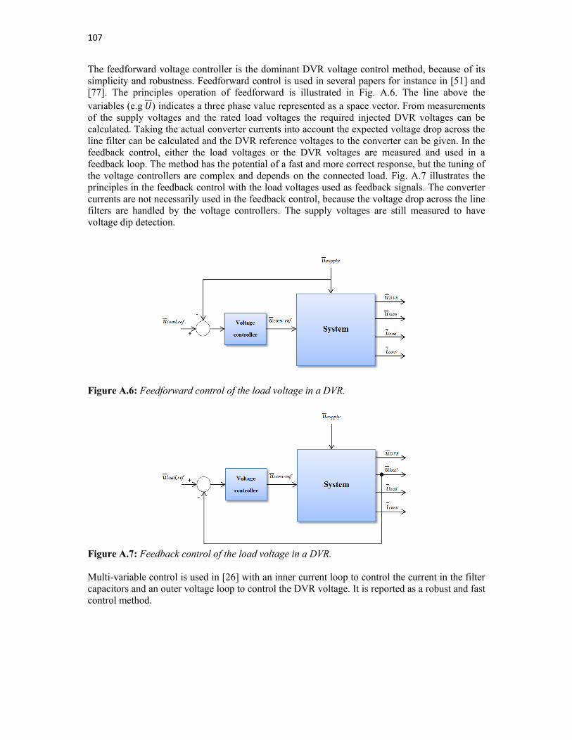
107
The feedforward voltage controller is the dominant DVR voltage control method, because of its simplicity and robustness. Feedforward control is used in several papers for instance in [51] and [77]. The principles operation of feedforward is illustrated in Fig. A.6. The line above the variables (e.g ) indicates a three phase value represented as a space vector. From measurements of the supply voltages and the rated load voltages the required injected DVR voltages can be calculated. Taking the actual converter currents into account the expected voltage drop across the line filter can be calculated and the DVR reference voltages to the converter can be given. In the feedback control, either the load voltages or the DVR voltages are measured and used in a feedback loop. The method has the potential of a fast and more correct response, but the tuning of the voltage controllers are complex and depends on the connected load. Fig. A.7 illustrates the principles in the feedback control with the load voltages used as feedback signals. The converter currents are not necessarily used in the feedback control, because the voltage drop across the line filters are handled by the voltage controllers. The supply voltages are still measured to have voltage dip detection.
Figure A.6: Feedforward control of the load voltage in a DVR.
Figure A.7: Feedback control of the load voltage in a DVR. Multi-variable control is used in [26] with an inner current loop to control the current in the filter capacitors and an outer voltage loop to control the DVR voltage. It is reported as a robust and fast control method.
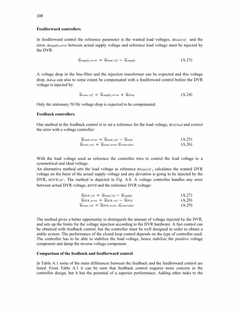
108
Feedforward controllers In feedforward control the reference parameter is the wanted load voltages, uload,ref, and the error, usupply,error between actual supply voltage and reference load voltage must be injected by the DVR:
, , (A.23)
A voltage drop in the line-filter and the injection transformer can be expected and this voltage drop, udrop can also to some extent be compensated with a feedforward control before the DVR voltage is injected by:
, , (A.24) Only the stationary 50 Hz voltage drop is expected to be compensated. Feedback controllers One method in the feedback control is to set a reference for the load voltage, uref,load and correct the error with a voltage controller:
, , (A.25) , , . (A.26)
With the load voltage used as reference the controller tries to control the load voltage to a symmetrical and ideal voltage. An alternative method sets the load voltage as reference uload,ref , calculates the wanted DVR voltage on the basis of the actual supply voltage and any deviation is going to be injected by the DVR, uDVR,ref . The method is depicted in Fig. A.8. A voltage controller handles any error between actual DVR voltage, uDVR and the reference DVR voltage:
, , (A.27) , , (A.28) , , . (A.29)
The method gives a better opportunity to distinguish the amount of voltage injected by the DVR, and sets up the limits for the voltage injection according to the DVR hardware. A fast control can be obtained with feedback control, but the controller must be well designed in order to obtain a stable system. The performance of the closed loop control depends on the type of controller used. The controller has to be able to stabilize the load voltage, hence stabilize the positive voltage component and damp the inverse voltage component. Comparison of the feedback and feedforward control In Table A.1 some of the main differences between the feedback and the feedforward control are listed. From Table A.1 it can be seen that feedback control requires more concern in the controller design, but it has the potential of a superior performance. Adding other tasks to the
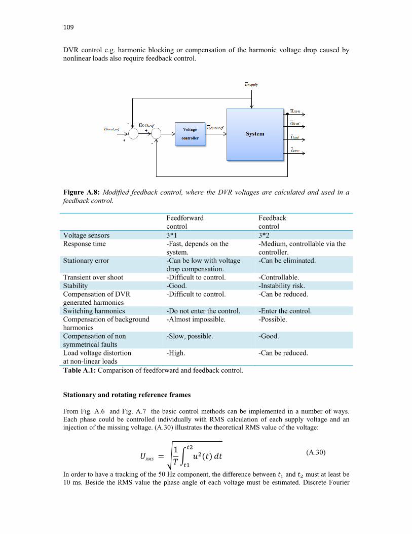
109
DVR control e.g. harmonic blocking or compensation of the harmonic voltage drop caused by nonlinear loads also require feedback control.
Figure A.8: Modified feedback control, where the DVR voltages are calculated and used in a feedback control. Feedforward
control Feedback control
Voltage sensors 3*1 3*2 Response time -Fast, depends on the
system. -Medium, controllable via the controller.
Stationary error -Can be low with voltage drop compensation.
-Can be eliminated.
Transient over shoot -Difficult to control. -Controllable. Stability -Good. -Instability risk. Compensation of DVR generated harmonics
-Difficult to control. -Can be reduced.
Switching harmonics -Do not enter the control. -Enter the control. Compensation of background harmonics
-Almost impossible. -Possible.
Compensation of non symmetrical faults
-Slow, possible. -Good.
Load voltage distortion at non-linear loads
-High. -Can be reduced.
Table A.1: Comparison of feedforward and feedback control.
Stationary and rotating reference frames From Fig. A.6 and Fig. A.7 the basic control methods can be implemented in a number of ways. Each phase could be controlled individually with RMS calculation of each supply voltage and an injection of the missing voltage. (A.30) illustrates the theoretical RMS value of the voltage:
1
(A.30)
In order to have a tracking of the 50 Hz component, the difference between and must at least be 10 ms. Beside the RMS value the phase angle of each voltage must be estimated. Discrete Fourier
110
Transformation (DFT) can also be used to detect the fundamental 50 Hz component and the associated phase angle. The method is slow and requires a large amount of data processing. (A.31) illustrates the DFT method.
2
, 0 1 (A.31)
N is the size of the data array and a calculation of one element requires (N-1) complex multiplications and (N-1) complex additions. Using DFT is time consuming and difficult to implement in real time control. A high bandwidth is required to protect very sensitive loads, and therefore only instantaneous compensation and detection methods of voltage dips are further considered. The control of the fundamental voltages is done in the time domain. The frequency domain processing can be used in some cases for harmonic blocking, which could be a secondary task for the DVR. The voltage control is often implemented in different reference frames. The purpose of using another reference system is to simplify the control or improve the performance. The typically used reference frames are: • Stationary reference frames
– Three-phase system (RST)
– Space vector system (αβ0)
• Rotating reference frames
– Synchronous rotating system (dq0)
– Inverse rotating system (-dq0)
In the stationary RST reference frames the current and voltages are sinusoidal quantities. A transformation of the RST-system to a space vector representation can often be advantageous. The transformation is:
23
2 3 4 3 (A.32)
Rewriting in matrix representation, the matrix can be written as:
231 0.5 0.50 √3/2 √3/2
(A.33)
Zero sequence values are eliminated and with symmetrical phase voltages the resulting space vector rotates with a constant angular velocity and it has a constant magnitude. Transformation to a rotating system can often lead to further simplifications and improvements of the control system. The transformation to a rotating dq-frame is shown in:
(A.34)
The transformation matrix can be written as:
(A.35)
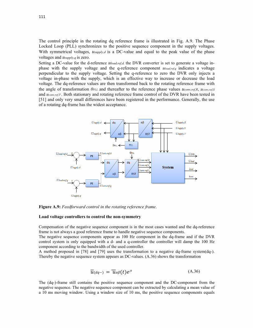
111
The control principle in the rotating dq reference frame is illustrated in Fig. A.9. The Phase Locked Loop (PLL) synchronizes to the positive sequence component in the supply voltages. With symmetrical voltages, usupply,d is a DC-value and equal to the peak value of the phase voltages and usupply,q is zero. Setting a DC-value for the d-reference uload,ref,d, the DVR converter is set to generate a voltage in-phase with the supply voltage and the q-reference component uload,ref,q indicates a voltage perpendicular to the supply voltage. Setting the q-reference to zero the DVR only injects a voltage in-phase with the supply, which is an effective way to increase or decrease the load voltage. The dq-reference values are then transformed back to the rotating reference frame with the angle of transformation θPLL and thereafter to the reference phase values uconv,ref,R, uconv,ref,S
and uconv,ref,T . Both stationary and rotating reference frame control of the DVR have been tested in [51] and only very small differences have been registered in the performance. Generally, the use of a rotating dq-frame has the widest acceptance.
Figure A.9: Feedforward control in the rotating reference frame.
Load voltage controllers to control the non-symmetry Compensation of the negative sequence component is in the most cases wanted and the dq-reference frame is not always a good reference frame to handle negative sequence components. The negative sequence components appear as 100 Hz component in the dq-frame and if the DVR control system is only equipped with a d- and a q-controller the controller will damp the 100 Hz component according to the bandwidth of the used controller. A method proposed in [78] and [79] uses the transformation to a negative dq-frame system(dq-). Thereby the negative sequence system appears as DC-values. (A.36) shows the transformation
(A.36) The (dq-)-frame still contains the positive sequence component and the DC-component from the negative sequence. The negative sequence component can be extracted by calculating a mean value of a 10 ms moving window. Using a window size of 10 ms, the positive sequence components equals
112
zero in mean value. The mean value in the (dq-)-system, must be calculated both for the d- and q-component, according to:
,1 (A.37)
,1
(A.38)
Calculation of the mean value in a DSP requires storing of data. For instance in the case of a sampling frequency equal to 5 kHz an array of 50 elements must be stored:
10 50 (A.39) Practical calculations of the mean value can be done by adding the new value, u(n) and subtracting the oldest value u(n-50) to a sum, usum. Thereafter the mean value can be calculated:
50 (A.40) 1
(A.41)
Also instead of mean value the DC-value may be extracted by filtering technics, which for low order filters require less storage of data. The extracted result of the negative sequence component can be used for reducing non-symmetry in the load voltage. Both feedback and feedforward control of the negative sequence component can be used. The reference value of the negative sequence component, u(dq−),ref is most likely set to zero in order to have symmetrical load voltages. The compensation of the negative component with a dedicated control setup is much slower compared with the positive sequence controller. The time constant of a feedforward control is in the order 5 - 10 ms before the DVR effectively can compensate for the non-symmetrical voltage. For both feedforward and feedback methods this (dq-)-transformation appear to be the most promising method to separately control positive and negative sequence components.
A.3.2 DVR DC-link voltage controllers So far the control of the AC voltages across the DVR has been analyzed. In this section different methods to control the DC-link voltage are described. The DC-link voltage can to some degree be controlled by the series DVR converter. In [80] the DVR converter is used to charge the DC-link and the attached batteries, but often the DC voltage is controlled by an externally DC-link charger. Some DVR system topologies give the opportunity to control the DC-link voltage while in other topologies DC-link voltage is relatively uncontrollable. In some DVR configurations the DC-link voltage can be chosen to be kept constant at all times. With a constant DC-link voltage the generated DVR voltage can always be at maximum. During a voltage dip the rating of the DC-link charger may give limitations in the ability to maintain a constant DC-link voltage. The two main topologies, which are capable of maintaining a constant DC voltage, are a DVR with an active shunt converter (AC/DC converter) or a topology with separate energy storage and a DC-link equipped with DC/DC converter. Another simpler charger could be a diode charger connected to the
113
supply side or to the load side of the series converter and the DC-link voltage depends on the supply or the load voltages. In order to control the DC-link voltage a voltage drop across the DVR has to be controlled to take power from the supply to charge the DC-link voltage. The load voltage is a summation of the supply and the DVR voltage:
(A.42) The DVR voltage is equal to the generated converter voltage (Uconv) subtracted line-filter voltage drop.
(A.43) To be able to charge the DC-link the injected converter voltage must include a charging voltage drop, which corresponds to a resistive voltage drop across the DVR. In order to control the load voltages to rated values the DVR can circulate reactive power. The ability to take active power from the grid and still maintain a rated load voltage depends on the grid strength, the supply voltage level, resistive and inductive voltage drop caused by the line-filter and finally the apparent power absorbed by the load,
√3 (A.44)
A current has to flow to the load in order to be able to charge the DC-link and the charging voltage is always in-phase with the load current. During low load currents the charging voltage has to be increased to ensure a fast charging. In this condition the voltage drops across the line-filter and supply line are also low and a higher charging voltage can be accepted.
A.3.3 DVR Voltage dip detector An essential part of the DVR control system is the detection circuit. A voltage dip must be detected fast and corrected with a minimum of false operations. The detection circuit operates the DVR from standby to active mode and vice versa. Parameters for the detection circuit are: • Robust operation with the presence of background voltage quality problems.
• Fast voltage dip detection and transition to active operation to minimize load under voltages.
• Detection of a restored supply voltage and transition from active to standby operation and a
minimization of load over-voltages.
These are the main parameters to the detection circuit. To achieve a fast detection it is possible to use instantaneously measurements instead of RMS based calculations which introduce delay to the dip detector. The measurements of the supply voltage gives the instantaneously voltage and the transformation of the supply voltages to a rotating or a stationary reference can in some cases be advantageously. Three voltage dip detection methods are here presented: 1. Magnitude of the space vector in αβ-reference
| , | , , (A.45)
| , | (A.46)

114
2. Length of the d-component and q-component in the dq-reference frame comparing each value with threshold values.
, (A.47) , or , (A.48)
3. Length of the error vector comparing with a threshold value.
| , | , , , , (A.49)
| , | (A.50) The detection circuit depends on the DVR hardware and control strategy. All the three methods can detect a large symmetrical voltage dip without any phase jump. A non-symmetrical voltage dip on the other hand can give some problems in the detection. The voltage dip can often give the appearance that the supply voltages are restored. Fig. A.10a illustrates a very typically non symmetrical voltage dip. The dashed line indicates the non-faulted voltages and the solid line the faulted voltages. At t = 10 ms the instantaneous values are equal in the faulted and the non-faulted case even though the fault still persists. Fig. A.10b-d illustrates how the three different methods detect this type of fault. At t = 11.7 ms the d-component has reduced to 90 % of the rated value in Fig. A.10c and the error in Fig. A.10d is above 10 %. The case illustrates that the detection of a small non-symmetrical voltage dip can be delayed and the delay depends on the occurrence time of non-symmetrical voltage dip and also the type of it. All the methods are equally effective in the detection of this type of non-symmetrical fault. If the voltage dip contains a phase jump method 1 will only detect the voltage reduction, but not the phase jump. In the methods 2 and 3 a phase jump will lead to a reduction in both the d- and q-component. For that case detection method number 3 seems better, because it gives the ability to detect phase jump and only one parameter has to be compared.
Figure A.10: Detection of a non-symmetrical voltage dip. a) RST-system with the faulted and non-faulted voltages (dashed), b) method 1 amplitude of the space vector, c) method 2 evaluation of the d- and q-component and d) method 3, the magnitude of the error vector.
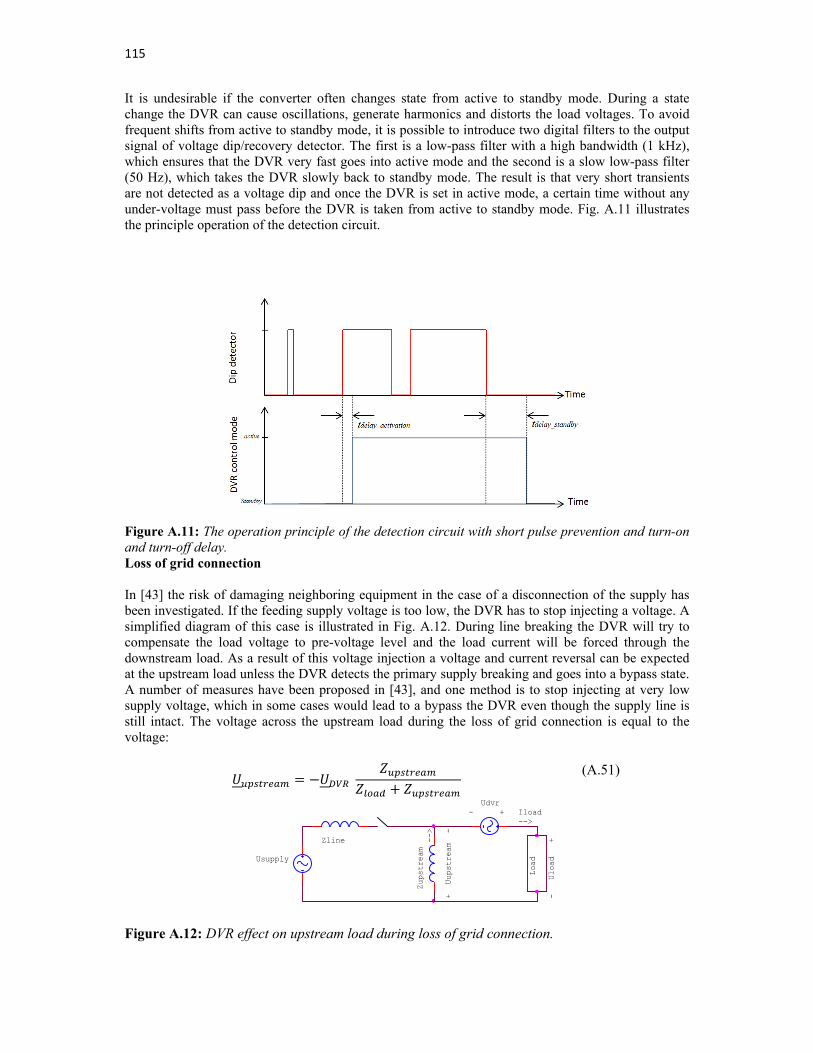
115
It is undesirable if the converter often changes state from active to standby mode. During a state change the DVR can cause oscillations, generate harmonics and distorts the load voltages. To avoid frequent shifts from active to standby mode, it is possible to introduce two digital filters to the output signal of voltage dip/recovery detector. The first is a low-pass filter with a high bandwidth (1 kHz), which ensures that the DVR very fast goes into active mode and the second is a slow low-pass filter (50 Hz), which takes the DVR slowly back to standby mode. The result is that very short transients are not detected as a voltage dip and once the DVR is set in active mode, a certain time without any under-voltage must pass before the DVR is taken from active to standby mode. Fig. A.11 illustrates the principle operation of the detection circuit.
Figure A.11: The operation principle of the detection circuit with short pulse prevention and turn-on and turn-off delay. Loss of grid connection In [43] the risk of damaging neighboring equipment in the case of a disconnection of the supply has been investigated. If the feeding supply voltage is too low, the DVR has to stop injecting a voltage. A simplified diagram of this case is illustrated in Fig. A.12. During line breaking the DVR will try to compensate the load voltage to pre-voltage level and the load current will be forced through the downstream load. As a result of this voltage injection a voltage and current reversal can be expected at the upstream load unless the DVR detects the primary supply breaking and goes into a bypass state. A number of measures have been proposed in [43], and one method is to stop injecting at very low supply voltage, which in some cases would lead to a bypass the DVR even though the supply line is still intact. The voltage across the upstream load during the loss of grid connection is equal to the voltage:
(A.51)
Figure A.12: DVR effect on upstream load during loss of grid connection.
Zupstream
+ U
upstream -
-->Iload
-->
LoadUsupply
+Udvr
Zline
-
-
Uload +
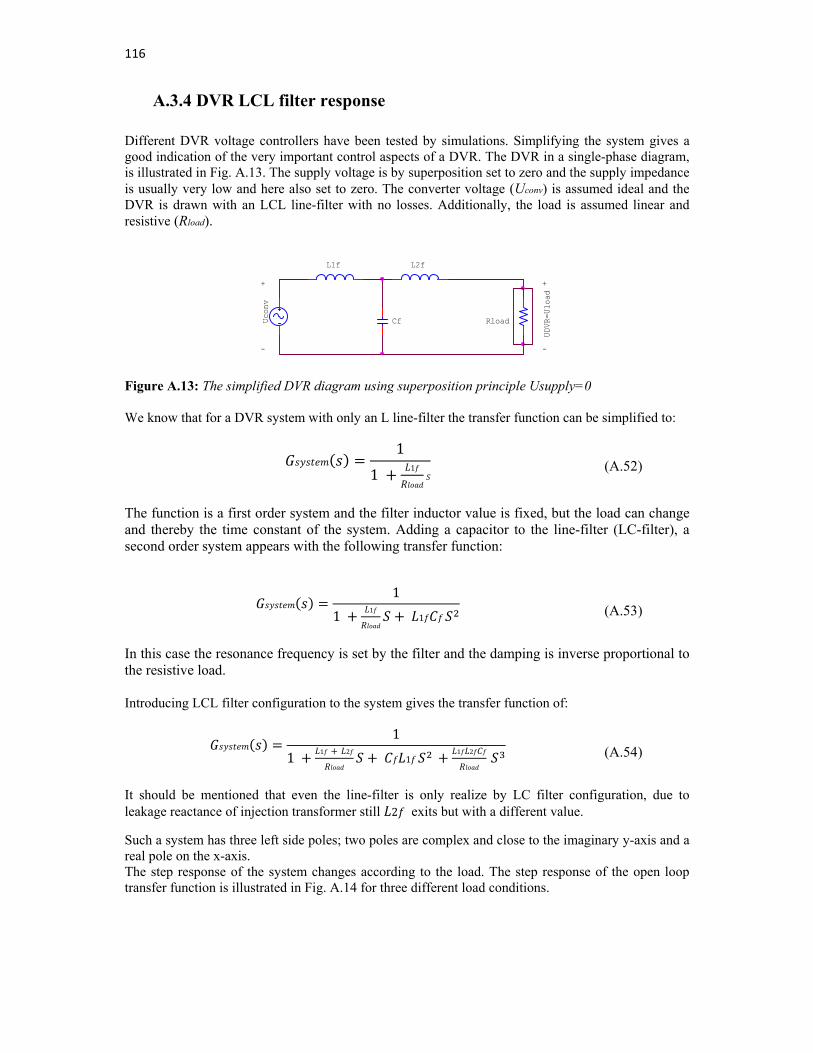
116
A.3.4 DVR LCL filter response Different DVR voltage controllers have been tested by simulations. Simplifying the system gives a good indication of the very important control aspects of a DVR. The DVR in a single-phase diagram, is illustrated in Fig. A.13. The supply voltage is by superposition set to zero and the supply impedance is usually very low and here also set to zero. The converter voltage (Uconv) is assumed ideal and the DVR is drawn with an LCL line-filter with no losses. Additionally, the load is assumed linear and resistive (Rload).
Figure A.13: The simplified DVR diagram using superposition principle Usupply=0 We know that for a DVR system with only an L line-filter the transfer function can be simplified to:
1
11
(A.52)
The function is a first order system and the filter inductor value is fixed, but the load can change and thereby the time constant of the system. Adding a capacitor to the line-filter (LC-filter), a second order system appears with the following transfer function:
1
11
1
(A.53)
In this case the resonance frequency is set by the filter and the damping is inverse proportional to the resistive load. Introducing LCL filter configuration to the system gives the transfer function of:
1
11 2
1 1 2
(A.54)
It should be mentioned that even the line-filter is only realize by LC filter configuration, due to leakage reactance of injection transformer still 2 exits but with a different value.
Such a system has three left side poles; two poles are complex and close to the imaginary y-axis and a real pole on the x-axis. The step response of the system changes according to the load. The step response of the open loop transfer function is illustrated in Fig. A.14 for three different load conditions.
-
Rload
L1f L2f
CfUconv
+
-
UDVR=U
load
+
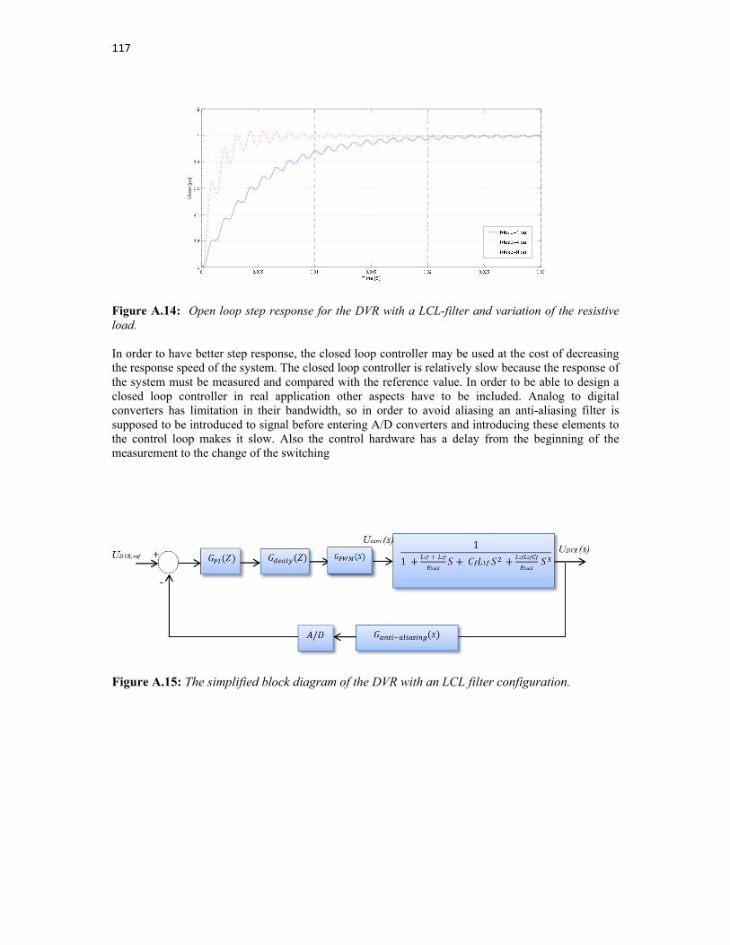
117
Figure A.14: Open loop step response for the DVR with a LCL-filter and variation of the resistive load. In order to have better step response, the closed loop controller may be used at the cost of decreasing the response speed of the system. The closed loop controller is relatively slow because the response of the system must be measured and compared with the reference value. In order to be able to design a closed loop controller in real application other aspects have to be included. Analog to digital converters has limitation in their bandwidth, so in order to avoid aliasing an anti-aliasing filter is supposed to be introduced to signal before entering A/D converters and introducing these elements to the control loop makes it slow. Also the control hardware has a delay from the beginning of the measurement to the change of the switching
Figure A.15: The simplified block diagram of the DVR with an LCL filter configuration.
Ulo
ad [
pu]

118
References [1] D.S. Dorr. “Point of Utilization Power Quality Study Results” IEEE Transactions on Industry Application, Vol. 31, No. 4, pp. 658 - 666, 1995.
[2] J.J. Stanislawski. “National Power Laboratory Power Quality Study 1972 to 1979 Revisited” 17th International Telecommunications Energy Conference INTELEC′95, pp. 544 - 551, 1995.
[3] Igor Amariz Pires, Filipe Dias de Oliveira, Sidelmo Magalhaes Silva, and Braz de Jesus Cardoso Filho, “On the Application of Single-Phase Voltage Sag Compensators in Three-Phase Systems” IEEE TRANSACTIONS ON INDUSTRY APPLICATIONS, VOL. 53, NO. 1, JANUARY/FEBRUARY 2017
[4] F. Carlsson, C. Sadarangani, and B.Widell, “Impacts of voltage sags on a blast furnace process,” in Proc. CIGRE Symp., Stockholm, Sweden, 2001.
[5] F. Carlsson, B. Widell, and C. Sadarangani. “Ride-through investigations for a hot rolling mill process,” in Proc. Int. Conf. Power Syst. Technol.,Perth, Australia, 2000, pp. 1605–1608.
[6] J. Knudsen, A.E. Petersen, and A. Vikkelso.“Is the Danish Power Quality in Accordance with International Standards?” Proc. of CIRED′99, pp. 11 - 15,1999
[7] A. Cambell and R. McHattie. Backfilling the Sinewave. “A dynamic voltageRestorer” Power Engineering Journal, pp. 153 - 158, June 1999.
[8] T. Jauch, A. Kara, M. Rahmani, and D. Westermann. “Power Quality ensured by Dynamic Voltage Correction” ABB Review, Vol. 4, pp. 25 - 36, 1998.
[9] A. Larsson.“Flicker and slow voltage variations from wind power” Proc. of Harmonics and Quality of Power, Las Vegas, pp. 270 - 275, 1996.
[10] J. Arrillaga, M.H.J. Bollen, and N.R. Watson. “Power Quality Following Dereg- ulation” Proc. of IEEE, Vol. 88, No. 2, pp. 246 - 261, 2000.
[11] M.H. Bollen. “Understanding Power Quality Problems, voltage sags and inter- ruptions” IEEE press, 1999.
[12] K.Chan, A. Kara, P. Daehler, and R. Tinggren. “Innovative System solutions for Power Quality Enhancement” Proc. of CIRED, 1999.
[13] J. G. Nielsen, “Design and control of a dynamic voltage restorer,” Ph.D. dissertation, Inst. Energy Technol., Aalborg Univ., Aalborg, Denmark, 2002.
[14] A. Arora, K. Chan, T. Jauch, A. Kara, and E. Wirth. “Innovative System Solutions for Power Quality Enhancements” ABB Review 3, pp. 4 - 12, 1998.

119
[15] P. Daehler and R. Affolter. “Requirements and solutions for Dynamic voltage Restorer, A case study” Proc. of Power Engineering Society Winter Meeting, Vol. 4, pp. 2881 - 2885, 2000.
[16] M.K. Peel, A. Sundaram, and N. Woodley. “Power Quality Protection Using a Platform-Mounted SCD - Demonstration Project experience” Proc. of Industrial and Commercial Power Systems Technical Conference, pp. 133 - 139, 2000.
[17] L. Voss, M. Weinhold, R. Zurowski, S. Jalali, R. Hedin, and K. Stump. “Applica- tion of SIPCON-S for Voltage dip Mitigation” Power Systems World Conference, Baltimore, 1997.
[18] H. Hafezi, G. D’Antona, A. Dedè, D. Della Giustina, R. Faranda, G. Massa “Power Quality Conditioning in LV Distribution Networks: Results by Field Demonstration” IEEE Transactions on Smart Grid vol. 8, no. 1, pp. 418-427, Jan. 2017
[19] N.H. Woodley. “Field experience with Dynamic Voltage Restorer” IEEE Power Engineering Society Winter Meeting, Vol. 4, pp. 2864 - 2871, 2000.
[20] M. H. Bollen. “Voltage, power and current ratings of series voltage controllers” IEEE Power Engineering Society Winter Meeting, Vol. 4, pp. 2910 - 2915,2000.
[21] J.R. Nelson, N.H. Woodley, and A. Sundaram. “Voltage sag relief: Guidelines to estimate DVR equipment ratings” Proc. of APC conference, Chicago, 1996.
[22] M.D. Stump, G.J. Keane, and F.K.S. Leong. “The Role of Custom Power Products in Enhancing Power Quality at Industrial Facilities” EMPD′98, Vol. 2, pp. 507 - 517, 1998.
[23] A. Ghosh and G. Ledwich. “Structures and control of a Dynamic Voltage Restorer (DVR)” IEEE Power Engineering Society Winter Meeting, Vol. 3, pp. 1027 - 1032, 2001.
[24] B.H Li, S.S. Choi, and D.W. Vilathgamuwa. “Design considerations on the lineside filter used in the Dynamic Voltage Restorer” IEEE Proc. of Generation, Transmission and Distribution, Vol. 148, No. 1, pp. 1 - 7, 2001.
[25] M.H. Haque. “Voltage Sag correction by Dynamic Voltage Restorer with mini-mum power injection” IEEE Power Engineering Review, Vol. 21, No. 5, pp. 56 - 58, 2001.
[26] M. Vilathgamuwa, R. Perera, S. Choi, and K. Tseng. “Control of Energy Optimized Dynamic Voltage Restorer” Proc. of IECON′99, Vol. 2, pp. 873 - 878, 1999.
[27] K. Haddad and G. Joós. “A fast Algorithm for voltage unbalance compensation and regulation in faulted distribution systems” Proc. of Applied Power Electronic Conference and Exposition, Vol. 2, pp. 963 - 969, 1998.
[28] L.A. Morán, I. Pastorini, J. Dixon, and R. Wallace. “A fault protection scheme for series active power filters” IEEE Transactions on Power Electronics, Vol.14, No. 5, pp. 928 - 938, 1999.
120
[29] M. J. Newman and D. G. Holmes. “An integrated Approach for the Protection of Series Injection Inverters” Proc. of IAS′01, Vol. 2, pp. 871 - 878, 2001.
[30] N.H. Woodley, L. Morgan, and Sundaram A. “Experience With An Inverter Based Dynamic Voltage Restorer” IEEE Transactions on Power Delivery, Vol.14, pp. 1181 - 1186, 1999.
[31] Morris Brenna, Roberto Faranda, and Enrico Tironi “New Proposal for Power Quality and Custom Power Improvement: OPEN UPQC” IEEE TRANSACTIONS ON POWER DELIVERY, VOL. 24, NO. 4, OCTOBER 2009
[32] William E. Brumsickle, Deepak M. Divan, Glen A. Luckjiff, John W. Freeborg; and Roger L. Hayes, “Operational Experience with a Nationwide Power Quality and Reliability Monitoring System”
[33] U. Borup. “Design and Control of a Ground Power Unit” Ph.D. Thesis, Aalborg University, Institute of Energy Technology, 2000, ISBN 87-89179-36-6.
[34] H. Fujita and H. Akagi. “The Unified Power Quality Conditioner: The integration of Series- and Shunt-Active Filters” IEEE Transactions on Power Electronics, Vol. 13, No. 2, pp. 315 - 322, 1998.
[35] M. H. Bollen. “Assessment of number of sags experienced by a large industrial customer” Proc. of Industrial and Commercial Power Systems Technical Conference, pp. 6 - 13, 1997.
[36] R. G. Corney. “The Power Quality Market and the opportunities it presents for Power Electronics” Proc. of FEPPCON III, 1998.
[37] L.E. Conrad and M.H.J. Bollen. “Voltage sag Coordination for Reliable Plant Operation” IEEE Transactions on Industry Applications, Vol. 33, No. 6, pp. 1459 - 1464, 1997.
[38] M.F. McGranaghan, D.R. Mueller, and M.J. Samotyj. “Voltage Sags in Industrial Systems” IEEE Transactions on Industry Applications, Vol. 29, No. 2, pp. 397 - 403, 1993.
[39] E. Styvaktakis, M. H. Bollen, and I. Y. Gu. “Classification of power system events: Voltage dips” NORDAC 2000, Trondheim, 2000.
[40] G. Yaleinkaya, M.H.J. Bollen, and P.A. Crossley. “Characterization of Voltage sags in industrial distribution systems” IEEE Transactions on Industry Applications, Vol. 34, No. 4, pp. 682 -688, 1998.
[41] M. H. Bollen. “Fast assessment methods for Voltage Sags in Distribution Systems” Transactions on Industry applications, Vol. 32, No. 6, pp. 1414 - 1423, 1996.
[42] D.D. Sabin, T.E. Grebe, M.F. McGranaghan, and A. Sundarm. “StatisticalAnalysis of Voltage DIPs and Interruptions-Final results from the EPRI Distribution System Power Quality Monitoring Survey” Proc. of CIRED′99, Chap. 2, page 2, 1999.
121
[43] S.W. Middlekauff and E.R. Collins. “System and Customer Impact: considerations for series custom power devices” IEEE Transactions on Power Delivery, Vol. 13, No. 1, pp. 278 - 282., 1998.
[44] A. Sannino, Miller M.G, and M.H. Bollen. “Overview of Voltage Sag Mitigation” Proc. of IEEE Power Engineering Society Winter Meeting, Vol. 4, pp. 2872 -2878, 2000.
[45] N. Mohan, T. Undeland, and W. Robbins. “Power electronics, Converters, Applications and Design, Sec. edition” John Wiley & Sons, Inc., 1995.
[46] N.G. Hingorani and L. Gyugyi. “Understanding FACTS: Concepts and technology of flexible AC transmission systems” IEEE Press, 2000.
[47] P. Wang, N. Jenkins, and M.H.J. Bollen. “Experimental Investigation of Voltage Sag mitigation by an advanced static Var compensator” IEEE Transactions on Power Delivery, Vol. 13, No. 4, pp. 1461 - 1467, 1998.
[48] A. Campos, G. Joós, P. Ziogas, and J. Lindsay. “Analysis and Design of a Series-Connected PWM Voltage Regulator for Single-Phase AC Sources.” IEEE Transactions on Industry Applications, Vol. 32, No. 6, pp. 1285 - 1292, 1996.
[49] R. Gretsch and M. Neubauer. “Improvement of Power Quality by means of a battery operated Series Regulator” Power Quality, Bremen 1995.
[50] K. Haddad and G. Joós. “Distribution System Voltage Regulation under Fault Conditions Using Static Series Regulators.” IEEE Industrial Application Society, pp. 1383 - 1389, 1997.
[51] G. Joós. “Three-Phase Static Series Voltage Regulator Control Algorithms for dynamic Sag Compensation.” Proc. of ISIS′99, Vol. 2, pp. 515 - 520, 1999.
[52] G. Joós, Xiaogang Huang, and Boon-Teck Ooi. “Direct-Coupled Multilevel Cascaded Series VAr compensators” IEEE Transactions on Industry Applications,Vol. 34, No. 5, pp. 1156 - 1163, 1998.
[53] S.A. Oliveira, P. Donoso-Garcia, P.C. Cortizo, and Seixas P. F. “A Three-Phase Line-Interactive UPS System Implementation with Series-Parallel Active Power-Line Conditioning Capabilities” Proc. of IAS′01, Vol. 4, pp. 2389 - 2396,2001.
[54] S. Aschcraft and S. Halpin. “DC-AC Inverters for Static Condenser and Dynamic Voltage Restorer Applications” Proc. of the Twenty-Eighth Southeastern Symposium on System Theory, pp. 215 - 219, 1996.
[55] J.G. Nielsen. “Topologies for Dynamic Voltage Restorer” Proc. of NORDAC′00, Trondheim, 2000.
[56] J.G. Nielsen and F. Blaabjerg. “Comparison of System Topologies for Dynamic Voltage Restorers” Proc. of IAS′01, Vol. 4, pp. 2397 - 2403, 2001.
[57] H. Sree and N. Mohan. “High-Frequency-Link Cycloconverter-based DVR for voltage sag mitigation” Proc. of Power Modulator Symposium, pp. 97 - 100, 2000.
122
[58] Il-Yop Chung, Sang-Yung Park, Seung-Il Moon, and Seong-Il Hur. “The Control and Analysis of zero sequence components in DVR system” Proc. of Power Engineering Society Winter Meeting, Vol. 3, pp. 1021 - 1026, 2001.
[59] A. Nabae and H. Akagi. “A new neutral-Point-Clamped PWM Inverter” IEEE Transactions on Industry Applications, Vol. 17, No. 5, pp. 518 - 523, 1981.
[60] J. Lai and F. Peng. “Multilevel Converters - A New Breed of Power Converters” IEEE Transactions on Industry Applications, Vol. 32, No. 3, pp. 509 - 517, 1996.
[61] B. Suh, G. Sinha, M. Manjrekar, and T. Lipo. “Multilevel Power Conversion An Overview of Topologies and Modulation Strategies” Proc. of Optim′98, pp. 1 - 14, 1998.
[62] I. Papic, A. Krajnc, D. Povh, M. Weinhold, and R. Zurowski. “300 kW Battery Energy Storage System using an IGBT Converter” Proc. of IEEE Power Engineering Society Summer Meeting, Vol. 2, pp. 1214 - 1218, 1999.
[63] K. P. Becker and H. Späth. “Short-Time-Storage-System with Double-Layer-Capacitors connected to the DC-link of Voltage Source Converters” Proc. of PCIM, Nürnberg, 2001.
[64] R.S. Weissbach, G.G. Karady, and R.G. Farmer. “Dynamic Voltage Compensation on Distribution Feeders using Flywheel Energy Storage” IEEE Transactions on Power Delivery, Vol. 14, No. 2, pp. 465 - 471, 1999.
[65] N.H. Woodley and T. Sezi. “Platform-mounted DVR for Overhead Distribution” Power Quality Journal, pp. 40 - 41, February 2000.
[66] John Godsk Nielsen and Frede Blaabjerg, “A Detailed Comparison of System Topologies for Dynamic Voltage Restorers” IEEE TRANSACTIONS ON INDUSTRY APPLICATIONS, VOL. 41, NO. 5, SEPTEMBER/OCTOBER 2005
[67] J.R. Nelson, N.H. Woodley, and D.G. Ramey. “Requirements for Dynamic Voltage Restoration Relieve Distribution System Voltage Sags” Proc. of American Power Conference, pp. 1530 - 1534, 1995.
[68] M.H.J. Bollen. “The Influence of motor re-acceleration on voltages sags” Proc. of IAS′94, Vol. 3, pp. 2235 - 2242, 1994.
[69] CIGRE WG14.31. “Custom Power - state of the art” CIGRE, 2000.
[70] László Tihanyi.“Electromagnetic Compatibility in Power Electronics” IEEE press, 1995.
[71] B.K. Bose. “Power Electronics and Variable Frequency Drives: Technology and Application” IEEE press, New York, 1997.
[72] H. Akagi and H. Fujita. “A New Power Line Conditioner for Harmonic Compensation in Power Systems” IEEE Transactions on Power Delivery, Vol. 10, No. 3, pp. 1570 - 1575, 1996.
[73] A. Campos, G. Joós, P. Ziogas, and J. Lindsay. “Analysis and Design of a Series Voltage
123
Compensator for Three-Phase Unbalanced Sources” IEEE Transactions on Industrial Electronics, pp. 159 - 167, 1992.
[74] A. Campos, G. Joós, P. Ziogas, and J. Lindsay. “Analysis and Design of a Series Voltage Unbalance Compensator Based on a Three-Phase VSI operating with Unbalanced switching functions” IEEE Transactions on Industrial Electronics, pp. 159 - 167, 1992.
[75] J.G. Nielsen, F. Blaabjerg, and N. Mohan. “Control Strategies for Dynamic Voltage Restorer Compensating Voltage sags with phase jump” Proc. of APEC′01, Vol. 2, pp. 1267 - 1273, 2001.
[76] H. Kim and J.K. Pedersen. “The Power Flow Analysis for a DVR in Distribution grids” Proc. of EWEC′01, 2001.
[77] A. Kara, D. Amhof, P. Dähler, and H. Grüning. “Power supply Quality Improvement with a Dynamic Voltage Restorer” Proc. of EMPD′98, Vol. 2, pp. 38 - 42, 1998.
[78] A. Sannino and J. Svensson. “Series-Connected for Voltage Sag Mitigation: Operation with Unbalanced Load and Evaluation of Filtering Capabilities” Proc. of Norpie 2000, 2000.
[79] A. Sannino and J. Svensson. “A series Connected Voltage Source Converter for voltage Sag Mitigation Using Vector Control and Filter Compensation Algorithm” Proc. of IAS′00, Vol. 4, pp. 2476 - 2481, 2000.
[80] C. Zhan, C. Fitzer, V.K. Ramachandaramurthy, A. Arulampalam, M. Barnes, and N. Jenkins. “Software phase-locked loop applied to dynamic voltage restorer (DVR)” IEEE Power Engineering Society Winter Meeting, Vol. 3, pp. 1033 - 1038, 2001.
[81] D. M. Vilathgamuwa, A. A. D. Ranjith Perera, and S. S. Choi, “Performance improvement of the dynamic voltage restorer with closed-loop load voltage and current-mode control,” IEEE Trans. Power Electron., vol. 17, no. 4, pp. 824–834, Sep. 2002.
[82] W. C. Lee, T. K. Lee, C. S. Ma, and D. S. Hyun, “A fault protection scheme for series active compensators,” IEEE Trans. Power Delivery, vol. 19, no. 3, pp. 1434–1441, Jul. 2004.
[83] S. S. Choi, T. X. Wang, and D. M. Vilathgamuwa, “A series compensator with fault current limiting function,” IEEE Trans. Power Delivery, vol. 20, no. 3, pp. 2248–2256, Jul. 2005.
[84] D. M. Vilathgamuwa, P. C. Loh, and Y. W. Li, “Protection of microgrids during utility voltage sags,” IEEE Trans. Ind. Electron, vol. 53, no. 5, pp. 1427–1436, Oct. 2006.
[85] I. A. Pires, S. M. Silva, and B. J. Cardoso Filho, “Increasing ride-through capability of control panels using square-wave series voltage compensator,” IEEE Trans. Ind. Appl., vol. 51, no. 2, pp. 1309–1316, Mar./Apr. 2015 .
[86] L. Guasch, F. Corcoles, and J. Pedra, “Effects of symmetrical and unsymmetrical voltage sags on induction machines,” IEEE Trans. Power Del., vol. 19, no. 2, pp. 774–782, Apr. 2004.
[87]K. Nagaraju, P. S. V. S. T. Varma, and B. R. K. Varma, “A current-slope based fault detector for digital relays,” in Proc. India Conf. (INDICON),Hyderabad, India, 2011, pp. 1–4.

124
[88] Zhikang Shuai, , Peng Yao, Z. J. Shen, Chunming Tu, Fei Jiang, and Ying Cheng “Design Considerations of a Fault Current Limiting Dynamic Voltage Restorer (FCL-DVR)” IEEE TRANSACTIONS ON SMART GRID, VOL. 6, NO. 1, JANUARY 2015
[89] H. Funato, T. Ishikawa, and K. Kamiyama, “Transient response of three phase variable inductance realized by variable active-passive reactance (VAPAR),” in Proc. IEEE-APEC’01, 2001, pp. 1281–1286.
[90] H. Funato, K. Kamiyama, and A. Kawamura, “Transient performance of power circuit including virtual inductance realized by fully digital controlled variable active-passive reactance (VAPAR),” in Proc. IEEEPESC’ 00, 2000, pp. 1195–1200.
[91] D. M. Vilathgamuwa, P. C. Loh, and Y. W. Li, “Protection of microgrids during utility voltage sags,” IEEE Trans. Ind. Electron, vol. 53, no. 5, pp. 1427–1436, Oct. 2006.
[92] D. N. Zmood, D. G. Holmes, and G. H. Bode, “Frequency-domain analysis of three-phase linear current regulators,” IEEE Trans. Ind. Appl.,vol. 37, pp. 601–610, Mar./Apr. 2001.
[93] Yun Wei Li, D. Mahinda Vilathgamuwa, Poh Chiang Loh,and Frede Blaabjerg“A Dual-Functional Medium Voltage Level DVR to Limit Downstream Fault Currents” IEEE TRANSACTIONS ON POWER ELECTRONICS, VOL. 22, NO. 4, JULY 2007
[94] Mohammad Farhadi-Kangarlu , Ebrahim Babaei , Frede Blaabjerg, “A comprehensive review of dynamic voltage restorers” Electrical Power and Energy Systems 92 (2017) 136–155
[95] F.A.L. Jowder “Design and analysis of dynamic voltage restorer for deep voltage sag and harmonic compensation” Published in IET Generation, Transmission & Distribution 2009 [96] Nasser D. Tleis “Power Systems Modelling and Fault Analysis” Published by Elsevier Ltd, 2008