Embed Size (px)
Citation preview

POLITECNICO DI MILANO
Facoltà di Ingegneria Industriale e dell’Informazione
Corso di Laurea Magistrale in Ingegneria Elettronica
PARTICULATE MATTER DETECTOR BASED ONIMPEDANCE SENSING
Relatore: Prof. Marco SAMPIETROCorrelatore: Ing. Marco CARMINATI
Tesi di Laurea Magistrale di:Lorenzo PEDALA’
Matricola: 769858
Anno Accademico 2012-2013

Contents
1 Particulate matter detection 11.1 Particulate matter . . . . . . . . . . . . . . . . . . . . . . . . . . . . . . 11.2 PM issues . . . . . . . . . . . . . . . . . . . . . . . . . . . . . . . . . . . 21.3 Standard detection methods . . . . . . . . . . . . . . . . . . . . . . . 21.4 Impedance measurements . . . . . . . . . . . . . . . . . . . . . . . . . 31.5 An alternative PM detection system . . . . . . . . . . . . . . . . . . . 4
2 Sensor design 52.1 General considerations . . . . . . . . . . . . . . . . . . . . . . . . . . . 52.2 Parallel-plate sensor . . . . . . . . . . . . . . . . . . . . . . . . . . . . 62.3 Coplanar electrodes sensor . . . . . . . . . . . . . . . . . . . . . . . . 8
2.3.1 Coarse estimation . . . . . . . . . . . . . . . . . . . . . . . . . 82.3.2 Finite elements simulations . . . . . . . . . . . . . . . . . . . 102.3.3 Parameters dependences . . . . . . . . . . . . . . . . . . . . . 13
2.4 Oblique electrodes . . . . . . . . . . . . . . . . . . . . . . . . . . . . . 202.5 Pulse shape . . . . . . . . . . . . . . . . . . . . . . . . . . . . . . . . . . 222.6 Theoretical sensitivity . . . . . . . . . . . . . . . . . . . . . . . . . . . 242.7 Sensor layout . . . . . . . . . . . . . . . . . . . . . . . . . . . . . . . . . 25
3 Analog front end design 283.1 Introduction . . . . . . . . . . . . . . . . . . . . . . . . . . . . . . . . . 283.2 Integrator . . . . . . . . . . . . . . . . . . . . . . . . . . . . . . . . . . . 29
3.2.1 Main features . . . . . . . . . . . . . . . . . . . . . . . . . . . . 293.2.2 Components choice . . . . . . . . . . . . . . . . . . . . . . . . 313.2.3 PSPICE simulations . . . . . . . . . . . . . . . . . . . . . . . . 33
3.3 Inverting buffer . . . . . . . . . . . . . . . . . . . . . . . . . . . . . . . 353.4 PCB design . . . . . . . . . . . . . . . . . . . . . . . . . . . . . . . . . . 373.5 Resonant front-end . . . . . . . . . . . . . . . . . . . . . . . . . . . . . 383.6 External JFET front-end . . . . . . . . . . . . . . . . . . . . . . . . . . 43
4 Circuit characterization 474.1 Transfer functions . . . . . . . . . . . . . . . . . . . . . . . . . . . . . . 474.2 Noise . . . . . . . . . . . . . . . . . . . . . . . . . . . . . . . . . . . . . . 494.3 System sensitivity . . . . . . . . . . . . . . . . . . . . . . . . . . . . . . 59
II

5 PM detection 605.1 Measurement approach . . . . . . . . . . . . . . . . . . . . . . . . . . 605.2 Static measurements . . . . . . . . . . . . . . . . . . . . . . . . . . . . 615.3 Dynamic measurements . . . . . . . . . . . . . . . . . . . . . . . . . . 625.4 Conclusions . . . . . . . . . . . . . . . . . . . . . . . . . . . . . . . . . . 66
III

List of Figures
1.1 Acquisition and lock-in processing circuit for PM impedance sens-ing. . . . . . . . . . . . . . . . . . . . . . . . . . . . . . . . . . . . . . . . 4
2.1 Estimation of the capacitance variation of a parallel-plate sensor;an equivalent circumscribed cube has been used to obtain an an-alytical expression for the capacitive signal. . . . . . . . . . . . . . . 6
2.2 Log plot of the capacitance variation, using the general formula;the slope is practically 60 dB per decade, i.e. the variation is pro-portional to the particle’s volume. . . . . . . . . . . . . . . . . . . . . 9
2.3 A couple of coplanar electrodes with their geometric parameters. 102.4 Simulation domain; two symmetry planes have been exploited. . . 112.5 Capacitive variation as a function of the gap G. . . . . . . . . . . . . 142.6 Capacitive variation as a function of the relative permittivity εr . . 152.7 Capacitive variation as a function of the diameter D. . . . . . . . . 172.8 Capacitive variation as a function of the distance h. . . . . . . . . . 182.9 Capacitive variation as a function of the length L. . . . . . . . . . . 202.10 Electric potential isosurfaces in the sensor region. . . . . . . . . . . 212.11 A couple of oblique electrodes and their geometric parameters. . . 222.12 Comparison between the pulse shapes produced by two spheres
with different diameters. . . . . . . . . . . . . . . . . . . . . . . . . . 242.13 Close-up of a single rectangular slide; the the two groups "s" and
"d" are indicated, as well as the single electrode’s progressivenumbers. . . . . . . . . . . . . . . . . . . . . . . . . . . . . . . . . . . . 26
2.14 Whole wafer image: the capital letters indicate different slides. . . 27
3.1 Very simple transimpedance amplifier attached to the capacitivesensor. . . . . . . . . . . . . . . . . . . . . . . . . . . . . . . . . . . . . . 29
3.2 Same circuit, but noise sources have been highlighted. . . . . . . . 303.3 Current equivalent noise entering virtual ground, for two differ-
ent opamps. . . . . . . . . . . . . . . . . . . . . . . . . . . . . . . . . . 323.4 Magnitude and phase of voltage transfer and loop gain from PSpice
simulations. . . . . . . . . . . . . . . . . . . . . . . . . . . . . . . . . . 343.5 Differential measurement front-end. . . . . . . . . . . . . . . . . . . 353.6 Voltage transfer function for a differential measurement, for matched
and mismatched sensors. . . . . . . . . . . . . . . . . . . . . . . . . . 363.7 Two possible implementations of the inverting stage. . . . . . . . . 373.8 Transimpedance with inductor. . . . . . . . . . . . . . . . . . . . . . . 39
IV

3.9 PSpice simulations of the resonant circuit proposed; the magni-tude of loop gain, closed loop gain, and noise transfer to virtualground are compared. . . . . . . . . . . . . . . . . . . . . . . . . . . . 41
3.10 Nyquist diagram of the resonant circuit’s loop gain. . . . . . . . . . 423.11 Transimpedance with low noise JFET. . . . . . . . . . . . . . . . . . . 44
4.1 Transimpedance and inverting buffer cascade measured transferfunction. . . . . . . . . . . . . . . . . . . . . . . . . . . . . . . . . . . . 48
4.2 Inverting buffer measured frequency response. . . . . . . . . . . . . 494.3 Frequency response of the front-end connected to the slide 2B
sensors. . . . . . . . . . . . . . . . . . . . . . . . . . . . . . . . . . . . . 524.4 Voltage waveform after lock-in filtering, with reference frequency
of 1 MHz, noise equivalent bandwidth of 1.1 Hz, and short cir-cuited input port (IN range of 0.98 mV). . . . . . . . . . . . . . . . . 53
4.5 Measured voltage noise spectral density at the output node of thetransimpedance. . . . . . . . . . . . . . . . . . . . . . . . . . . . . . . . 55
4.6 Spectrum of the reference sinusoid. . . . . . . . . . . . . . . . . . . . 57
5.1 Capacitive signal due to a 20µm plastic bead. . . . . . . . . . . . . 615.2 Pictures of the microscope image of sensor 4A4d’4d” during 20µm
spheres detection. . . . . . . . . . . . . . . . . . . . . . . . . . . . . . . 635.3 Capacitive signal due to a 10µm plastic bead. . . . . . . . . . . . . 645.4 Microscope pictures of the bipolar signal. . . . . . . . . . . . . . . . 655.5 Microfluidic chamber for air suspended particles measurement. . 665.6 Sensor capacitance after lock-in demodulation. . . . . . . . . . . . . 675.7 Sensor capacitance after lock-in demodulation. . . . . . . . . . . . . 685.8 Sensor capacitance after lock-in demodulation. . . . . . . . . . . . . 69
V

List of Tables
2.1 Subdomains permittivities. . . . . . . . . . . . . . . . . . . . . . . . . 122.2 Coplanar electrodes parameters. . . . . . . . . . . . . . . . . . . . . . 132.3 Capacitive variation as a function of the gap G. . . . . . . . . . . . . 132.4 Capacitive variation as a function of the relative permittivity εr . . 142.5 Capacitive variation as a function of the diameter D. . . . . . . . . 162.6 Capacitive variation as a function of the distance h. . . . . . . . . . 182.7 Capacitive variation as a function of the length L. . . . . . . . . . . 192.8 Comparison between coplanar and oblique electrodes. . . . . . . . 212.9 Derivation of the pulse shape from static capacitive variations, for
a sphere having εr = 15. . . . . . . . . . . . . . . . . . . . . . . . . . . 232.10 Size sensitivity comparison between air and water measurements. 25
3.1 Opamps parameters. . . . . . . . . . . . . . . . . . . . . . . . . . . . . 333.2 Parameters of two low-noise JFET, for ID=5 mA, Vsub=−7.5 V,
Vgs=−0.2 V. . . . . . . . . . . . . . . . . . . . . . . . . . . . . . . . . . 433.3 AD8397 opamp parameters. . . . . . . . . . . . . . . . . . . . . . . . 45
4.1 Sensor capacitance derived from voltage transfer. . . . . . . . . . . 504.2 Sensor capacitance derived from voltage transfer. . . . . . . . . . . 514.3 HF2LI lock-in AC coupling input voltage noise. . . . . . . . . . . . . 524.4 HF2LI lock-in input voltage noise, measured for different input
ranges. . . . . . . . . . . . . . . . . . . . . . . . . . . . . . . . . . . . . . 534.5 Transimpedance output voltage noise. . . . . . . . . . . . . . . . . . 544.6 Transimpedance, buffer, and sensors output voltage noise (B=buffer,
T=transimpedance). . . . . . . . . . . . . . . . . . . . . . . . . . . . . 544.7 Output voltage noise with sinusoidal reference; the first column
refers to the voltage amplitude of the signal at the DAC output;all the measurements were taken at 1 MHz. . . . . . . . . . . . . . . 56
4.8 HF2LI output waveform noise; all the measurements were takenat 1 MHz. . . . . . . . . . . . . . . . . . . . . . . . . . . . . . . . . . . . 58
5.1 Series of dynamic measurements; the capacitive signal is in goodagreement with the microscope photographs. . . . . . . . . . . . . . 64
VI

Abstract
Impedance measurement is successfully employed in various fields to sense sin-gle particle events, e.g. for cells counting. This kind of detection works togetherwith a fluidodynamic system, which properly drives the particles to be sensed.Airborne Particulate Matter, which is the collection of micro and nano parti-cles suspended in the outside air, has been related to several human diseases(cardiovascular diseases, lungs cancer) ; its concentration must be constantlymonitored, to effectively implement pollution contrasting policies.
A novel PM detector, based on impedance measurement, is proposed in thisthesis work. The project conjugates the design of an electronic impedance de-tection system, which was carried out in the electronics laboratory led by Prof.Marco Sampietro at DEIB, Politecnico di Milano, and the design of a micro-fluidodynamic system, which was carried out by the colleagues of LaBS, Politec-nico di Milano; they also managed the electrodes manufacturing process, whichtook place at the École Polytechnique Fédérale de Lausanne. My tasks were thedesign of a proper sensor and of the analog front-end; their electronic characteri-zation; their use along with a commercial lock-in instrument to actually performPM detection.
After an introduction on particulate matter, its consequences on health, andthe standard measurements techniques, the system architecture is outlined inChapter 1. Chapter 2 deals with the sensor design stages, from Finite Elementssimulations, during which different geometries were studied, to the final waferlayout. Chapter 3 describes the design a low-noise front-end stage, with twopossible improved variants. Chapter 4 faces the characterization of the capaci-tive sensors and of the front-end circuit, particularly for the noise performances.They were finally tested along with the external lock-in. For the first time the de-tection of PM10 by impedance sensing was demonstrated (in static and dynamicconditions), as shown in Chapter 5.
VII

Sommario
Le misure di impedenza vengono impiegate con successo in vari ambiti per rile-vare eventi associati a singole particelle, ad esempio per il conteggio di cellule.Questo tipo di misura viene realizzato assieme a un sistema fluidodinamico, ilquale veicola opportunamente le particelle in questione. Il particolato atmo-sferico, ovvero l’insieme delle micro e nano particelle sospese nell’atmosfera, èstato posto in relazione a numerose patologie (malattie cardiovascolari, tumorepolmonare); la concentrazione di particolato deve essere costantemente moni-torata, per attuare efficacemente politiche di contrasto dell’inquinamento.
Un nuovo tipo di rilevatore di particolato, basato su misure di impedenza,viene presentato in questa attività di tesi. Il presente lavoro coniuga il progettodi un sistema elettronico di rilevamento, realizzato all’interno del laboratorio dielettronica diretto dal Prof. Marco Sampietro presso il DEIB del Politecnico diMilano, e il progetto di un sistema micro-fluidodinamico, realizzato dalle colle-ghe e dai colleghi del LaBS del Politecnico di Milano, che hanno curato ancheil processo produttivo degli elettrodi, effettuato presso la École PolytechniqueFédérale de Lausanne. Mi sono occupato del progetto di un sensore adatto alloscopo, e del front-end analogico; della loro caratterizzazione elettronica; di ef-fettuare realmente misure di particolato affiancando un demodulatore lock-incommerciale.
Nel Capitolo 1, dopo un’introduzione sul particolato atmosferico, sulle sueconseguenze sulla salute umana, e sulle attuali tecniche standard di rilevamento,viene delineata un’architettura generale per il sistema. Il Capitolo 2 riguarda lefasi di progetto del sensore, dalle simulazioni a elementi finiti, durante le qualisono state considerate diverse geometrie, al layout finale del wafer. Il sensore ca-pacitivo è stato realizzato tramite accoppiamento di elettrodi metallici coplanari,in modo tale da massimizzare il campo elettrico nel volume sensibile, e quindi lacorrente di segnale al passaggio del particolato. Altre geometrie sono state con-siderate, ad esempio elettrodi a facce piane parallele; tuttavia, a causa di limititecnologici e di semplicità nel progetto fluidodinamico, la configurazione pla-nare è stata preferita. Sono state studiate approfonditamente le dipendenze delsegnale capacitivo dai parametri geometrici degli elettrodi, tramite simulazionia elementi finiti. Il layout definitivo viene quindi descritto dettagliatamente,motivando le scelte dei parametri.
Il Capitolo 3 descrive il progetto di un front-end a basso rumore, e di duepossibili varianti a prestazioni più elevate. Il progetto più semplice consiste diun classico transimpedenza con capacità in retroazione. I fattori concorrenti neldeterminare il rapporto segnale rumore vengono individuati, in modo tale dadefinire l’intervallo di frequenze per cui esso è massimo; esso risulterà limitatodal rumore serie dell’operazionale, che viene amplificato da tutte le capacità af-
VIII

ferenti al nodo invertente dell’operazionale; questo risultato sarà determinantenella scelta dell’operazionale. Possibili miglioramenti si raggiungono aggiun-gendo un induttore che risuoni con le capacità sopra citate, per abbassare ilcontributo del rumore serie. Infine, prendendo spunto dall’operazionale sceltoper la realizzazione dell’integratore, si è studiato un front-end a due stadi, ca-ratterizzato da un preamplificatore a JFET di elevate prestazioni.
Il Capitolo 4 affronta la caratterizzazione dei sensori capacitivi e del circuitodi acquisizione, in particolare per quanto riguarda le prestazioni di rumore.Le misure riguardanti il front-end e i sensori progettati risultano conformi alleaspettative. Infine viene studiato il sistema complessivo, in cui la demodula-zione lock-in è effettuata da uno strumento commerciale, che campiona l’uscitadel transimpedenza, e la filtra con un riferimento generato internamente, cheovviamente è pure applicato al sensore. Il rumore dovuto al riferimento sinu-soidale si rivela limitante, per cui si è optato per una configurazione di misuradifferenziale, già prevista nel progetto del front-end. Si ottiene una sensibilitàminima di due atto Farad, nelle condizioni migliori di misura.
Per la prima volta si è dimostrato il rilevamento di PM10 tramite misure diimpedenza (in condizioni statiche e dinamiche), come mostrato nel Capitolo5. Per quanto riguarda le misure statiche, si è riusciti nell’intento di rilevaresfere di plastica delle dimensioni di 10µm opportunamente posizionate. Suc-cessivamente, tramite una camera microfluidica applicata sui sensori, sono staterilevate le variazioni capacitive prodotte da una sospensione aerea ti talco indu-striale, di dimensioni medie pari a 8µm. Gli esperimenti effettuati con il sistemarealizzato sono descritti facendo riferimento a fotografie di immagini al micro-scopio, che concordano e giustificano le forme d’onda rilevate nel tempo.
IX

Chapter 1
Particulate matter detection
1.1 Particulate matter
Dust, industrial soot, car exhaust, dead skin shreds, bacteria: these are all con-stituent of the so-called particulate matter (PM). Airborne particulate matter isa mixture of heterogeneous solid and liquid particles suspended in the air [1].These particles originate from both natural sources and industrial processes, andeven people generate them: a sitting human being releases about 100000 skinparticles per minute. Several health, environmental, and manufacturing issuesare related to the PM distribution, therefore a continuous monitoring and char-acterization activity is carried out.
Some living beings emit inert organic particles (generally carbon-based),while others are viable organic particles, like bacteria and fungi; inert inor-ganic particles form the remaining part of PM. The chemical composition, whichconcurs in determining the way particulate matter affects the environment, evi-dently covers a very wide range. Experimental results [2] show that in the urbanarea of Milan, Italy, a large fraction of PM is composed by sulphates, and crustaland combustion elements (Si, Fe, Al, Ca, Pb, Zn, Cu, K, Ni, Cr,), the latter beingin the form of oxides; another substantial portion of particulate matter includescarbon and nitrogen compounds.
As the particle composition displays a broad variability, so does the size dis-tribution. Particulate matter classification defines two main classes, based onsize: PM10, i.e. particles having a maximum 10µm size, and the analogue PM2.5and PM1. Particles less than 100 nm are called ultrafine, while those greater than10µm form the coarse fraction. Even the notion of size yields to some ambiguity,because these bits, scraps, lumps, (microorganisms!) display the most randomand irregular shapes. One could define size, e.g., as the maximum Feret’s diam-eter, which is the distance between the two parallel lines that restrict the object’sprojection on a particular plane [3].
Generally, the aerodynamic diameter is referred to as the particle’s size. Itis defined as the diameter of a unitary density sphere, having the same termi-nal settling velocity as the original particle [4]. It proves useful for those par-ticles larger than 0.5µm, which experience a substantial inertia. The smallerones, instead, remain suspended in the air in Brownian motion; their equivalentdiameter is the diffusive diameter, that of a sphere having the same diffusion
1

coefficient.The particles composition varies with size. Sulphates appear mainly in the
PM2.5, while crustal elements are more present in the interval between PM10 andPM2.5, for example. Size also affects the PM concentration in the air. Airborneparticles show a size distribution of (diameter)−α, where α is about 2, which iscoherent with the fact that the smaller fraction remains suspended in Brownianmotion.
1.2 PM issues
Pollutants produced by anthropogenic combustion processes constitute a signifi-cant fraction of particulate matter [5], especially of PM2.5. Their primary role onearly deaths due to poor air quality has been acknowledged by the U.S. Environ-mental Protection Agency: in 2010 there were 160 000 premature deaths in theU.S. due to PM2.5 exposure. Electric power generation; industry; commercialand residential combustion; road, rail, and marine transportation; these havebeen identified as the main sources of polluting PM2.5, which has been associ-ated to premature deaths due to cardiovascular diseases and lung cancer.
Sulfates are among the pollutants deriving from coal power plants and frommarine transportation, while road vehicles exhaust are responsible for nitratesemissions. Road transportation holds the largest share of the total prematuredeaths for PM2.5, even exceeding the car accidents fatalities in 2005 (U.S.A.).U.S. and European studies showed an excess risk of 1% for cardiovascular dis-eases per 10µg/m3 PM10 increase [1]. Particulate matter has also been asso-ciated with asthma, bronchitis, and even a promotion of allergic sensitization,and exacerbation of allergic responses.
PM-related diseases depend on both size (smaller particles penetrate deeperinto lungs, eventually passing through the circulatory system) and chemicalcomposition (which affects the way PM vehiculates toxic molecules) [6]. Mostof the studies on PM10 levels show higher levels than the air quality standardsof U.S. and Europe [1], which have been fixed at 50µg/m3 and 150µg/m3,respectively.
Particulate matter also affects industrial processes performances that requirehigh cleanliness, therefore a constant level monitoring is mandatory. ElectronicIC manufacturing is a suited example: particles of the order of 10 nm must befiltered to avoid failures. PM is a concerning issue for pharmaceutical industries,too, which must ensure that parenteral drugs do not contain potentially infectingexternal bodies. They typically require process cleanliness levels of 0.5µm.
1.3 Standard detection methods
The easiest way to measure PM levels is the gravimetric method. A polluted-air flux is forced onto a filter, which gathers all the PM particles which can gettrapped. The total mass is weighted, and, being known the total pumped airvolume, the average concentration can be calculated. Although being the onlyaccepted technique for instruments certification, it is a very slow process, whichprovides information a posteriori. It cannot be employed to measure neither sin-gle particles size, nor chemical composition, which are the interesting features
2

from a toxicological point of view.The particles accumulated on a filter can also be analyzed through Ion Beam
Analysis (IBA) [7]. A beam of accelerated ions is focused on the filter, thusproducing a certain kind of particles to be analyzed. Although single particlesdiscrimination cannot be performed, this method allows to identify the chemicalcomposition of the sample, and to evaluate their concentration into the overallmass. Particle Induced X-ray Emission (PIXE) measures the X-rays emitted afterion collision, and it can detect those elements with Z greater than 10. Particle In-
duced γ-ray Emission (PIGE)and Particle Elastic Scattering Emission are employedto measure lower-atomic-number particles; the former detects the emitted γ-rays, the latter relies on the collision between the incident ions and the sample’snuclei [7]. These methods are generally complemented by an impactor, whichsorts the particles in size classes, so that information on both size and composi-tion is available.
The only commercial technique able to sense single particles is Laser Scat-
tering. A laser beam interacts with the PM-polluted air to be analyzed, which isproperly focused as a narrow stream. When a single particle crosses the laserbeam, a certain amount of light (which, under certain hypothesis, depends onthe sixth root of the particle’s diameter) gets reflected. In this way, single par-ticles transit events can be detected, and the particle’s size can be estimated,for it determines the quantity of reflected power. Particles up to 300 nm can besensed.
1.4 Impedance measurements
Impedance measurement is a very powerful instrument for single particle sens-ing. It is successfully employed to detect cell transit events, thus providing anon-invasive counting technique [8]. A capacitive or resistive (or both) sensoris stimulated by an electrical variable, for example voltage. The constitutive re-lation of the sensor determines the dual electrical variable (current in this case),which is constantly monitored. As the external particle flows near the sensor,it perturbs the sensor’s impedance, thus changing the sensor’s current duringits transit. The impedance variation, whose amplitude and phase depend onthe particle’s electrical properties, can be detected, according to the reading cir-cuit’s sensitivity. A binary piece of information is obtained, dealing with theparticle’s presence or absence; some peculiar properties of the particle can bealso observed, by measuring the amount of amplitude and phase variations.
Impedance measurements are commonly performed by lock-in demodula-tion. It is a synchronous filtering [9]: when a sinusoid is multiplied by an an-other one, having the same frequency, a DC component, along with the secondharmonic arise:1
Acos(ω0 t +φ0)B cos(ω0 t) =AB
2cos(φ0) +
AB
2cos(2ω0 t +φ0)
The second harmonic is low pass filtered; the low frequency value is maximumwhen the two sinusoids have no phase difference; viceversa, it is null when
1If the current signal is amplitude modulated, its envelope gets translated at DC, thus occupyinga finite low-pass bandwidth.
3
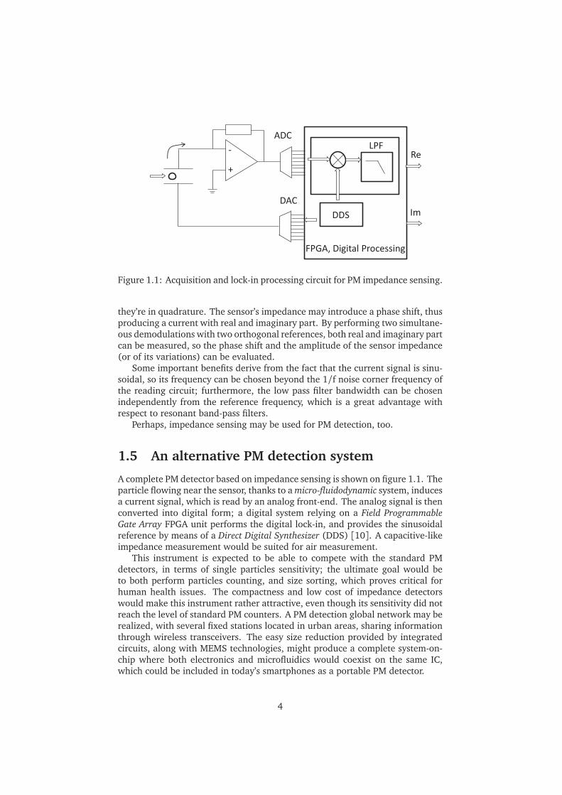
+
-
ADC
DAC
FPGA, Digital Processing
LPF Re
Im DDS
Figure 1.1: Acquisition and lock-in processing circuit for PM impedance sensing.
they’re in quadrature. The sensor’s impedance may introduce a phase shift, thusproducing a current with real and imaginary part. By performing two simultane-ous demodulations with two orthogonal references, both real and imaginary partcan be measured, so the phase shift and the amplitude of the sensor impedance(or of its variations) can be evaluated.
Some important benefits derive from the fact that the current signal is sinu-soidal, so its frequency can be chosen beyond the 1/f noise corner frequency ofthe reading circuit; furthermore, the low pass filter bandwidth can be chosenindependently from the reference frequency, which is a great advantage withrespect to resonant band-pass filters.
Perhaps, impedance sensing may be used for PM detection, too.
1.5 An alternative PM detection system
A complete PM detector based on impedance sensing is shown on figure 1.1. Theparticle flowing near the sensor, thanks to a micro-fluidodynamic system, inducesa current signal, which is read by an analog front-end. The analog signal is thenconverted into digital form; a digital system relying on a Field Programmable
Gate Array FPGA unit performs the digital lock-in, and provides the sinusoidalreference by means of a Direct Digital Synthesizer (DDS) [10]. A capacitive-likeimpedance measurement would be suited for air measurement.
This instrument is expected to be able to compete with the standard PMdetectors, in terms of single particles sensitivity; the ultimate goal would beto both perform particles counting, and size sorting, which proves critical forhuman health issues. The compactness and low cost of impedance detectorswould make this instrument rather attractive, even though its sensitivity did notreach the level of standard PM counters. A PM detection global network may berealized, with several fixed stations located in urban areas, sharing informationthrough wireless transceivers. The easy size reduction provided by integratedcircuits, along with MEMS technologies, might produce a complete system-on-chip where both electronics and microfluidics would coexist on the same IC,which could be included in today’s smartphones as a portable PM detector.
4

Chapter 2
Sensor design
2.1 General considerations
The way particulate matter interacts with the sensor is expected to be stronglydependent on the geometry of both the PM particle and the sensing electrodes,beside their material. Two geometrical approaches can be followed: the particlesmight flow between the plates of a parallel-plate capacitor; the particles mightflow, or might be deposited, above a coplanar electrodes pair, in contact to orvery close to the sensor surface.
Another free parameter is the fluid that conveys the particles: PM could re-main in the air, or it could be separated from it and added to a liquid medium.The former strategy would result in a more compact, practical, and easy-to-use device: a future development of a fully integrated microfluidic and elec-tronic system, which could be one of the several applications of nowadays smart-phones, would rather use this option, without any liquid and bulky pumpingsystems involved. On the other hand, the latter strategy would simplify the flu-idodynamics project, helping the particles to flow into the channel, thanks tothe buoyancy force. In that case either a capacitive or a resistive measurementcould be possible.
Anyway, this kind of impedance sensing, e.g. for cell counting, is widelyperformed in liquid, while air microfluidics is not so common; a device beingable to directly work in the air would be a greater accomplishment, besides thecompactness and easier integrability discussed above. For these main reasons,all the efforts have been devoted to operate with air, thus sensing a capacitivevariation.
The parallel-plate sensor has a main restriction: since one of the final goalsis to classify PM particles according to their diameter, the gap between the twoplates must be large enough to let even the bigger1 mote pass through. A cer-tain margin has to be taken into account, since PM is not actually composedby spheric objects, so a 30µm gap may be enough to prevent the channel fromclogging. Now, if the same sensor were used for every different diameters, thesmaller2 particles would probably determine a negligible perturbation of thesensing volume, being two orders of magnitude below the gap between the elec-
110µm diameter2300 nm
5

h x
Figure 2.1: Estimation of the capacitance variation of a parallel-plate sensor; anequivalent circumscribed cube has been used to obtain an analytical expressionfor the capacitive signal.
trodes. Anyway, a quantitative analysis is necessary to come to such a conclu-sion. Nevertheless, this alternative provides a constant electric field, meaning acurrent signal independent of the particle position.
Let’s now consider the coplanar case. The electric field is now less pre-dictable, though a qualitative insight can be grasped. The field lines wouldeventually arrange in a circular fashion, being likely denser at the inner edges ofthe electrodes. The field intensity now depends on the position of the particle,so a source of uncertainty is added. The most sensitive area might just be theinner edges of the electrodes, so it could be advisable to locate the particles asclose as possible to the gap; a proper focusing air flow would drive the particleto the desired position. Again, a quantitative analysis must be carried out.
2.2 Parallel-plate sensor
An analytical expression for the capacitive variation, although approximated,may be obtained by simple volume considerations, at least for the parallel-plate geometry. In this case, the expression of the capacitance is well-known:C = Aεrε0/d, where A is the area of the plates, d is the gap between them, εrε0is the absolute permittivity of the dielectric medium. The PM particle is replacedby a sphere with diameter equal to the aerodynamic equivalent diameter of theparticle (see figure 2.1).
At first, let’s consider the cube circumscribed to the sphere, having two facesparallel to the capacitor’s plates, and the same dielectric constant as the sphere.This cube is contained into a parallelepipedon, where the capacitive variationtakes place; the outer volume is a constant capacitance in parallel with it.
The parallelepipedon can be seen as the series of two parallel-plates capaci-
6

tors: the cube itself, and the air gap. Its capacitance, Cp, is equal to:
Cp =CcubeCair
Ccube + Cair
=x2εrε0
hεr + x(1− εr)
being
Ccube =x2εrε0
x
Cair =x2ε0
h− x
leading to this variation:
∆C =x2εrε0
hεr + x(1− εr)−
x2ε0
h=
x3ε0(εr − 1)
h2εr + hx(1− εr)
For small x values, i.e. for particles much less than the channel size, we see that:
∆C −→x3ε0(εr − 1)
h2εr
This formula can be rearranged in a way easier to be remembered, which alsohighlights some important features:
∆C −→ε0
hx2 x3
hx2
εr − 1
εr
= Cp
Vcube
Vp
∆εr
εr
(2.1)
Now we can see that if a volume equal to Vcube changes its permittivity, it pro-duces a capacitive variation which is a fraction of the total capacitance, accord-ing to the relative volume Vcube/Vp and to the relative permittivity variation; thislast term is always less than 1, to which it tends if εr →∞. This is reasonable:by increasing εr until the particle’s capacitance becomes much greater than Cair ,this last term becomes the significant one in the series of the two, and any furtherincrease in Ccube is meaningless.
If we now consider the spherical particle, two analogue expressions can beconstructed for the general and the approximated cases, respectively; the cube’svolume and side are simply replaced by the sphere’s volume and radius:
∆C ≃ 4/3πR3 ε0(εr − 1)
h2εr + hR(1− εr)(2.2)
∆C −→ 4/3πR3 ε0(εr − 1)
h2εr
(2.3)
To have an idea of how intense the capacitive signal could be, let’s considerplastic spheres, having εr = 2, which is a reasonable value for a consistent frac-tion of PM [2], as a function of the diameter. The gap between the plates hasbeen chosen equal to 30µm, since it must allow at least PM10 to flow. Such amargin has been taken because real particles are not spherical at all, so one mustbe careful to avoid the clogging of the channel.
7

Figure 2.2a is a log-log plot of the capacitive variation, according to equation(2.2). The slope is 60 dB per decade, clearly proving that the signal is propor-tional to the particle’s volume, as in equation (2.3).
Regarding PM10, we therefore expect ∆C ≈ 3 aF, an easily achievable sensi-tivity for most of the electronic instrumentations [11]. When dealing with PM2.5,things drastically change: for a 1µm particle the signal has decreased to 3 zF,3
a very difficult value to measure even for an integrated system [12].This geometry doesn’t seem to be suited to detect PM2.5. One could object
that this is a consquence of the channel sizing, in order to measure all the differ-ent diameters together. If the particles were previously sorted, the finer fractionmight be sensed by a customized sensor, e.g., with a 3µm gap (see figure 2.2b).In that case, the variation would rise back to more than 3 aF, making it a verypromising solution. However, there are some major drawbacks, mainly due totechnological issues. This geometry would require a non standard fabricationprocess, which so far is not available. Secondly, the fractioning stage would risethe complexity of the microfluidic design.
In conclusion, this geometry has the potentiality to detect the particles withinthe desired diameter range, but, for the reasons listed above, the coplanar ge-ometry will be now investigated.
2.3 Coplanar electrodes sensor
2.3.1 Coarse estimation
A couple of coplanar plane electrodes is shown in figure 2.3: they act as a ca-pacitor. The electric field lines have been traced in a qualitative way. Theseelectrodes can be easily fabricated over a glass substrate, by means of a litho-graphic process. Then, a microfluidic channel is placed on this surface; a moldedlid made of Polydimethylsiloxane (PDMS) is generally used for the purpose. Anair flow containing PM particles flows into this channel. Since the electric fieldis supposed to be more intense at the surface, near the gap between the elec-trodes, the particles should flow as close as possible to that position; a secondaryair flow, orthogonal to the surface, may force the particles to this condition.
It is now clear the main advantage of this geometry: a single couple of elec-trodes could be used to sense particles of different size, if the air flow wereconveyed as explained above. In case different parameter choices were moresuited for different particle diameters, an array of optimized electrodes could berealized as well.
The expected capacitive variation, is, however, much more complex to de-termine, due to the non homogeneous electric field distribution. The conformalmapping method allows to derive an expression for the capacitance per unitlength of two coplanar electrodes, as shown in Chen et al. [13]:
C = 2ε0
εr1 + εr2
2πln
1+2L
G
+
√
√
1+2L
G
2− 1
W (2.4)
3Now the diameter is reduced by a factor of ten; the signal scales with the volume, a ten to thecube factor.
8

100m 1 10
1E-5
1E-4
1E-3
0,01
0,1
1
10
h=30µm
∆C
(aF
)
Diameter (µm)
(a) h=30µm.
0,01 0,1 1
1E-5
1E-4
1E-3
0,01
0,1
1
10
h=3µm
∆C
(aF
)
Diameter (µm)
(b) h=3µm.
Figure 2.2: Log plot of the capacitance variation, using the general formula; theslope is practically 60 dB per decade, i.e. the variation is proportional to theparticle’s volume.
9

G
D
L
W
h
Figure 2.3: A couple of coplanar electrodes with their geometric parameters.
where G is the gap between the electrodes, L is their longitudinal width, Wis their transversal width, εr1 and εr2 are the relative permeabilities of the half-spaces separated by the electrodes; the glass substrate has εr = 4.6, while theupper half-space is filled with air.
For a pair of electrodes having G = 10µm and L = 20um, this is equal to36 aFµm−1. If the electrodes were 100µm wide, the total capacitance wouldbe 3.6 fF. By analogy with the parallel-plate geometry, the capacitive varia-tion should be proportional to the particle’s volume over the total capacitancevolume, which resembles a cylinder of radius L + G/2 = 25µm and heightW = 100µm. Since the medium is half air and half glass, it is convenient toconsider only the upper half of the cylinder, weighting it by 1/(1+ εr) ≈ 0.18(if it were all air, it would be correctly equal to 1/2). The signal due to a plasticsphere (εr ≈ 2) can be estimated as already done for the parallel-plate case,applying equation (2.1):
∆C ≈ Ctotal
Vsphere
Vtotal
∆εr
εr
= 3.6 fF1
1+ εr
4/3πR3
π(L + G/2)2W/2
∆εr
εr
= 1.7 aF
The result is encouraging, but this is of course a quite naive way to proceed.The conformal mapping method cannot be used to compute the capacitance inpresence of a particle, therefore another approach is necessary to estimate withmore accuracy the corresponding capacitive variation. A Finite Elements Method(FEM) simulation will be carried out in COMSOL Multiphysics; the value fromthe conformal mapping approach will serve as a cross check for the capacitanceof the mere sensor.
2.3.2 Finite elements simulations
A series of 3D time-harmonic simulations with COMSOL Multiphysics have beenperformed, in order to estimate the capacitive signal for the coplanar geometry.Before exploring in depth every possible configuration for the electrodes, the sig-nal order of magnitude is derived for a generic coplanar electrodes arrangement;
10

Figure 2.4: Simulation domain; two symmetry planes have been exploited.
the following example will show the approach adopted in all the other simula-tions. The dependence from the parameters involved will be studied later.
With reference to figure 2.3, a 10µm diameter (D) sphere, with its centerat 10µm above the surface, has been placed between two coplanar electrodes.It seems reasonable to keep the sphere at such a distance from the pair, sincea smaller value may cause the particle to hit them; moreover, the channel ex-tends for 50µm in height, that limits the vertical position of the sphere. Theelectrodes are separated by a 10µm gap (G), while their longitudinal width (L)is 20µm; such values match the diameter, for the electric field is expected tobe properly perturbed in this configuration. The y-direction width (W) is muchgrater than L, since it must accommodate the microfluidic channel: a value of1 mm is reasonable.
The physical domain implemented by the simulator is shown in figure 2.4.Actually, the overall volume of figure 2.3 has been divided in four parts, in or-der to exploit two symmetry planes; only a quarter volume is considered in thesimulations, thus saving in computation. Therefore, only one half of electrodeis visible, as well as a quarter of sphere. The electrodes have been truncated to100µm (only a 50µm half electrode is visible), which is likely wide enough toinclude all the perturbation due to a 10µm particle. The remaining part of themis a parallel constant capacitance which produces no signal. The technologicalprocess employed limits the thickness of the electrodes to about 200 nm, whichhas been neglected in the simulation domain.
Boundary conditions have to be chosen properly. Let’s consider the wholevolume, as in fig. 2.3. One electrode is stimulated by a sinusoidal voltagesource, while the other one will be connected to the virtual ground of the tran-simpedance amplifier. The two electrodes have both a common mode and adifferential mode voltage applied. The common mode voltage induces no cur-
11

Sub-domain εr
GLASS 4.6PDMS 2.75AIR 1SPHERE 2
Table 2.1: Subdomains permittivities.
rent into the sensor, therefore only the differential mode matters in order tocalculate the capacitance of the sensor. We could reach the same result by ap-plying a pure differential voltage between the electrodes: half of the voltage atone electrode, and the same half but with opposite sign at the other one. Nowthe electrostatic potential has an odd symmetry with respect to the y-z planethat crosses the origin4, which must be at zero Volts. By forcing this plane toa ground boundary condition, we can simply forget the negative-x half-space,and compute the overall capacitance by halving the capacitance seen by the re-maining electrode towards ground; this capacitance can be easily obtained bythe admittance matrix returned by the program.
Now, let’s consider the x-z plane: the electrostatic potential has an even sym-metry with respect to this plane, i.e. no displacement current flows through it.So, nothing change if we split the remaining electrode by forcing an electricalisolation boundary condition at this plane. Again, we can forget the negative-y half-space, and compute the overall capacitance by doubling the capacitanceseen by the remaining electrode towards ground.
To summarize, if both the conditions are applied, the total capacitance isequal to the one corresponding to that quarter of space. All the other externalboundaries have been set to electrical isolation, and the internal ones to thecontinuity of two dielectric regions, except for the half-electrode area, whichhas been set to a port with forced voltage.
All the geometric sub-volumes are dielectrics; their permittivities have beenchosen as in table 2.1. The simulation domain is the same for both the casewith the sphere and without it; one can shift from the former to the latter bysimply changing the permittivity of the quarter-of-sphere subdomain, from 1 (nosphere) to 2 (sphere with εr = 2). The main reason for this operating choiceis that it keeps the same FEM mesh; if not, the capacitance variation would bemainly due to the mesh change, that would have absolutely no sense.
The simulator returned 3.871 951 fF for the initial capacitance (very close tothe conformal mapping value), and a variation of 2.397 aF. This last value isof the same order of magnitude of the one estimated in section 2.3.1, but un-doubtedly more reliable. This result suggests that coplanar sensors have signalperformances similar to parallel-plate sensors; however, this has been verifiedonly for the 10µm particle, with a quite arbitrary choice of the parameters in-volved. Hence, many other different situations must be simulated, in order tounderstand how these parameters affect the signal, and how to use this infor-mation for the design of the optimum sensor.
4Same reference system of fig. 2.4.
12

Name Description
D Particle’s diameterG Gap between the electrodesL Electrode’s lengthW Electrode’s widthh Distance of the particle’s center
from the surfaceεr Particle’s dielectric permittivity
Table 2.2: Coplanar electrodes parameters.
Fixed parameters G C0 C ∆C
Name Value (µm) (fF) (fF) (aF)
D (µm) 10 20 3.164569 3.165 938 1.369L (µm) 20 15 3.446 417 3.448230 1.813W (µm) 100 10 3.980 185 3.982602 2.417h (µm) 10 6 4.513067 4.515 964 2.897εr 2 4 5.142 898 5.145987 3.089
2 6.193249 6.196 461 3.2121 7.216955 7.220 184 3.229
Table 2.3: Capacitive variation as a function of the gap G.
2.3.3 Parameters dependences
The main parameters involved have been introduced in the previous subsection,and they are listed in table 2.2. The signal’s dependence from each of them willbe studied, keeping the other ones constant. The computing approach is thesame as in the first case-study.
Let’s start with the gap G. The results of the simulations are summed up intable 2.3. On the left side the constant parameters have been listed; on the rightside, next to each gap value, the sensor initial capacitance (C0), the capacitanceperturbed by the sphere (C), and the corresponding variation (∆C) are shown.
As we could expect, the total capacitance increases by reducing the gap, sim-ilarly to a parallel-plate capacitor. In fact, if the gap is reduced, a grater electricfield is necessary to maintain the same voltage5 between the electrodes, there-fore more charge has to be placed on them, thus increasing the capacitance. Thecapacitive variation also increases by reducing the gap, which might be the veryfirst guideline for the sensor project.
The next parameter to be studied is the relative permittivity εr . Table 2.4shows, as predictable, a capacitance gradually increasing with the permittivity;this increase is not, however, indefinite; following the analysis of section 2.2 asthe particle’s capacitance becomes dominant with respect to the air capacitance,the series is approximated only by the smaller one, without being affected by fur-ther changes of the permittivity. This has already been highlighted in equation(2.1), and figure 2.6 clearly depicts this trend.
5∆VAB = −∫ A
B~E ~dl
13

0 2 4 6 8 10 12 14 16 18 20 22
0.0
0.5
1.0
1.5
2.0
2.5
3.0
3.5
∆C
(aF
)
G (µm)
Figure 2.5: Capacitive variation as a function of the gap G.
Fixed parameters εr C ∆C εr C ∆C
Name Value (fF) (aF) (fF) (aF)
D (µm) 10 1 3.761525 0.000 20 3.769 826 8.301L (µm) 20 2 3.763 920 2.395 30 3.770238 8.713W (µm) 100 3 3.765359 3.834 40 3.770454 8.929h (µm) 10 4 3.766 320 4.795 50 3.770587 9.062G (µm) 2 5 3.767008 5.483 60 3.770 677 9.152
6 3.767523 5.998 70 3.770 742 9.2177 3.767925 6.400 80 3.770 791 9.2668 3.768246 6.721 90 3.770 830 9.3059 3.768509 6.984 100 3.770 861 9.336
10 3.768 728 7.203 1000 3.771116 9.591
Table 2.4: Capacitive variation as a function of the relative permittivity εr .
14

0 20 40 60 80 100 120
0
2
4
6
8
10
∆C
(aF
)
εr
Figure 2.6: Capacitive variation as a function of the relative permittivity εr .
The permittivity is strictly linked to the material whom the particle is madeof, therefore the consequences on PM detection are twofold. For a given diame-ter, different permittivities lead to different signal levels; the resulting detectorwould be able to distinguish and sort the particles according to their material,which is quite an accomplishment. On the other hand, this would imply to havealready sorted PM in diameter classes, but this is just the detector’s job. The pri-mary goals are to detect PM and to measure its diameter through an impedancemeasurement, so the variability due to the permittivity looks more like a draw-back, rather than a valuable feature. Let’s consider figure 2.6: a 10µm particlewith εr = 2 would lead to a 2.4 aF signal; a similar particle with εr = 3 gives3.8 aF, so the corresponding variation is 1.4 aF. The same variation could beproduced by a change in the particle’s diameter, therefore it could be misinter-preted; a valid criterion must be developed in order to correctly interpret thecapacitive information.
Anyway, for large permittivity values, the capacitive signal saturates at about10 aF. For εr > 15 the variation is fairly negligible when transduced into diam-eter uncertainty, considering that the geometrical dependence is much heavier(to the particle’s volume).
At this point, the diameter dependence must be faced. The simulations re-sults are listed in table 2.5. The FEM domain is now a bit different. A seriesof concentric spheres, one per diameter value, has been used instead of a singlesphere. When considering a certain diameter value, one must simply set the cor-rect value for the spherical shells. This is the reason for the initial capacitanceC0 remains constant, being the mesh unchanged for each simulation.
The dependence on the permittivity has also been taken into account: thediameter varies while εr = 2 or εr = 15. As expected, the signal is greater
15
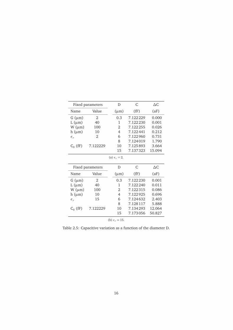
Fixed parameters D C ∆C
Name Value (µm) (fF) (aF)
G (µm) 2 0.3 7.122 229 0.000L (µm) 40 1 7.122 230 0.001W (µm) 100 2 7.122 255 0.026h (µm) 10 4 7.122 441 0.212εr 2 6 7.122 960 0.731
8 7.124 019 1.790C0 (fF) 7.122229 10 7.125893 3.664
15 7.137323 15.094
(a) εr = 2.
Fixed parameters D C ∆C
Name Value (µm) (fF) (aF)
G (µm) 2 0.3 7.122 230 0.001L (µm) 40 1 7.122 240 0.011W (µm) 100 2 7.122 315 0.086h (µm) 10 4 7.122 925 0.696εr 15 6 7.124 632 2.403
8 7.128 117 5.888C0 (fF) 7.122229 10 7.134293 12.064
15 7.173056 50.827
(b) εr = 15.
Table 2.5: Capacitive variation as a function of the diameter D.
16

0 1 2 3 4 5 6 7 8 9 10 11 12
0
2
4
6
8
10
12
14
16
18
20
∆C
(aF
)
D (µm)
εr=15
εr=2
Figure 2.7: Capacitive variation as a function of the diameter D.
for εr = 15 when the diameter is the same. The most important result fromthis analysis is, however, the strong dependence of the signal by the particle’svolume. From tables 2.5a and 2.5b one can verify that by halving the diameter,the capacitive variation scales by a factor of 8, and so on. This dependencecannot be taken as a stern general rule, the electric field not being constant. Itworked pretty well for these particular situations, and we might explain it byobserving that the diameter was changed ’in the proper way’. Let’s consider the5µm sphere; the electric field is stronger below it, and weaker above it (it willbe verified in the next lines). By doubling the diameter while keeping the samedistance h, the new volume extends itself both above and below, thus keepingthe same average electric field, more or less.
In the worst scenario, i.e. for εr = 2, detecting a 8µm might be very difficult,looking at the values predicted by the FEM. Greater values are expected if theparticle gets closer to the surface, so the next parameter under investigation isthe distance h, that is the distance of the sphere’s center from the surface. Table2.6 and figure 2.8 show the results, that indicate an increase in capacitive signalas the sphere gets closer to the surface, according to the picture of a more intenseelectric field in the gap region. It would be desirable to keep the particles at theminimum possible distance, to maximize the signal.
If we concentrate on the horizontal flow model, we must keep a minimumdistance to let the particles flow; moreover, if all the PM is intended to be mea-sured in a single air flow, the smaller particles have to remain into the same layerof air that also carries the bigger particles; these are the ones which determinethe minimum value for the distance h, which may be inadequate for measuringthe smaller ones.
A totally different measurement approach may overcome this issue: instead
17

Fixed parameters h C0 C ∆C
Name Value (µm) (fF) (fF) (aF)
D (µm) 10 5 3.930502 3.937 515 7.013G (µm) 10 6 3.870561 3.876 004 5.443L (µm) 20 7 3.920 827 3.925245 4.418W (µm) 100 8 3.942 593 3.946190 3.597εr 2 9 3.916 833 3.919767 2.934
10 3.887 811 3.890231 2.42011 3.887 910 3.889906 1.99612 3.727 595 3.729237 1.64213 3.855 227 3.856612 1.38514 3.878 345 3.879522 1.17715 3.861 428 3.862425 0.99720 3.764 488 3.764955 0.46725 3.798 903 3.799141 0.23830 3.806 880 3.807010 0.13035 3.797 085 3.797158 0.073
Table 2.6: Capacitive variation as a function of the distance h.
0 5 10 15 20 25 30 35
0
1
2
3
4
5
6
7
8
∆C
(aF
)
h (µm)
Figure 2.8: Capacitive variation as a function of the distance h.
18

Fixed parameters L C0 C ∆C
Name Value (µm) (fF) (fF) (aF)
D (µm) 10 2 1.566503 1.567 091 0.588G (µm) 10 5 2.137153 2.138 298 1.145W (µm) 100 10 3.026 394 3.028210 1.816h (µm) 10 15 3.478472 3.480 655 2.183εr 2 20 3.761525 3.763 920 2.395
30 4.303 638 4.306269 2.63140 4.711 345 4.714041 2.69650 4.907 003 4.909727 2.724
100 5.924799 5.927 615 2.816
Table 2.7: Capacitive variation as a function of the length L.
of making PM travel as close as possible to the surface in a laminar flow, theparticles may drop on the electrodes from above, provided that they alwaysreach a sensitive area with high probability.
The last parameter to analyze is the length L. It is difficult to find an analogueparameter for an equivalent parallel-plate capacitor, that may help to predict thisdependence. In some way it is related to the plates area; if L increases, then thetotal capacitance is expected to increase, too, that has been well highlighted byequation 2.4. However, increasing L also produces a greater capacitance vari-ation, that means a more intense electric field. Figure 2.10 shows the electricpotential isosurfaces in the sensor region: it varies from 1 V (red) to 0 V (blue).The sensor’s electric field (2.10a), being orthogonal to the isosurfaces, comesout of the plate in a quite circular fashion, except for the gap region, whereit goes directly towards the other electrode. The electric field arrangement re-sembles the one generated by a punctiform charge dipole, but in this case thetwo ’charges’ are the coplanar plates. A sphere with εr = 10 (2.10b) perturbsthe electric field: the isosurfaces bend, and they are now less dense into thesphere’s volume, where the electric field becomes less intense. It is desirablethat the initial electric field perturbed by the sphere is as intense as possible, i.e.the isosurfaces have to be dense. Figures 2.10c and 2.10d show a close-up com-parison between sensors having L=20µm and L=50µm. In the latter case theremore isosurfaces are going to be intercepted by the sphere, so their gradient isgreater, meaning a more intense electric field, thus producing a more intensecapacitive variation.
In conclusion, the length L should be maximized to get the highest sig-nal. This improvement is not, however, infinite, as depicted in figure 2.9. Atsome point (30µm for this particular situation) the capacitance rises much moreslowly, being any further increase in L totally useless. One must also rememberthat L makes also the total capacitance grow up, which may represent a draw-back (it adds more parasitics to the processing stage, for example).
19

0 20 40 60 80 100
0.0
0.5
1.0
1.5
2.0
2.5
3.0
∆C
(aF
)
L (µm)
Figure 2.9: Capacitive variation as a function of the length L.
2.4 Oblique electrodes
The parametric simulations have shown a quite predictable result: in order tomaximize the capacitive variation, one must increase the electric field perturbedby the particles; this has been accomplished, for example, by reducing the gapbetween the electrodes. To increase the electric field, for a given voltage betweenthe electrodes, means ’to compress’ the isosurfaces of the electric potential, atleast around the gap region, which is the most sensitive one. If the electrodescould lean in an oblique position, but still allowing the particles to flow betweenthem, there might be some improvement. This idea is halfway between thecoplanar and the parallel-plates geometries, and is shown on figure 2.11. Sucha pair of electrodes, at about 45 with respect to the surface, can be actuallyrealized by the technological process employed**inserire riferimento tecnolo-gia**, but the cost is higher; one must analyze this geometry, and see if theimprovements justify the greater cost.
Table 2.8 summarizes the results. The parameters have exactly the samemeaning for both geometries, and they have already been defined previously.The one not shown are the distance from the surface h (10µm), the electrodes’length L (30µm), and width (100µm). We see that the corresponding capacitivevariation is greater for the oblique geometry of a factor of two, more or less.Although this arrangement leads to an improvement, it is not worth the risk:the 10µm particle produces a signal which is already detectable by the currentinstrumentations. Doubling the signal is quite an accomplishment, but it doesnot justify the employment of a more complex technological process, nor theincreased complexity of the fluidodynamic project, at least at such a preliminarydesign stage.
20

(a) εr=1. (b) εr=10.
(c) L=20µm. (d) L=50µm.
Figure 2.10: Electric potential isosurfaces in the sensor region.
D G εr C0 C ∆C
(µm) (µm) (fF) (fF) (aF)
10 10 2 4.413687 4.416 305 2.61810 10 15 4.413687 4.422 346 8.6592 2 2 6.717573 6.717 597 0.0242 2 15 6.717573 6.717 653 0.080
(a) Coplanar electrodes.
D G εr C0 C ∆C
(µm) (µm) (fF) (fF) (aF)
10 10 2 7.416966 7.421 686 4.72010 10 15 7.416966 7.432 775 15.8092 2 2 10.888022 10.888 085 0.0632 2 15 10.888022 10.888 229 0.207
(b) Oblique electrodes.
Table 2.8: Comparison between coplanar and oblique electrodes.
21

G
h L
W
D
Figure 2.11: A couple of oblique electrodes and their geometric parameters.
2.5 Pulse shape
The signal produced by the sensor depends on the way it is operated. If theparticulate drops on the sensor in a sensitive area, the capacitance varies as astep function, with a slope related to the falling speed of the particles. Con-versely, if they flow above the electrodes, the capacitance varies only for a brieftime interval, which is related to the particle’s speed. It could be interestingto study this pulse shape depending on the particle’s diameter: if different di-ameters produce different shapes, this property would give a criterion to sortthem in size classes even if there is a variability of permittivity. The pulse shapesproduced by a set of spherical beads, with the same permittivity and differentdiameters, would be measured and stored. Instead of a standard low pass filter,the lock in amplifier could perform a synchronous filtering, testing all the storedpulse shapes in parallel; the one that matches the particle’s unknown diame-ter produces the highest value, and is the optimum filter. Once the diameteris identified, the pulse height would depend only on the particle’s permittivity.This approach needs more filtering stages in parallel to be done in digital do-main, so the required FPGA performances would be more severe. Furthermore,we are assuming the pulse shape not to be dependent on the permittivity.
The pulse shape has been estimated by moving the sphere along the channel,and then measuring the static capacitive variation for each position. This time,only one symmetry plane has been exploited, therefore the usual geometric do-main had to be changed accordingly. This has been done for two spheres having
22

Fixed parameters x C0 C ∆C ∆CNORM
Name Value (µm) (fF) (fF) (aF) (m−1)
D (µm) 2.5 0 2.516814 2.516 882 0.136 80188.7G (µm) 4 2 2.493333 2.493 401 0.136 80 188.7W (µm) 100 4 2.498 860 2.498925 0.130 76 651.0h (µm) 10 6 2.499426 2.499 484 0.116 68396.2εr 15 8 2.494570 2.494 621 0.102 60141.5L (µm) 20 10 2.489 407 2.489451 0.088 51 886.8Area (aF µm) 1.696 12 2.468798 2.468 835 0.074 43632.1
14 2.491 210 2.491243 0.066 38915.1
(a) D=2.5µm
Fixed parameters x C0 C ∆C ∆CNORM
Name Value (µm) (fF) (fF) (aF) (m−1)
D (µm) 10 0 2.516814 2.521 872 10.116 81451.9G (µm) 4 2 2.493333 2.498 381 10.096 80188.7W (µm) 100 4 2.498 860 2.503595 9.470 76 250.4h (µm) 10 6 2.499426 2.503 671 8.490 68359.7εr 15 8 2.494 570 2.498257 7.374 59 373.9L (µm) 20 10 2.489 407 2.492596 6.378 51 354.3Area (aF µm) 124 12 2.468798 2.471 531 5.466 44011.1
14 2.491210 2.493 564 4.708 37907.8
(b) D=10µm
Table 2.9: Derivation of the pulse shape from static capacitive variations, for asphere having εr = 15.
εr = 15 and diameters of 2.5µm and 10µm (see figure 2.12 and table 2.9).The pulse shapes have been normalized to their respective areas, so that they
have unitary area, for a fair shape comparison. The results show that there is ac-tually no difference between them, thus ruling out the optimum filter approachfor distinguishing diameter variations from permittivity variations. Neverthe-less, the particles could be separated according to their diameter before beingsensed, by exploiting microfluidodynamic properties; this has already been ac-complished by [14], who separated particulate matter by size directly in the air.
This analysis provides with some information on the pulse time duration,which is related to the signal’s bandwidth, and dictates some specifications forthe system. Looking at the figure, the pulse is produced on a spatial range ofthe order of 10µm around the gap. This means that if the particles travels at1 mm/s, the pulse lasts 10 ms, so its bandwidth is 100 Hz; the system’s band-width after lock-in operation determines the system’s noise and the minimumdetectable amplitude, so it can be set to the same value, or a decade beyond.One may set the minimum particle’s speed for fluidodynamic issues, and thenobtain the minimum lock-in bandwidth; or, which is indeed the case, one canset the maximum lock-in bandwidth for a given sensitivity, which automaticallyfixes the maximum particle’s speed. In order to reach such a sensitivity (1 aF),
23

0,000
0,200
0 1 2 3 4 5 6 7 8 9 10
0
10000
20000
30000
40000
50000
60000
70000
80000
90000
0 2 4 6 8 10 12 14
D=2.5um
D=10um
Figure 2.12: Comparison between the pulse shapes produced by two sphereswith different diameters.
the lock-in amplifier cannot afford a bandwidth greater than 1 kHz, [11], so theparticle’s speed has to be limited to 10 mm/s.
This compromise is absent if we adopt the vertical fall approach, instead ofthe horizontal flow one: in that case, the particles drop at their regime speed,and the system can detect the low frequency changes of the capacitance’s steadystate value.
2.6 Theoretical sensitivity
In the previous sections some geometric configurations have been analyzed, aim-ing to find out the most suitable for a capacitive measurement in the air of par-ticulate matter. The simulations have shown that the coplanar configuration isthe best compromise between sensitivity and fabrication simplicity. It has beenshown that this geometry should be able to detect a particle of 10µm diameter,even for the lowest permittivity value, and with the particle flowing at a certaindistance from them, i.e. PM10 should be well detectable. However, this detectoris intended to measure also finer particles, so the sensitivity to the 1µm diame-ter particle is now investigated. To do so, the particle has been placed in touchwith the surface, being the most sensitive area; the gap has been minimized tothe minimum available value of the technological process employed, i.e. 2µm.The simulator returns 0.96 aF when εr = 15, and 0.28 aF when εr = 2. Only forhigh permittivity values we get close to the reference value of 1 aF.
May these signals not be enough for the detection, the measurement couldbe performed in water, instead. Water has been neglected so far, because it im-plies a more complex management system: somehow PM must be transferredfrom air into water, that may be possible, but it rises the complexity of the flu-idodynamic project. Then, water impedance measurement have widely beenperformed because of the higher obtainable signal, so that would not be a sat-isfying result. If needed, a water measurement could be resistive or capacitive,depending on the water conductivity; typical values are 1 S/m for a saline com-pound behaving like a resistance, or zero for distilled water, which behaves likea capacitance. Water relative permittivity is about 80. The simulation resultsare listed in table 2.10.
Water measurements are clearly superior in terms of signal level: a 1µm
24

εr ∆Cair ∆Cwater ∆Rwater ∆Gwater
(aF) (aF) (Ω) (nS)
2 0.28 -48 3 8315 0.96 -37 3 83
Table 2.10: Size sensitivity comparison between air and water measurements.
particle could be well detectable either with a capacitive or a resistive measure-ment; the capacitive one gives variations (negative, since the permittivity in thesphere region lowers) of the order of tens of atto Farad; the resistive variationsare even of the order of one Ohm. Although these promising performances, asalready said, the water measure is not challenging, and it will be put aside; incase the air measurement won’t give the expected results, water measurementwill be the second-best solution.
2.7 Sensor layout
The sensors have been fabricated according to the coplanar geometry, followingthe horizontal flow approach. They are basically plane metal lines deposited ona glass substrate, consisting of an 8 inch glass wafer. The electrodes are madeof gold, but there is also a thin (20 nm) adhesion layer made of titanium; theoverall electrode’s thickness is 200 nm. The wafer layout is shown on figure2.14. The area has been divided into four main slides, named "A" "B" "C" and"D" starting from top, and into four little slides at the sides, all named E, sincethey are all equal.
The main slides differ for some parameter choices, but they all share the samestructure (see fig 2.13). On the right side there is an array (named "d") of fivecouples of electrodes, numerated from 1 to 5 starting from left. These are thesensing electrodes that the particle flowing from left to right would encounter,thus producing a series of five pulses for a single travel, one per sensor (theyhave been sufficiently separated to avoid the superposition of different pulses).These sensors have one parameter varying, so that the traveling particle wouldproduce different pulses; the aim is to validate the parameter dependences in-ferred from the previous simulations. Electrodes "Ad" have L=30µm, but gapequal to 2, 4, 6, 10 and 20µm from left to right, respectively. The lithographicresolution is about 2µm, which dictates the minimum gap value, although the4µm one is expected to be more reliable in terms of unwanted short-circuits.Moreover, only on slide A, the electrodes with gap 4 and 10µm are not couples,but triples with two gaps per each, in order to perform a differential measure-ment. The two outer electrodes will be driven by voltage sinusoids in phaseopposition, and the inner one will sink the two currents produced, thus per-forming an intrinsic difference operation: if there is no particle, and everythingis perfectly balanced, no net current is read by the processing stage; if the parti-cle is flowing, it unbalances the sensor, and a bipolar current signal is produced.Electrodes "Bd" have all the same gap, equal to 4µm, which maximizes the sig-nal, but they have different length L; its values are 10, 20, 30, 60 and 100µm.Electrodes ’Cd’ are basically the same as "Ad", but there aren’t any triples. Elec-
25

Figure 2.13: Close-up of a single rectangular slide; the the two groups "s" and"d" are indicated, as well as the single electrode’s progressive numbers.
trodes ’Dd’ are similar to ’Cd’, but L has been set to 100µm, in case the otherswould prove to be too much weak.
The width W has been chosen equal to 1.5 mm, since the air channel resultingfrom the PDMS mold is 500µm wide, and it must be correctly aligned. Of course,the greater the width, the greater the overall sensor capacitance. In this case, themost critical value expected is around 200 fF, which is negligible with respect tothe parasitics of the following discrete components circuit, that are likely of theorder of some pico Farad.
Still on the main slides, on the left side there is a group of three sensors,named "s". These are related to the fluidodynamic project. One of the optionsto drive the air flows was the creation of a lower level circular region (well),preceding the sensing area, where the particles could be properly conditionedin order to reach the sensors at the desired speed and height. The group "s"should track the particles into the well, to validate the fluidodynamic project.Anyway, for the first manufacturing process there isn’t any well, and the twogroups have been simply fabricated on the same level. These ’well’ electrodeshave been then replicated on the "E" slides; they have a 4µm gap, 100µm length,and 3 mm width.
All the electrodes have been linked by metal traces to their respective outerpads, which are located at the upper and lower edges of the slide. The padshave been associated alternating the two edges, in order to avoid capacitivecouplings between the two (or three) electrodes of the same sensor, trying tokeep the upper and lower edges as symmetrical as possible. All the sensors onthe main slides have been gathered in the middle, to leave room for the inletand outlet paths on the left and right side.
26

Figure 2.14: Whole wafer image: the capital letters indicate different slides.
27

Chapter 3
Analog front end design
3.1 Introduction
The capacitive sensor is stimulated by a sinusoidal voltage waveform, and itproduces a phase quadrature sinusoidal current; when the particle perturbs theelectrodes, causing the capacitance to vary in time, this current experiences aweak amplitude modulation,1; this is the signal that has to be detected by a lockin demodulation. The following processing stages work on voltage signals: atransimpedance amplifier is therefore necessary. It converts the capacitive cur-rent into a voltage waveform; moreover, it should desensitize the transducedsignal from the noise of the following stages. When this condition is verified,only the preamplifier limits the minimum detectable current, that must be com-pared to the noise of the transimpedance itself, which is therefore one of themost critical parameters. As already discussed, in order to read capacitive vari-ations of 1 aF, an equivalent noise bandwidth of 1 kHz will be considered.
The frequency of the sinusoidal reference also affects the signal-to-noise ra-tio. The 1/f noise corner frequency of an opamp can easily reach values suchas 10 kHz, so the reference’s frequency may be chosen between 100 kHz and10 MHz; the upper limit is set by the time delays, which become significant atthose frequencies. The modulated signal is then expected to have a narrowrelative bandwidth around a certain frequency value, which must optimize themeasurement sensitivity. The transimpedance is then required to work up to10 MHz.
The simplest and most immediate topology for a transimpedance is certainlythe OPAMP with feedback impedance, that reads the sensor’s current from thevirtual ground; this circuit is described in section 3.2. It has been adopted asa basic choice for the very first measurements. Afterwards, the employment ofan inductor to improve the sensitivity is studied in section 3.5; finally, a higherresolution preamplifier has been designed, which is described in section 3.6.
The reading circuit also include an inverting buffer that provides the samereference, but with opposite sign, in order to perform a differential measure-ment. The advantage with this approach is twofold: the noise from the genera-tor of the reference signal is reduced (ideally it should be canceled); the output
1The total capacitance of the sensor is of the order of 100 fF, while the signal is about 1 aF, sothere are five orders of magnitude between them.
28

Figure 3.1: Very simple transimpedance amplifier attached to the capacitive sen-sor.
dynamic range specifications for the transimpedance amplifier are much lesssevere.
3.2 Integrator
3.2.1 Main features
Figure 3.1 shows the classic transimpedance amplifier with feedback impedancebetween the output node and the inverting input node. In this case, a capacitorwas chosen as feedback impedance, so that the voltage gain between the out-put and the reference voltage sinusoid will not be frequency dependent, and itwill be easily adjusted in order to satisfy the output voltage range; the currenttrasduction into voltage will be fixed, too; moreover, if a resistance had beenplaced, instead, it would have added its thermal noise, while a pure capacitanceis noise free.
The feedback impedance is not actually purely capacitive: a resistor has beenplaced in parallel to C f , in order to set the bias point. As mentioned before, thisresistance adds its thermal noise, so the value must be chosen properly. A 1 GΩresistance carries 4 fAHz−1/2, which will be shown to be negligible with respectto other noise sources.
By applying a voltage sinusoidal input with amplitude A0, the output nodealso swings sinusoidally, between ±A0Cs/C f . When a capacitive variation of thesensor C f occurs, due to some PM flowing over the electrodes, a current signalis produced:
is = jω∆CA0
This current is read by the transimpedance virtual ground, and then converted
29

+
-
V+
V-
Cf
Rf
Cp
Cs
SV,s
4kTRf
SI,opamp
SV,opamp
Figure 3.2: Same circuit, but noise sources have been highlighted.
into an output voltage signal:
vout =∆C
C f
A0
Of course, there is a minimum detectable signal: noise sources limit the system’sresolution. Beside converting current into voltage, the transimpedance desensi-tizes the signal by the following stages’ noise, which should be considered negli-gible. Under this assumption, noise analysis will be carried out by referring thesignal-to-noise ratio (SNR) to the currents entering the virtual ground; both sig-nal and noise are then amplified by the same amount by the feedback capacitor,thus keeping the SNR unchanged at the output node.
Three noise sources must be considered: the opamp, the feedback resistor,and the input voltage generator. The resistance’s noise current has a spectraldensity equal to 4kT/R f , which is directly read by the virtual ground, as wellas the current input equivalent noise of the opamp. The input generator noisefollows the same transfer as the input reference signal, giving a current spectraldensity equal to SV,gen(ωCs)
2. The voltage noise of the opamp is transferred atthe output node by the noninverting gain:
SV,opamp
1+Cs + Cp
C f
2
which is equivalent to the following current at virtual ground:
SV,opampω2(C f + Cs + Cp)
2
The capacitor Cp represents both the input capacitance of the opamp and the
30

parasitic capacitance of the connections at the virtual ground node. These twonoise sources are uncorrelated, hence their squared values are summed.
The SNR of the current entering the virtual ground can be then written thisway: 2
SNR=A0ω∆C
pBWq
SV,s(ωCs)2 + 4kT/R f + SI ,opamp + SV,opampω
2(Cs + Cp + C f )2
(3.1)Having considered white noise sources, the SNR has two trends: at low frequen-cies the current generators are dominant, therefore the overall noise is almostconstant, while the SNR has a +20 dB/dec slope; at higher frequencies the otherterms, which are proportional to the frequency, become significant, preventingthe SNR from increasing any more. At one decade beyond the corner frequencythe SNR can be approximated with this expression:
SNRmax =A0∆C
pBWq
SV,sC2s+ SV,opamp(Cs + Cp + C f )
2(3.2)
Clearly, the circuit is going to work at sufficiently high frequencies, in orderto maximize the SNR. The loop gain provides information on the closed loopbandwidth and on the system’s stability:
Gloop(s) = −1+ sR f C f
1+ sR f (C f + Cp + Cs)A(s)
where A(s) is the opamp’s transfer function.
3.2.2 Components choice
The parameters determining the choice of the opamp have been discussed in theintroduction; noise is so far the most critical one. It is important to notice that allthe capacitances connected to the inverting input concur to amplify the opampseries noise; the sensor, trusting the FEM simulations, stays at few hundreds offF, and it is not the dominant term in the sum. A physical capacitance of 1 pFhas been placed as C f , which is among the lowest available values for a discretecapacitor; the lower C f , the better the desensitization from the following noisesources. The amplifier thus provides a voltage attenuation between 0.1 and 1.It might sound illogic to have a preamplifier with gain less than 1, but this isnot an issue: the actual signal is the current from the capacitive sensor, whichis transduced into an output voltage by C f ; it is sufficient to provide an outputsignal greater than the noise of the following stage. Moreover, this voltage at-tenuation allows to stimulate the sensor with a larger sinusoid, thus providinga higher current signal and SNR, without exceeding the output voltage range.
First of all, the opamp may be chosen depending on the required bandwidth,which is a quite trivial computation. The closed loop bandwidth will be approx-imated with the 0 dB crossing point of |Gloop( jω)|, which must happen with a−20 dB slope for a phase margin greater than 45, that guarantees the system’s
2BW is the equivalent noise bandwidth of the whole system, including the lock in demodulator;it is of the order of 1 kHz
31

10k 100k 1M 10M 100M
1f
10f
100f
1p
10pC
urr
en
t n
ois
e d
en
sity (
A/r
tHz)
Frequency (Hz)
AD8022 (Bipolar)
ADA4817(JFET)
Figure 3.3: Current equivalent noise entering virtual ground, for two differentopamps.
stability with a sufficiently flat step response. We are going to use a fully com-pensated opamp, for the crossing frequency depends on capacitance values thatare not precisely predictable. The zero’s time constant is 1 ms, while the pole’stime constant is even lower, for it contains the same resistance, but a highercapacitance; the crossing frequency can be therefore approximated by
GBW PC f
C f + Cp + Cs
where GBW P is the opamp’s gain-bandwidth product in Hertz. The parasiticcapacitance is of the order of some pico Farad, so the capacitive partition maybe equal to 1/5 in the worst case; the opamp is required to have a GBWP of atleast 50 MHz.
Let’s now discuss noise requirements. Equation 3.2 shows that in order tooptimize the maximum SNR, not only the series noise generator must be as lowas possible, but also the sum of all the capacitances that are connected to thenon-inverting input node, which include the opamp’s input capacitance (bothdifferential and common mode ones). The overall current noise entering thevirtual ground (see eq. 3.1) has been plotted in figure 3.3, for two commercialopamps: the AD8022, implemented in bipolar technology, and the ADA4817,which employs JFET transistors.
Using equation 3.1, the corner frequency can be calculated:
fnc =
√
√
√
4kT/R f + SI ,opamp
SV,opamp(Cs + Cp + C f )2
32
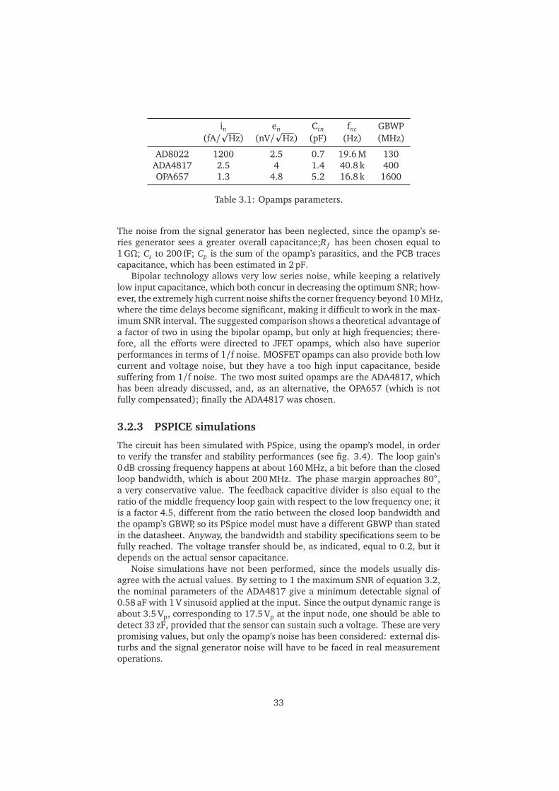
in en Cin fnc GBWP(fA/p
Hz) (nV/p
Hz) (pF) (Hz) (MHz)
AD8022 1200 2.5 0.7 19.6 M 130ADA4817 2.5 4 1.4 40.8 k 400OPA657 1.3 4.8 5.2 16.8 k 1600
Table 3.1: Opamps parameters.
The noise from the signal generator has been neglected, since the opamp’s se-ries generator sees a greater overall capacitance;R f has been chosen equal to1 GΩ; Cs to 200 fF; Cp is the sum of the opamp’s parasitics, and the PCB tracescapacitance, which has been estimated in 2 pF.
Bipolar technology allows very low series noise, while keeping a relativelylow input capacitance, which both concur in decreasing the optimum SNR; how-ever, the extremely high current noise shifts the corner frequency beyond 10 MHz,where the time delays become significant, making it difficult to work in the max-imum SNR interval. The suggested comparison shows a theoretical advantage ofa factor of two in using the bipolar opamp, but only at high frequencies; there-fore, all the efforts were directed to JFET opamps, which also have superiorperformances in terms of 1/f noise. MOSFET opamps can also provide both lowcurrent and voltage noise, but they have a too high input capacitance, besidesuffering from 1/f noise. The two most suited opamps are the ADA4817, whichhas been already discussed, and, as an alternative, the OPA657 (which is notfully compensated); finally the ADA4817 was chosen.
3.2.3 PSPICE simulations
The circuit has been simulated with PSpice, using the opamp’s model, in orderto verify the transfer and stability performances (see fig. 3.4). The loop gain’s0 dB crossing frequency happens at about 160 MHz, a bit before than the closedloop bandwidth, which is about 200 MHz. The phase margin approaches 80,a very conservative value. The feedback capacitive divider is also equal to theratio of the middle frequency loop gain with respect to the low frequency one; itis a factor 4.5, different from the ratio between the closed loop bandwidth andthe opamp’s GBWP, so its PSpice model must have a different GBWP than statedin the datasheet. Anyway, the bandwidth and stability specifications seem to befully reached. The voltage transfer should be, as indicated, equal to 0.2, but itdepends on the actual sensor capacitance.
Noise simulations have not been performed, since the models usually dis-agree with the actual values. By setting to 1 the maximum SNR of equation 3.2,the nominal parameters of the ADA4817 give a minimum detectable signal of0.58 aF with 1 V sinusoid applied at the input. Since the output dynamic range isabout 3.5 Vp, corresponding to 17.5 Vp at the input node, one should be able todetect 33 zF, provided that the sensor can sustain such a voltage. These are verypromising values, but only the opamp’s noise has been considered: external dis-turbs and the signal generator noise will have to be faced in real measurementoperations.
33

1 10 100 1k 10k 100k 1M 10M 100M 1G
-40
0
40
80
120
Loop gain
Voltage transfer
Frequency (Hz)
1 10 100 1k 10k 100k 1M 10M 100M 1G
0
45
90
135
180
Frequency (Hz)
Loop gain
Figure 3.4: Magnitude and phase of voltage transfer and loop gain from PSpicesimulations.
34

+
-
V+
V-
CfC1
A0
C2
-1
Figure 3.5: Differential measurement front-end.
3.3 Inverting buffer
Differential measurements suppress the reference high-swing reference sinu-soid, which does not carry any information, while producing an output signalwhen the sensor’s capacitance varies. With reference to fig. 3.5, and consideringa single pole inverting stage, with time constant equal to τinv , one can derivethe expression of the output voltage as a function of the input voltage and of thecapacitance difference ∆C = C2 − C1:
Vout = Vin
C2
1+ sτinv
− C1
1
C f
= Vin
∆C
C f
(1− sC1/∆Cτinv)
(1+ sτinv)(3.3)
For a perfectly matched couple of sensors (C1 = C2), this equation reduces to
Vout = −Vin
C1
C f
sτinv
1+ sτinv
(3.4)
so only at DC the output is exactly null in that case; by increasing the operativefrequency, the inverting gain gets degraded, and becomes negligible a decadebeyond the buffer’s cutoff frequency (1/(2πτinv), and we return to the singlesensor voltage transfer. If the two sensor are not perfectly equal, due to thepresence of Particulate Matter, or, more likely to the unavoidable manufactur-ing mismatches, a low frequency gain equal to ∆C/C f appears, which can berewritten as:
∆C
C1
C1
C f
(3.5)
This is also the transfer function of the noise from the generator, and it corre-sponds to the single sensor voltage transfer, but with an attenuation equal to therelative matching of the pair of sensor: if a factor of ten attenuation is desired,the two sensors must have a ten percent matching, at least. In order to reducethe noise coming along with the input reference, either the sensor’s absolutevalue has to be as low as possible, and the couple has to be matched. Further-more, if this attenuation must be maintained over the entire frequency range(10 MHz), the pole of the inverting buffer has to be located at least at 100 MHz.
35
100k 1M 10M 100M 1G
-100
-80
-60
-40
-20
0V
olta
ge
tra
nsfe
r (d
B)
Frequency (Hz)
1% matching
∆C=0
Figure 3.6: Voltage transfer function for a differential measurement, for matchedand mismatched sensors.
Figure 3.6 considers two sensors, when perfectly matched, and when matchedat 1%. Being the inverting stage’s pole at 100 MHz, the maximum attenuationwithin the band of interest (10 MHz) still remains of a factor of ten; however,this is not the ultimate limit: if one backs off until 1 MHz, the attenuation be-comes 40 dB with respect to the single sensor measurement, and then it finallystops dropping. The high frequency transfer is −14 dB, the sensors having anaverage value of about 200 fF, and the feedback capacitor being 1 pF.
Of course, this stage must not worsen the overall noise performance of thefront-end. Figure 3.7 shows two possible implementations. A fully differentialinverting configuration, acting as a BalUn, produces a floating voltage refer-ence (3.7a): when everything is perfectly symmetrical, the current recirculatesamong the two sensors; if a capacitive variation happens, a small fraction ofcurrent leaks into virtual ground. It might seem a pleasant solution for its sym-metry, but the fully differential amplifier’s output common mode noise wouldflow entirely into the virtual ground. A simple single-ended inverting stage willbe then employed (3.7b).
The noise contributions will be referred to the opamp’s output voltage, andthen converted into virtual ground current after the sensor’s capacitance. Ther-mal noise from the two resistances is transferred at the output directly; being thetwo sources uncorrelated, a single contribution can multiplied by a factor
p2. A
1 kΩ resistor carries 4 nV/p
Hz, equal to the ADA4817 series noise; however, theformer drops on a capacitance of few hundreds of femto Farad, whilst the latter’drops’ on some pico Farads (see eq. 3.1). If two resistances of 680Ω are cho-sen, their noise contribution is not significant, so we can neglect it. The opamp’s
36

Z
To virtual
ground
A0
Z
ZZ
+
+-
-Cs
Cs
(a) Fully differential.
+
-
V+
V-
R
A0
R
(b) Classic single-ended inverting stage.
Figure 3.7: Two possible implementations of the inverting stage.
series and parallel noise generators, Sv and Si respectively, are transduced intothis current noise at the virtual ground of ADA4817:
Sv(2ωCs)2 + Si(ωRCs)
2
this current should be much lower than the ADA4817 current noise at virtualground:3
Sv,ADA4817ω2(2Cs + Cp + C f )
2
We can neglect the inverter opamp’s current noise, too: common values are ofthe order of 1 pA/
pHz, corresponding to 0.68 nV/
pHzat the inverter output
node. At last this condition must hold:p
Sv <Æ
Sv,ADA4817
1+Cp + C f
2Cs
The right-hand-side of the last inequality is about 48 nv/p
Hz; an opamp with aseries generator of 5 nV/
pHz will be suited for the inverting stage, and this is
just the case for the THS3001, a high speed Current Feedback Amplifier (CFA),having an equivalent input voltage noise of 1.6 nV/
pHz. Actually its negative
input current noise is much more higher with respect to the previous considera-tions, being equal to 16 pA/
pHz; nevertheless, it corresponds to 11 nV/
pHz at
the THS3001 output, or 5.5 nV/p
Hz at its positive input, which fits the specifi-cations.
According to the datasheet, an inverting stage with 680Ω feedback resistorsand ±15V power supply guarantees a −3 dB closed loop bandwidth of about400 MHz. Its 6500 V/µs slew rate allows to work with full power on the entirebandwidth of 10 MHz, as well as the output current is sufficient to drive a 200 fFcapacitive load; the ADA4817 is not limited by output slope issues, too.
3.4 PCB design
The measurement of Particulate Matter will be performed using the basic circuitsdesigned in the previous sections, although some alternatives will be analyzed
3Now the ADA4817 series noise drops on a double sensor capacitance, since the differentialmeasurements employs two equal sensors.
37

later. The acquisition section consists of a bottom board, that accommodatesthe electronics and a custom socket for the sensors slides. Every single slide wasattached on a properly shaped piece of glass fiber substrate (FR-4), which hasthe correct pin arrangement to fit the socket. The sensors slide was bonded tothese pins by means of a silver paste.
The electronics include the transimpedance and the single ended inverter,which have both been terminated with a 50Ω resistor, in order to maintainthe circuit’s stability when driving a capacitive load, and to perform impedancematching with the coaxial cable that reads the circuit’s output. The power sup-ply is external; it has been chosen to ±15 V, so that the inverting stage is ableto provide a high swing reference sinusoid to the sensor. Two voltage regulatorsmust have been added, to shift the power supply level to ±5 V for the ADA4817.The MC79M05 and MC78M05 linear regulators have been chosen. The circuitreceives external power supply, as well as the signal voltage reference, whileproviding the output of the transimpedance, through BNC connectors. Decou-pling capacitors have been added, as suggested by the components datasheets.Two metal jumpers connect the desired electrodes to the voltage references. Thewhole circuit fits a metal box to ensure electrical isolation.
3.5 Resonant front-end
The maximum SNR that can be obtained with the circuit employed so far isdegraded by all the capacitances connected to the non-inverting input of theopamp: the series noise of the active circuit produces a current noise flowinginto the virtual ground; the higher the capacitive admittance, the higher thiscurrent noise (see eq. 3.2). If all these capacitances somehow resonated with aproper inductor, the opamp’s series noise would be applied on an overall infiniteimpedance, and ideally no current noise would flow due to this contribution.
The mentioned inductor should work on the non-inverting voltage transfer,while leaving the signal transfer unchanged, therefore one of its terminals willbe connected to the opamp’s inverting input; this pin must follow the voltageof the non-inverting one thanks to the negative feedback, so the signal’s idealtransfer will be preserved. If we connected the other terminal of the inductordirectly to ground, it would behave as a short circuit at low frequency, thusdeleting the feedback at the bias point. The simplest way to save the feedbackat low frequency might be a bypass capacitor in series with the inductor (seefig. 3.8). This capacitor must be large enough that within the band of interest itbehaves like a very low impedance, so the series is dominated by the inductor.
The ideal voltage noise transfer function to the output node can be thenevaluated:
1+R f /(1+ sR f C f )
sL/(1+ sL(Cp + Cs)=
=1+ sL/R f + s2 L(C f + Cp + Cs)
sL/R f (1+ sR f C f )
The equivalent transadmittance to the virtual ground is obtained:
38

+
-
V+
V-
Cf
Rf
Cs
A0
CLCp
L
Figure 3.8: Transimpedance with inductor.
1+ sL/R f + s2 L(C f + Cp + Cs)
sL
When the inductor resonates with the sum of all the capacitances connectedto the inverting input (some pico Farad), the current noise spectral density isminimized. The feedback resistance limits the quality factor of the resonance,being the ultimate impedance on which the voltage replicated at the invertednode drops; if R f were infinite, no current noise would flow into virtual grounddue to the opamp’s series noise. Anyway, in this case the residual current noisewould be white, and of the order of atto Ampere per root-Hertz, so the otherwhite current noise sources would be the main contributions. There would besome improvements, indeed, for the 20 dB/dec rising part of the virtual groundcurrent noise would be eliminated (fig. 3.3), and the SNR would rise by increas-ing the frequency along the entire bandwidth of interest.
Actually, that is not so immediate. One must also consider that a real inductorhas a limited quality factor, and it works properly only below its antiresonancefrequency. The latter drawback is equivalent to say that the inductor has a para-sitic capacitance, that dominates its impedance above the antiresonance. Theseparasitics must not, of course, be larger than the capacitances that are intendedto be made resonate. The limited inductor’s quality factor can be associated toan equivalent parallel resistance RL
4; following the same previous procedure,the virtual ground transadmittance becomes:
4If the inductor’s losses are represented by a parallel resistance, its quality factor can be expressedas RL/(ωL).
39

1+ sL
1R f
+ 1RL
+ s2 L(C f + Cp + Cs)
sL
This is a quite satisfactory (and predictable) result: the passive elements com-pose themselves in parallel, and so does the overall quality factor, so that thelower one limits the resonance goodness.
The stability of this circuit is a rather tedious task: let’s first calculate thecircuit’s loop gain. The inductor’s series capacitance must now be included,to take into account all the singularities. Its quality factor will be consideredinfinite, instead. The opamp’s transfer function is A(s).
Z f =R f
1+ sR f C f
Zp =1+ s2 LCL
sCL
||1
s(Cp + Cs)=
1+ s2 LCL
s(Cp + Cs + CL) + s3 LCL(Cp + Cs)
Gloop =−A(s)Zp
Zp + Z f
=−A(s)(1+ sC f R f )(1+ s2 LCL)
1+ sR f (C f + Cp + Cs + CL) + s2 LCL + s3 LCLR f (Cp + Cs + C f )
If we consider that Cs and Cp are in parallel in the loop gain calculation, fourreactive elements are present, but a third order transfer has been obtained. Infact, two capacitors are linearly dependent. At low frequency the inductor is inseries with a capacitor, which high impedance; all the capacitors see R f , so thecoefficient of the first degree term is the one expected; the low frequency timeconstant is almost equal to R f CL , since CL dominates the other capacitances.At higher frequencies, we can neglect the 1 at the denominator, and gathersR f CL , obtaining the expression of two complex poles resonance frequency at
ω0 = 1/Æ
L(Cp + Cs + C f ), and quality factor R f /(ω0 L). The loop gain has alsothree zeros: one is due to the feedback parallel RC, while the two remainingare a purely imaginary pair that nullify the loop gain at the LC series resonantfrequency (the circuit closed loop gain is far different from the ideal one aroundthis frequency, since the feedback is null).
The circuit has been simulated with PSpice, and the corresponding frequencyresponses are shown in fig. 3.9. The ADA4817 has been used again, with all thesame parameters as in the integrator section; the inductor has been chosen equalto 100 H, in order to be able to resonate with some pico Farad at a reasonablefrequency, between 1 and 10 MHz; a series capacitor of 2.5 nF resonates withthe inductor at 320 kHz, which seems far enough from the operating frequency.With this choice, the loop gain is high enough at low frequencies in order to setthe bias condition within a reasonable time interval.
The results show that the loop gain stays over 20 dB up to 10 kHz, so thebias is preserved. Around that frequency, the opamp’s first pole makes it de-crease, until, just at 300 kHz, the LC series becomes a short circuit, forcing itto zero. The inverting gain, which is related to the signal’s transfer, stays at itsideal value of −14 dB within the band of interest, except around the LC seriesresonance, where it also drops to zero. The loop gain has finally an antireso-nance at 7.5 MHz: the inductor is resonating with the smaller capacitances. Atthe same frequency, the transadmittance from the non-inverting input to virtual
40

1 10 100 1k 10k 100k 1M 10M 100M 1G
-120
-80
-40
0
40
80M
ag
nitu
de
(d
B)
Frequency (Hz)
Loop gain
Inverting gain
Transadmittance
Figure 3.9: PSpice simulations of the resonant circuit proposed; the magnitudeof loop gain, closed loop gain, and noise transfer to virtual ground are compared.
ground displays a notch behavior. These graphs have been taken sampling at100 points per decade. If the rate is increased to 10 000 in the decade of inter-est, the simulator gives a minimum of 4.9 nS, which is closer to the expectedvalue with respect to what shown on figure 3.9.
The stability of this circuit must be ensured. Unfortunately, the loop gain dis-plays multiple crossings of the 0 dB ax, therefore Bode’s stability criterion cannotbe used. Nyquist’s criterion has to be applied. Figure 3.10 is a plot of the Nyquistdiagram of Gloop( jω) traced with MATLAB. The control theory’s approach willbe followed, so, for negative feedback, a positive low frequency loop gain willbe considered, while the minus sign is included into the differentiator node ofthe feedback block diagram. Since there are no poles with positive real part, thenumber of loops made by the Nyquist diagram around the point (-1,0) must bezero to have stability [16].
The Nyquist diagram never seems to enter the negative real part semi-plane,therefore it should not encircle the (-1,0) point, and the system should be stable(fig. 3.10a). However, scale is very large, so the diagram will be better analyzedwith more detailed pictures to ensure the circuit is truly stable. The diagramstarts at point (36000 ,0), the loop gain at DC (fig. 3.10b). The low frequencypole curves it such that the magnitude diminishes, approaching the origin witha −90 phase (fig. 3.10c). The feedback impedance’s zero stops the middlefrequency magnitude at 14, while bringing the phase back to zero (fig. 3.10c).The opamp’s first pole creates a secondary circular bending, which would bringthe magnitude towards zero with −90, again; the diagram actually crosses theorigin, due to the imaginary zeros pair, which also boost the phase to 90 (fig.3.10d). This phase shift is nullified by the following complex poles pair, witha large magnitude increase that produces the outer ring (fig. 3.10e and 3.10f).
41

−0.5 0 0.5 1 1.5 2 2.5
x 106
−1.5
−1
−0.5
0
0.5
1
1.5x 10
6 Nyquist Diagram
Real Axis
Imagin
ary
Axis
(a) The whole Nyquist diagram lays entirely in thepositive real part semi-plane.
−2 −1 0 1 2 3 4 5 6 7
x 104
−4
−3
−2
−1
0
1
2
3
4
x 104
System: LReal: 3.58e+004Imag: −2.95e+003Frequency (rad/s): 0.033
Nyquist Diagram
Real Axis
Imagin
ary
Axis
(b) It starts at (36000,0).
−20 0 20 40 60 80 100 120 140
−80
−60
−40
−20
0
20
40
60
80
System: LReal: 14.1Imag: −5.09Frequency (rad/s): 3.31e+003
Nyquist Diagram
Real Axis
Imagin
ary
Axis
(c) The zero fixes the middle frequency gain.
−2 −1 0 1 2 3
−2.5
−2
−1.5
−1
−0.5
0
0.5
1
1.5
2
2.5
System: LReal: 9.61e−010Imag: −3.11e−008Frequency (rad/s): 2e+006
Nyquist Diagram
Real Axis
Imagin
ary
Axis
(d) The loop gain crosses the origin when the LC seriesresonates.
−0.5 0 0.5 1 1.5 2 2.5
x 106
−1.5
−1
−0.5
0
0.5
1
1.5x 10
6
System: LReal: 2.65e+003Imag: 7.89e+004Frequency (rad/s): 4.66e+007
Nyquist Diagram
Real Axis
Imagin
ary
Axis
(e) The magnitude increases with 90 phase.
−3000 −2500 −2000 −1500 −1000 −500 0 500 1000 1500 2000
−3000
−2000
−1000
0
1000
2000
System: LReal: 0.54Imag: −367Frequency (rad/s): 4.73e+007
Nyquist Diagram
Real Axis
Imagin
ary
Axis
(f) The complex poles pair produces the outer ring.
Figure 3.10: Nyquist diagram of the resonant circuit’s loop gain.
42

en Cgs C f IDSS Vp
(nV/p
Hz) (fF) (fF) (mA) (V)
MX-20B 1.6 0.6 50 9 -2MO-16 1.5 1.2 30 14 -3
Table 3.2: Parameters of two low-noise JFET, for ID=5 mA, Vsub=−7.5 V,Vgs=−0.2 V.
The diagram ends with a −90 phase, approaching the origin as a single poletransfer, an absolutely stable situation.
One could now object that the opamp has more singularities, that change thediagram. This is true, but the second pole is located at 400 MHz, where the mag-nitude is well inferior than 1, so its effect is definitely negligible. This circuit hasproven its stability, and it seems to be able to significantly reduce the front-endnoise, while substantially keeping the same signal transfer, at least theoretically.Only an effective implementation may confirm all these expectations.
3.6 External JFET front-end
In section 3.2 the transimpedance had a JFET input opamp, to exploit the ben-efits of that technology on noise and input capacitance. The same (or a better)result may be reached by a two stage amplifier, consisting of an external, singletransistor, ultra low noise JFET preamplifier, followed by an ordinary opamp.The preamplifier would determine the noise performances, since the opamp’ssources would be reduced by the first stage’s gain (a factor of ten); on the otherhand, the opamp is needed to increase the overall open loop gain, in order tomake the feedback stronger.
Table 3.2 lists the parameters of two JFETs by MOXTEK, Inc. Both voltagenoise and input capacitance are better than the ADA4817. They also provide avery low feedback capacitance pin, that would desensitize the following stage’snoise even better. And that is actually the whole feedback capacitance, becauseno parallel resistor must be inserted to fix the bias condition, for a reset pin is alsoavailable. This reset pin acts as a diode, and it activates when a negative voltageis applied, sinking current out from the gate terminal (see fig. 3.11). The circuitexhibits a negative feedback, so the drain voltage follows the opamp’s invertingpin, thus fixing the drain current. The n-JFET has a reverse-bias gate currentflowing out of the terminal; if we left only the capacitive network, this wouldcause the output of the opamp to linearly decrease, until it would reach thenegative supply. With a negative reset diode, the gate bias current can flow intoit, keeping the output within the dynamic range. At the same time, the diodemust not absorb the signal current, so the output is low-pass filtered before beingfed back to the reset pin. This bias current is less than 1 pA, corresponding to ashot noise of 0.56 fA; the reset diode small signal resistance is VT/ID, equal to25 GΩ.
The capacitances at virtual ground that concur in the voltage noise transferare now Cs (200 fF), Cgs (600 fF), and C f (50 fF); due to the negative feedback,the drain node remains practically constant, so the gate-drain capacitance does
43

Cs
A0
+
-
V+
V-
Cgs
Cf
CLP
RLPRL
V+
VD
Negative
reset pin
Figure 3.11: Transimpedance with low noise JFET.
not experience the Miller effect, and its value is negligible with respect to thegate-source one if the transistor operates in the saturation region. The 2 pFtrace’s capacitance can be avoided if a bare die device is used, bonding the gatepin directly to the sensor, so the overall contribution is 0.85 pF. Having alsoreduced the voltage noise of a factor of 3, the overall improvement in the SNRcould be more than 10.
The bias condition can be fixed as follows: the first stage gain is the ratiobetween the resistor’s static voltage, and the half overdrive of the JFET. For a5 mA drain current, with the substrate at −7.5 V, the gate-source voltage shouldbe −0.2 V; the pinch-off voltage is about −2 V. We obtain a 1.5 V overdrive, sothe drain voltage can be fixed at 5 V for a gain of 13, with a 15 V positive supply.The load resistance should be 2 kΩ, and the transistor is working in saturation.The transistor’s transconductance can be calculated:
gm =2IDSS
Vp
√
√ ID
IDSS
= 6.7mS
The equivalent voltage noise can also be calculated:
en =4kTγ
gm
= 1.3nV/p
Hz
which is consistent with table 3.2.The low pass components can be chosen equal to 1 GΩ and 1 nF for a time
constant of 1 s: an output voltage of 10 V at 1 MHz becomes 10µV, thereforethe diode does not interfere. Actually, this is an open loop approach. We cancompute the external loop gain, considering that the two active stages along
44
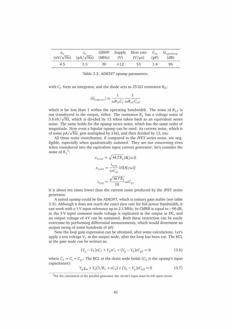
en in GBWP Supply Slew rate Cin Gopenloop
(nV/p
Hz) (pA/p
Hz) (MHz) (V) (V/µs) (pF) (dB)
4.5 1.5 30 ±12 53 1.4 96
Table 3.3: AD8397 opamp parameters.
with C f form an integrator, and the diode acts as 25 GΩ resistance RD:
|Gloop,ex t | ≃1
ωRDC f
1
ωRLP CLP
which is far less than 1 within the operating bandwidth. The noise of RLP isnot transferred to the output, either. The resistance RL has a voltage noise of5.6 nV/
pHz, which is divided by 13 when taken back as an equivalent series
noise. The same holds for the opamp series noise, which has the same order ofmagnitude. Now even a bipolar opamp can be used: its current noise, which isof some pA/
pHz, gets multiplied by 2 kΩ, and then divided by 13, too.
All these noise contribution, if compared to the JFET series noise, are neg-ligible, especially when quadratically summed. They are not concerning evenwhen transduced into the equivalent input current generator: let’s consider thenoise of RL
5:en,out =Æ
4kTRL |A( jω)|
en,out =in,eq
ωCgs
10|A( jω)|
in,eq =
p
4kTRL
10ωCgs
It is about ten times lower than the current noise produced by the JFET seriesgenerator.
A suited opamp could be the AD8397, which is unitary gain stable (see table3.3). Although it does not reach the exact slew rate for full power bandwidth, itcan work with a 1 V input reference up to 2.1 MHz; its CMRR is equal to −96 dB,so the 5 V input common mode voltage is replicated at the output at DC, andan output voltage of 4 V can be sustained. Both these restriction can be easilyovercome by performing differential measurements, which would determine anoutput swing of some hundreds of mV.
Now the loop gain expression can be obtained, after some calculations. Let’sapply a test voltage VT at the output node, after the loop has been cut. The KCLat the gate node can be written as:
(Vg − VT )sC f + VgsC1 + (Vg − Vd)sCgd = 0 (3.6)
where C1 = Cs + Cgs. The KCL at the drain node holds (C2 is the opamp’s inputcapacitance):
Vg gm + Vd(1/RL + sC2) + (Vd − Vg)sCgd = 0 (3.7)
5For the calculation of the parallel generator, the circuit’s input must be left open circuit.
45

By merging these two equations, the drain voltage is obtained as a function of thetest voltage; finally the loop gain expression can be highlighted, by multiplyingthe drain voltage for the opamp’s transfer function A(s):
Gloop(s) = −C f
C f + C1 + Cgd(1+ gmRL)
gmRL(1− sCgd/gm)
1+ sRL
(C1+C f )(C2+Cgd )+Cgd C2
C1+C f +Cgd (1+gmRL)
A(s)
The bias network has been neglected, being its singularities at very low frequen-cies. The DC gain, apart from the opamp’s transfer, is a capacitive divider (whichalso includes the equivalent Miller capacitance at the gate node), multiplied bythe gain of the common source stage. The well known right-semi-plane zeroof the common source would be located at 18 GHz, if Cgd were 1/10 of Cgs.The low frequency loop gain equals 93 dB, producing a gain bandwidth prod-uct, with the 300 Hz pole, of 13.4 MHz. The only pole due to the four capacitors(there are two linearly independent meshes, and a pole-zero cancellation in theorigin), whose complete expression has been highlighted, is located at 91 MHz.The 0 dB crossing’s slope would be −20 dB, ensuring the system’s stability.
46
Chapter 4
Circuit characterization
The lock-in measurement will be performed by a commercial device by ZurichInstruments, the HF2LI digital lock-in amplifier. While providing the sinusoidalreference from a DAC, it converts the output of the transimpedance by meansof an ADC; the digitized signal is then demodulated. The transfer and noisefeatures of the analog stage alone will be first discussed, and then the wholesystem will be studied.
4.1 Transfer functions
Measurements of the circuits gain and bandwidth have been obtained by theAgilent E5061B Network Analyzer. Figure 4.1 shows magnitude and phase fre-quency response of the transimpedance and inverting buffer cascade, when a dis-crete 10 pF capacitor is connected at virtual ground. The middle frequency gainis 17 dB, from which a 1.4 pF value for the feedback capacitor can be guessed.Before 150 Hz, the transfer is rising by 20 dB/dec, owing to the feedback re-sistance. The closed loop bandwidth is around 20 MHz, which is lower thanthe simulated value, for the large test capacitance diminishes the loop gain’scrossing frequency; it fully complies the design specification anyway. The mid-dle frequency phase stands at 0, because the signal undergoes two sign inver-sions. A differential measurement with two 10 pF capacitors proves that they arematched within 1%; the red curve follows the differential transfer anticipatedin the design section, with a zero-pole pair, although the pole is due to the tran-simpedance’s limited bandwidth, and not to the buffer’s. The buffer’s frequencyresponse has been measured separately (figure 4.2). It has a −0.6 dB gain, anda 200 MHz bandwidth.
Now that the feedback capacitance is known with accuracy, we can repeatthe same kind of measurement with the coplanar sensors, in order to extracttheir total capacitance, and the system’s maximum bandwidth. Let’s considerthe slide B of wafer 2; the sensor’s name is made according to the layout sec-tion, so electrodes 2B-2d refers to the sensor of wafer 2, slide B, the second ofgroup d, and so on. Each sensor has been connected to the network analyzer’svoltage source, and tested by the transimpedance. The overall voltage trans-fer is shown in figure 4.3; at middle frequency the magnitude is Cs/C f , whereC f = 1.4 pF. The group ’d’ electrodes of slide B have constant gap and length
47

10 100 1k 10k 100k 1M 10M 100M
-60
-40
-20
0
20
40
Frequency (Hz)
10 pF
Differential
10 100 1k 10k 100k 1M 10M 100M
-180
-135
-90
-45
0
45
90
135
180
Frequency (Hz)
10 pF
Differential
Figure 4.1: Transimpedance and inverting buffer cascade measured transferfunction.
48

10 100 1k 10k 100k 1M 10M 100M 1G
-40
-30
-20
-10
0
10
20
Frequency (Hz)
10 100 1k 10k 100k 1M 10M 100M 1G
-180
-90
0
90
180
Frequency (Hz)
Figure 4.2: Inverting buffer measured frequency response.
increasing with code number, so the capacitance should also increase. The dataprove this trend, but this is probably due to the stray capacitances of the traces:electrodes of group "s" have all been designed equal, but they also differ in theirabsolute capacitance. The capacitance measured values at 1 MHz are listed intable 4.1f: though remaining of the order of a few femto Farad, they are higherthan expected after the simulations, therefore the parasitics must be all but neg-ligible. Anyway, the order of magnitude is compliant to the expectations, as wellas the transfer’s shape, which depicts a frequency independent capacitance foralmost every pair, and suggests a −3 dB bandwidth around 70 MHz.
Sensors 2B-1d and 2B-2d, although designed differently, show a very highmatching, so they have been connected to have a common terminal, to be ableto perform differential measurements; the resulting transfer is also shown onfigure 4.3. It does not faithfully reproduce the expected differential transfer, butit displays a minimum plateau region just in the bandwidth of interest, at−26 dBbelow the single transfer, meaning a 4% matching. The lower frequencies rip-ples must not concern: they are orders of magnitude less than the sensor’s abso-lute value. This connection was done whenever two sensor looked sufficientlymatched. The resulting residual capacitance differs from the exact differencebetween them: the soldering operation perturbs the initial capacitance values.
Table 4.1 and table 4.2 list the capacitances, which are generally close forrespective slides of different wafers. The missing values refer to damaged orshort-circuited sensors. This last issue involves every pair with gap equal to2µm, which was the manufacturing resolution.
The gap qualitative dependence has been verified: slides C and D have adecreasing capacitance with a decreasing gap, though the traces length is in-creasing; in slides A this is partially true, because for the furthest pairs, whichhave the longest traces, the capacitance returns to increase.
4.2 Noise
The noise characterization was carried both in time and frequency domain: therms value has been evaluated with a lock-in filtering around the frequency ofinterest (1 MHz for most of the cases); at the same time the Agilent N9020A
49

Sensor |Gain| Cs (fF)
1A-1s 0.384 5381A-2s 0.346 4851A-3s 0.339 4741A-2s3s 0.013 18
1A-1d / /
1A-2d’ 0.538 7531A-2d” 0.507 7101A-3d 0.146 2051A-4d’ 0.131 1841A-4d” / /
1A-5d / /
(a) Slide 1A.
Sensor |Gain| Cs (fF)
1B-1s / /
1B-2s / /
1B-3s / /
1B-1d / /
1B-2d 0.143 2151B-3d 0.160 2391B-4d / /
1B-5d 0.223 2231B-2d3d 0.008 11
(b) Slide 1B.
Sensor |Gain| Cs (fF)
1C-1s / /
1C-2s 0.349 4881C-3s 0.301 421
1C-1d / /
1C-2d 0.165 2311C-3d 0.118 1651C-4d 0.107 1511C-5d 0.108 151
(c) Slide 1C.
Sensor |Gain| Cs (fF)
1D-1s 0.318 4451D-2s 0.290 4071D-3s 0.291 4081D-2s3s 0.011 15
1D-1d / /
1D-2d 0.192 2691D-3d 0.146 2051D-4d 0.137 1931D-5d 0.136 1911D-4d5d 0.023 33
(d) Slide 1D.
Sensor |Gain| Cs (fF)
2A-1s / /
2A-2s 0.302 4242A-3s 0.284 398
2A-1d / /
2A-2d’ / /
2A-2d” / /
2A-3d 0.136 1902A-4d’ 0.115 1622A-4d” 0.126 1772A-5d 0.139 1942A-2d-diff / /
2A-4d-diff 0.014 19
(e) Slide 2A.
Sensor |Gain| Cs (fF)
2B-1s 0.329 4612B-2s 0.288 4042B-3s 0.249 349
2B-1d 0.115 1602B-2d 0.116 1622B-3d 0.123 1732B-4d 0.147 2052B-5d 0.180 2512B-1d2d 0.006 8.4
(f) Slide 2B.
Table 4.1: Sensor capacitance derived from voltage transfer.
50

Sensor |Gain| Cs (fF)
2C-1s 0.336 4702C-2s 0.345 4832C-3s 0.294 412
2C-1d / /
2C-2d 0.159 2222C-3d 0.111 1552C-4d 0.098 1372C-5d 0.097 135
(a) Slide 2C.
Sensor |Gain| Cs (fF)
2D-1s 0.342 4782D-2s 0.303 4252D-3s 0.297 4162D-2s3s 0.012 17
2D-1d / /
2D-2d / /
2D-3d 0.147 2062D-4d 0.135 1892D-5d 0.133 1862D-4d5d 0.024 34
(b) Slide 2D.
Sensor |Gain| Cs (fF)
4A-1s 0.331 4974A-2s 0.292 4384A-3s 0.253 379
4A-1d 0.188 2824A-2d’ 0.133 1994A-2d” 0.128 1924A-3d 0.115 1614A-4d’ 0.116 1624A-4d” 0.129 1814A-5d 0.152 2274A-2d-diff 0.006 9.454A-4d-diff 0.013 19.0
(c) Slide 4A.
Sensor |Gain| Cs (fF)
4B-1s 0.346 5194B-2s 0.308 4624B-3s 0.255 383
4B-1d 0.128 1924B-2d 0.129 1944B-3d 0.159 2394B-4d / /
4B-5d 0.222 3334B-1d2d 0.001 1.5
(d) Slide 4B.
Sensor |Gain| Cs (fF)
4C-1s 0.348 5224C-2s 0.304 4574C-3s 0.299 4484C-2s3s 0.017 24
4C-1d / /
4C-2d 0.164 2464C-3d 0.115 1724C-4d 0.103 1554C-5d 0.106 1584C-4d5d 0.008 11
(e) Slide 4C.
Sensor |Gain| Cs (fF)
4D-1s 0.314 4394D-2s 0.285 3994D-3s 0.285 3994D-2s3s 0.013 19
4D-1d / /
4D-2d 0.188 2644D-3d 0.141 1974D-4d 0.129 1814D-5d 0.127 1774D-4d5d 0.025 34
(f) Slide 4D.
Table 4.2: Sensor capacitance derived from voltage transfer.
51

10 100 1k 10k 100k 1M 10M 100M
-50
-40
-30
-20
-10
0M
ag
nitu
de
(d
B)
Frequency (Hz)
2B-1s
2B-2s
2B-3s
2B-1d
2B-2d
2B-1d2d
2B-3d
2B-4d
2B-5d
Figure 4.3: Frequency response of the front-end connected to the slide 2B sen-sors.
IN range (Vp) 0.001 0.01 0.1 1
en (nV/p
Hz) 5 5 9 60
Table 4.3: HF2LI lock-in AC coupling input voltage noise.
MXA Spectrum Analyzer has been employed to measure the noise spectral den-sity. The expected rms voltage noise at transimpedance output , with no sensorconnected, should be:
vrms,out = en,ADA4817
1+Cp
C f
pBW = 4nV/
pHz
1+2 pF+ 1.4 pF
1.4pF
p
1kHz
the first factor corresponding to the output voltage spectral density (13.7 nV/p
Hz),producing a 0.43µV noise on the signal’s bandwidth. The HF2LI lock-in alsocarries its own input-referred noise, which varies according to the selected in-put voltage range (see table 4.3). As long as this instrument will be employed,the voltage range is quite limited: in order to keep its noise negligible, the max-imum reference voltage amplitude should be 300 mV with a single sensor mea-surement. The amplitude can be increased if differential measurement are per-formed; in this case a lower input range can be selected, keeping the lock-ininput noise at its minimum.
At first, a characterization of the lock-in itself has been done: a time do-main voltage waveform after lock-in filtering was recorded, keeping the HF2LIinput short-circuited, and then the rms value was calculated (see fig. 4.4). Themeasurements confirm the data on the user’s manual (table 4.4). Then, thetransimpedance was connected to the HF2LI, but still with no sinusoid applied(table 4.5), and with its virtual ground open-circuited. The datum at 1 MHz isvery close to the expectations; at higher frequency the lock-in input capacitance
52

21130 21140 21150 21160
-20,0n
-15,0n
-10,0n
-5,0n
0,0
5,0n
10,0n
15,0n
20,0n
Vo
lta
ge
(V
)
Time (s)
IN range 0.98mV
Figure 4.4: Voltage waveform after lock-in filtering, with reference frequency of1 MHz, noise equivalent bandwidth of 1.1 Hz, and short circuited input port (INrange of 0.98 mV).
Frequency Bandwidth IN range Voltage rms en
(MHz) (Hz) (V) (nV) (nV/p
Hz)
1 1.1 0.98 m 4.80 4.361 1.1 81 m 8.60 7.821 1.1 130 m 12.3 11.21 1.1 0.98 45.5 41.41 1.1 2 76.3 69.4
Table 4.4: HF2LI lock-in input voltage noise, measured for different inputranges.
53

Frequency Bandwidth IN range Voltage rms en
(MHz) (Hz) (V) (nV) (nV/p
Hz)
10 1.1 0.98 m 15.4 14.01 1.1 0.98 m 19.1 17.4
0.1 1.1 0.98 m 46.5 42.30.01 1.1 0.98 m 153 139
1 1.1 81 m 20.7 18.81 1.1 130 m 27.7 25.21 1.1 0.98 53.3 48.41 1.1 2 86.8 78.9
Table 4.5: Transimpedance output voltage noise.
Frequency Bandwidth IN range Voltage rms Circuit(MHz) (Hz) (V) (nV)
1 1.1 0.98 m 24.4 B, 1A-2s, T1 1.1 0.98 m 21.7 B, 1A-1s, T1 1.1 0.98 m 25.0 1A3s, T1 1.1 0.98 m 22.7 1A1s, T
Table 4.6: Transimpedance, buffer, and sensors output voltage noise (B=buffer,T=transimpedance).
acts as a filter, so the 10 MHz value is not useful. At lower frequencies the noiseshould increase, due to the 1/f contributions, and the white current noise of theopamp. If higher input ranges are chosen, the noise also increases, accordingly.If the inverting buffer is added, along with a sensor, the overall noise does notshow a significant worsening (table 4.6). The spectral analysis confirms the timemeasurements (fig. 4.5). The low frequency noise is 4µV/
pHz, i.e. the ther-
mal noise of a 1 GΩ resistor. At about 100 Hz the feedback capacitance becomesmore conductive, therefore the white current noise gets integrated; the drop isnot infinite: at high frequency the opamp’s voltage noise is transferred to theoutput, according to the non-inverting gain. The measured curve is slightly dif-ferent from the theoretical one, since the slope is a bit less than −20 dB/dec,and also the high frequency plateau is about 20 nV/
pHz, which is higher than
expected, although very close. Actually, below 100 kHz, the opamp produces asignificant amount of 1/f voltage noise, with a 3 dB corner frequency at 10 kHz.According to the opamp’s datasheet, the 1/f slope is −10 dB/dec up to 100 Hz,beyond which it becomes steeper. The 1/f noise has been included in the theo-retical spectrum, and R f was also considered in the feedback impedance, givingthis formula:
e2n,out
=R2
f
1+ (ωR f C f )2
¨
Si +4kT
R f
+1+ [ωR f (C f + Cs + Cp)]
2
R f
Sv
1+ωnc
ω
«
where Sv and Si are the opamp white noise power spectral densities. By lookingat figure 4.5, 1/f noise contribution is not visible even in the theoretical spec-trum, so it is unlikely to be the cause of the different shape around 100 kHz.
54

Measured
TheoreticalV
olta
ge
no
ise
sp
ectr
al d
en
sity (
V/√
Hz)
Frequency (Hz)
Figure 4.5: Measured voltage noise spectral density at the output node of thetransimpedance.
Anyway, the overall trend is compliant with the theory, and beyond 1 MHz thespectral density is comparable to the expected value, proving to be the mostsuitable working frequency interval.
At this point the overall measurement setup, including the sinusoidal refer-ence provided by the HF2LI, must be tested: this final analysis led to a verydisappointing result. The noise contribution from the signal generator, whichhad always been neglected in the previous sections, turned out to be the maincontribution (see table 4.7).
According to the lock-in user’s manual, the output DAC that provides the si-nusoidal reference should carry a 25 nV/
pHz white voltage noise, which drops
on a 500 fF sensor capacitance in the worst case, according to the previous mea-surements; the sum of all the capacitances at virtual ground, which determinethe opamp’s contribution to the overall noise, are ten times higher; the equiv-alent DAC noise at the opamp’s non-inverting pin is 2.5 nV/
pHz, therefore it
should be negligible. The first row of table 4.7, instead, shows a value morethan two orders of magnitude higher when the sensor is stimulated by the lock-in voltage reference. The second row shows a differential measurement with thesame other parameters: the noise drops significantly (about 20 times), althoughthe spectral density is still too much intense; this proves it must come along withthe voltage reference. The third row deals, again, with a single sensor measure-ment, having reduced the reference by 1/12; the resulting noise dropped by1/6, so this noise is amplitude dependent. We can see it also in rows 5 and 6:when the amplitude is scaled by 5, the noise diminishes by 4. One last consider-ation: when the lock-in low pass bandwidth gets 1000 times higher (row 2 and6), the noise does not increase by
p1000, (more or less a factor of 30), but much
55

Ref voltage BW IN range Voltage rms en,eq Circuit(V) (Hz) (V) (nV) (nV/
pHz)
1 1.1 2 8279 7526 1A1s, T1 1.1 2 410 373 B, 1A2s3s, T
81 m 1.1 2 1380 1254 1A1s, T1 1.1 81 m 319 290 B, 1A1s2s, T5 1 k 56 m 5746 179 B, 4B1d2d, T1 1 k 14 m 1437 45 B, 4B1d2d, T
0.1 1 k 4.7 m 812 25 B, 4B1d2d, T
Table 4.7: Output voltage noise with sinusoidal reference; the first column refersto the voltage amplitude of the signal at the DAC output; all the measurementswere taken at 1 MHz.
less. Therefore, white noise is not being measured. The fifth column displays anequivalent noise spectral density, which has been evaluated by dividing the rmsvalue by the square root of the bandwidth, as if it were white noise.
These observations suggest that phase noise is being measured. A spectralanalysis of the voltage reference from the HF2LI is shown in figure 4.6a. Threedifferent amplitudes have been analyzed: 1 V, 100 mV, and 10 mV. The typicalphase noise sidebands are clearly visible; the ratio to the carrier peak is constant,for a given frequency deviation: when the amplitude scales by ten, the sidebandalso decreases by 20 dB, indicating that this noise is directly proportional to thesignal’s amplitude. The amount of phase noise affecting a sinusoidal signal isidentified by the Single Sideband to Carrier Ratio (SSCR), which is the ratio ofthe noise power (in a bandwidth of 1 Hz), at a certain frequency deviation ωm
from the carrier ω0, to the carrier power. It results that SSCR(ωm) = Sφ/2,where Sφ is the phase noise spectral density [15]. The HF2LI user’s manualindicates a −120 dBc phase noise for a 1 kHz deviation from 10 MHz (integratedover a 0.67 Hz bandwidth). Figure 4.6a is consistent with such a description,and it explains the excessive noise measured. The sidebands cannot decreasebelow the white noise floor, which is actually higher than 25 nV/
pHz. Figure
4.6b makes a comparison with the spectrum of a waveform generator by Agilent;the two are quite the same, so it looks useless to demand better performancesto a signal generator.
The most critical aspect about phase noise is the proportionality with thevoltage sinusoid amplitude. The SNR does not increase any more with the volt-age, as long as the phase noise is dominant. One may ask why phase noise isconcerning in a lock-in demodulation: if the two sinusoids at the multiplier’sinputs share the same zero crossing fluctuations, they are always synchronous,and no phase noise should be detected. The HF2LI generates the sinusoidal ref-erence relying on the digital samples stored in its registers, which get convertedinto a continuous waveform by a Direct Digital Synthesizer (DDS) along with theDAC. This analog sinusoid gets corrupted by phase noise, and, after the signalacquisition operations, it is read by the HF2LI input ADC, and finally demodu-lated into digital domain. The digital reference sinusoid does not experience thesame corruption, so a net phase fluctuation arises.
The reference signal’s noise was also studied using the lock-in itself (table
56

Vo
lta
ge
sp
ectr
al d
en
sity (
V/√
Hz)
Frequency (Hz)
1V
100mV
10mV
(a) Spectrum of the voltage reference from HF2LI lock-in, for different amplitudes.
Vo
lta
ge
sp
ectr
al d
en
sity (
V/√
Hz)
Frequency (Hz)
Zurich HF2LI
Agilent 33522A
(b) Comparison between HF2LI output and agilent 33522A waveform generator.
Figure 4.6: Spectrum of the reference sinusoid.
57

Ref BW IN range Voltage rms en,eq OUT range Notes(V) (Hz) (V) (nV) (nV/
pHz) (V)
1 1.1 2 26720 25476 11 1.1 2 156 148 1 Diff1 1.1 2 17329 16504 1 Diff, 2 gen
0.1 1.1 2 2207 2012 10.1 1.1 2 81 77.1 1 Diff0.1 1.1 0.13 1960 1867 10.1 1.1 0.13 1930 1838 0.1
10 m 1.1 0.13 219 208 0.11 m 1.1 0.13 41 39 10 m1 m 1.1 2 240 228 10 m1 1.1 81 m 15126 14406 1 Diff, 2 gen1 1.1 81 m 67.4 64.2 1 Diff1 20 2 29365 6566 11 1 k 2 33809 1069 11 1.1 2 23496 22377 1 33522A1 20 2 28254 6318 1 33522A1 1 k 2 35512 1123 1 33522A1 1.1 2 35811 34106 1 81150A1 1.1 2 185 176 1 81150A, Diff
Table 4.8: HF2LI output waveform noise; all the measurements were taken at1 MHz.
4.8), by connecting the DAC output directly to the ADC input. In a 1 Hz band-width, the spectral density is about 25µV for a 1 V signal. When the amplitudeis scaled by ten, also the noise scales by the same factor, coherently with figure4.6a. To decrease the phase noise at its minimum, the amplitude was scaledto 1 mV, and the input range had to be reduced to 130 mV, otherwise the ADCinput noise would have dominated (row 10 and 11); we see that the DAC whitenoise floor is about 40 nV/
pHz, which is also compliant with figure 4.6a.
This bottom limit is not a realistic situation, because with such a low voltagethe optimum SNR would get 1000 times worse. A differential measurement isnecessary to significantly reduce the reference signal’s noise. The HF2LI inputscan read differential signals, so the noise rejection was tested by splitting thesame output DAC to a differential input. As expected, the noise experienced asubstantial reduction, even though it did not reach the noise limit of the ADCinput range. A similar differential measurement was also performed: this timetwo different DAC outputs were sent to the same ADC differential input (row 3);a very weak attenuation was seen, perhaps indicating some correlation betweenthe two output channels. If the noise bandwidth is increased, the rms value isnot proportional to its root square, as already pointed out; it is not white noise.
The HF2LI allows to lock an external sinusoidal reference to an internal PLL,and to use it as a demodulation reference. Two external waveform generatorsby Agilent were tested, the 33522A and the 81150A. The external sinusoid wasthen sampled by the ADC, and also locked to the internal PLL, so that it would beused as a lock-in reference. Ideally, the two signals at the inputs of the multiplier
58

should be exactly the same, and no phase noise should be detected; actually, ta-ble 4.8 shows an unchanged situation, the external generators providing phasenoise performances similar to the internal one’s. After all, the ultimate phasenoise source is the internal clock of the lock-in, whose jitter corrupts all thediscrete-time stages; the sampled external waveform must be processed by thedigital PLL, before it becomes the lock-in reference, so it might experience fur-ther clock jitter with respect to the sampled input; therefore, there is no way tocancel this phase noise with this kind of approach. The same holds if the DAC’soutput were reread to provide a more reliable reference.
4.3 System sensitivity
The most important result from the previous analysis is that the voltage genera-tor noise limits the system’s resolution. A differential measurement is mandatoryto reach an acceptable SNR. The transimpedance output noise, with a 1 V ref-erence, can be successfully lowered with a pair of differential sensors, providedthat their matching is high; table 4.5 displays a factor of 20 noise attenuationbetween row 1 and 2; raising the voltage amplitude proves useless to the SNR.For a 1 kHz bandwidth, the output rms voltage noise can be 1.4µV, which corre-sponds to a capacitive signal of 2.1 aF. If a margin is taken on the SNR, a 10 aFsignal should be detectable with confidence.
59

Chapter 5
PM detection
5.1 Measurement approach
In the horizontal flow measurement, particulate matter is confined in a layer offluid, subject to laminar flow. The motion is not perfectly horizontal, for the par-ticle tends to drop with a sedimentation speed, which results from the balance ofthe all forces applied: gravity and viscous friction (the lift force can be neglectedfor these parameters values). In steady state condition, the sedimentation speedis equal to
vz =2
9
r2
µ(ρp −ρ f )g
for a spherical particle, where r is the radius, µ is the fluid’s viscosity, ρp andρ f are the volumic masses of the particle and of the fluid, g is the gravitationalacceleration. A 10µm plastic sphere has a 3 mm/s sedimentation speed. Thehorizontal speed vx was indicatively set to 1 mm/s; therefore such a particlewould immediately drop, instead of proceeding horizontally. If the diameter ishalved, the sedimentation speed becomes 1/4 (still comparable to vx), but theexpected capacitive signal, less than 1 aF for a plastic sphere, decreases belowthe system’s sensitivity. With diameters close to 1µm the vertical speed wouldbe sufficiently low, but the current sensitivity cannot reach such values.
The particle’s speed might be increased to handle a vertical speed of 3 mm/s.The minimum length to be traveled on a single sensor is about 100µm; if thevertical drop must be limited within 1µm, the horizontal speed should not getbelow 300 mm/s. From the pulse shape section we recall that the spatial widthof a pulse is of the order of 10µm, corresponding to a 30µs duration. Such asignal would require a 33 kHz lock-in bandwidth, a factor of 5.72 higher thanthe current value. The minimum detectable capacitance would become 12 aF,preventing even the 10µm particle from being detected.
The sedimentation speed also depends on the fluid’s density. This issuewould be easily overcame by choosing a liquid medium, e.g. water. Water has a1000 times higher volumic mass, providing a sufficient buoyancy to keep the par-ticles on flow. Nevertheless, in-water measurements are commonly performed.We will try to measure PM in air, because it would be a much more importantresult.
60

11200 11400 11600 11800 12000 12200 12400-19100
-19080
-19060
-19040
-19020
-19000
-18980
-18960
C
apacitance [
aF
]
Time [s]
∆C = 73aF
Figure 5.1: Capacitive signal due to a 20µm plastic bead.
This compromise between measurement feasibility and resolution can beovercome by choosing a vertical fall approach: the particles would drop on thesensor, so even a steady state, narrow bandwidth measurement could be accom-plished.
5.2 Static measurements
Static measurements have been carried out by positioning with accuracy sin-gle particles on a sensor; the corresponding capacitance steady state value hasbeen compared to the initial value, thus measuring a variation. The circuit wasplaced on a microscope, which allowed to track the particle while it was beingpositioned, and to take pictures of the sensing area. Plastic beads of known di-ameter and permittivity (2.6) have been used; the lock-in bandwidth was set to1.1 Hz, since steady state values had to be measured.
At first, 20µm diameter beads were measured. The 4A4d’4d” differentialpair was chosen. The conversion gain between the sensor’s capacitance and theoutput voltage is
Cs =C f
A0Vout
Since the lock-in displays the output rms voltage, an additionalp
2 factor mustbe included:
Cs =1.4 pF
1V
p2Vout,rms
61

Of course, since the voltage transfer is a capacitive ratio, the lock-in demodulatesreal part of the output voltage.
Figure 5.1 shows the detected signal: three steady state intervals are visible;they are separated by high frequency signals, caused by the metal probe used toposition and to remove the beads. A capacitive increase of 73 aF was measured,after two sticked beads had been placed in the middle of the 10µm gap of sensor4A4d’, which is one of the two sensors forming the 4A4d triple. After the beads’removal, the sensor’s capacitance got back to its initial value. Two pictures havebeen taken: after the beads’ positioning (fig 5.2a), and after the removal (fig5.2b). One bead is just in the middle of the gap, while the other is a bit outside;after the removal, they are still visible at the upper edge of the triple, far awayfrom the gap. The signal’s polarity is consistent with the arrangement: the upperelectrode of the triple receives the negative voltage reference, while the lowerone receives the positive. Since the initial capacitance value is negative, thelower sensor must be greater than the upper one, because the transimpedancethat follows has a negative gain. The capacitive signal tends to reduce the abso-lute value of the overall capacitance, therefore the upper electrodes must haveincreased their value duo to the presence of the particles, which is just the case.To further validate this measurement, a simulation of the sensor was done, withone 20µm plastic sphere touching the surface. The returned value is 42 aF for asingle bead in the middle of the gap, in perfect agreement with the experimentalresult.
The second test dealt with 10µm plastic beads (see fig. 5.4), placed on thetriple 1A2d’d”. This time a negative variation of 40 aF was detected. The sim-ulation of a 10µm bead above a 4µm gap predicts 25 aF. At first no beadswere present above the gap of the triple 1A2d (fig. 5.4a), that is the upper one;unfortunately, the manufacturing process failed to produce the electrodes withaccuracy in this case, because they clearly show some unwanted ripples; thisworsened the matching of the triple, resulting in a poor attenuation. Some cir-cular dark defects in the gap area are visible, but they can be well distinguishedby the spherical, transparent beads in the nearby. In the second picture (fig.5.4b), a group of four beads appears above the upper gap, but only two seem tobe in the sensitive volume, so the measured signal agrees with the simulation.In the third picture (fig. 5.4c), the group of beads has been removed; the onlyones visible are not on the gap, and the measured capacitance gets back to theinitial value. Again, the polarity is correct: the initial value is negative, so theupper couple, which receives the positive voltage reference, has a greater capac-itance; when the beads are present, the measured value becomes more negative,therefore the upper pair’s capacitance increased. The system has proven to beable to detect PM10.
5.3 Dynamic measurements
An air suspension of industrial talc was created by means of an aerosol machine.This talc powder has an average 8µm aerodynamic diameter, on a log-normaldistribution, with 60% of the total being finer of 10µm; it is composed by MgOfor the 31.5 %, and by Si02 for the 62.5 %, whose permittivities are equal to 4 and9, respectively. The particles were injected into a PDMS chamber, as depictedin figure 5.5. The inlet, decentralized from the sensors area, allowed only a
62

(a) The two spheres are in the middle of the gap of sensor 4A4d’.
(b) The two spheres have been removed from the gap.
Figure 5.2: Pictures of the microscope image of sensor 4A4d’4d” during 20µmspheres detection.
63

2400 2450 2500 2550 2600
-45760
-45740
-45720
-45700
-45680
-45660
-45640
Ca
pa
cita
nce
(a
F)
Time (s)
Figure 5.3: Capacitive signal due to a 10µm plastic bead.
thin, mono-particle layer of talc to reach the active electrode pair, with a certainconcentration. The particles deposition was sensed in real time, so a minimum100 Hz lock-in bandwidth was chosen.
The differential pair 2B-2s3s was used at first. The measurement results arelisted in table 5.1; the net capacitive signal is the difference between the sensorsinitial capacitance (for the differential pair 2B-2s3s it equals 14 fF, while for asingle sensor it could be 500 fF), and the steady state value after the aerosol ma-chine was turned off, when all the talc particles settled on the surface. Figure5.6a shows the first measurement: a positive net signal of 100 aF was detected.The transient is characterized by a certain granularity: a series of smaller ca-pacitive steps, either positive or negative, suggest that the talc particles dropquite randomly on both the electrodes; some major steps can be identified, cor-
Attempt Net signal Sensor BW Gap(aF) (Hz) (µm)
1 100 2D-2s3s 100 42 -15 2D-2s3s 100 44 15 2D-2s3s 100 49 -80(x2) 2D-2s3s 1 k 411 -10 2D-2s3s 1 k 412 -100 2D-1s 1 k 418 -170 2D-3d 100 6
Table 5.1: Series of dynamic measurements; the capacitive signal is in goodagreement with the microscope photographs.
64

(a) No beads on electrodes 1A2d.
(b) Four beads in the gap area of electrodes 1A2d’.
(c) The group of beads has been removed.
Figure 5.4: Microscope pictures of the bipolar signal.
65

Air suspended
particles
Figure 5.5: Microfluidic chamber for air suspended particles measurement.
responding to bigger particles; during the transient, even 10 aF steps are visible.The second measurement shows a net 15 aF step, followed by a non-monotone
transient, probably due to the tail of particles which are slower to settle. Mea-sure 4 can be also quantified in a net 15 aF step, but positive. The transientshows two (or three) successive signals, the former rising by 25 aF, the latterdecreasing by 10 aF.
Perhaps the most interesting measurement is number 9. Two, well separated,−80 aF steps can be distinguished; figure 5.7c is a photograph of the electrodes.Two greater grains are visible on the right side of electrode 3s, likely the causeof these two steps. Other smaller particles were spread uniformly, and the con-centration was low enough to distinguish all of them. Figure 5.7b highlights aninner step of −20 aF, right after the first major step.
Measurement number 11 is quite interesting: although the net signal re-mains within 10 aF, the transient displays a series of multiple bipolar signals,which also include some 40 aF steps.
The last two measurements were performed with a single electrode, there-fore without input noise reduction. The initial capacitance is now of the orderof hundreds of fF, and signals of hundreds of aF were measured.
The minimum detected signal was 10 aF, lower than the signal produced bya single 10µm bead during the static measurements; the dielectric constant oftalc powder is also higher than polystyrene’s, so we may conclude that particleswith diameter lower than 10µm were detected.
5.4 Conclusions
The design of this particulate matter detector ended successfully. Two remark-able accomplishments can be highlighted: it has been proven that particulate
66

1037,0 1037,5 1038,0 1038,5 1039,0
14360
14380
14400
14420
14440
14460
14480
14500
14520
14540
14560
14580
14600
Ca
pa
cita
nce
(a
F)
Time (s)
(a) Measure 1.
3051 3052 3053 3054 3055 3056 3057 3058
14520
14530
14540
14550
14560
14570
14580
Ca
pa
cita
nce
(a
F)
Time(s)
(b) Measure 2.
3032 3033 3034 3035 3036 3037
14470
14480
14490
14500
14510
14520
Ca
pa
cita
nce
(a
F)
Time (s)
(c) Measure 4.
Figure 5.6: Sensor capacitance after lock-in demodulation.
67

3925,5 3926,0 3926,5 3927,0 3927,5
13760
13800
13840
13880
13920
13960
14000
14040
14080
Ca
pa
cita
nce
(a
F)
Time (s)
(a) Measure 9.
3926,06 3926,08 3926,10 3926,12 3926,14
13880
13900
13920
13940
13960
13980
14000
14020
14040
14060
Ca
pa
cita
nce
(a
F)
Time (s)
(b) Measure 9 (detail).
(c) Measure 9 (electrodes).
Figure 5.7: Sensor capacitance after lock-in demodulation.
68

6059,0 6059,5 6060,0 6060,5 6061,0
14300
14320
14340
14360
14380
14400
14420
14440
14460
Ca
pa
cita
nce
(a
F)
Time (s)
(a) Measure 11.
7270 7272 7274 7276 7278
-510,8
-510,7
-510,6
-510,5
Ca
pa
cita
nce
(fF
)
Time (s)
(b) Measure 12.
860 865 870 875 880 885 890 895 900
-224,45
-224,40
-224,35
-224,30
-224,25
-224,20
-224,15
-224,10
-224,05
-224,00
-223,95
Ca
pa
cita
nce
(fF
)
Time (s)
(c) Measure 18.
Figure 5.8: Sensor capacitance after lock-in demodulation.
69

matter can be detected by capacitive impedance measurements, the system be-ing able to reveal single particles of the PM10 fraction, at least; it has been proventhat this kind of measurement can be done directly in the air.
The initial goal to build a compact module able to perform the whole mea-surement has not been fully achieved. There are some major issues that makethe single particle counting, with diameter sorting, a difficult task. The hori-zontal flow approach turned out to be impracticable, due to the sedimentationspeed. Only the smaller particles can float adequately, but the current sensitiv-ity cannot sense them. A vertical fall approach was chosen, but the PM2.5 is stillbeyond the system’s capability.
The total sensor capacitance was ignored during the design process, but iteventually emerged as the cause of the input noise transfer, which was the maincontribution in the SNR, because of the phase noise accompanying the voltagereference. After all, there are five or six orders of magnitude between the ca-pacitive signal and the total sensor’s capacitance: the voltage reference has toguarantee a 100 to 120 dB dynamic, which is a quite extreme requirement. Itwould have been much simpler to limit the sensor’s capacitance in the layoutprocess: thinner and shorter electrodes, stray insensitive traces geometry, anddifferential pairs only.
The horizontal flow approach allows to count single particles without los-ing anyone (within the sensitivity limit), because PM has to cross the sensor.Conversely, in the proposed vertical flow approach, the particles are requiredto fall exactly in correspondence of the gap: a consistent fraction gets lost. Ofcourse, the geometry can be optimized to reduce the inefficient area, by adopt-ing interdigitated configurations that cover the whole sensor surface. Or, insteadof capacitive electrodes, a CCD matrix could be an alternative sensor: the PMwould cover a certain number of pixels, also giving direct information on thediameter, and no particle would be lost. Anyhow, the particles dropped on thesensor must be removed in some way, otherwise the surface would saturate. Apossible solution could be the ultrasonic removal.
An integrated sensor along with the acquisition and demodulation stageswill be the next step, thanks to the MEMS technology. The sensor may be addedabove the electronics area, or aside. The integrated manufacturing process pro-vides a higher lithographic resolution, at least 1µm; electrodes separated bya narrower gap could be fabricated, resulting in a higher transduction gain. Ahuge advantage would result by the extreme reduction of parasitic capacitances,allowing to reach the 10 zF sensitivity: the PM2.5 and the sub-micron detectionwould be the next challenges.
An example of successful air microfluidic particulate sorting is described byPapotny et al. [14]. Once the particles have been divided by size, an array ofcustom, parallel-plate sensors would sense them, as was done by Kawaguchi et
al. for 300 nm pollen measurement [17]. Anyway, because of the fluidodynamicissues of the horizontal flow, an interdigitated electrodes array for vertical fallwill be realized, as a first attempt for a fully integrated system.
70

Acknowledgements
I would like to acknowledge my family: my parents Biagio and Ida, and mybrother Federico. They’ve allowed me to live this very important formative ex-perience with the maximum tranquility and freedom, providing the necessaryfinancial support, and always being close to me; this accomplishment wouldhave never been achieved without them; my girlfriend Yelena: besides being ex-tremely encouraging, since I met her, I have changed my point of view on manythings, which also include university, and she is a fundamental part of my lifeand of my choices; Prof. Marco Sampietro, who gave me the opportunity to workon a novel and interesting project, always trusting his students, and making theright decision whenever necessary; Ing. Marco Carminati, who supervised methrough the whole work, establishing a friendly cooperation; Prof. Giorgio Fer-rari, who took part to the project, always sharing a part of his time with whoeverneeded an advice, having everything clear in his mind; Ing. Elena Bianchi, Ing.Francesca Nason, Prof. Luca Cortelezzi (from McGill University), Prof. GabrieleDubini: they designed a reliable micro-fluidodynamic system, which proved tobe very critical; my friends Ema, Caste and Scotti, for the experiances I haveshared and the time I have spent with them, and for that will be spent; my uni-versity mates Ose, Fabio, Paolo, Tiziano, Luca, Pietro, whom I shared this pathwith, the laboratory mates Giacomo, Ibrahim, Davide, Andrea G. and Andrea R.,Giovanni, the researchers Ing. Maddalena Binda and Prof. Dario Natali: I wishthe best to all of them.
71

Bibliography
[1] Zereini F., Wiseman C. L. S., Airborne Particulate Matter: Sources, Composi-
tion and Concentrations, Springer (2010).
[2] Marcazzan G. M., Vaccaro S., Valli G., Vecchi R., Characterization of PM10
and PM2.5 particulate matter in the ambient air of Milan (Italy), AtmosphericEnvironment 35 (2001) 4639–4650.
[3] Basic Guide to Particle Counters and Particle Counting, Particle MeasuringSystems, Inc. (2011).
[4] Baron P. A., Kulkarni P., Willeke K., Aerosol Measurement: Principles, Tech-
niques, and Applications, Wiley (2011).
[5] Ashok A., Barrett S. R. H., Caiazzo F., Waitz I. A., Yim S. H. L. , Air pollution
and early deaths in the United States. Part I: Quantifying the impact of major
sectors in 2005, Atmospheric Environment 79 (2013) 198e208.
[6] Carminati M., Sampietro M., Carminati G., Analysis of Instrumentation Per-
formance for Distributed Real-Time Air Quality Monitoring
[7] Vecchi R., Il particolato atmosferico: la composizione elementare
[8] Carminati M., Instrumentation for electrical detection in biology and nano-
electrochemistry, Doctoral Dissertation (2009).
[9] Meade M., Lock-in amplifiers: principles and applications, IEE electrical mea-surement series, P. Peregrinus on behalf of the Institution of Electrical Engi-neers (1983).
[10] Alagna D., Sistema di Generazione ed Acquisizione con Elaborazione Real-
Time su FPGA per Misure Elettrochimiche, MSc Dissertation (2011).
[11] Carminati M., Ferrari G., Sampietro M., Attofarad resolution potentiostat for
electrochemical measurements on nanoscale biomolecular interfacial systems,Rev. Sci. Instrum. 80, 124701 (2009).
[12] Rottigni A., Electronical instrumentation for impedance measurement on
biosamples, Doctoral Dissertation (2012).
[13] Chen J. Z., Darhuber A. A., Troian S. M., Wagnera S., Capacitive sensing of
droplets for microfluidic devices based on thermocapillary actuation, Lab Chip4 (2004) 473-480.
72

[14] Paprotny I., Doeringa F., Solomonc P. A., Whitea R. M., Gundelb L. A., Mi-
crofabricated air-microfluidic sensor for personal monitoring of airborne par-
ticulate matter: Design, fabrication, and experimental results, Sens. ActuatorsA: Phys. (2013), http://dx.doi.org/10.1016/j.sna.2012.12.026
[15] Lacaita A. L., Levantino S., Samori C., Integrated Frequency Synthesizers for
Wireless Systems, Cambridge (2007).
[16] Bolzern P., Scattolini R., Schiavoni N., Fondamenti di controlli automatici,McGraw-Hill (2008).
[17] Kawaguchi C., Noda T., Tsutsui M., Taniguchi M., Kawano S., Kawaii T.,Electrical detection of single pollen allergen particles using electrode-embedded
microchannels, J. Phys.: Condens. Matter 24 (2012).
[18] Bernardoni V., Vecchi R., Valli G., Piazzalunga A., Fermo P., PM10 source
apportionment in Milan (Italy) using time-resolved data, Science of the TotalEnvironment 409 (2011) 4788–4795.
73