Embed Size (px)
Citation preview
Photolithography:The Basics of Projection Printing
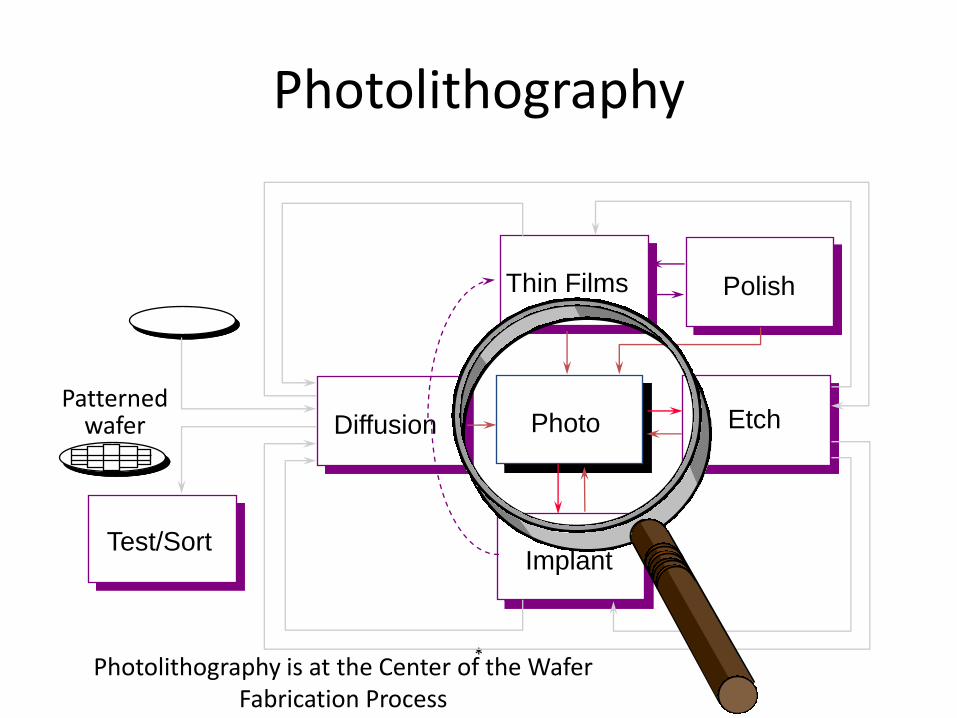
Photolithography
Photolithography is at the Center of the Wafer Fabrication Process
*
Thin Films
Implant
Diffusion Etch
Test/Sort
Polish
PhotoPatterned
wafer
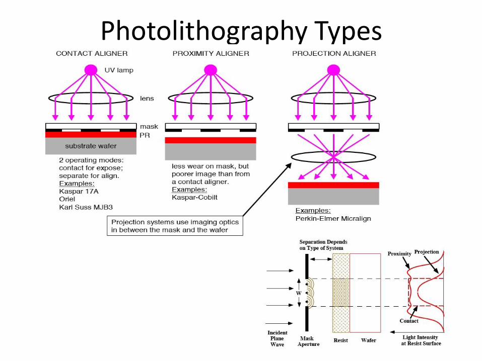
Photolithography Types
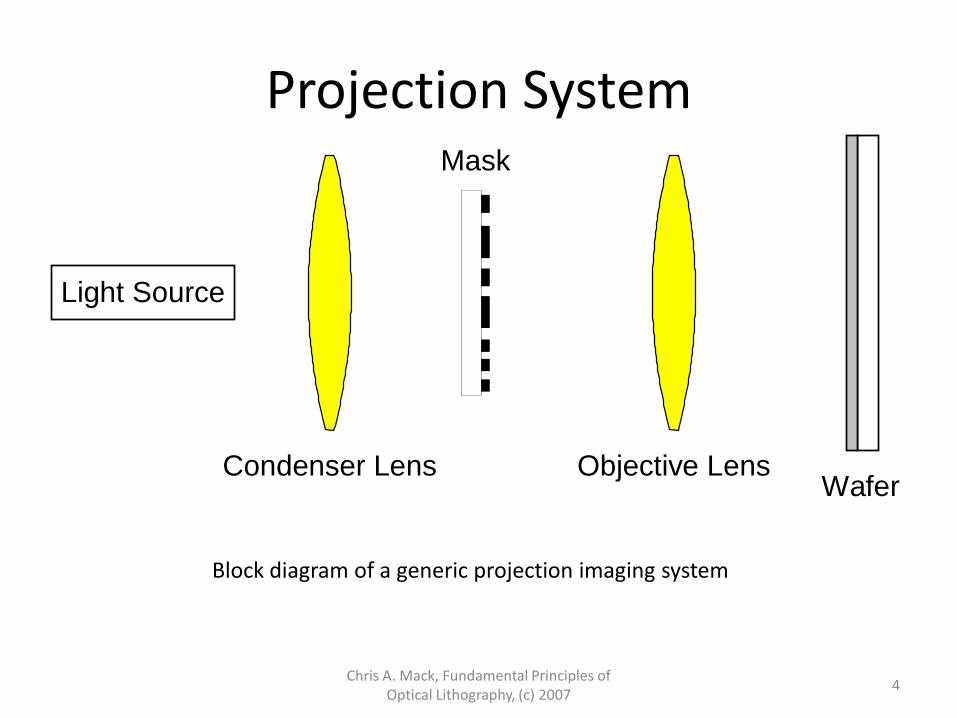
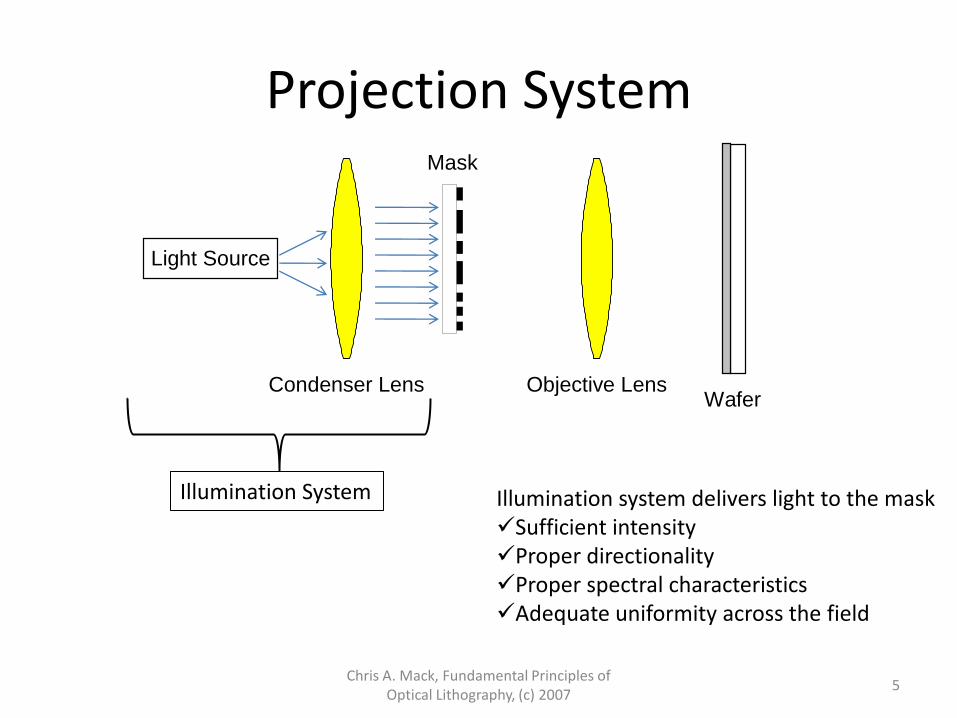
Projection System
Chris A. Mack, Fundamental Principles of Optical Lithography, (c) 2007
4
Light Source
Condenser Lens
Mask
Objective Lens Wafer
Block diagram of a generic projection imaging system
Projection System
Chris A. Mack, Fundamental Principles of Optical Lithography, (c) 2007
5
Light Source
Condenser Lens
Mask
Objective Lens Wafer
Illumination System Illumination system delivers light to the maskSufficient intensityProper directionalityProper spectral characteristicsAdequate uniformity across the field
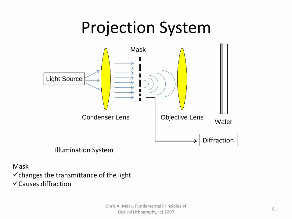
Projection System
Chris A. Mack, Fundamental Principles of Optical Lithography, (c) 2007
6
Light Source
Condenser Lens
Mask
Objective Lens Wafer
Illumination System
Maskchanges the transmittance of the lightCauses diffraction
Diffraction
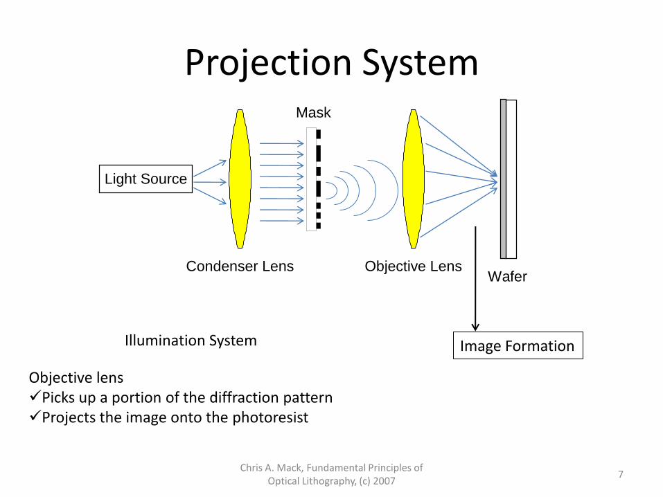
Projection System
Chris A. Mack, Fundamental Principles of Optical Lithography, (c) 2007
7
Light Source
Condenser Lens
Mask
Objective Lens Wafer
Illumination System
Objective lensPicks up a portion of the diffraction patternProjects the image onto the photoresist
Image Formation
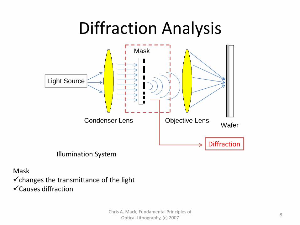
Diffraction Analysis
Chris A. Mack, Fundamental Principles of Optical Lithography, (c) 2007
8
Light Source
Condenser Lens
Mask
Objective Lens Wafer
Illumination System
Maskchanges the transmittance of the lightCauses diffraction
Diffraction
Diffraction
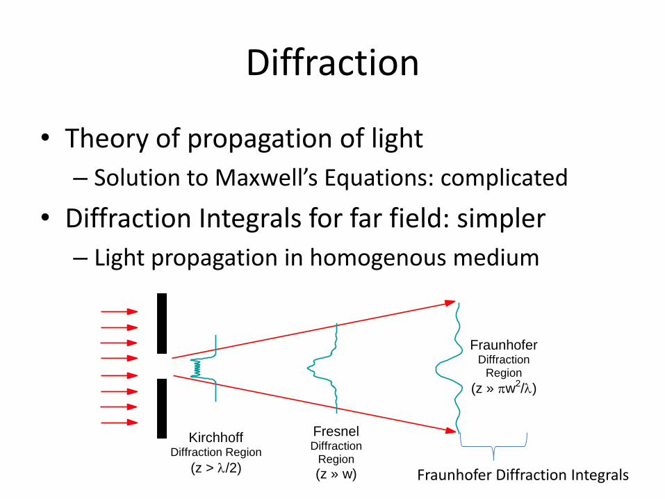
• Theory of propagation of light
– Solution to Maxwell’s Equations: complicated
• Diffraction Integrals for far field: simpler
– Light propagation in homogenous medium
Fresnel Diffraction
Region
(z » w)
Kirchhoff Diffraction Region
(z > /2)
Fraunhofer Diffraction
Region
(z » w2/)
Fraunhofer Diffraction Integrals
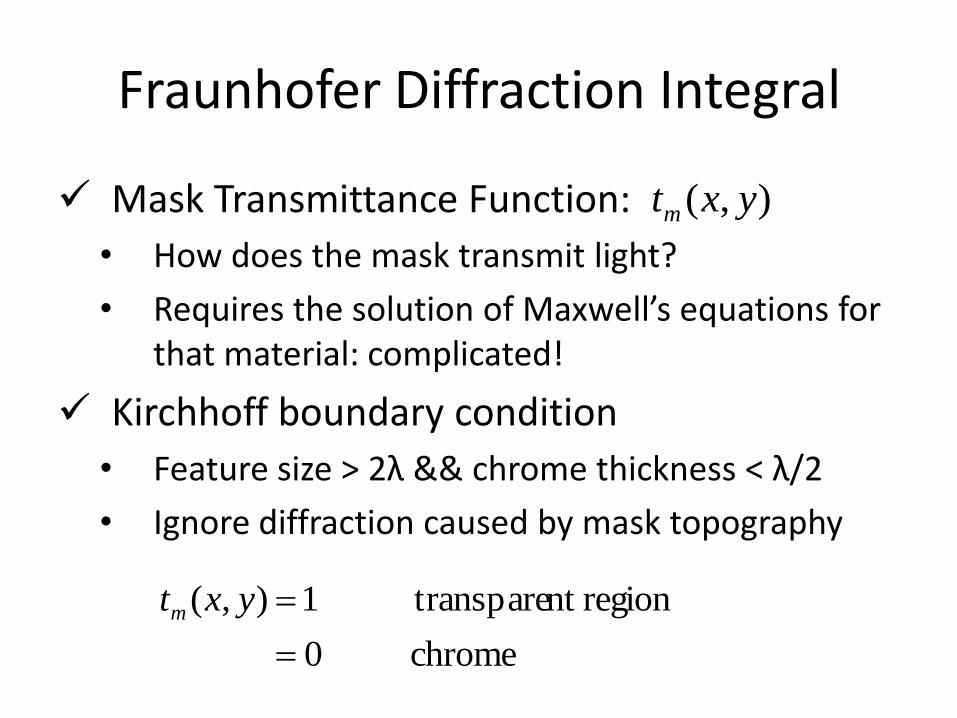
Fraunhofer Diffraction Integral
Mask Transmittance Function:
• How does the mask transmit light?
• Requires the solution of Maxwell’s equations for that material: complicated!
Kirchhoff boundary condition
• Feature size > 2λ && chrome thickness < λ/2
• Ignore diffraction caused by mask topography
),( yxtm
chrome 0
regionnt transpare 1),(
yxtm
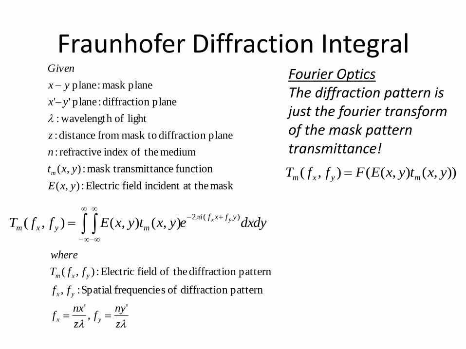
Fraunhofer Diffraction Integral
mask at theincident field Electric : ),(
function mittancemask trans : ),(
medium theofindex refractive :
planen diffractio mask to from distance :
light ofh wavelengt:
planen diffractio :plane ''
planemask : plane
yxE
yxt
n
z
yx
yx
Given
m
dxdyeyxtyxEffTyfxfi
myxmyx )(2
),(),(),(
z
nyf
z
nxf
ff
ffT
where
yx
yx
yxm
',
'
patternn diffractio of sfrequencie Spatial : ,
patternn diffractio theof field Electric : ),(
Fourier OpticsThe diffraction pattern is just the fourier transform of the mask pattern transmittance!
)),(),((),( yxtyxEFffT myxm
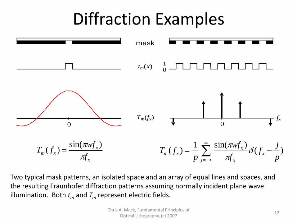
Diffraction Examples
Chris A. Mack, Fundamental Principles of Optical Lithography, (c) 2007
12
fx 0 0
mask
0 1
Tm(fx)
tm(x)
Two typical mask patterns, an isolated space and an array of equal lines and spaces, and the resulting Fraunhofer diffraction patterns assuming normally incident plane wave illumination. Both tm and Tm represent electric fields.
x
xxm
f
wffT
)sin()(
j
x
x
xxm
p
jf
f
wf
pfT )(
)sin(1)(
Chris A. Mack, Fundamental Principles of Optical Lithography, (c) 2007
13
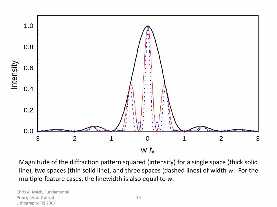
0.0
0.2
0.4
0.6
0.8
1.0
-3 -2 -1 0 1 2 3
w fx
Inte
nsi
ty
Magnitude of the diffraction pattern squared (intensity) for a single space (thick solid line), two spaces (thin solid line), and three spaces (dashed lines) of width w. For the multiple-feature cases, the linewidth is also equal to w.
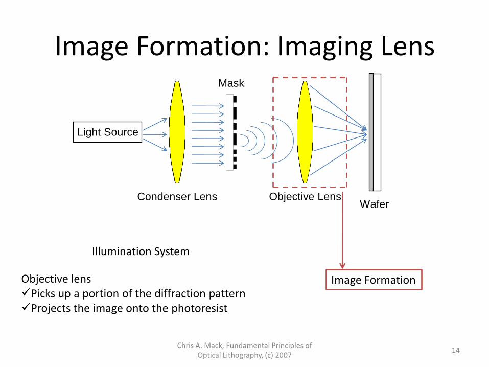
Image Formation: Imaging Lens
Chris A. Mack, Fundamental Principles of Optical Lithography, (c) 2007
14
Light Source
Condenser Lens
Mask
Objective Lens Wafer
Illumination System
Objective lensPicks up a portion of the diffraction patternProjects the image onto the photoresist
Image Formation
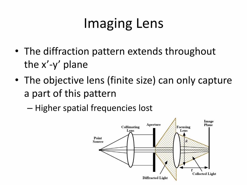
Imaging Lens
• The diffraction pattern extends throughout the x’-y’ plane
• The objective lens (finite size) can only capture a part of this pattern
– Higher spatial frequencies lost
16
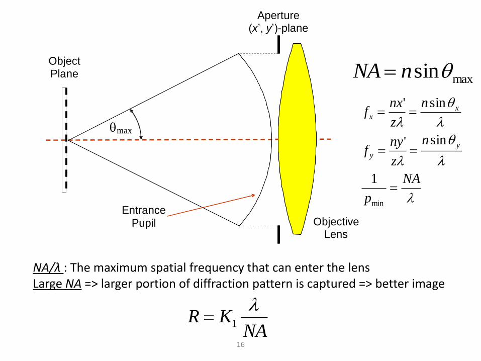
Aperture
(x’, y’)-plane
Object Plane
max
Objective Lens
Entrance Pupil
maxsinnNA
NA
p
n
z
nyf
n
z
nxf
y
y
xx
min
1
sin'
sin'
NA/λ : The maximum spatial frequency that can enter the lensLarge NA => larger portion of diffraction pattern is captured => better image
NAKR
1
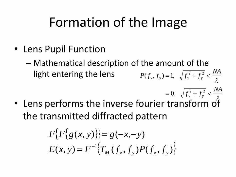
Formation of the Image
• Lens Pupil Function
– Mathematical description of the amount of the light entering the lens
• Lens performs the inverse fourier transform of the transmitted diffracted pattern
NAff
NAffffP
yx
yxyx
22
22
,0
,1),(
),(),(),(
),(),(
1
yxyxM ffPffTFyxE
yxgyxgFF
18
0.0
0.2
0.4
0.6
0.8
1.0
1.2
1.4
-w -w/2 0 w/2 w
Horizontal Position
Re
lative
In
ten
sity
N = 1
N = 3
N = 9
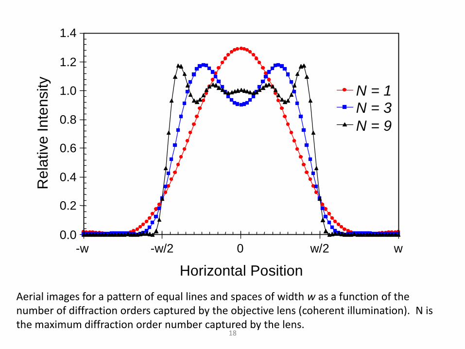
Aerial images for a pattern of equal lines and spaces of width w as a function of the number of diffraction orders captured by the objective lens (coherent illumination). N is the maximum diffraction order number captured by the lens.
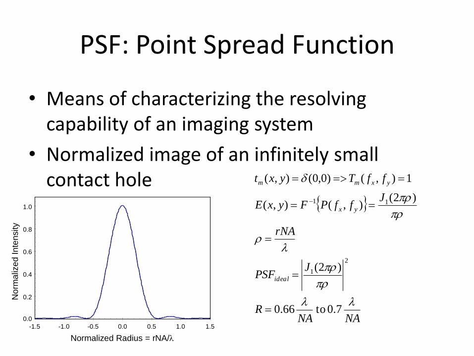
PSF: Point Spread Function
• Means of characterizing the resolving capability of an imaging system
• Normalized image of an infinitely small contact hole
NANAR
JPSF
rNA
JffPFyxE
ffTyxt
ideal
yx
yxmm
7.0 to66.0
)2(
)2(),(),(
1),()0,0(),(
2
1
11
0.0
-1.5 -1.0 -0.5 0.0 0.5 1.0 1.5
Normalized Radius = rNA/
0.2
0.4
0.6
0.8
1.0
No
rma
lize
d I
nte
nsity
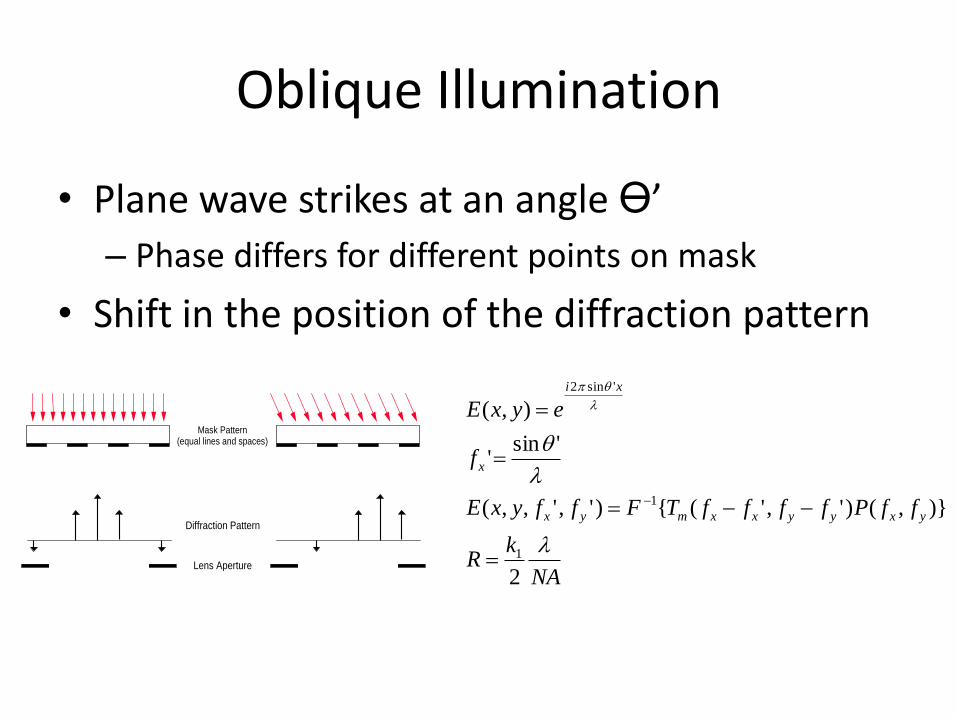
Oblique Illumination
• Plane wave strikes at an angle ϴ’
– Phase differs for different points on mask
• Shift in the position of the diffraction pattern
NA
kR
ffPffffTFffyxE
f
eyxE
yxyyxxmyx
x
xi
2
)},()','({)',',,(
'sin'
),(
1
1
'sin2
Diffraction Pattern
Lens Aperture
Mask Pattern (equal lines and spaces)


![090427 Lecture 9 (Photolithography).ppt [호환 모드]Mask to Wafer Alignment • Alignment: Each mask following the first must be carefully aligned to the previous pattern on the](https://img.pdfslide.us/doc/110x75/613340a7dfd10f4dd73af7c9/090427-lecture-9-photolithographyppt-eeoe-mask-to-wafer-alignment.jpg)