Embed Size (px)
Citation preview
Photolithography Mask Design
Advisor: Dr. Gary Tuttle Daniel O’Connell
Levi Weiss Benjamin Ch’ng
Chen Wen Wang Liao
May 13-25 Photolithography Mask Design
Background: EE432/532
• EE 432/532 is a microelectronics fabrication class – Popular class
• Make a silicon wafer with devices including MOSFET and BJT – in an educational purpose class
• A hands on class with lab at Applied Science Complex – Diffusion – Oxidation – Photolithography
• mask
– Evaporation – And more
May 13-25 Photolithography Mask Design
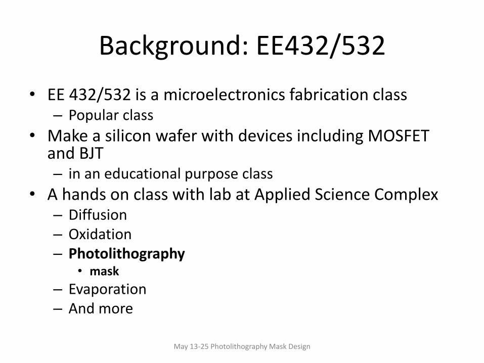
Photolithography
May 13-25 Photolithography Mask Design
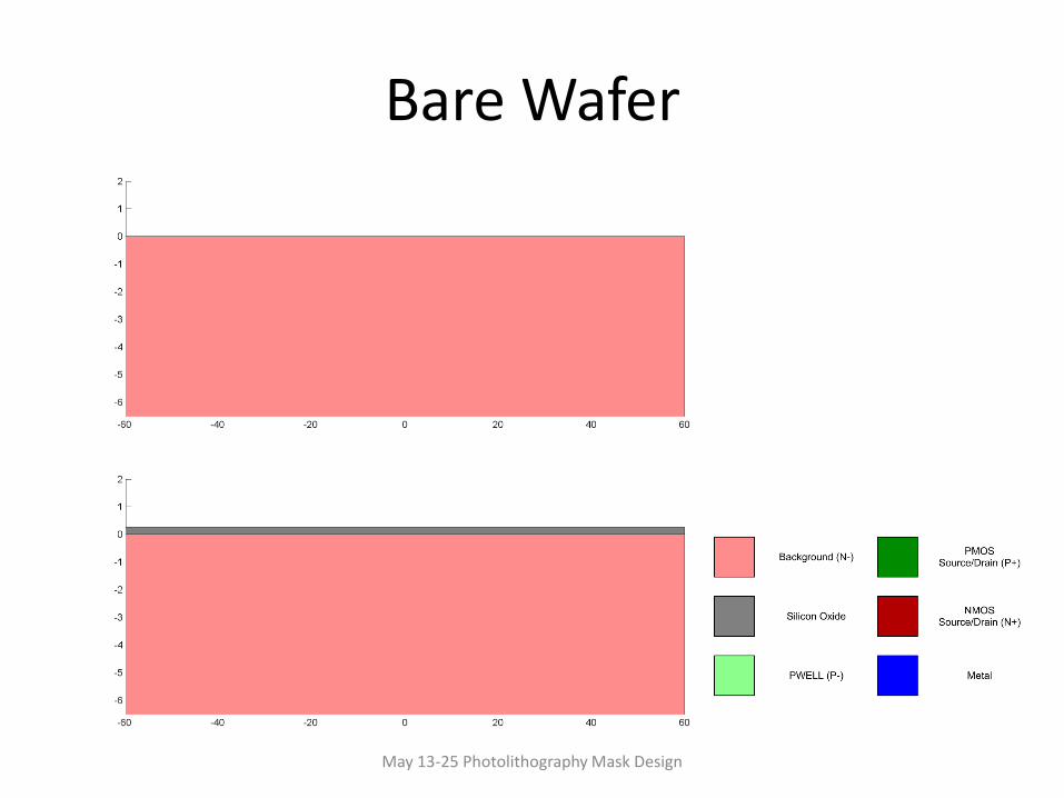
Bare Wafer
May 13-25 Photolithography Mask Design
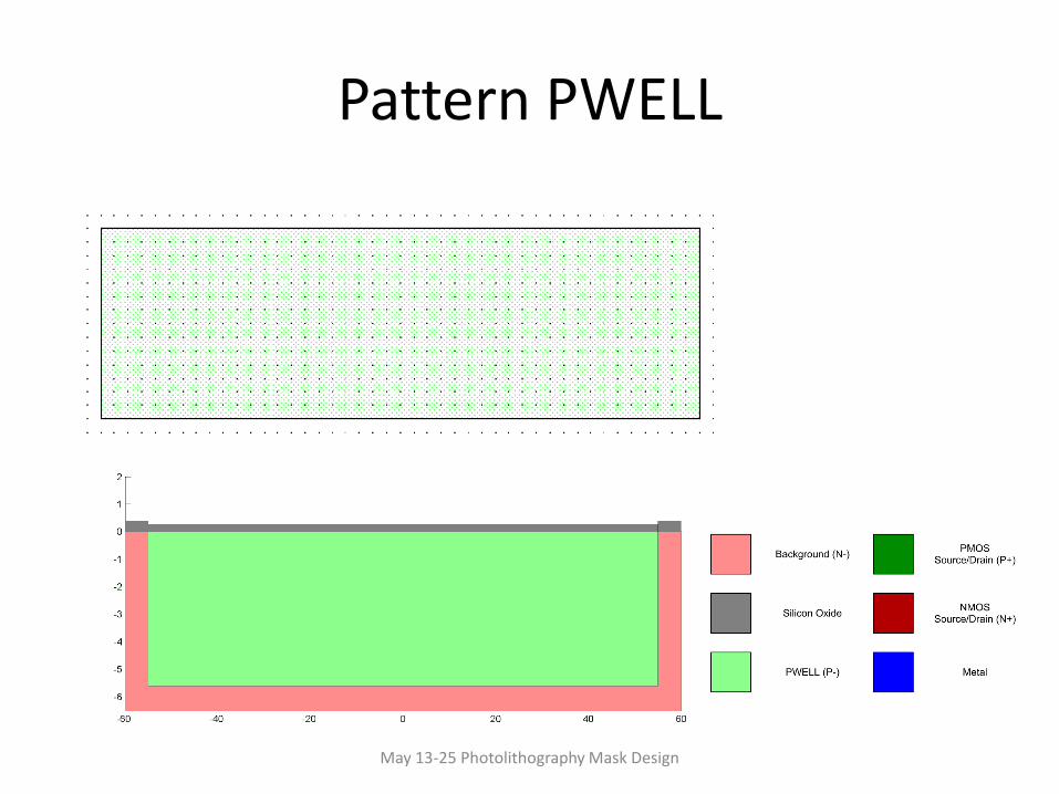
Pattern PWELL
May 13-25 Photolithography Mask Design
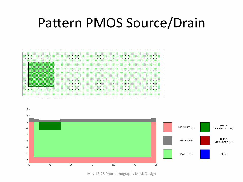
Pattern PMOS Source/Drain
May 13-25 Photolithography Mask Design
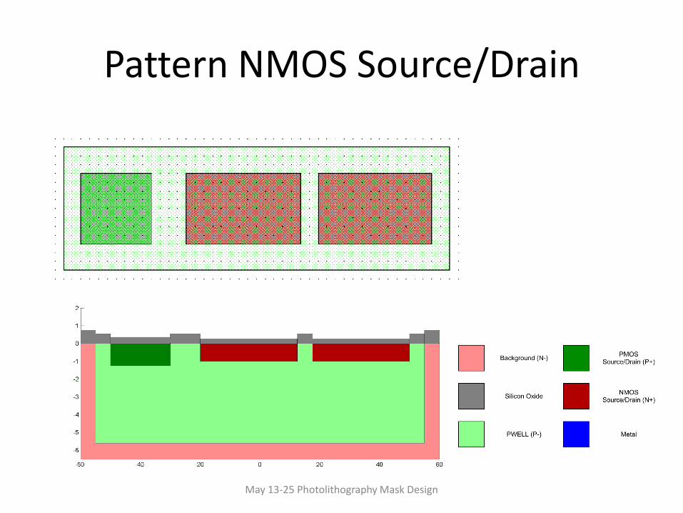
Pattern NMOS Source/Drain
May 13-25 Photolithography Mask Design
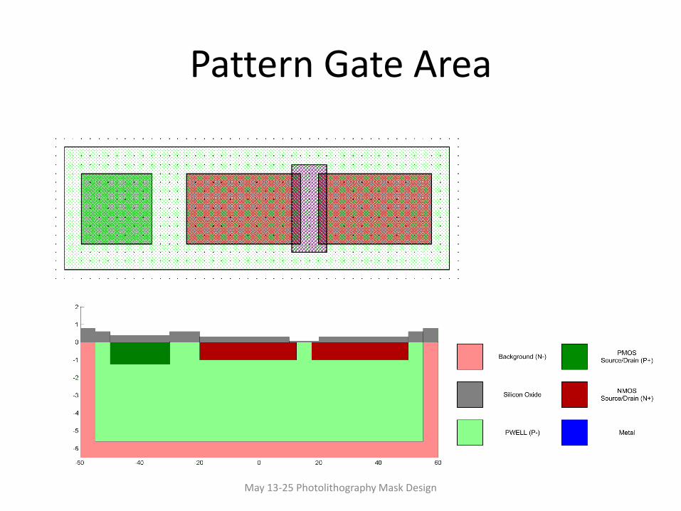
Pattern Gate Area
May 13-25 Photolithography Mask Design
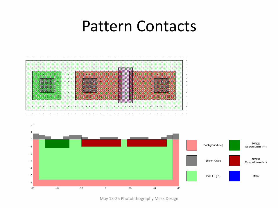
Pattern Contacts
May 13-25 Photolithography Mask Design
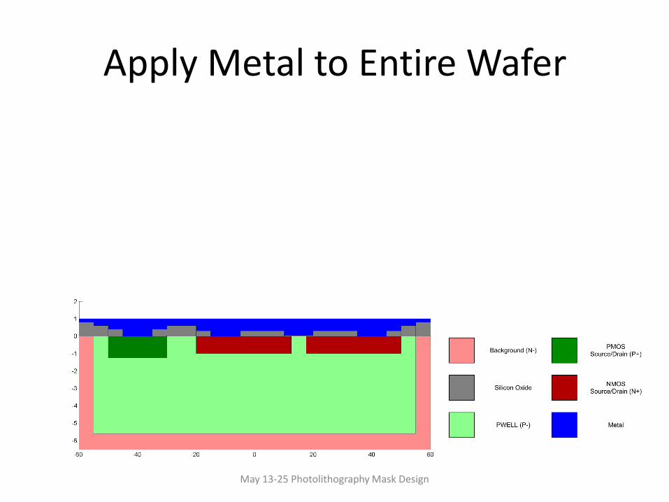
Apply Metal to Entire Wafer
May 13-25 Photolithography Mask Design
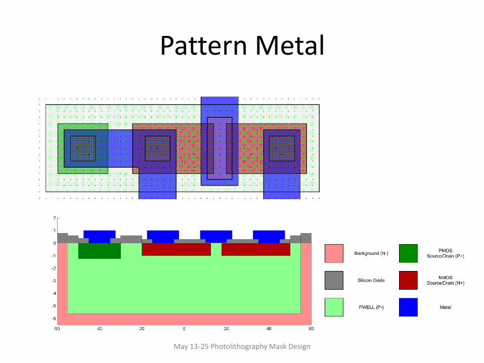
Pattern Metal
May 13-25 Photolithography Mask Design
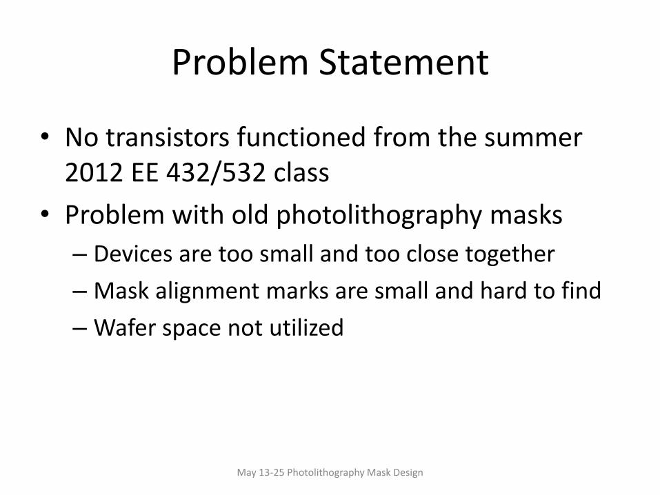
Problem Statement
• No transistors functioned from the summer 2012 EE 432/532 class
• Problem with old photolithography masks
– Devices are too small and too close together
– Mask alignment marks are small and hard to find
– Wafer space not utilized
May 13-25 Photolithography Mask Design
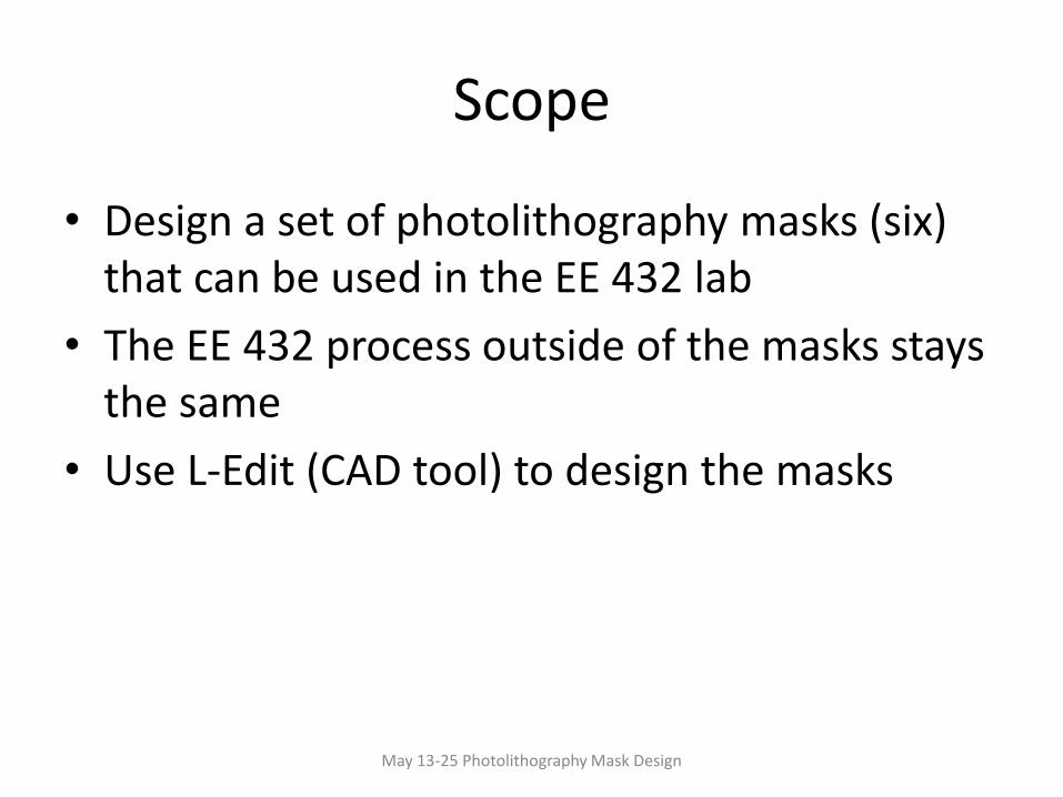
Scope
• Design a set of photolithography masks (six) that can be used in the EE 432 lab
• The EE 432 process outside of the masks stays the same
• Use L-Edit (CAD tool) to design the masks
May 13-25 Photolithography Mask Design
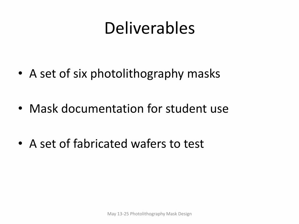
Deliverables
• A set of six photolithography masks
• Mask documentation for student use
• A set of fabricated wafers to test
May 13-25 Photolithography Mask Design
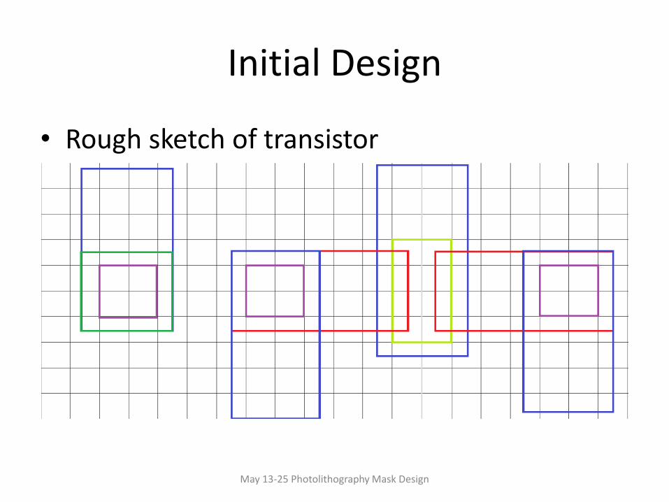
Initial Design
May 13-25 Photolithography Mask Design
• Rough sketch of transistor
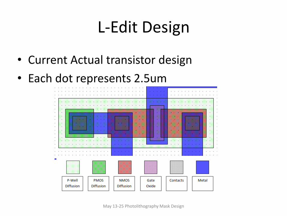
L-Edit Design
• Current Actual transistor design
• Each dot represents 2.5um
May 13-25 Photolithography Mask Design
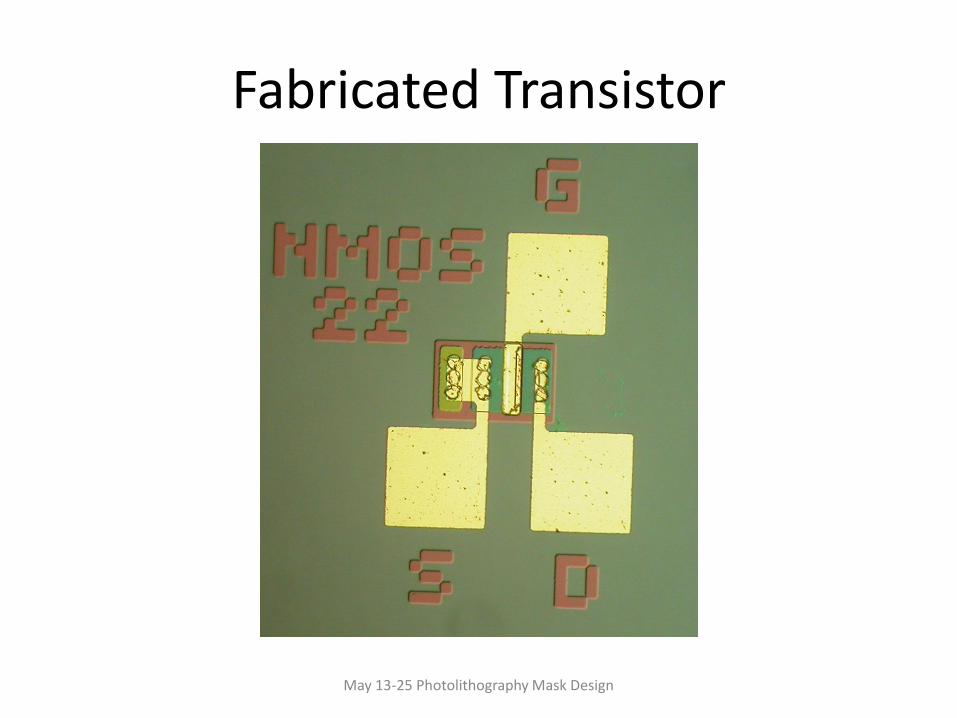
Fabricated Transistor
May 13-25 Photolithography Mask Design
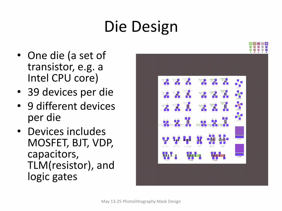
Die Design
• One die (a set of transistor, e.g. a Intel CPU core)
• 39 devices per die • 9 different devices
per die • Devices includes
MOSFET, BJT, VDP, capacitors, TLM(resistor), and logic gates
May 13-25 Photolithography Mask Design
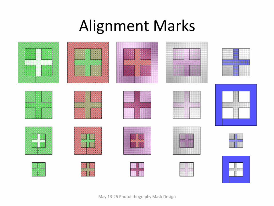
Alignment Marks
May 13-25 Photolithography Mask Design
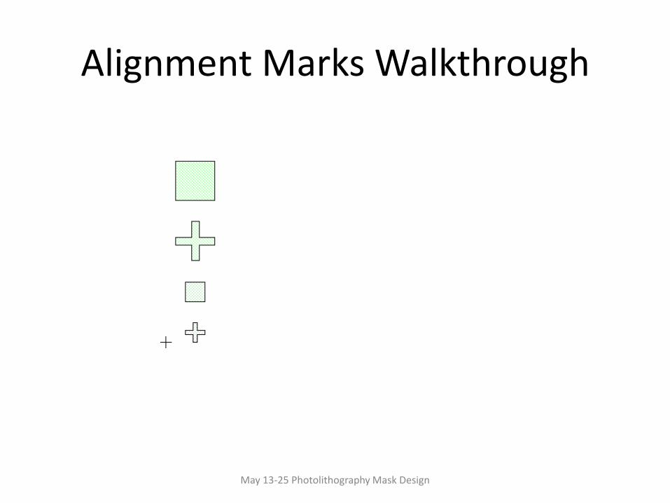
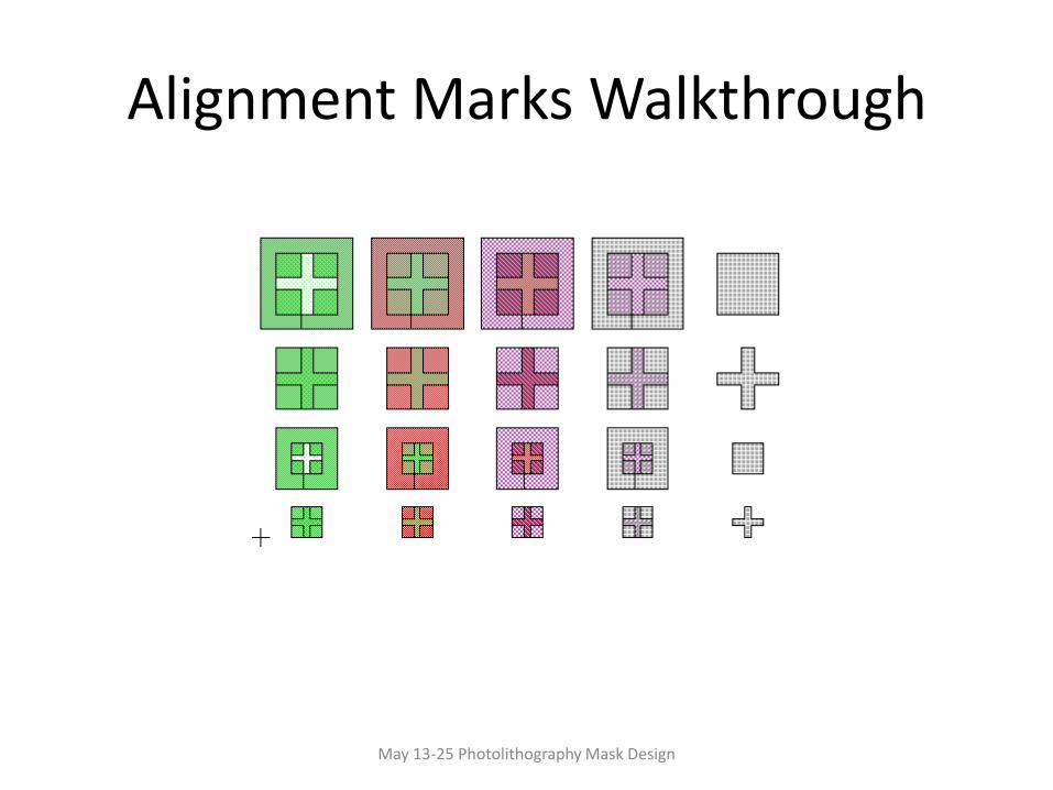
Alignment Marks Walkthrough
May 13-25 Photolithography Mask Design
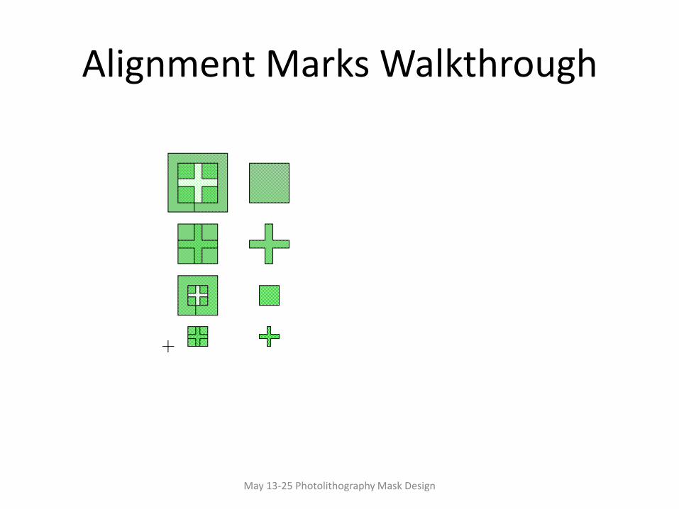
Alignment Marks Walkthrough
May 13-25 Photolithography Mask Design
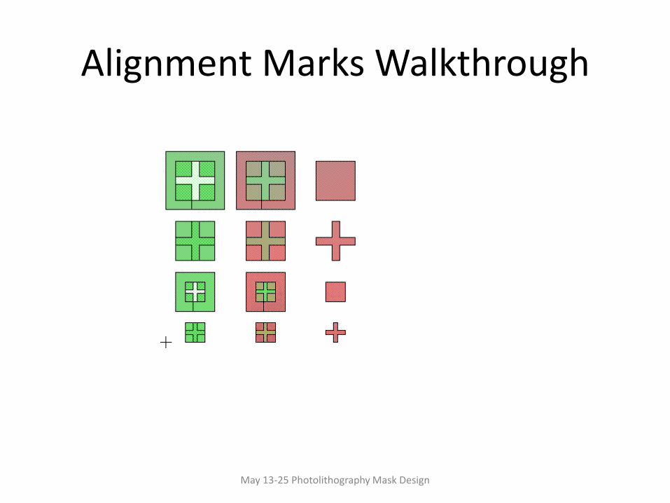
Alignment Marks Walkthrough
May 13-25 Photolithography Mask Design
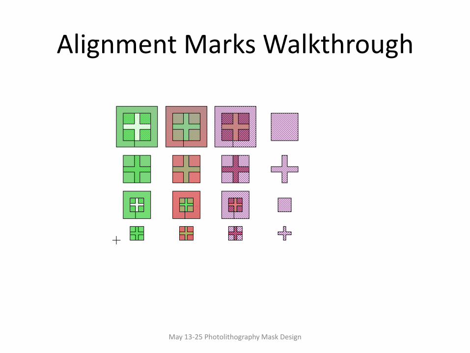
Alignment Marks Walkthrough
May 13-25 Photolithography Mask Design
Alignment Marks Walkthrough
May 13-25 Photolithography Mask Design
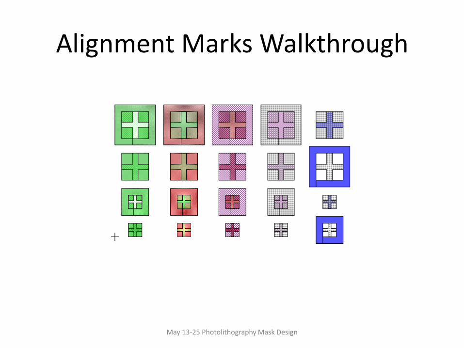
Alignment Marks Walkthrough
May 13-25 Photolithography Mask Design
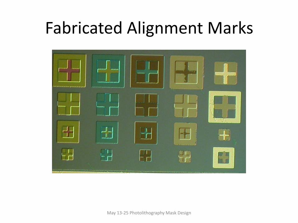
Fabricated Alignment Marks
May 13-25 Photolithography Mask Design
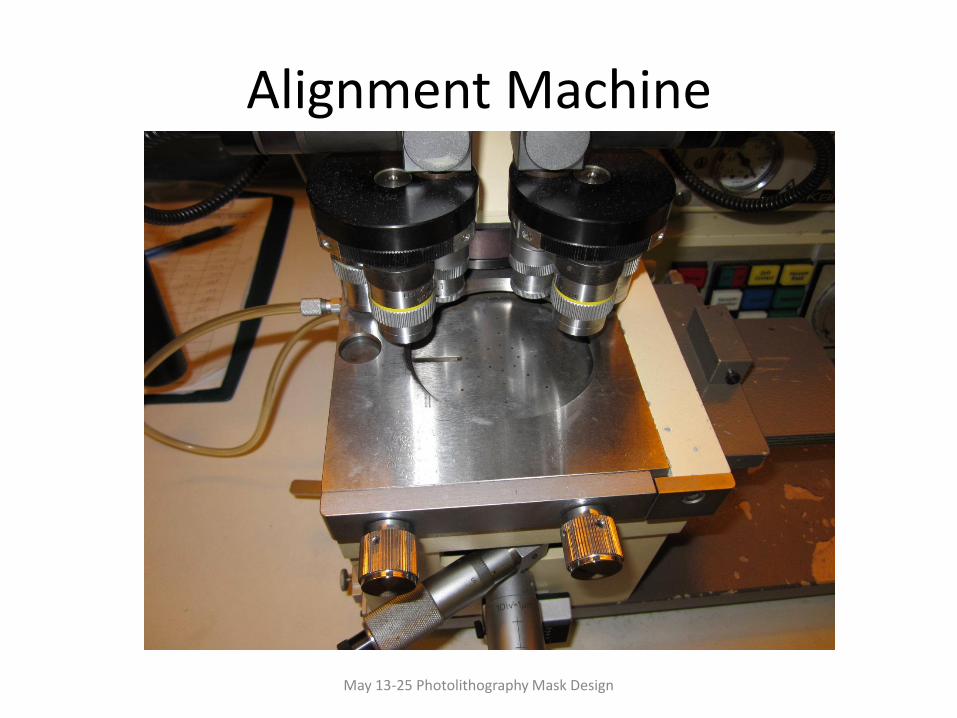
Alignment Machine
May 13-25 Photolithography Mask Design
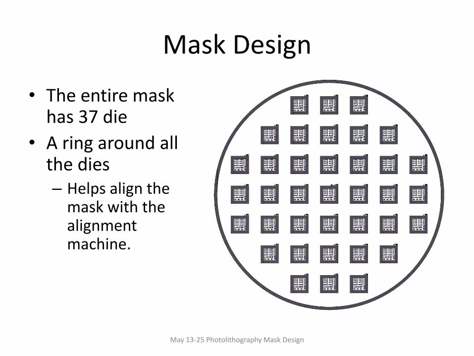
Mask Design
• The entire mask has 37 die
• A ring around all the dies – Helps align the
mask with the alignment machine.
May 13-25 Photolithography Mask Design
Challenges
• Problem: The masks cannot be tested before fabrication
• Solution: Spending extra time in the design phase working on analysis. We got each design approved by our advisor before getting any masks fabricated
May 13-25 Photolithography Mask Design
Challenges
• Problem: Developing a set of design rules for the devices
• Solution: We spent time looking at the old design, and looked for areas where they may not have left enough spacing. We met with our advisor to approve all design rules.
May 13-25 Photolithography Mask Design
Challenges
• Problem: Working with new software (L-Edit)
• Solution: Used our experience with similar software (Cadence). We spent some time going through the L-Edit documentation to better use the software features.
May 13-25 Photolithography Mask Design
Testing
• A set of wafers have been fabricated using the new mask set
– Alignment successful
– Functional transistors
– More space utilized
May 13-25 Photolithography Mask Design
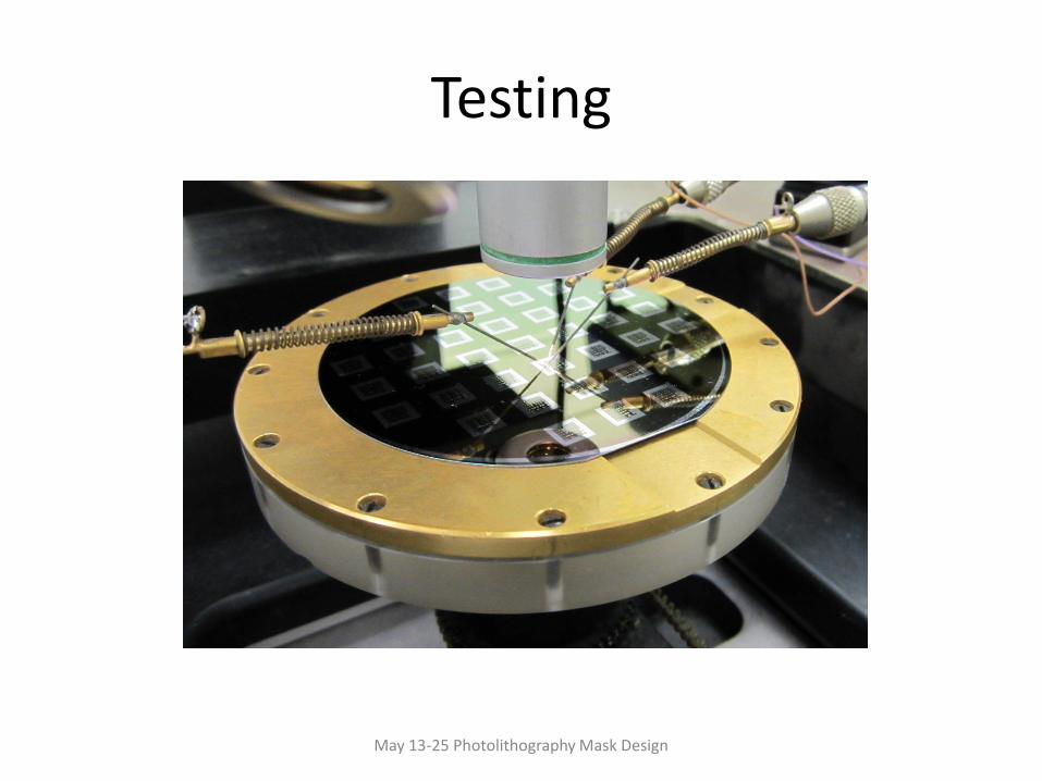
Testing
May 13-25 Photolithography Mask Design
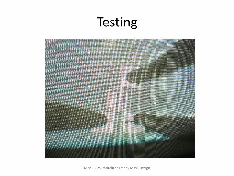
Testing
May 13-25 Photolithography Mask Design
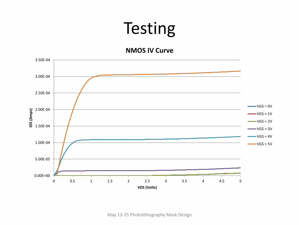
Testing
May 13-25 Photolithography Mask Design
0.00E+00
5.00E-05
1.00E-04
1.50E-04
2.00E-04
2.50E-04
3.00E-04
3.50E-04
0 0.5 1 1.5 2 2.5 3 3.5 4 4.5 5
IDS
(Am
ps)
VDS (Volts)
NMOS IV Curve
VGS = 0V
VGS = 1V
VGS = 2V
VGS = 3V
VGS = 4V
VGS = 5V
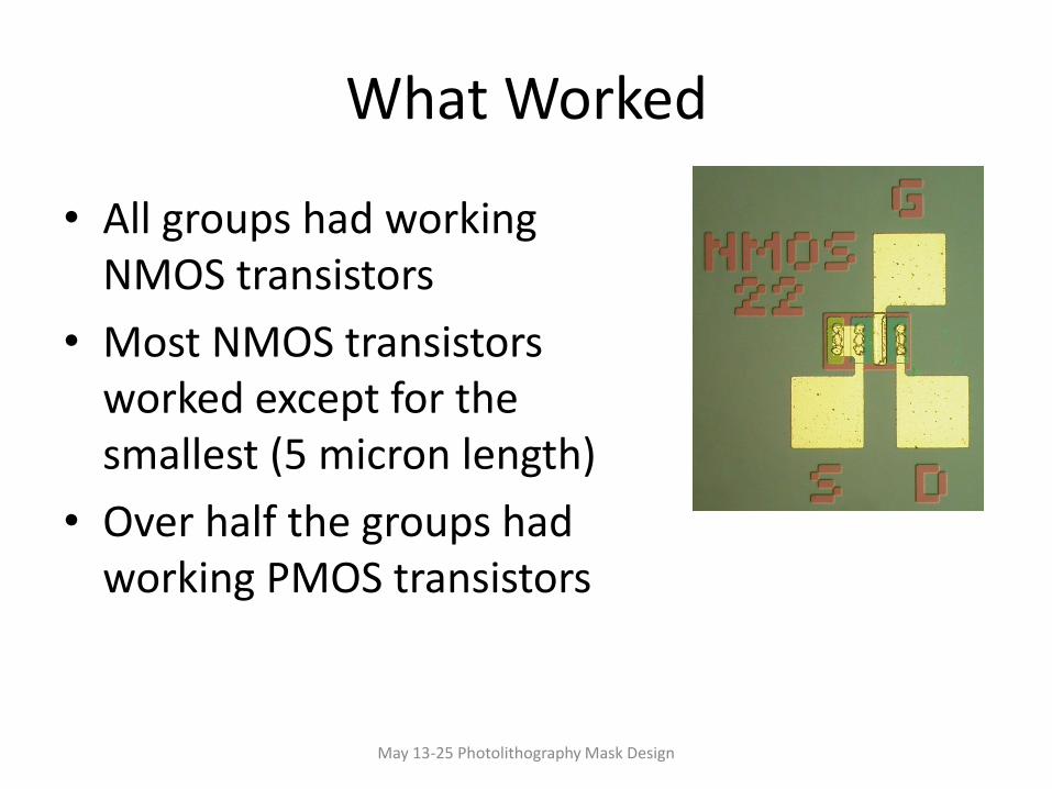
What Worked
• All groups had working NMOS transistors
• Most NMOS transistors worked except for the smallest (5 micron length)
• Over half the groups had working PMOS transistors
May 13-25 Photolithography Mask Design
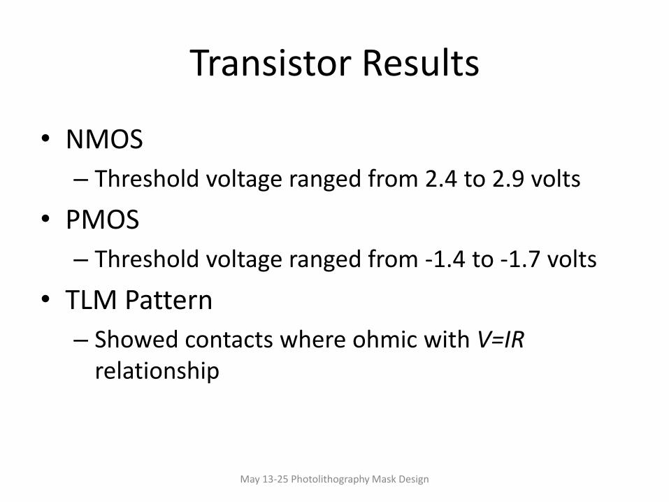
Transistor Results
• NMOS
– Threshold voltage ranged from 2.4 to 2.9 volts
• PMOS
– Threshold voltage ranged from -1.4 to -1.7 volts
• TLM Pattern
– Showed contacts where ohmic with V=IR relationship
May 13-25 Photolithography Mask Design
Questions?
May 13-25 Photolithography Mask Design