Embed Size (px)
Citation preview
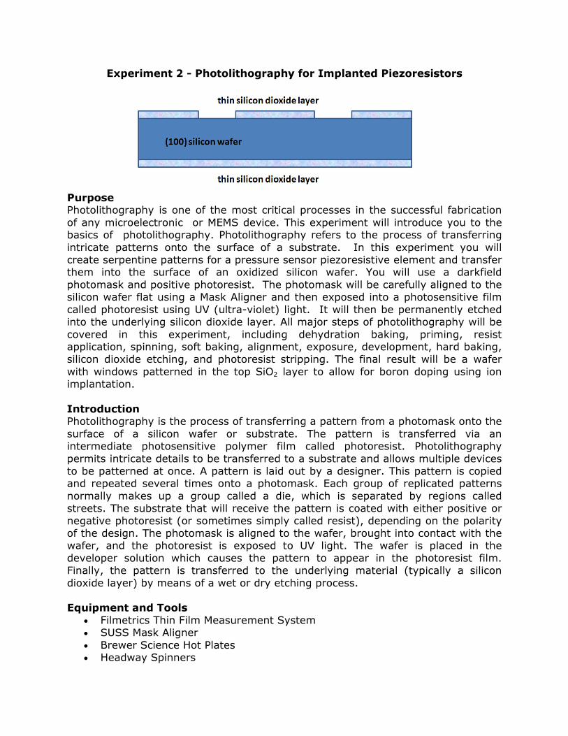
Experiment 2 - Photolithography for Implanted Piezoresistors Purpose Photolithography is one of the most critical processes in the successful fabrication of any microelectronic or MEMS device. This experiment will introduce you to the basics of photolithography. Photolithography refers to the process of transferring intricate patterns onto the surface of a substrate. In this experiment you will create serpentine patterns for a pressure sensor piezoresistive element and transfer them into the surface of an oxidized silicon wafer. You will use a darkfield photomask and positive photoresist. The photomask will be carefully aligned to the silicon wafer flat using a Mask Aligner and then exposed into a photosensitive film called photoresist using UV (ultra-violet) light. It will then be permanently etched into the underlying silicon dioxide layer. All major steps of photolithography will be covered in this experiment, including dehydration baking, priming, resist application, spinning, soft baking, alignment, exposure, development, hard baking, silicon dioxide etching, and photoresist stripping. The final result will be a wafer with windows patterned in the top SiO2 layer to allow for boron doping using ion implantation. Introduction Photolithography is the process of transferring a pattern from a photomask onto the surface of a silicon wafer or substrate. The pattern is transferred via an intermediate photosensitive polymer film called photoresist. Photolithography permits intricate details to be transferred to a substrate and allows multiple devices to be patterned at once. A pattern is laid out by a designer. This pattern is copied and repeated several times onto a photomask. Each group of replicated patterns normally makes up a group called a die, which is separated by regions called streets. The substrate that will receive the pattern is coated with either positive or negative photoresist (or sometimes simply called resist), depending on the polarity of the design. The photomask is aligned to the wafer, brought into contact with the wafer, and the photoresist is exposed to UV light. The wafer is placed in the developer solution which causes the pattern to appear in the photoresist film. Finally, the pattern is transferred to the underlying material (typically a silicon dioxide layer) by means of a wet or dry etching process. Equipment and Tools
• Filmetrics Thin Film Measurement System • SUSS Mask Aligner • Brewer Science Hot Plates • Headway Spinners
• High Power Optical Microscope • Dektak Profilometer • Wet Benches • Spin/Rinse/Dryer (SRD)
Materials and Supplies:
• Buffered Oxide Etch 6:1 (BOE 6:1) • HMDS Primer (optional) • Shipley 1813 Positive Resist • MF-319 Developer • NMP Resist Stripper
SOPs
• Filmetrics Thin Film Measurement System • Dehydration Bake using Hotplates for Shipley 1813 • Spinning for Shipley 1813 • Soft Bake for Shipley 1813 • Suss Mask Aligner • Development of Shipley 1813 • Hard Bake for Shipley 1813 • Resist Strip for Shipley 1813 • Silicon Dioxide Etch • Dektak Profiliometer
PRE_LAB ASSIGNMENT AND QUESTIONS (answer questions in your Lab Notebook and then submit a photo-copy to the TA at the start of this Lab) 1. Read the following material from Jaeger's "Introduction to Microelectronc Fabrication"
• Chapter 2 on Lithography (pages 17-42) 2. Carefully review and then print out the Standard Operating Procedures (SOPs) listed above so you have them to refer to in the cleanroom. I know there are alot! Welcome to the world of microfab!!! 3. Assuming an oxide thickness of 0.5 microns, estimate the etch time required to etch completely through the silicon dioxide layer. The Buffered Oxide Etch (BOE) BOE solution in this experiment typically etches silicon dioxide at a rate of 1200 Å/min at 22°C (room temperature). Hint: 1 micron = 10,000 Å. 4. Although we are using ion implantation for doping in the lab class, use Figure 3.10 in Jaeger to determine the minimum silicon dioxide thickness needed to provide a proper barrier layer for a boron diffusion at 1100°C for 1.5 hours. You will be taught in class how to do this for ion implantation. It is more involved than simply reading a graph.

LAB PROCEDURES (make comments and observations in your Lab Notebook) PART 1 - Oxide Measurement and Resist Application 1. Measure the thickness of your silicon dioxide film using the Filmetrics Thin Film Measurement System (see “Filmetrics” SOP). 2. Prepare the wafers for a dehydration bake. Set the hotplate temperature to 115°C. This step is necessary because it evaporates moisture from the wafer surface and promotes adhesion of the photoresist to the substrate. 3. Place the wafer on the hotplate for at least 3 minutes for dehydration bake. (see “Dehydration Bake using Hotplate for Shipley 1813” SOP for more details) 4. Remove the wafer using wafer tweezers. Be very careful because the wafer will be extremely hot. 5. Set the Headway Spinner parameters for using Shipley 1813 Positive Resist. Refer to the SOP entitled “Spinning for Shipley 1813” for details.
� SPREAD SPEED = 500 RPM for 2 seconds � SPIN SPEED = 4000 RPM for 30 seconds
6. Turn on the Spinner vacuum and carefully place the wafer on the vacuum chuck using the Headway Centering Tool. 7. (OPTIONAL) Using the designated HMDS dropper, deposit HMDS Adhesion Primer onto the wafer so that it covers the wafer by at least 50%. Close the lid and then press the START button on the spinner. Wait for the spinner to stop completely. 8. Using the appropriate Resist dropper, deposit Shipley 1813 positive resist onto the wafer, covering 50-75% of the wafer surface. This should take approximately 2 droppers full for a 100 mm (4”) wafer. Close the lid and then press the START button on the spinner. Wait for the spinner to stop completely. 9. Prepare the wafers for a Soft Bake on the Brewer Science hotplate. Set the hotplate to 115C and then place the wafer on the hotplate for 1 minute. These parameters are valid only for Shipley 1813 Positive Resist. For other resist types, please refer to the particular data sheet. This soft bake step removes solvents in the photoresist and dries the top surface of the wafer so it will not stick to the photomask during the next procedure. Refer to the “Soft Bake for Shipley 1813” SOP for additional details. The Brewer Science Hotplates are capable of 3 different types of wafer contact. We are using SOFT contact in this experiment where the wafer simply sits on the surface of the hotplate. The second mode is HARD contact where a vacuum is drawn between the wafer and hotplate. The third mode is PROXIMITY contact where the wafer floats on a thin blanket of nitrogen. You should be aware of all 3 modes for future hotplate processing.
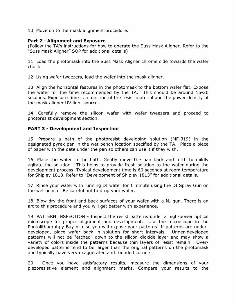
10. Move on to the mask alignment procedure. Part 2 - Alignment and Exposure (Follow the TA's instructions for how to operate the Suss Mask Aligner. Refer to the “Suss Mask Aligner” SOP for additional details) 11. Load the photomask into the Suss Mask Aligner chrome side towards the wafer chuck. 12. Using wafer tweezers, load the wafer into the mask aligner. 13. Align the horizontal features in the photomask to the bottom wafer flat. Expose the wafer for the time recommended by the TA. This should be around 15-20 seconds. Exposure time is a function of the resist material and the power density of the mask aligner UV light source. 14. Carefully remove the silicon wafer with wafer tweezers and proceed to photoresist development section. PART 3 - Development and Inspection 15. Prepare a bath of the photoresist developing solution (MF-319) in the designated pyrex pan in the wet bench location specified by the TA. Place a piece of paper with the date under the pan so others can use it if they wish. 16. Place the wafer in the bath. Gently move the pan back and forth to mildly agitate the solution. This helps to provide fresh solution to the wafer during the development process. Typical development time is 60 seconds at room temperature for Shipley 1813. Refer to “Development of Shipley 1813” for additional details. 17. Rinse your wafer with running DI water for 1 minute using the DI Spray Gun on the wet bench. Be careful not to drop your wafer. 18. Blow dry the front and back surfaces of your wafer with a N2 gun. There is an art to this procedure and you will get better with experience. 19. PATTERN INSPECTION - Inspect the resist patterns under a high-power optical microscope for proper alignment and development. Use the microscope in the Photolithograhpy Bay or else you will expose your patterns! If patterns are under-developed, place wafer back in solution for short intervals. Under-developed patterns will not be "etched" down to the silicon dioxide layer and may show a variety of colors inside the patterns because thin layers of resist remain. Over-developed patterns tend to be larger than the original patterns on the photomask and typically have very exaggerated and rounded corners. 20. Once you have satisfactory results, measure the dimensions of your piezoresistive element and alignment marks. Compare your results to the
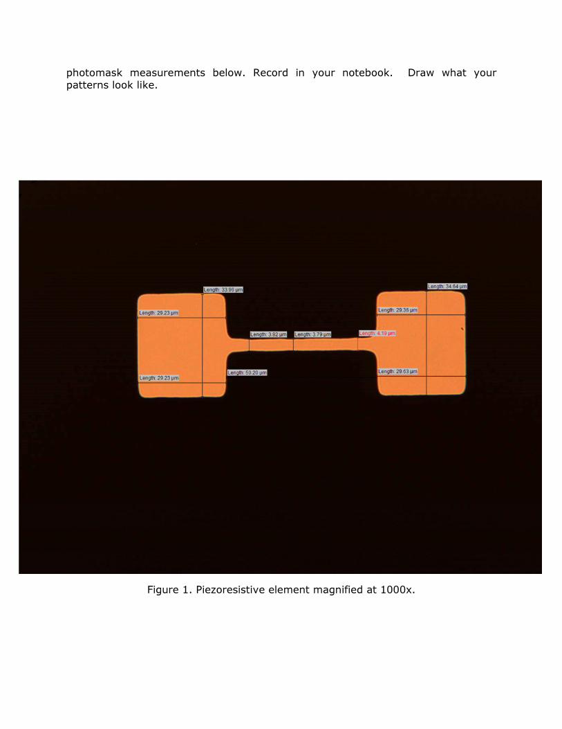
photomask measurements below. Record in your notebook. Draw what your patterns look like.
Figure 1. Piezoresistive element magnified at 1000x.
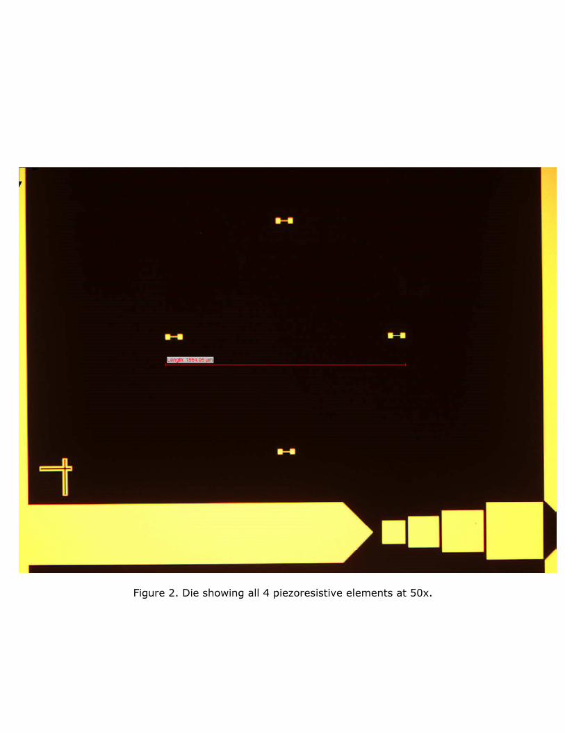
Figure 2. Die showing all 4 piezoresistive elements at 50x.
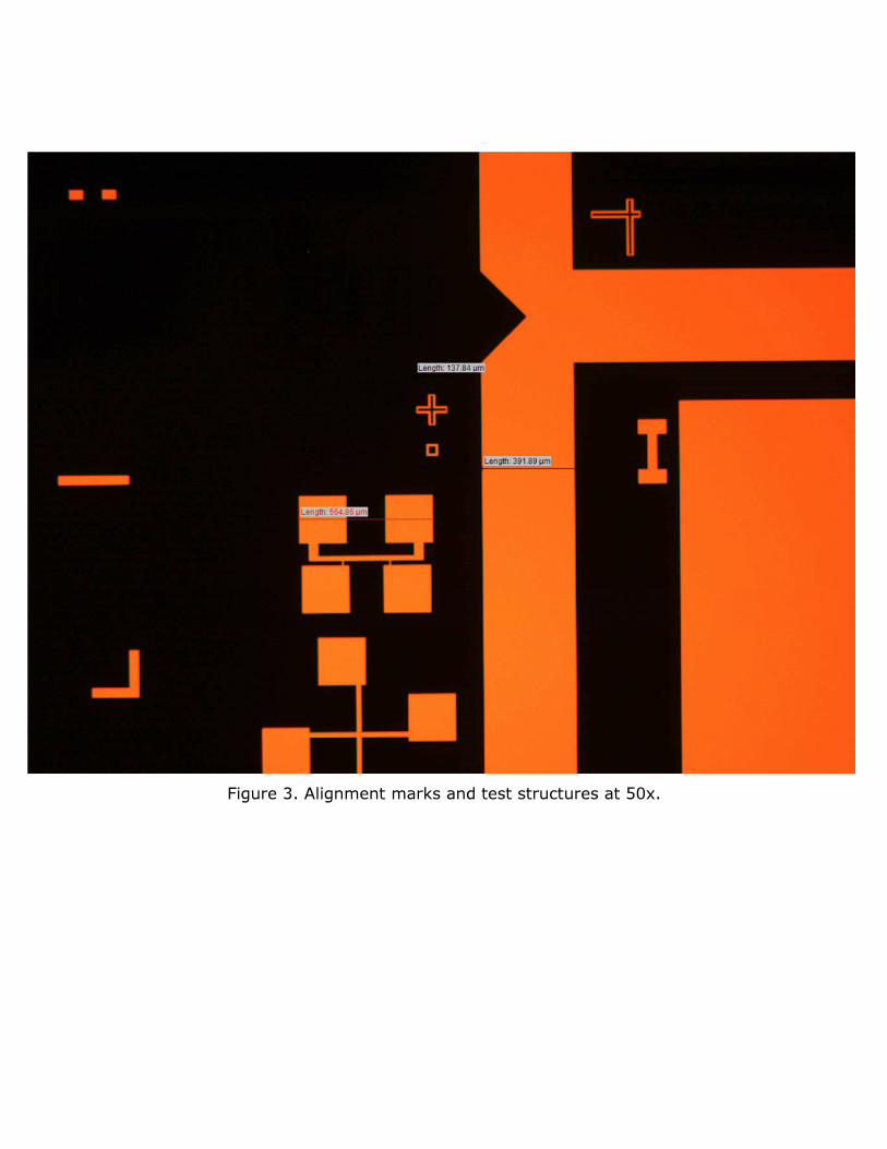
Figure 3. Alignment marks and test structures at 50x.
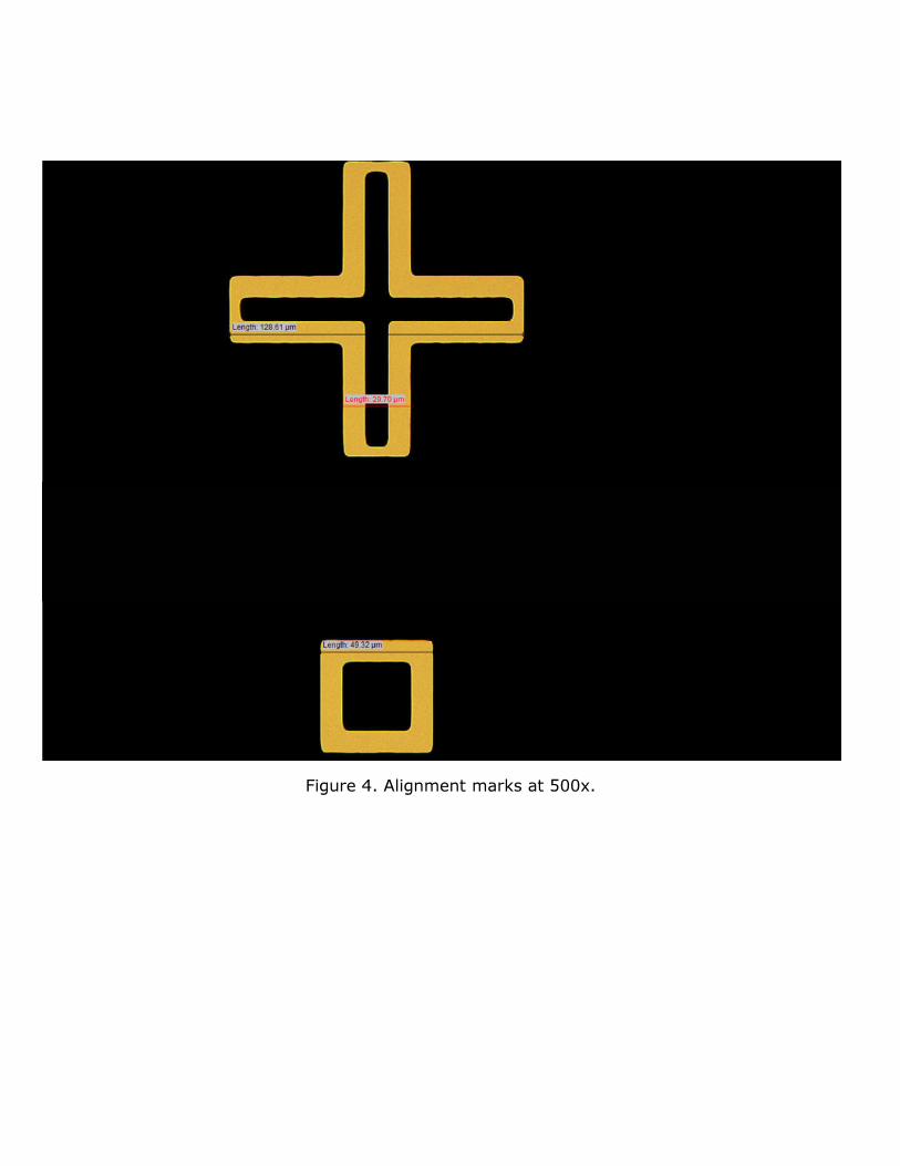
Figure 4. Alignment marks at 500x.
21. ALIGNMENT INSPECTION - Measure the distance of your patterns to the edge of the wafer flat. If properly aligned, they should be consistent across the bottom of your wafer. If your patterns are grossly misaligned to the wafer flat, you need to strip the resist, re-clean the wafers, and perform the entire photolithography step again!! PART 4 - Post Development Processing 22. Hard Bake your resist patterned wafer on the hotplate at 115C for 1 minute (see “Hardbake using Hotplate for Shipley 1813” SOP). This removes any remaining solvents and hardens the resist, thus improving its ability to function as an etch mask in Step 24. 23. Measure the thickness of your patterned photoresist using the Dektak Profilometer (see “Dektak Profilometer” SOP) OPTIONAL - Spin photoresist on the wafer backside and hardbake it to preserve the oxide during the next step. We will skip this step because we will regrow the oxide on the back of the wafer during the ion implant anneal step. 24. Transfer your patterns into the underlying silicon dioxide layer by etching your wafers in Buffered Oxide Etch (BOE). Estimate the etching time from the the data you measured in Step 1. BOE is extremely dangerous. Follow the “Silicon Dioxide Etch” SOP carefully to etch the oxide. This is a very critical step. It only takes a few minutes, but if not performed properly, it will cost you 2 days of work in the cleanroom. IMPORTANT HINT – If there is no resist on the wafer backside, you can easily tell when your oxide etching is complete by monitoring the hydrophobicity of the wafer backside. Periodically remove the cassette of wafers from the BOE to examine it (every 15 seconds or so when you get close to the target time). When BOE rushes off the wafer backside, you are done!!! 25. Rinse wafers in the Quick Dump Rinse (QDR) for several minutes and then wash them in the Spin Rinse Dryer (SRD). 26. Perform a post etch inspection using a high power optical microscope to ensure proper etching and transfer of your patterns into the oxide layer. If etched properly, you will be down to bare silicon which appears white under a high power reflected light microscope. HINT - Place a bare silicon wafer next to your sample and inspect both under the microscope for comparison. If your features are under-etched, you will observe colors inside your patterns due to oxide remaining. If over-etched, your patterns will be enlarged and rounded. If over-etching is very pronounced, you will need to start over and regrow your oxide. 27. Measure the dimensions of your piezoresistive element and alignment marks. Sketch them in your lab notebook.

28. Strip Resist using the NMP Bath in the appropriate wet bench. Immerse your wafer in NMP at room temperature for approximately 5 minutes. Then wash your wafer using the QRD and SRD. See “Resist Strip for Shipley 1813” SOP. 29. Place the wafer under the high power optical microscope and observe the patterns created during the photolithography process. 30. Measure the dimensions of one of the piezoresistive elements using the high power optical microscope. Draw a sketch in your lab notebook, including dimensions. 31. Measure the thickness of the patterned silicon dioxide layer using the profilometer (see “Dektak Profilometer” SOP). POST-LAB ASSIGNMENT AND QUESTIONS (answer questions in your Lab Notebook and then submit a photo-copy to the TA at the start of the next Lab) 1. What is the measured step height of the photoresist? How does that compare with the theoretical value from the Shipley Spin Curves? Comment. 2. What is the measured step height of the silicon dioxide using the Dektak Profilometer? How does it compare to the measurements taken with the Filmetrics system? How does it compare with the Color Chart in the Jaeger text? How does it compare with your prediction? Comment. 3. Calculate your misalignment angle to the wafer flat using your measurement in Step 21. 4. Sketch what the piezoresistve element looks like on your oxidized wafer. Include measured dimensions. Compare it to the images taken from the photomask. Evaluate the quality of your photolithographic process. How did you do? Are you a pro or novice? You will do photolithography 4 times this semester, but I’m afraid this one is critical because it defines your piezoresistive elements! 5. This experiment has dealt mainly with the photolithography process. Draw a flowchart summarizing the process with brief titles in each box.