Embed Size (px)
Citation preview
Electrochemical Microfabrication without
Photolithography – a Sustainable Manufacturing Process
S. Roy
Prof of Electrochemical Nanomaterials
School of Chemical Engineering and Advanced Materials
Institute of Nanoscale Science and Technology
University of Newcastle
Merz Court
Newcastle, NE1 7RU
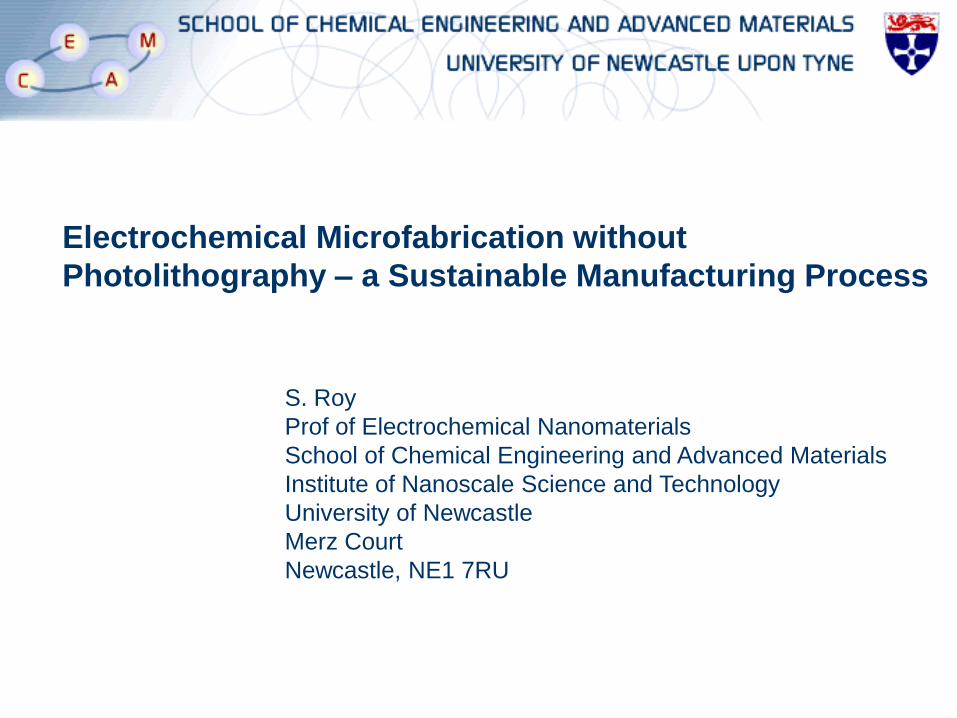
Standard Photolithographic Process
A UV- sensitive resin is used
Substrate is covered with
resin
Substrate is exposed to UV-
light
The resin is either cured or
destroyed
The resin is developed
Selected areas of substrate
are left covered with resin
Sustainability Issues
• Standard lithography techniques use a host of chemicals
(which are mainly subtractive) – Waste!
• Standard lithography is multi-step slow process – for each
design new process is developed – Slow!
• Clean rooms are expensive, require planning permissions and
licensing – impacts on SMEs – Dear!
• The issue is R-R-R (Reduce – Recycle – Reuse) : Can we
improve the sustainability of microfabricated products by RRR
• Can we stop the use of photolithography of each substrate?
• EnFACE Concept : Photolith the counter electrode!!!
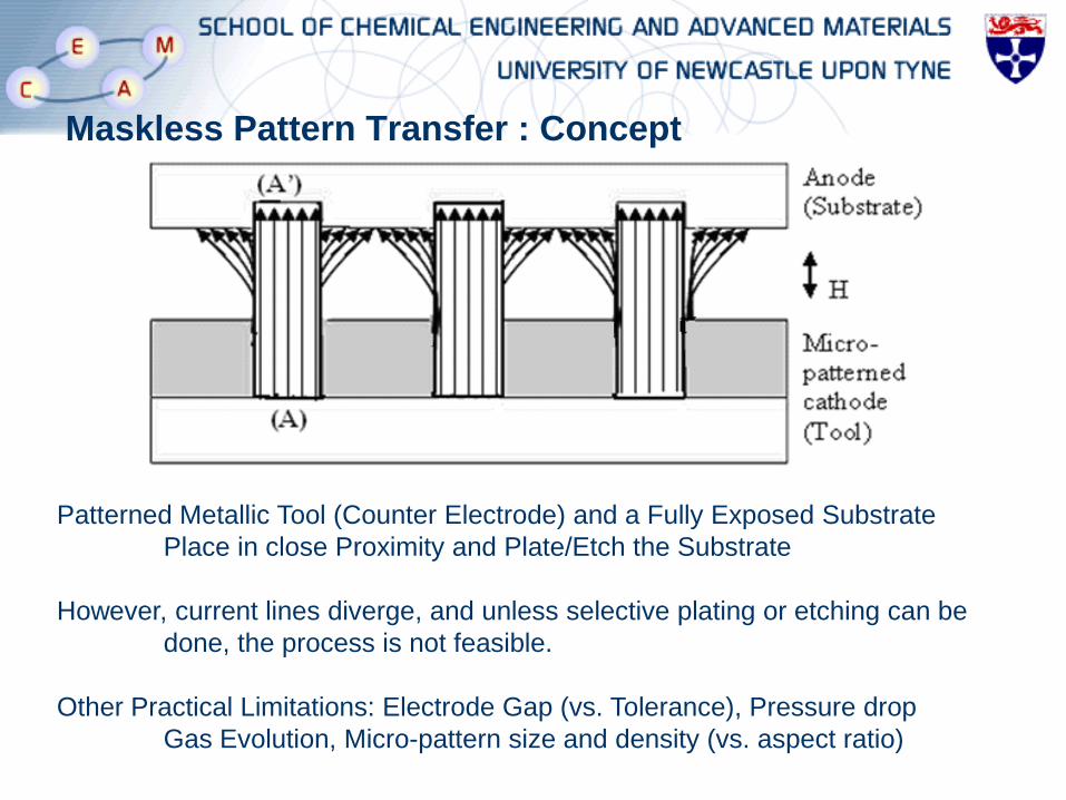
Maskless Pattern Transfer : Concept
Patterned Metallic Tool (Counter Electrode) and a Fully Exposed Substrate
Place in close Proximity and Plate/Etch the Substrate
However, current lines diverge, and unless selective plating or etching can be
done, the process is not feasible.
Other Practical Limitations: Electrode Gap (vs. Tolerance), Pressure drop
Gas Evolution, Micro-pattern size and density (vs. aspect ratio)
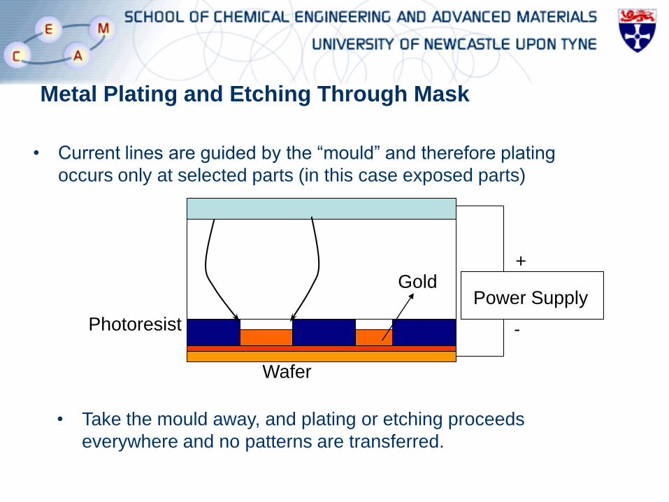
Metal Plating and Etching Through Mask
Power Supply
+
-
• Current lines are guided by the “mould” and therefore plating
occurs only at selected parts (in this case exposed parts)
Photoresist
Wafer
Gold
• Take the mould away, and plating or etching proceeds
everywhere and no patterns are transferred.
Project Development
Feasibility study
• Experimental
– Experiments to determine if selective etching and plating is attainable
– If selective plating and etching chemistry is achievable and stable
– If flow system can remove products from the electrode surface
– If plating is reproducible and stable
– Reproduced by other metals and alloys
• Modelling
– To simulate process within the system,
– Understand how pattern transfer is enabled
– Determine the important parameters for pattern transfer
Pattern Transfer on Copper Substrates
• 98.5-99% pure copper
• CuSO4 solutions which were acidified or without acid
• Etching and plating experiments
• Counter electrode was copper
• Photolithographed
• Different electrolytes were used
• Flow rates were varied
• Electrode gap was changed
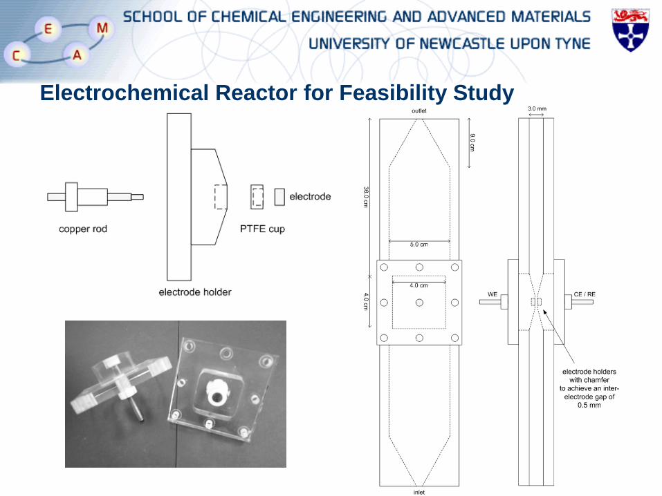
Electrochemical Reactor for Feasibility Study
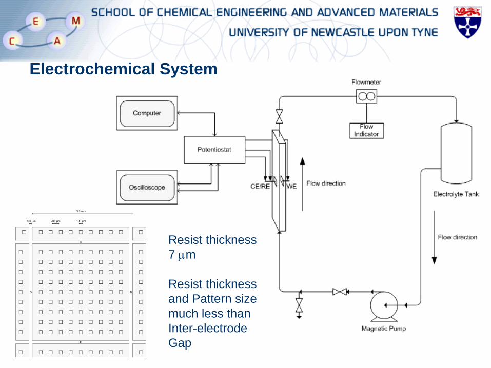
Electrochemical System
Resist thickness
7 mm
Resist thickness
and Pattern size
much less than
Inter-electrode
Gap
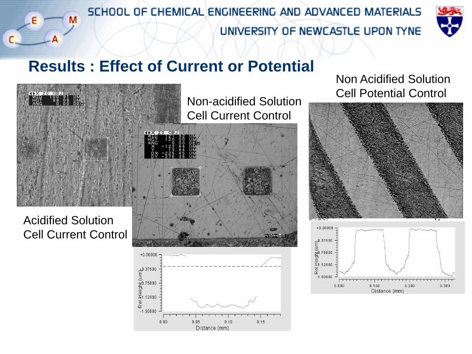
Results : Effect of Current or Potential
Acidified Solution
Cell Current Control
Non-acidified Solution
Cell Current Control
Non Acidified Solution
Cell Potential Control
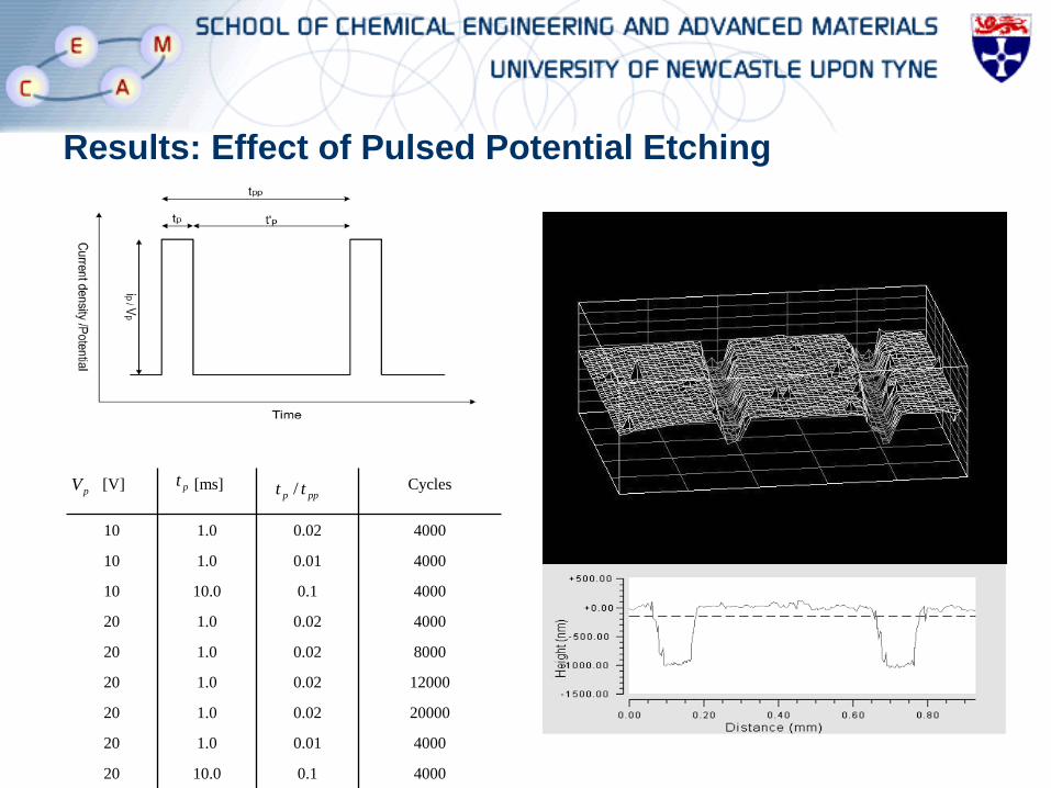
Results: Effect of Pulsed Potential Etching
pV ptppp tt /[V] [ms] Cycles
10 1.0 0.02 4000
10 1.0 0.01 4000
10 10.0 0.1 4000
20 1.0 0.02 4000
20 1.0 0.02 8000
20 1.0 0.02 12000
20 1.0 0.02 20000
20 1.0 0.01 4000
20 10.0 0.1 4000
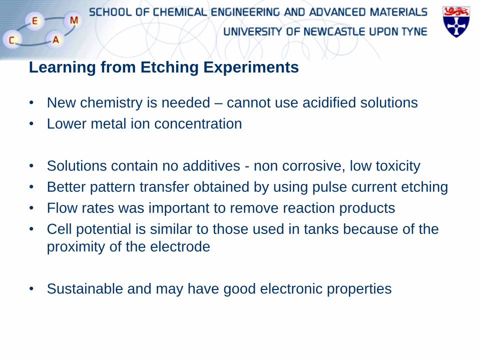
Learning from Etching Experiments
• New chemistry is needed – cannot use acidified solutions
• Lower metal ion concentration
• Solutions contain no additives - non corrosive, low toxicity
• Better pattern transfer obtained by using pulse current etching
• Flow rates was important to remove reaction products
• Cell potential is similar to those used in tanks because of the
proximity of the electrode
• Sustainable and may have good electronic properties
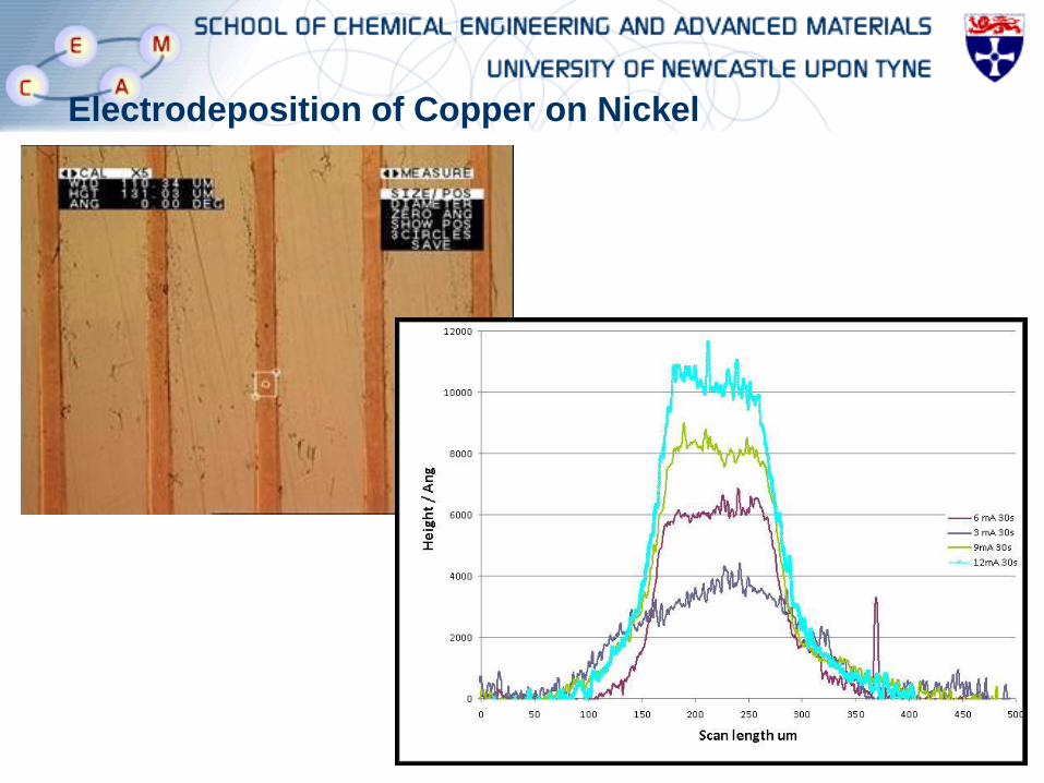
Electrodeposition of Copper on Nickel
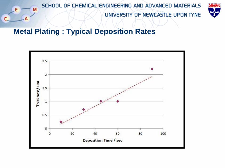
Metal Plating : Typical Deposition Rates
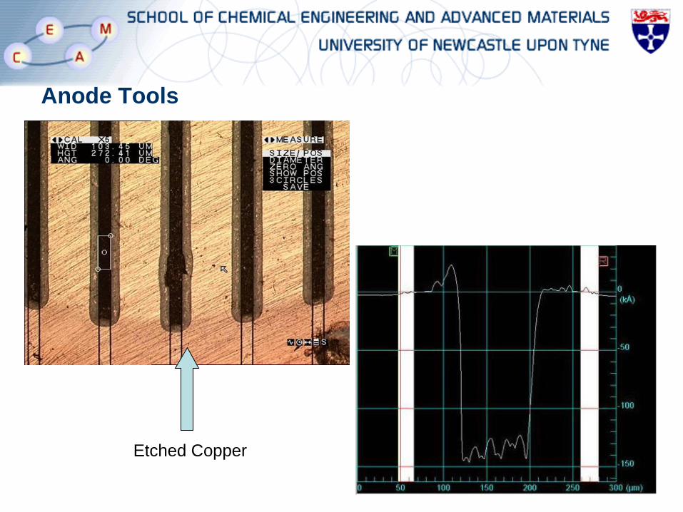
Anode Tools
Etched Copper
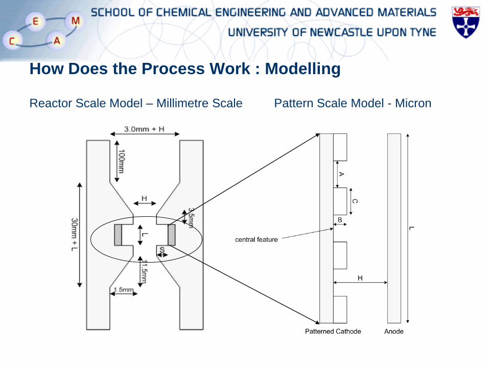
How Does the Process Work : Modelling
Reactor Scale Model – Millimetre Scale Pattern Scale Model - Micron
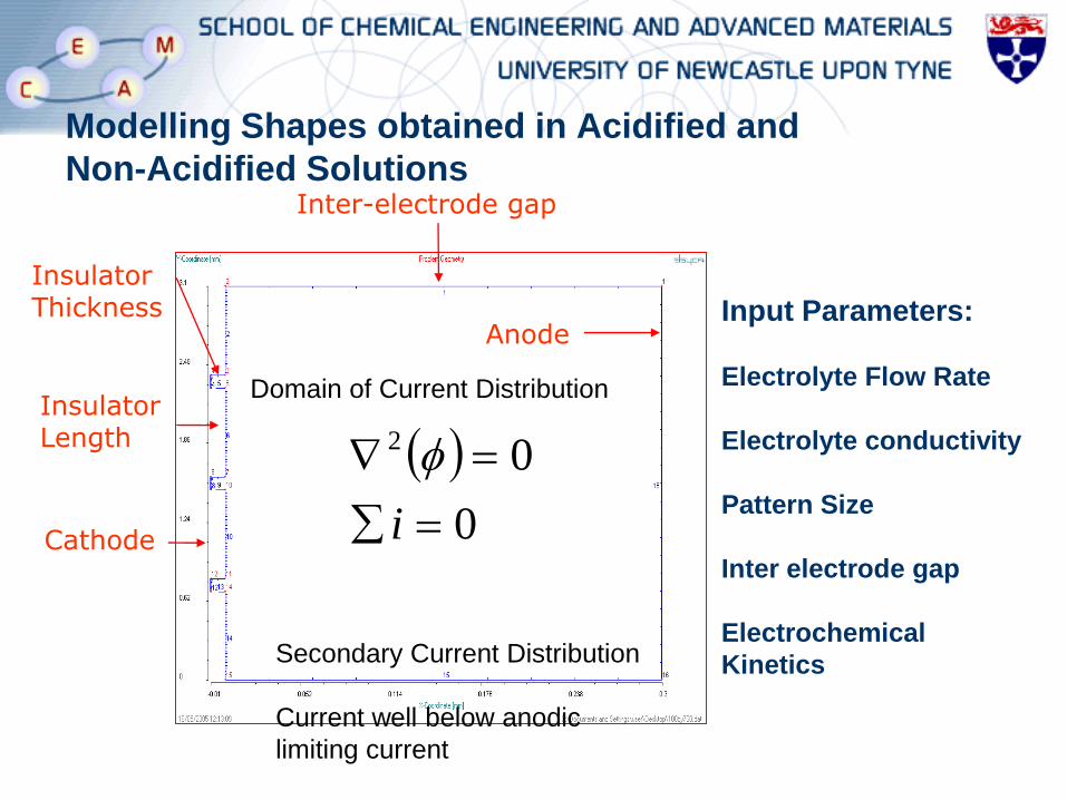
Modelling Shapes obtained in Acidified and
Non-Acidified Solutions
Input Parameters:
Electrolyte Flow Rate
Electrolyte conductivity
Pattern Size
Inter electrode gap
Electrochemical
Kinetics
Insulator Thickness
Insulator Length
Inter-electrode gap
Cathode
Anode
Domain of Current Distribution
0
02
i
Secondary Current Distribution
Current well below anodic
limiting current
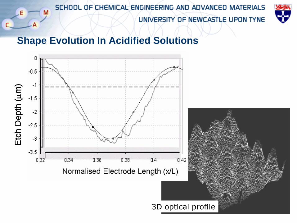
Shape Evolution In Acidified Solutions
3D optical profile
Etc
h D
epth
(m
m)
Etc
h D
epth
(m
m)
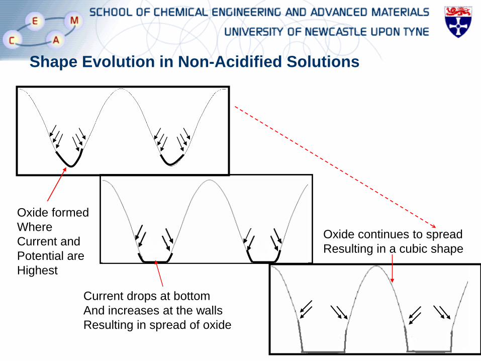
Shape Evolution in Non-Acidified Solutions
Oxide formed
Where
Current and
Potential are
Highest
Current drops at bottom
And increases at the walls
Resulting in spread of oxide
Oxide continues to spread
Resulting in a cubic shape
Potential Applications and Benefits
• EnFACE Technique can be used to transfer microscale patterns
• Reactor Technology applicable to both etching and plating
• Different metal copper, nickel and some alloys have been
structured using the technique
• Reduces the use of photolithography by 90-95%
• High cost capital equipment and chemicals unnecessary
• Low material and energy consumption
• High grade infrastructure requirement can be avoided
Publications
1. S. Roy, “A Process for Manufacturing Micro- and Nano- Devices” GB0416600.5, filed on 24th July 2004. PCT/GB2005/002795, filed 19th July 2005. Application: WO2006010888, publ. date: 2006-02-02, also published as EP1778895(A1) and EP1778895(A0). Granted in the US.
2. I. Schoenenberger and S. Roy, “An Electrochemical Method for Transferring Micro-Scale Patterns without Substrate Photolithography” Electrochim. Acta, 51, 809-819 (2005).
3. S. Roy, “Fabrication of Micro and Nano Structured Materials Using Mask-Less Processes” Invited Review Paper, J. Phys. D: Appl. Phys. 40 R413-R426 (2007).
4. S. Nouraei and S. Roy, “Analysis of Micropattern Transfer without Photolithography on Substrates”, J. Electrochem. Soc., 155(2) D97-D103 (2008).
5. S. Nouraei and S. Roy, “A Design of Experiment Approach to Electrochemical Micro- fabrication” Electrochim. Acta, 54, 2444-2449 (2009).
6. S. Roy, “EnFACE: A Mask Less Process for Circuit Fabrication” Circuit World 35(3), 8-11 (2009).
Acknowledgements
• Newcastle University Workshop
• Ivo Schönenberger
• Samane Nouraei
• Todd Green
• Qi-Bai Wu
• Tri Widayatno
• David Huntley (business advice)
• EPSRC, N-Star Equity Funding, CENAMPS
Spin Out : RoyenfaceFocused on electronics production and seeking collaboration /
partnerships.