Embed Size (px)
Citation preview
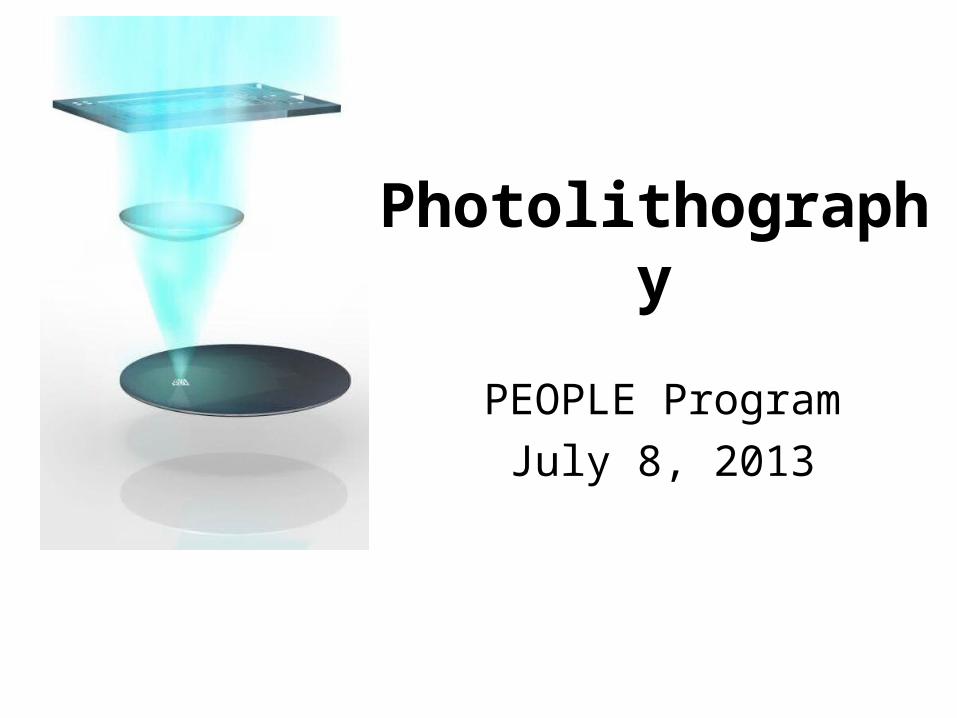
Photolithography
PEOPLE ProgramJuly 8, 2013

• Computer chips are made using photolithography
• Instead of drawing with a sharp tip, it uses light to transfer a tiny pattern from a photomask to a light-sensitive chemical
Packaging
Central Processing Unit (CPU)
How is Lithography Related to Computers?

Apple II
An early personal computer
ENIAC (Electronic Numerical Integrator and
Computer)
First general-purpose electronic computer
Apple MacBook Air
Modern laptop computer weighing
only 3 pounds!
65 years… and many advances in photolithography!
How is Lithography Related to Computers?

Photolithography• Role of the Resist:
Light exposure changes solubility and allows mask formation
• Applications: Making tiny, detailed stuff! For example, microelectronics, microfluidics, MEMS, bioanalytics, sensing, and many more
• Main Benefit: High throughput!Geissler, et al. Adv. Mater. 2004, 16, 1249-1269
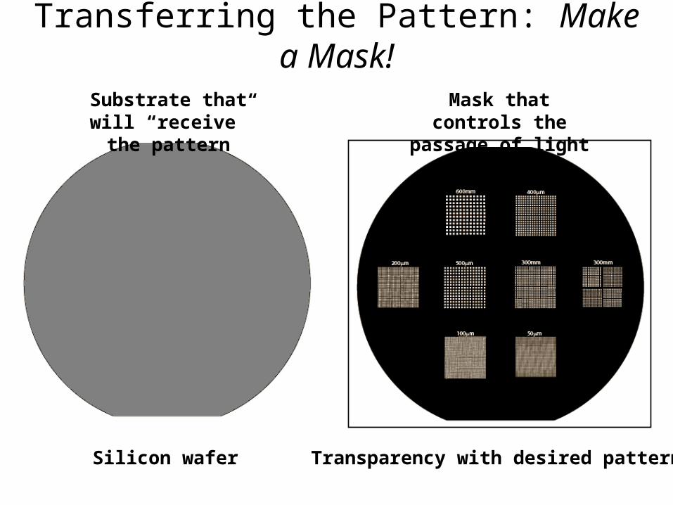
Silicon wafer Transparency with desired pattern
Transferring the Pattern: Make a Mask!
Substrate that will “receive” the pattern
Mask that controls the passage of light

Transferring the Pattern to the Silicon Wafer
Silicon WaferPhotoresist
1. Coat silicon wafer with photoresist
2. Tightly place mask on top
3. Expose to UV light
4. Develop and Rinse
Depends on the type of photoresist?
Mask
Silicon wafer
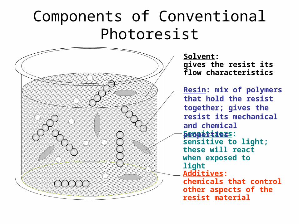
Components of Conventional Photoresist
Additives: chemicals that control other aspects of the resist material
Solvent: gives the resist its flow characteristics
Sensitizers: sensitive to light; these will react when exposed to light
Resin: mix of polymers that hold the resist together; gives the resist its mechanical and chemical properties

What it mean if something can dissolve?
What does it mean if something can’t dissolve?

What could be some What could be some examples of things that examples of things that can can
dissolve dissolve in Hin H22O?O?
What could be some What could be some examples of things that examples of things that cannot dissolve cannot dissolve in Hin H22O?O?

Our definition
*Dissolving can take other forms, as well. For example a gas can dissolve into another gas, or a gas can dissolve into a liquid.
Dissolve: A solid loses its structure and becomes dispersed into a liquid.*
Examples:•Table salt (NaCl) dissolves in water.•Sand (SiO2) does not dissolve in water.•Gasoline does not dissolve in water.•A breath-strip dissolves in your saliva.
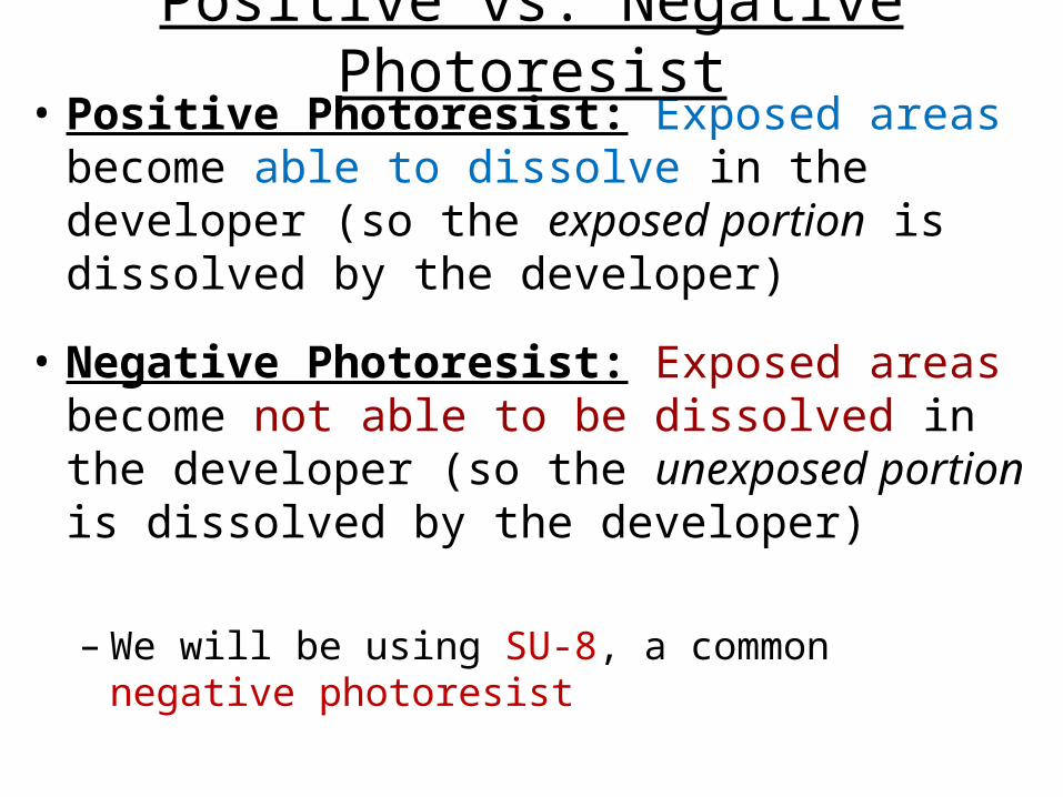
• Positive Photoresist: Exposed areas become able to dissolve in the developer (so the exposed portion is dissolved by the developer)
• Negative Photoresist: Exposed areas become not able to be dissolved in the developer (so the unexposed portion is dissolved by the developer)
– We will be using SU-8, a common negative photoresist
Positive vs. Negative Photoresist
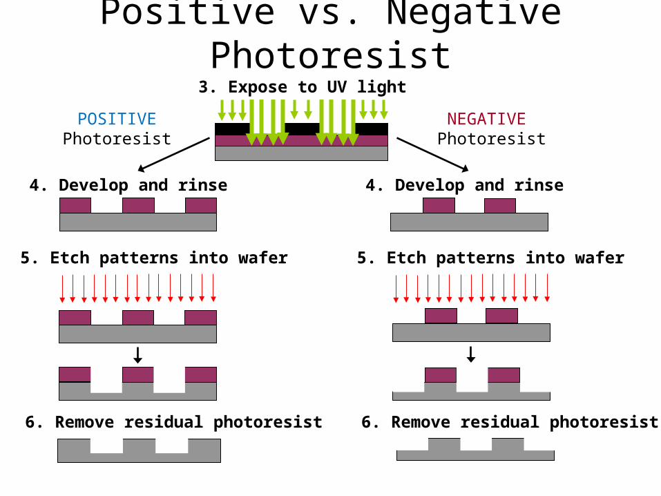
3. Expose to UV light
4. Develop and rinse 4. Develop and rinse
6. Remove residual photoresist 6. Remove residual photoresist
5. Etch patterns into wafer 5. Etch patterns into wafer
NEGATIVE Photoresist
POSITIVE Photoresist
Positive vs. Negative Photoresist

3. Expose to UV light
4. Develop and rinse 4. Develop and rinse
6. Remove residual photoresist 6. Remove residual photoresist
5. Etch patterns into wafer 5. Etch patterns into wafer
NEGATIVE Photoresist
POSITIVE Photoresist
Make sure you get it! Fill in the blanks:In a _____ photoresist, _____ light reacts with the photoresist to make it unable to be dissolved, so it is rinsed away by the _____.

A Common Photoresist: SU-8
• “Traditional” epoxy resin negative photoresist
• UV sensitized with a cationic polymerization initiator
Lee, et al. JVSTB 1995, 13, 3012-3016; Bertsch, et al. Sens. Actuators 1999, 73, 14-23; Lin, et al. J. Micromech. Microeng. 2002, 12, 590-597; Liu, et al. Adv. Mater. 2007, 19, 3783-3790
EPON® Resin SU-8 (Shell Chemical)
• Low near-UV optical absorption high aspect ratio (>15) features
Hg “I-line”, 365 nm

Review!What is cross-linking?
Do you think that a substance that has a lot of cross-links would be more easily or less easily dissolved? Why do you think so?

Negative PhotolithographyAreas exposed to light become crosslinked and don’t dissolve in the developer chemical.
Unexposed areas remain able to be dissolved by developer chemical.
Pre-exposure- photoresist
Post-exposure- photoresist
Post-develop- photoresist
UV
OxidePhotoresist
Substrate
Crosslinks
Unexposed Exposed
Soluble

• Bucky masks have been created for you
• Glass slides have been primed and coated SU-8 photoresist
• You will be performing photolithography using these masks
PEOPLE Program 2013 Your Name
Your Mask:
Today’s Activity: Photolithography

Today’s Activity: Photolithography
8) Inspect5) Post-exposure bake
6) Develop 7) Hard bake
UV Light
Mask
4) Alignment and Exposure
Resist
2) Spin coat 3) Soft bake1) Vapor prime

Step 1: Vapor Prime
The First Step of Photolithography:
• Wafer “primed” for photoresist deposition by cleaning with isopropanol and acetone
• Promotes good photoresist-to-wafer adhesion
• Followed by dehydration bake (200 °C, 5 min)
Ensures wafer surface is clean and dry
Silicon Wafer

1.Wafer secured to vacuum chuck of spin coater
2.Dispense ~3 mL of photoresist onto wafer
3.Slow spin: 500 rpm for 15 s
4.Fast spin: 6000 rpm for 60 s
• Quality measures:– time– speed– thickness– uniformity– particles and defects
Vacuum chuck
Spindle connected to spin motor
To vacuum pump
Photoresist dispenser
Step 2: Spin Coat Photoresist on Wafer
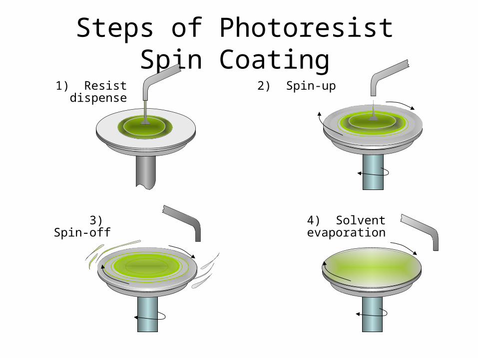
Steps of Photoresist Spin Coating
3) Spin-off 4) Solvent evaporation
1) Resist dispense 2) Spin-up
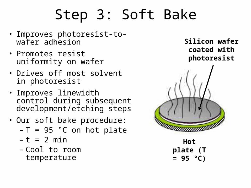
Step 3: Soft Bake• Improves photoresist-to-
wafer adhesion
• Promotes resist uniformity on wafer
• Drives off most solvent in photoresist
• Improves linewidth control during subsequent development/etching steps
• Our soft bake procedure:– T = 95 °C on hot plate– t = 2 min– Cool to room
temperature
Silicon wafer coated with photoresist
Hot plate (T = 95 °C)
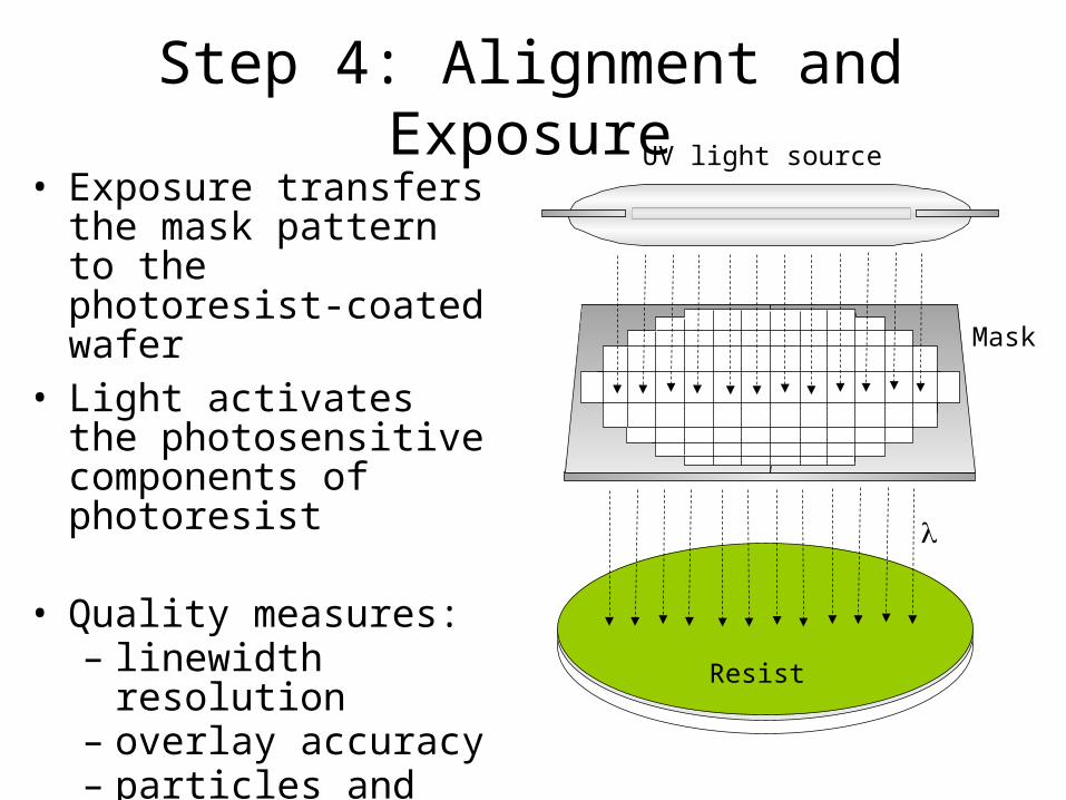
Step 4: Alignment and Exposure
• Exposure transfers the mask pattern to the photoresist-coated wafer
• Light activates the photosensitive components of photoresist
• Quality measures: – linewidth resolution– overlay accuracy– particles and
defects
UV light source
Mask
Resist

• Performed immediately after exposure
• Completes the photo reaction initiated during exposure
• Same procedure as the pre-exposure soft bake:– T = 95 °C on hot plate
– t = 2 min
– Cool to room temperature
Step 5: Post-Exposure Bake
Silicon wafer coated with exposed photoresist
Hot plate (T = 95 °C)

• Soluble areas of photoresist are dissolved by developer solvent
• Can be performed on the spin coater or simply by immersing in the developer
• Visible patterns appear on wafer: windows, islands, lines, text, images, …
• Quality measures:- line resolution- uniformity- particles and defects
Vacuum chuck
Spindle connected to spin motor
To vacuum pump
Developer dispenser
Step 6: Photoresist Development

Steps 7 and 8: Hard Bake and Inspect
• Hard bake step increases thermal, chemical, and mechanical stability of developed resist features.
• Developed resist features can be inspected (usually with magnification) to assess the quality of pattern transfer.

Summary
Silicon WaferPhotoresist
1. Coat wafer with photoresist
2. Tightly place mask on top
3. Expose to UV light
4. Develop and rinse
5. Etch patterns into wafer
6. Remove residual photoresist

Today’s Activities
Group 1
• Jake & Zahmere• Ruby & Tyrice• Roselena & Manuel• Paola & Shealyn• Terry & Mario
Group 2
• Champange & Jazmin
• Alvaro & Karen• Tashiana & Tabitha• Mariah & Zantasia• Alma & Sara

Today’s Activities
Si Wafers(Diane, Ben &
Kelly)
Photolithography
(Matt & Alfonso)
Session 1
Group 1 Group 2
Session 2
Group 2 Group 1