Embed Size (px)
Citation preview
SDP User Guide UG-502
One Technology Way • P.O. Box 9106 • Norwood, MA 02062-9106, U.S.A. • Tel: 781.329.4700 • Fax: 781.461.3113 • www.analog.com
SDP-H1 Controller Board
PLEASE SEE THE LAST PAGE FOR AN IMPORTANT WARNING AND LEGAL TERMS AND CONDITIONS. Rev. 0 | Page 1 of 32
INTRODUCTION This user guide describes the EVAL-SDP-CH1Z system demonstration platform-high speed (SDP-H1) controller board from Analog Devices, Inc. The SDP-H1 controller board is part of the Analog Devices system demonstration platform (SDP). The SDP consists of a series of controller boards, interposer boards, and daughter boards.
SDP controller boards provide a means of communicating with the PC from the system under evaluation. Interposer boards route signals between two connectors. Daughter boards are a collection of product evaluation boards and Circuits From The Lab™ (CFTL) reference circuit boards. The SDP-H1 is used as part of the evaluation system for many Analog Devices compo-nents and reference circuits. The primary audience for this user guide is a system engineer who seeks to understand how to set up the SDP-H1 board and begin USB communications to the PC.
The SDP-H1 board is designed to be used in conjunction with various Analog Devices component evaluation boards and Circuits From The Lab reference circuits as part of a customer evaluation environment. The SDP-H1 provides USB connectiv-ity through a USB 2.0 high speed connection to the computer allowing users to evaluate components on this platform from a PC application. The SDP-H1 has a Xilinx Spartan-6 FPGA and an ADSP-BF527 Blackfin processor. The Xilinx Spartan-6 FPGA connects to an FMC low pin count (LPC) connector. This connector provides power to the daughter board (see the Power section for more details) and LVDS and LVCMOS signal support. The Blackfin processor peripherals communication lines are available through an SDP 120-pin small footprint connectors. The Blackfin processor also provides the USB controller for the board and allows the user to configure the FPGA.
The SDP-H1 user guide provides instructions for installing the SDP-H1 hardware (EVAL-SDP-CH1Z board) and software onto your computer. The necessary installation files are provided with the evaluation daughter board package. The Getting Started section provides software and hardware installation procedures, PC system requirements, and basic board informa-tion. The Hardware Description section provides information on the EVAL-SDP-CH1Z components. The EVAL-SDP-CH1Z schematics are provided in the Schematics section.
UG-502 SDP User Guide
Rev. 0 | Page 2 of 32
TABLE OF CONTENTS Introduction ...................................................................................... 1 Revision History ............................................................................... 2 Product Overview ............................................................................. 3
Technical or Customer Support.................................................. 3 Product Information .................................................................... 3 Regulatory Compliance ............................................................... 3
Getting Started .................................................................................. 4 Package Contents .......................................................................... 4 PC Configuration ......................................................................... 4 USB Installation ............................................................................ 4
Powering Up/Powering Down the SDP .....................................4 Hardware Description.......................................................................5
LEDs ................................................................................................5 SDP Connector Details .................................................................5 FMC Connector Details ............................................................ 10 SMA Connectors ........................................................................ 15 Power............................................................................................ 15 Mechanical Specifications ......................................................... 15
Schematics ....................................................................................... 17
REVISION HISTORY 4/13—Revision 0: Initial Version
SDP User Guide UG-502
Rev. 0 | Page 3 of 32
PRODUCT OVERVIEW The SDP-H1 board features
• Xilinx Spartan-6 FPGA • DDR2
• Micron MT47H32M16HR-25E:G – 8Mb × 16 bits × 4 Banks (512 Mb/64 MB)
• SRAM • ISSI IS61WV25616BLL-10BLI – 256Kb × 16 bits
(4 Mb/512 Kb) • 1 × 160-pin FMC-LPC connector. (For further infor-
mation, see the VITA 57 specification FMC Marketing Alliance available from VITA Technologies.) • Samtec ASP-134603-01 • Up to 1,080 Mb/s LVDS • Single-ended LVCMOS • Power
• Analog Devices ADSP-BF527 Blackfin processor • Core performance up to 600 MHz • 208-ball CSP-BGA package • 5 Mb of internal RAM memory
• 24 MHz CLKIN oscillator • 32 Mb flash memory
• Numonyx M25P32 • SDRAM memory
• Micron MT48LC16M16A2P-6A − 16 Mb × 16 bits (256 Mb/32 MB)
• 1 × 120-pin small foot print connectors • Hirose FX8-120P-SV1(91), 120-pin header
• 4 × footprints for SMA connectors • 1 × pair of footprints for external differential clock • 1 × pair of footprints for external differential trigger
• Blackfin processor peripherals exposed • SPI • SPORT • TWI/I2C • GPIO • PPI • Asynchronous parallel • Timers
For more information, go to http://www.analog.com/sdp.
TECHNICAL OR CUSTOMER SUPPORT You can reach Analog Devices customer support in the following ways:
• Visit the SDP website at http://www.analog.com/sdp
• Email processor questions to • [email protected] (worldwide support) • [email protected] (Europe support) • [email protected] (China support)
• Phone questions to 1-800-ANALOGD
• Contact your Analog Devices local sales office or authorized distributor.
• Send questions by mail to Analog Devices, Inc. Three Technology Way P.O. Box 9106 Norwood, MA 02062-9106 USA
PRODUCT INFORMATION Product information can be obtained from the Analog Devices website.
Analog Devices Website
The Analog Devices website, www.analog.com, provides information about a broad range of products—analog integrated circuits, amplifiers, converters, and digital signal processors.
Note that MyAnalog.com is a free feature of the Analog Devices website that allows customization of a web page to display only the latest information about products of interest to you. You can choose to receive weekly email notifications containing updates to the web pages that meet your interests, including documenta-tion errata against all documents. MyAnalog.com provides access to books, application notes, data sheets, code examples, and more.
Visit MyAnalog.com to sign up. If you are a registered user, just log on. Your user name is your email address.
REGULATORY COMPLIANCE The EVAL-SDP-CH1Z is designed to be used solely in a labora-tory environment. The board is not intended for use as a consumer end product or as a portion of a consumer end product. The board is an open system design, which does not include a shielded enclosure and therefore may cause interfer-ence to other electrical devices in close proximity. This board should not be used in or near any medical equipment or RF devices. Store unused boards in the protective shipping package.
UG-502 SDP User Guide
Rev. 0 | Page 4 of 32
GETTING STARTED This section provides specific information to assist you with using the SDP-H1 board as part of your evaluation system.
The following topics are covered:
• Package contents • PC configuration • USB installation • Powering up/powering down the SDP
PACKAGE CONTENTS Your EVAL-SDP-CH1Z board package contains the following:
• EVAL-SDP-CH1Z board • 1 m USB Standard-A to Mini-B cable • 12 V 30 W wall wart
Contact the vendor where you purchased your SDP-H1 board or contact Analog Devices if anything is missing.
PC CONFIGURATION For correct operation of the SDP board, your computer must have the following minimum configuration:
• Windows® XP Service Pack 2 -32 bit, Windows Vista 32-bit/64-bit, or Windows 7 32-bit/64-bit
• USB 2.0 port
When removing the SDP-H1 board from the package, handle the board carefully to avoid the discharge of static electricity, which can damage some components.
USB INSTALLATION Perform the following tasks to safely install the SDP-H1 board onto the computer. There are two stages in the soft- ware application installation procedure. The first stage installs the application software. The second stage installs the .NET Framework 3.5 and the necessary drivers.
Installing the Software
1. Run the application install provided. The first stage installs the applications GUI and the necessary support files onto the computer.
2. Immediately following the application install, the .NET Framework 3.5 and the driver package for the SDP board is installed. If the .NET Framework 3.5 is already preinstalled on the computer in question, this stage is skipped and Step 2 will consist of a driver package installation only.
Connecting the SDP-H1 Board to the PC
Attach the SDP-H1 board to a USB 2.0 port on the computer via the Standard-A to Mini-B cable provided. The SDP-H1 must be powered using the enclosed wall-wart power supply.
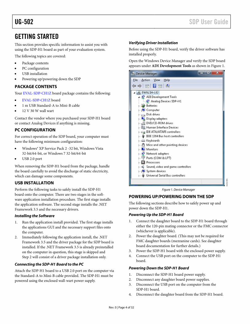
Verifying Driver Installation
Before using the SDP-H1 board, verify the driver software has installed properly.
Open the Windows Device Manager and verify the SDP board appears under ADI Development Tools as shown in Figure 1.
Figure 1. Device Manager
POWERING UP/POWERING DOWN THE SDP The following sections describe how to safely power up and power down the SDP-H1.
Powering Up the SDP-H1 Board
1. Connect the daughter board to the SDP-H1 board through either the 120-pin mating connector or the FMC connector (whichever is applicable).
2. Power the daughter board. (This may not be required for FMC daughter boards (mezzanine cards). See daughter board documentation for further details.)
3. Power the SDP-H1 board with the enclosed power supply. 4. Connect the USB port on the computer to the SDP-H1
board.
Powering Down the SDP-H1 Board
1. Disconnect the SDP-H1 board power supply. 2. Disconnect any daughter board power supplies. 3. Disconnect the USB port on the computer from the
SDP-H1 board. 4. Disconnect the daughter board from the SDP-H1 board.
1121
2-00
1
SDP User Guide UG-502
Rev. 0 | Page 5 of 32
HARDWARE DESCRIPTION This section describes the hardware design of the EVAL-SDP-CH1Z board.
The following topics are covered:
LEDs—This section describes the SDP on-board LEDs. Connector Details—This section details the pin
assignments on the FMC connector and the 120-pin connector. The SMA connectors are also covered.
Power—This section lists power requirements of the SDP and identifies connector power inputs and output pins.
Mechanical specifications—This section provides dimensional information.
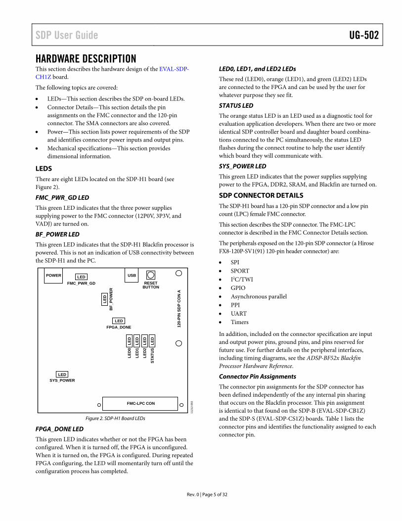
LEDS There are eight LEDs located on the SDP-H1 board (see Figure 2).
FMC_PWR_GD LED
This green LED indicates that the three power supplies supplying power to the FMC connector (12P0V, 3P3V, and VADJ) are turned on.
BF_POWER LED
This green LED indicates that the SDP-H1 Blackfin processor is powered. This is not an indication of USB connectivity between the SDP-H1 and the PC.
Figure 2. SDP-H1 Board LEDs
FPGA_DONE LED
This green LED indicates whether or not the FPGA has been configured. When it is turned off, the FPGA is unconfigured. When it is turned on, the FPGA is configured. During repeated FPGA configuring, the LED will momentarily turn off until the configuration process has completed.
LED0, LED1, and LED2 LEDs
These red (LED0), orange (LED1), and green (LED2) LEDs are connected to the FPGA and can be used by the user for whatever purpose they see fit.
STATUS LED
The orange status LED is an LED used as a diagnostic tool for evaluation application developers. When there are two or more identical SDP controller board and daughter board combina-tions connected to the PC simultaneously, the status LED flashes during the connect routine to help the user identify which board they will communicate with.
SYS_POWER LED
This green LED indicates that the power supplies supplying power to the FPGA, DDR2, SRAM, and Blackfin are turned on.
SDP CONNECTOR DETAILS The SDP-H1 board has a 120-pin SDP connector and a low pin count (LPC) female FMC connector.
This section describes the SDP connector. The FMC-LPC connector is described in the FMC Connector Details section.
The peripherals exposed on the 120-pin SDP connector (a Hirose FX8-120P-SV1(91) 120-pin header connector) are:
SPI SPORT I2C/TWI GPIO Asynchronous parallel PPI UART Timers
In addition, included on the connector specification are input and output power pins, ground pins, and pins reserved for future use. For further details on the peripheral interfaces, including timing diagrams, see the ADSP-BF52x Blackfin Processor Hardware Reference.
Connector Pin Assignments
The connector pin assignments for the SDP connector has been defined independently of the any internal pin sharing that occurs on the Blackfin processor. This pin assignment is identical to that found on the SDP-B (EVAL-SDP-CB1Z) and the SDP-S (EVAL-SDP-CS1Z) boards. Table 1 lists the connector pins and identifies the functionality assigned to each connector pin.
POWER USB
RESETBUTTON
120-
PIN
SD
P C
ON
A
LEDFMC_PWR_GD
LEDFPGA_DONE
FMC-LPC CON
SYS_POWER
LED
LED
LED
LED
LED
LED
LED
0
LED
1
LED
2
STAT
US
BF_
POW
ER
1121
2-00
2
UG-502 SDP User Guide
Rev. 0 | Page 6 of 32
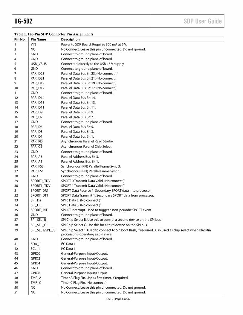
Table 1. 120-Pin SDP Connector Pin Assignments Pin No. Pin Name Description 1 VIN Power to SDP Board. Requires 300 mA at 5 V. 2 NC No Connect. Leave this pin unconnected. Do not ground. 3 GND Connect to ground plane of board. 4 GND Connect to ground plane of board. 5 USB_VBUS Connected directly to the USB +5 V supply. 6 GND Connect to ground plane of board. 7 PAR_D23 Parallel Data Bus Bit 23. (No connect.)1 8 PAR_D21 Parallel Data Bus Bit 21. (No connect.)1 9 PAR_D19 Parallel Data Bus Bit 19. (No connect.)1 10 PAR_D17 Parallel Data Bus Bit 17. (No connect.)1 11 GND Connect to ground plane of board. 12 PAR_D14 Parallel Data Bus Bit 14. 13 PAR_D13 Parallel Data Bus Bit 13. 14 PAR_D11 Parallel Data Bus Bit 11. 15 PAR_D9 Parallel Data Bus Bit 9. 16 PAR_D7 Parallel Data Bus Bit 7. 17 GND Connect to ground plane of board. 18 PAR_D5 Parallel Data Bus Bit 5. 19 PAR_D3 Parallel Data Bus Bit 3. 20 PAR_D1 Parallel Data Bus Bit 1. 21 PAR_RD Asynchronous Parallel Read Strobe.
22 PAR_CS Asynchronous Parallel Chip Select.
23 GND Connect to ground plane of board. 24 PAR_A3 Parallel Address Bus Bit 3. 25 PAR_A1 Parallel Address Bus Bit 1. 26 PAR_FS3 Synchronous (PPI) Parallel Frame Sync 3. 27 PAR_FS1 Synchronous (PPI) Parallel Frame Sync 1. 28 GND Connect to ground plane of board. 29 SPORT0_TDV SPORT 0 Transmit Data Valid. (No connect.)1 30 SPORT1_TDV SPORT 1 Transmit Data Valid. (No connect.)1 31 SPORT_DR1 SPORT Data Receive 1. Secondary SPORT data into processor. 32 SPORT_DT1 SPORT Data Transmit 1. Secondary SPORT data from processor. 33 SPI_D2 SPI 0 Data 2. (No connect.)1 34 SPI_D3 SPI 0 Data 3. (No connect.)1 35 SPORT_INT SPORT Interrupt. Used to trigger a non-periodic SPORT event. 36 GND Connect to ground plane of board. 37 SPI_SEL_B SPI Chip Select B. Use this to control a second device on the SPI bus.
38 SPI_SEL_C SPI Chip Select C. Use this for a third device on the SPI bus.
39 SPI_SEL1/SPI_SS SPI Chip Select 1. Used to connect to SPI boot flash, if required. Also used as chip select when Blackfin processor is operating as SPI slave.
40 GND Connect to ground plane of board. 41 SDA_1 I2C Data 1. 42 SCL_1 I2C Data 1. 43 GPIO0 General-Purpose Input/Output. 44 GPIO2 General-Purpose Input/Output. 45 GPIO4 General-Purpose Input/Output. 46 GND Connect to ground plane of board. 47 GPIO6 General-Purpose Input/Output. 48 TMR_A Timer A Flag Pin. Use as first timer, if required. 49 TMR_C Timer C Flag Pin. (No connect.)1 50 NC No Connect. Leave this pin unconnected. Do not ground. 51 NC No Connect. Leave this pin unconnected. Do not ground.
SDP User Guide UG-502
Rev. 0 | Page 7 of 32
Pin No. Pin Name Description 52 GND Connect to ground plane of board. 53 NC No Connect. Leave this pin unconnected. Do not ground. 54 NC No Connect. Leave this pin unconnected. Do not ground. 55 NC No Connect. Leave this pin unconnected. Do not ground. 56 EEPROM_A0 EEPROM A0. Connect to A0 address line of the EEPROM. 57 RESET_OUT Active low reset signal from processor board.
58 GND Connect to ground plane of board. 59 UART_RX UART Receive Data. 60 RESET_IN Active low pin to reset controller board.
61 BMODE1 Boot Mode 1. Pull up with 10 kΩ resistor to set SDP to boot from SPI Flash. Enabled on Connector A only. 62 UART_TX UART Transmit Data. 63 GND Connect to ground plane of board. 64 SLEEP Active low sleep from processor board.
65 WAKE External wake up to processor board. 66 NC No Connect. Leave this pin unconnected. Do not ground. 67 NC No Connect. Leave this pin unconnected. Do not ground. 68 NC No Connect. Leave this pin unconnected. Do not ground. 69 GND Connect to ground plane of board. 70 NC No Connect. Leave this pin unconnected. Do not ground. 71 CLK_OUT CLK_OUT from processor. 72 TMR_D Timer D Flag Pin. 73 TMR_B Timer B Flag Pin. Use as second timer, if required. 74 GPIO7 General-Purpose Input/Output. 75 GND Connect to ground plane of board. 76 GPIO5 General-Purpose Input/Output. 77 GPIO3 General-Purpose Input/Output. 78 GPIO1 General-Purpose Input/Output. 79 SCL_0 I2C Clock 0. Daughter board EEPROM must be connected to this bus. 80 SDA_0 I2C Data 0. Daughter board EEPROM must be connected to this bus. 81 GND Connect to ground plane of board. 82 SPI_CLK SPI Clock. 83 SPI_MISO SPI Master In, Slave Out Data. 84 SPI_MOSI SPI Master Out, Slave In Data. 85 SPI_SEL_A SPI Chip Select A. Use this to control the first device on the SPI bus.
86 GND Connect to ground plane of board. 87 SPORT_TSCLK SPORT Transmit Clock. 88 SPORT_DT0 SPORT Data Transmit 0. Primary SPORT data from processor. 89 SPORT_TFS SPORT Transmit Frame Sync. 90 SPORT_RFS SPORT Receive Frame Sync. 91 SPORT_DR0 SPORT Data Receive 0. Primary SPORT data into processor. 92 SPORT_RSCLK SPORT Receive Clock. 93 GND Connect to ground plane of board. 94 PAR_CLK Clock for Synchronous Parallel Interface (PPI). 95 PAR_FS2 Synchronous (PPI) Parallel Frame Sync 2. 96 PAR_A0 Parallel Address Bus Bit 0. 97 PAR_A2 Parallel Address Bus Bit 2. 98 GND Connect to ground plane of board. 99 PAR_INT Parallel Interrupt. Used to trigger a nonperiodic parallel event. 100 PAR_WR Asynchronous Parallel Write Strobe.
101 PAR_D0 Parallel Data Bus Bit 0. 102 PAR_D2 Parallel Data Bus Bit 2. 103 PAR_D4 Parallel Data Bus Bit 4. 104 GND Connect to ground plane of board.
UG-502 SDP User Guide
Rev. 0 | Page 8 of 32
Pin No. Pin Name Description 105 PAR_D6 Parallel Data Bus Bit 6. 106 PAR_D8 Parallel Data Bus Bit 8. 107 PAR_D10 Parallel Data Bus Bit 10. 108 PAR_D12 Parallel Data Bus Bit 12. 109 GND Connect to ground plane of board. 110 PAR_D15 Parallel Data Bus Bit 15. 111 PAR_D16 Parallel Data Bus Bit 16. (No connect.)1 112 PAR_D18 Parallel Data Bus Bit 18. (No connect.)1 113 PAR_D20 Parallel Data Bus Bit 20. (No connect.)1 114 PAR_D22 Parallel Data Bus Bit 22. (No connect.)1 115 GND Connect to ground plane of board. 116 VIO(+3.3V) +3.3 V Output. 20 mA maximum current available to power IO voltage on daughter board. 117 GND Connect to ground plane of board. 118 GND Connect to ground plane of board. 119 NC No Connect. Leave this pin unconnected. Do not ground. 120 NC No Connect. Leave this pin unconnected. Do not ground. 1 Functionality not implemented on the SDP board.
Each interface provided by the SDP-H1 is available on unique pins of the SDP-H1 120-pin connector. The connector pin numbering scheme is outlined in Figure 3.
SDP User Guide UG-502
Rev. 0 | Page 9 of 32
Figure 3. 120-Pin SDP Connector Outline
1121
2-00
3
*NC ON BLACKFIN SDP
****
****
*
**
**
TIMERS
INPUT/OUTPUTGENERAL
I2C
SPI
SPORT
PORTPARALLEL
SDPSTANDARD
CONNECTOR
120NC
119NC
118GND
117GND
116VIO(+3.3V)
115GND
114PAR_D22
113PAR_D20
112PAR_D18
111PAR_D16
110PAR_D15
109GND
108PAR_D12
107PAR_D10
106PAR_D8
105PAR_D6
104GND
103PAR_D4
102PAR_D2
101PAR_D0
100PAR_WR
99PAR_INT
98GND
97PAR_A2
96PAR_A0
95PAR_FS2
94PAR_CLK
93GND
92SPORT_RSCLK
91SPORT_DR0
90SPORT_RFS
89SPORT_TFS
88SPORT_DT0
87SPORT_TSCLK
86GND
85SPI_SEL_A
84SPI_MOSI
83SPI_MISO
82SPI_CLK
81GND
80SDA_0
79SCL_0
78GPIO1
77GPIO3
76GPIO5
75GND
74GPIO7
73TMR_B
72TMR_D
71CLK_OUT
70NC
69GND
68NC
67NC
66NC
65WAKE
64SLEEP
63GND
62UART_TX
61BMODE160 RESET_IN59 UART_RX58 GND57 RESET_OUT56 EEPROM_A055 NC54 NC53 NC52 GND51 NC50 NC49 TMR_C48 TMR_A47 GPIO646 GND45 GPIO444 GPIO243 GPIO042 SCL_141 SDA_140 GND39 SPI_SEL1/SPI_SS38 SPI_SEL_C37 SPI_SEL_B36 GND35 SPORT_INT34 SPI_D333 SPI_D232 SPORT_DT131 SPORT_DR130 SPORT1_TDV29 SPORT0_TDV28 GND27 PAR_FS126 PAR_FS325 PAR_A124 PAR_A323 GND22 PAR_CS21 PAR_RD20 PAR_D119 PAR_D318 PAR_D517 GND16 PAR_D715 PAR_D914 PAR_D1113 PAR_D1312 PAR_D1411 GND10 PAR_D179 PAR_D198 PAR_D217 PAR_D236 GND5 USB_VBUS4 GND3 GND2 NC1 VIN
UG-502 SDP User Guide
Rev. 0 | Page 10 of 32
FMC CONNECTOR DETAILS This section describes the FMC-LPC connector pin assignments. For further information, see the VITA 57 specification.
Table 2. FMC-LPC Connector Pin Assignments Pin No. Pin Name Description C1 GND Ground. C2 DP0_C2M_P No connect. C3 DP0_C2M_N No connect. C4 GND Ground. C5 GND Ground. C6 DP0_M2C_P No connect. C7 DP0_M2C_N No connect. C8 GND Ground. C9 GND Ground. C10 LA06_P User-defined signals connected to FPGA Bank 2.1 C11 LA06_N User-defined signals connected to FPGA Bank 2.1 C12 GND Ground. C13 GND Ground. C14 LA10_P User-defined signals connected to FPGA Bank 2.1 C15 LA10_N User-defined signals connected to FPGA Bank 2.1 C16 GND Ground. C17 GND Ground. C18 LA14_P User-defined signals connected to FPGA Bank 2.1 C19 LA14_N User-defined signals connected to FPGA Bank 2.1 C20 GND Ground. C21 GND Ground. C22 LA18_P_CC User-defined signals connected to FPGA Bank 2.1 C23 LA18_N_CC User-defined signals connected to FPGA Bank 2.1 C24 GND Ground. C25 GND Ground. C26 LA27_P User-defined signals connected to FPGA Bank 2.1 C27 LA27_N User-defined signals connected to FPGA Bank 2.1 C28 GND Ground. C29 GND Ground. C30 SCL I2C clock line for reading FMC EEPROM. C31 SDA I2C data line for reading FMC EEPROM. C32 GND Ground. C33 GND Ground. C34 GA0 I2C geographical address 0. Must be connected to Address Pin A1 of FMC EEPROM. C35 12P0V 12 V (1 A) power supply to daughter board. C36 GND Ground. C37 12P0V 12 V (1 A) power supply to daughter board. C38 GND Ground. C39 3P3V 3.3 V (3 A) power supply to daughter board. C40 GND Ground. D1 PG_C2M Active high signal indicating 12P0V, 3P3V, and VADJ power supplies are turned on. D2 GND Ground. D3 GND Ground. D4 No connect No connect. D5 No connect No connect. D6 GND Ground. D7 GND Ground. D8 LA01_P_CC User-defined signals connected to FPGA Bank 2.1, 2 D9 LA01_N_CC User-defined signals connected to FPGA Bank 2.1, 2
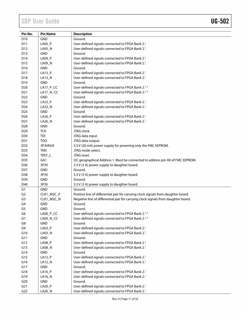
SDP User Guide UG-502
Rev. 0 | Page 11 of 32
Pin No. Pin Name Description D10 GND Ground. D11 LA05_P User-defined signals connected to FPGA Bank 2.1 D12 LA05_N User-defined signals connected to FPGA Bank 2.1 D13 GND Ground. D14 LA09_P User-defined signals connected to FPGA Bank 2.1 D15 LA09_N User-defined signals connected to FPGA Bank 2.1 D16 GND Ground. D17 LA13_P User-defined signals connected to FPGA Bank 2.1 D18 LA13_N User-defined signals connected to FPGA Bank 2.1 D19 GND Ground. D20 LA17_P_CC User-defined signals connected to FPGA Bank 2.1, 2 D21 LA17_N_CC User-defined signals connected to FPGA Bank 2.1, 2 D22 GND Ground. D23 LA23_P User-defined signals connected to FPGA Bank 2.1 D24 LA23_N User-defined signals connected to FPGA Bank 2.1 D25 GND Ground D26 LA26_P User-defined signals connected to FPGA Bank 2.1 D27 LA26_N User-defined signals connected to FPGA Bank 2.1 D28 GND Ground. D29 TCK JTAG clock. D30 TDI JTAG data input. D31 TDO JTAG data output. D32 3P3VAUX 3.3 V (20 mA) power supply for powering only the FMC EEPROM. D33 TMS JTAG mode select. D34 TRST_L JTAG reset. D35 GA1 I2C geographical Address 1. Must be connected to address pin A0 of FMC EEPROM. D36 3P3V 3.3 V (3 A) power supply to daughter board. D37 GND Ground. D38 3P3V 3.3 V (3 A) power supply to daughter board. D39 GND Ground. D40 3P3V 3.3 V (3 A) power supply to daughter board. G1 GND Ground. G2 CLK1_M2C_P Positive line of differential pair for carrying clock signals from daughter board. G3 CLK1_M2C_N Negative line of differential pair for carrying clock signals from daughter board. G4 GND Ground. G5 GND Ground. G6 LA00_P_CC User-defined signals connected to FPGA Bank 2.1, 2 G7 LA00_N_CC User-defined signals connected to FPGA Bank 2.1, 2 G8 GND Ground. G9 LA03_P User-defined signals connected to FPGA Bank 2.1 G10 LA03_N User-defined signals connected to FPGA Bank 2.1 G11 GND Ground. G12 LA08_P User-defined signals connected to FPGA Bank 2.1 G13 LA08_N User-defined signals connected to FPGA Bank 2.1 G14 GND Ground. G15 LA12_P User-defined signals connected to FPGA Bank 2.1 G16 LA12_N User-defined signals connected to FPGA Bank 2.1 G17 GND Ground. G18 LA16_P User-defined signals connected to FPGA Bank 2.1 G19 LA16_N User-defined signals connected to FPGA Bank 2.1 G20 GND Ground. G21 LA20_P User-defined signals connected to FPGA Bank 2.1 G22 LA20_N User-defined signals connected to FPGA Bank 2.1
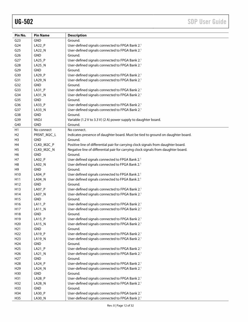
UG-502 SDP User Guide
Rev. 0 | Page 12 of 32
Pin No. Pin Name Description G23 GND Ground. G24 LA22_P User-defined signals connected to FPGA Bank 2.1 G25 LA22_N User-defined signals connected to FPGA Bank 2.1 G26 GND Ground. G27 LA25_P User-defined signals connected to FPGA Bank 2.1 G28 LA25_N User-defined signals connected to FPGA Bank 2.1 G29 GND Ground. G30 LA29_P User-defined signals connected to FPGA Bank 2.1 G31 LA29_N User-defined signals connected to FPGA Bank 2.1 G32 GND Ground. G33 LA31_P User-defined signals connected to FPGA Bank 2.1 G34 LA31_N User-defined signals connected to FPGA Bank 2.1 G35 GND Ground. G36 LA33_P User-defined signals connected to FPGA Bank 2.1 G37 LA33_N User-defined signals connected to FPGA Bank 2.1 G38 GND Ground. G39 VADJ Variable (1.2 V to 3.3 V) (2 A) power supply to daughter board. G40 GND Ground. H1 No connect No connect. H2 PRSNT_M2C_L Indicates presence of daughter board. Must be tied to ground on daughter board. H3 GND Ground. H4 CLK0_M2C_P Positive line of differential pair for carrying clock signals from daughter board. H5 CLK0_M2C_N Negative line of differential pair for carrying clock signals from daughter board. H6 GND Ground. H7 LA02_P User defined signals connected to FPGA Bank 2.1 H8 LA02_N User defined signals connected to FPGA Bank 2.1 H9 GND Ground. H10 LA04_P User defined signals connected to FPGA Bank 2.1 H11 LA04_N User defined signals connected to FPGA Bank 2.1 H12 GND Ground. H13 LA07_P User-defined signals connected to FPGA Bank 2.1 H14 LA07_N User-defined signals connected to FPGA Bank 2.1 H15 GND Ground. H16 LA11_P User-defined signals connected to FPGA Bank 2.1 H17 LA11_N User-defined signals connected to FPGA Bank 2.1 H18 GND Ground. H19 LA15_P User-defined signals connected to FPGA Bank 2.1 H20 LA15_N User-defined signals connected to FPGA Bank 2.1 H21 GND Ground. H22 LA19_P User-defined signals connected to FPGA Bank 2.1 H23 LA19_N User-defined signals connected to FPGA Bank 2.1 H24 GND Ground. H25 LA21_P User-defined signals connected to FPGA Bank 2.1 H26 LA21_N User-defined signals connected to FPGA Bank 2.1 H27 GND Ground. H28 LA24_P User-defined signals connected to FPGA Bank 2.1 H29 LA24_N User-defined signals connected to FPGA Bank 2.1 H30 GND Ground. H31 LA28_P User-defined signals connected to FPGA Bank 2.1 H32 LA28_N User-defined signals connected to FPGA Bank 2.1 H33 GND Ground. H34 LA30_P User-defined signals connected to FPGA bank 2.1 H35 LA30_N User-defined signals connected to FPGA Bank 2.1
SDP User Guide UG-502
Rev. 0 | Page 13 of 32
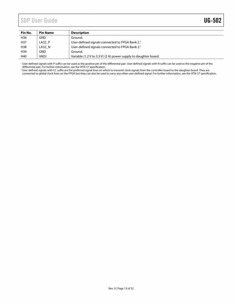
Pin No. Pin Name Description H36 GND Ground. H37 LA32_P User-defined signals connected to FPGA Bank 2.1 H38 LA32_N User-defined signals connected to FPGA Bank 2.1 H39 GND Ground. H40 VADJ Variable (1.2 V to 3.3 V) (2 A) power supply to daughter board. 1 User-defined signals with P suffix can be used as the positive pin of the differential pair. User defined signals with N suffix can be used as the negative pin of the
differential pair. For further information, see the VITA 57 specification. 2 User-defined signals with CC suffix are the preferred signal lines on which to transmit clock signals from the controller board to the daughter board. They are
connected to global clock lines on the FPGA but they can also be used to carry any other user-defined signal. For further information, see the VITA 57 specification.
UG-502 SDP User Guide
Rev. 0 | Page 14 of 32
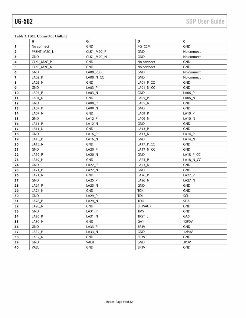
Table 3. FMC Connector Outline H G D C
1 No connect GND PG_C2M GND
2 PRSNT_M2C_L CLK1_M2C_P GND No connect
3 GND CLK1_M2C_N GND No connect
4 CLK0_M2C_P GND No connect GND
5 CLK0_M2C_N GND No connect GND
6 GND LA00_P_CC GND No connect
7 LA02_P LA00_N_CC GND No connect
8 LA02_N GND LA01_P_CC GND
9 GND LA03_P LA01_N_CC GND
10 LA04_P LA03_N GND LA06_P
11 LA04_N GND LA05_P LA06_N
12 GND LA08_P LA05_N GND
13 LA07_P LA08_N GND GND
14 LA07_N GND LA09_P LA10_P
15 GND LA12_P LA09_N LA10_N
16 LA11_P LA12_N GND GND
17 LA11_N GND LA13_P GND
18 GND LA16_P LA13_N LA14_P
19 LA15_P LA16_N GND LA14_N
20 LA15_N GND LA17_P_CC GND
21 GND LA20_P LA17_N_CC GND
22 LA19_P LA20_N GND LA18_P_CC
23 LA19_N GND LA23_P LA18_N_CC
24 GND LA22_P LA23_N GND
25 LA21_P LA22_N GND GND
26 LA21_N GND LA26_P LA27_P
27 GND LA25_P LA26_N LA27_N
28 LA24_P LA25_N GND GND
29 LA24_N GND TCK GND
30 GND LA29_P TDI SCL
31 LA28_P LA29_N TDO SDA
32 LA28_N GND 3P3VAUX GND
33 GND LA31_P TMS GND
34 LA30_P LA31_N TRST_L GA0
35 LA30_N GND GA1 12P0V
36 GND LA33_P 3P3V GND
37 LA32_P LA33_N GND 12P0V
38 LA32_N GND 3P3V GND
39 GND VADJ GND 3P3V
40 VADJ GND 3P3V GND
SDP User Guide UG-502
Rev. 0 | Page 15 of 32
SMA CONNECTORS The SDP-H1 has the PCB footprints for four SMA connectors (Emerson 142-0701-801, Digi-Key J502-ND). J701 and J702 are, respectively, the positive and the negative of a differential pair for supplying an external clock source to the FPGA and they are connected to clock capable pins on the FPGA. J703 and J704 can be used to supply an external trigger to the FPGA but they are not connected to clock capable FPGA pins. J701, J702, J703, and J704 are connected to an FPGA bank supplied by a fixed 3.3 V supply.
POWER The SDP-H1 must be powered using the enclosed 12 V 30 W wall-wart power supply. This 12 V supply is converted, using on-board dc-to-dc switching regulators, to power all on-board systems as well as supply power to any daughter board con-nected to the FMC connector. Table 4 outlines the voltage and currents available to daughter boards connected to the FMC connector (as required by the VITA 57 specification). Note that the maximum allowed power budget for the daughter board is 10 W (for further information, see the VITA 57 specification).
Table 4. FMC Connector Power Supply Capabilities Voltage Supply
Voltage Range
Number Of Pins
Maximum Current Tolerance
VADJ 1.2 V to 3.3 V 2 2 A ±5% 3P3VAUX 3.3 V 1 20 mA ±5% 3P3V 3.3 V 4 3 A ±5% 12P0V 12 V 2 1 A ±5%
The SDP-H1 board also provides 3.3 V at 20 mA on Pin 116 (VIO_+3.3V) to connected daughter boards as the VIO voltage for the daughter board. Pin 5 (USB_VBUS) is connected to an internal 5 V power supply, providing 5 V ±10% as an output of the SDP board.
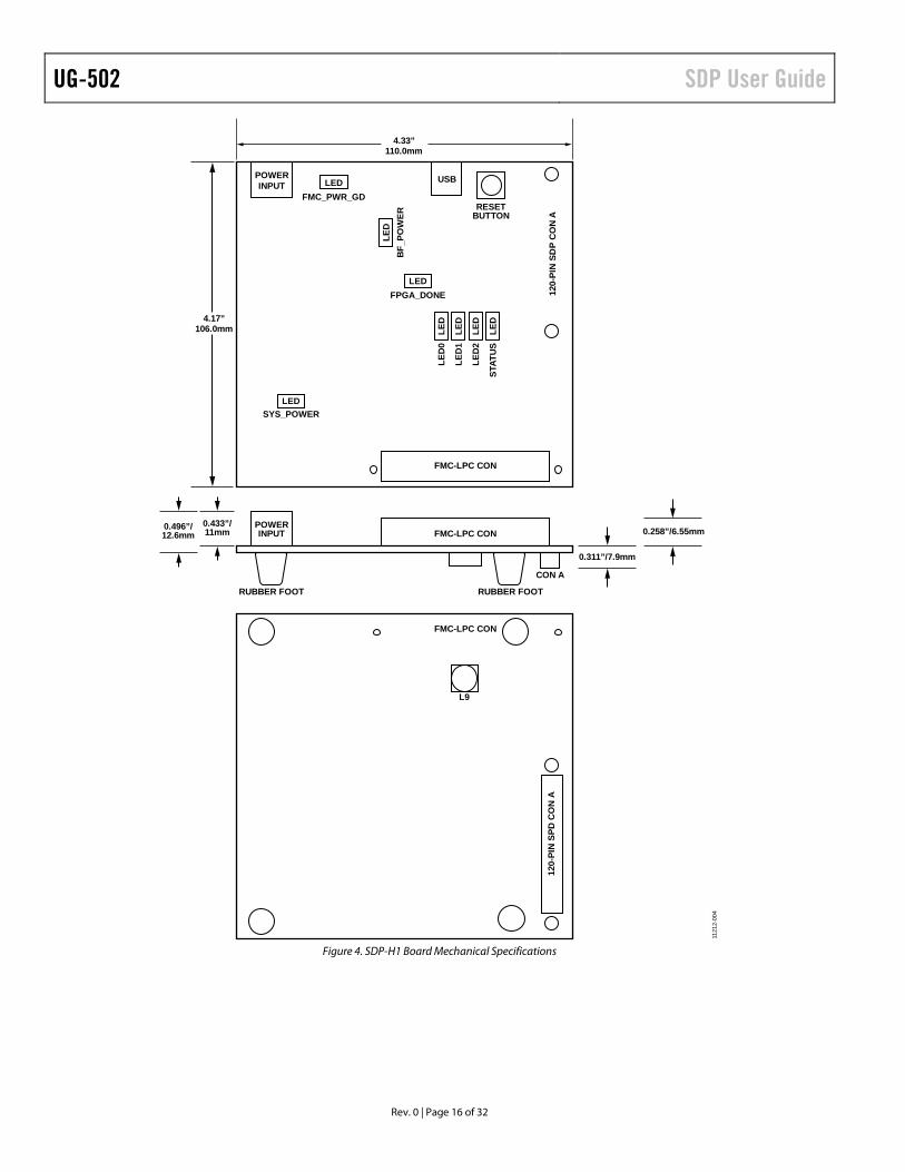
MECHANICAL SPECIFICATIONS The mechanical specifications of the SDP-H1 board are 4.33" × 4.17" (110 mm × 106 mm). The height of the 120-pin connect-ors from the bottom of the board is approximately 0.152" (3.86 mm). The height of the FMC-LPC connector from the top of the board is approximately 0.258” (6.55 mm). The tallest component on the top is the dc power input connector at approximately 0.433" (11 mm) and the tallest component on the bottom is the L9 inductor at approximately 0.157" (4 mm). (The rubber feet on the bottom of the board are 0.311” (7.9 mm) tall.) Refer to Figure 4.
UG-502 SDP User Guide
Rev. 0 | Page 16 of 32
Figure 4. SDP-H1 Board Mechanical Specifications
1121
2-00
4
0.311”/7.9mm
4.33”110.0mm
4.17”106.0mm
0.433”/11mm0.496”/
12.6mm 0.258”/6.55mm
POWERINPUT
POWERINPUT
RUBBER FOOT RUBBER FOOT
USB
RESETBUTTON
120-
PIN
SD
P C
ON
A
LEDFMC_PWR_GD
LEDFPGA_DONE
FMC-LPC CON
120-
PIN
SPD
CO
N A
FMC-LPC CON
FMC-LPC CON
L9
CON A
SYS_POWER
LED
LED
LED
LED
LED
LED
LED
0
LED
1
LED
2
STAT
US
BF_
POW
ER
SDP User Guide UG-502
Rev. 0 | Page 17 of 32
SCHEMATICS This section provides the schematic drawings for the EVAL-SDP-CH1Z board. The schematic pages include:
• SDP-H1—Blackfin Power • SDP-H1—Blackfin Memory • SDP-H1—Blackfin Clocks_USB • SDP-H1—Blackfin I/O • SDP-H1—Blackfin Connector A • SDP-H1—FPGA Bank 0-Blackfin • SDP-H1—FPGA Bank 1-SRAM • SDP-H1—FPGA Bank 2-FMC • SDP-H1—FPGA Bank 3-SDRAM • SDP-H1—FPGA Power • SDP-H1—Power Supply Part 1 • SDP-H1—Power Supply Part 2 • SDP-H1—Power Supply Part 3
UG-502 SDP User Guide
Rev. 0 | Page 18 of 32
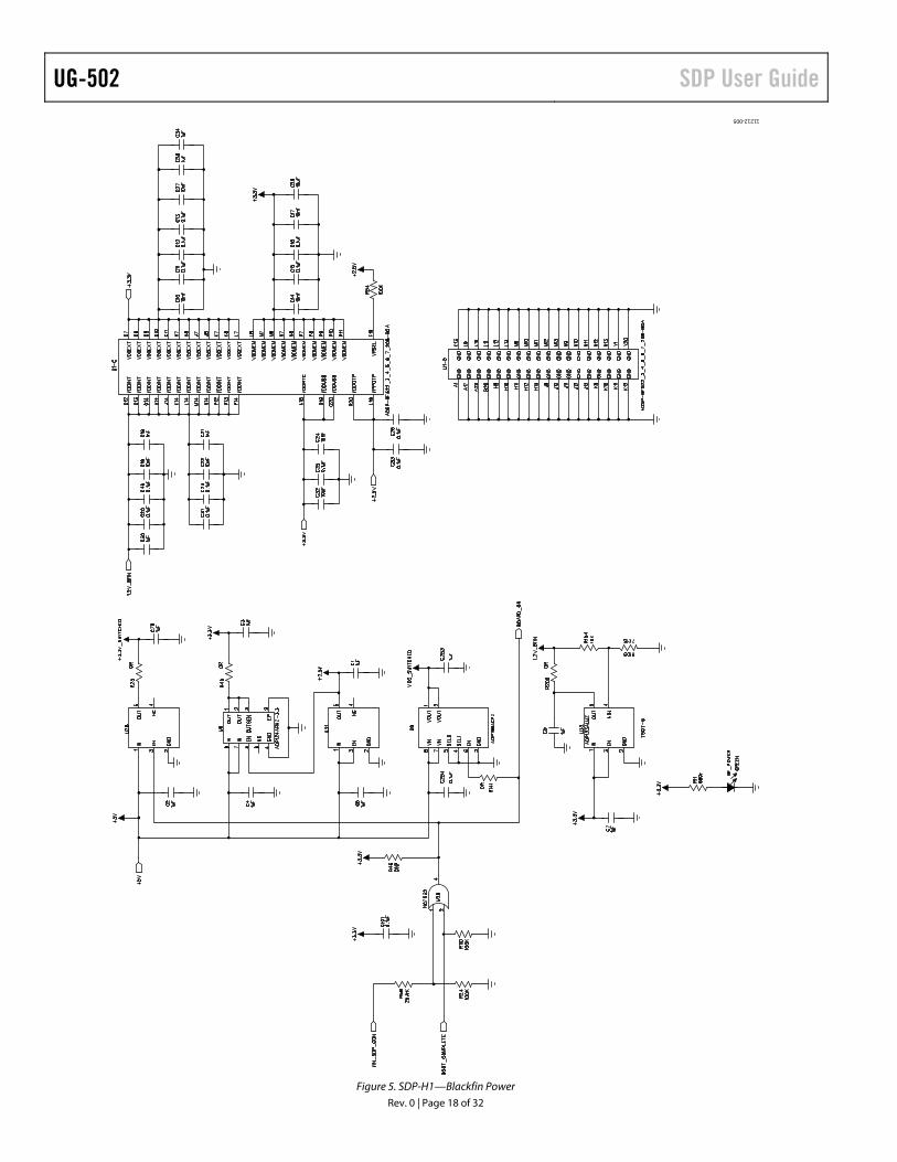
Figure 5. SDP-H1—Blackfin Power
11212-005
SDP User Guide UG-502
Rev. 0 | Page 19 of 32
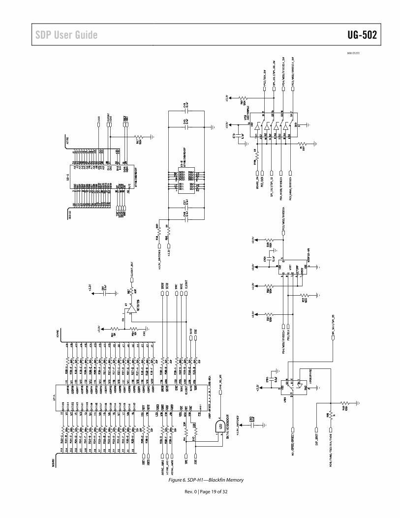
Figure 6. SDP-H1—Blackfin Memory
11212-006
UG-502 SDP User Guide
Rev. 0 | Page 20 of 32
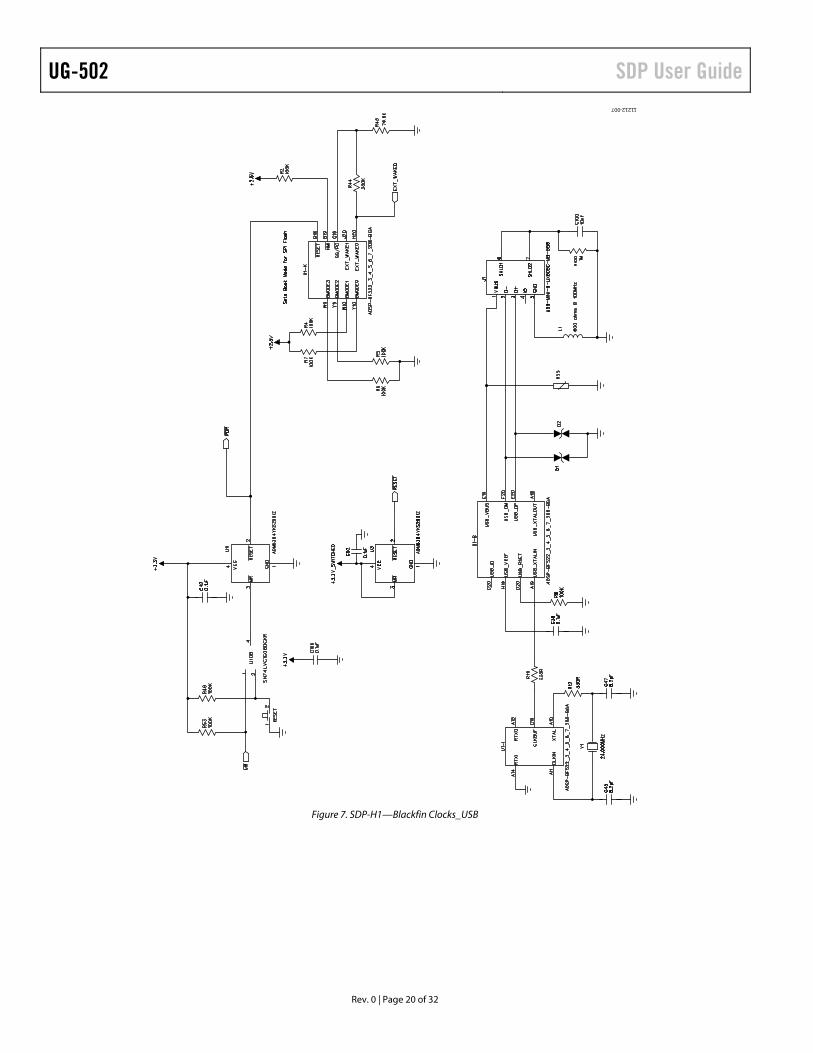
Figure 7. SDP-H1—Blackfin Clocks_USB
11212-007
SDP User Guide UG-502
Rev. 0 | Page 21 of 32
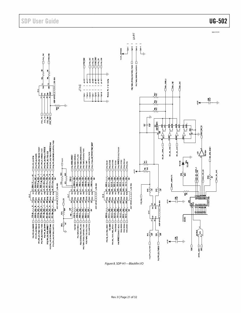
Figure 8. SDP-H1—Blackfin I/O
11212-008
UG-502 SDP User Guide
Rev. 0 | Page 22 of 32
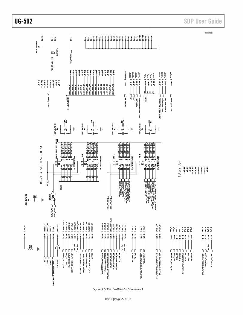
Figure 9. SDP-H1—Blackfin Connector A
11212-009
SDP User Guide UG-502
Rev. 0 | Page 23 of 32
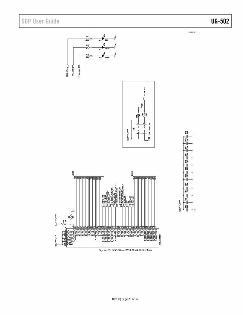
Figure 10. SDP-H1—FPGA Bank 0-Blackfin
11212-010
UG-502 SDP User Guide
Rev. 0 | Page 24 of 32
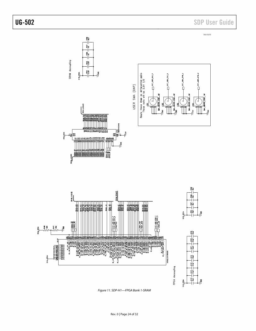
Figure 11. SDP-H1—FPGA Bank 1-SRAM
11212-011
SDP User Guide UG-502
Rev. 0 | Page 25 of 32
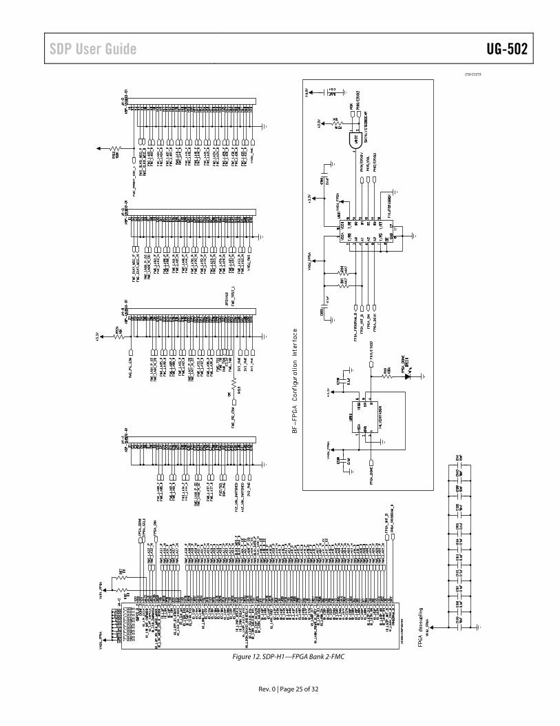
Figure 12. SDP-H1—FPGA Bank 2-FMC
11212-012
UG-502 SDP User Guide
Rev. 0 | Page 26 of 32
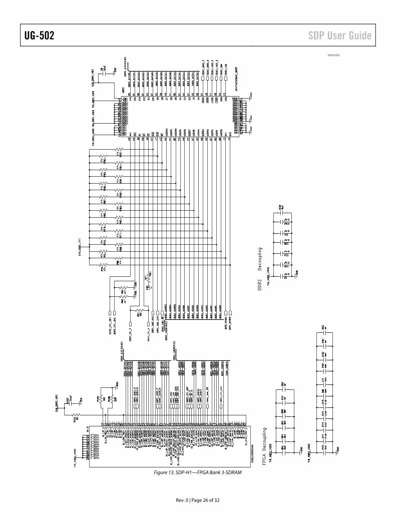
Figure 13. SDP-H1—FPGA Bank 3-SDRAM
11212-013
SDP User Guide UG-502
Rev. 0 | Page 27 of 32
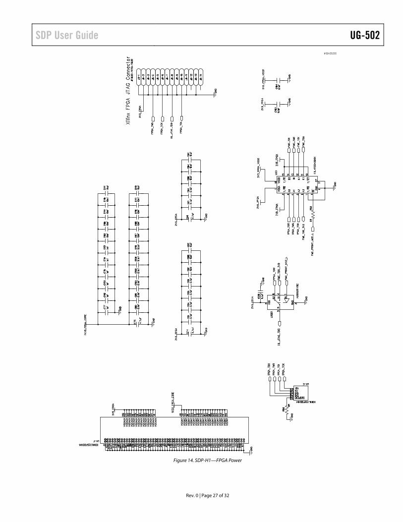
Figure 14. SDP-H1—FPGA Power
11212-014
UG-502 SDP User Guide
Rev. 0 | Page 28 of 32
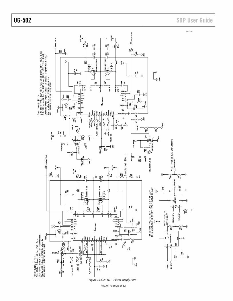
Figure 15. SDP-H1—Power Supply Part 1
11212-015
SDP User Guide UG-502
Rev. 0 | Page 29 of 32
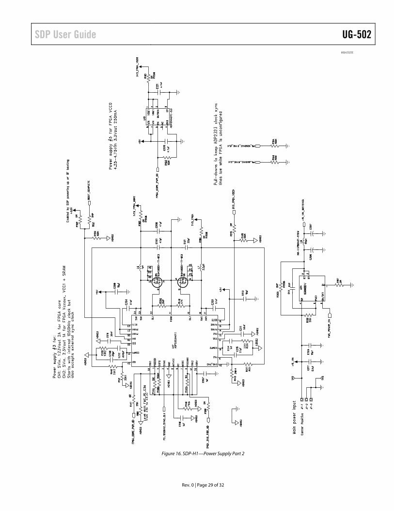
Figure 16. SDP-H1—Power Supply Part 2
11212-016
UG-502 SDP User Guide
Rev. 0 | Page 30 of 32
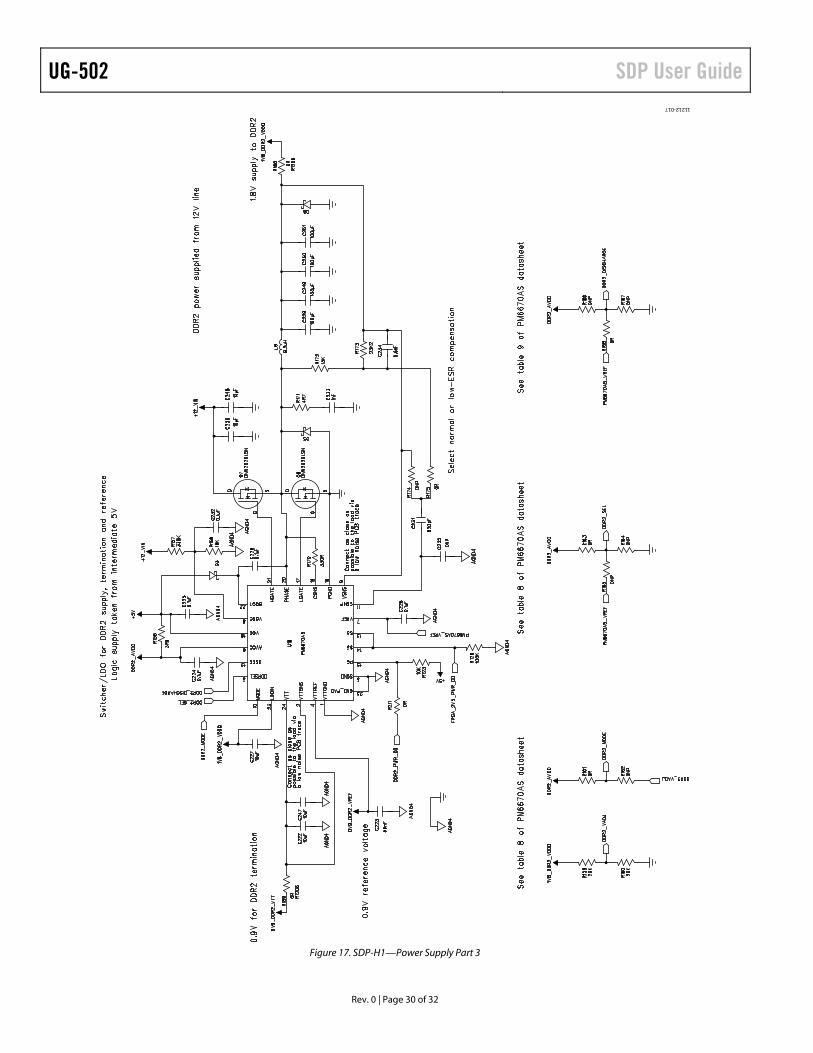
Figure 17. SDP-H1—Power Supply Part 3
11212-017
SDP User Guide UG-502
Rev. 0 | Page 31 of 32
NOTES
UG-502 SDP User Guide
Rev. 0 | Page 32 of 32
NOTES
ESD Caution ESD (electrostatic discharge) sensitive device. Charged devices and circuit boards can discharge without detection. Although this product features patented or proprietary protection circuitry, damage may occur on devices subjected to high energy ESD. Therefore, proper ESD precautions should be taken to avoid performance degradation or loss of functionality.
Legal Terms and Conditions By using the evaluation board discussed herein (together with any tools, components documentation or support materials, the “Evaluation Board”), you are agreeing to be bound by the terms and conditions set forth below (“Agreement”) unless you have purchased the Evaluation Board, in which case the Analog Devices Standard Terms and Conditions of Sale shall govern. Do not use the Evaluation Board until you have read and agreed to the Agreement. Your use of the Evaluation Board shall signify your acceptance of the Agreement. This Agreement is made by and between you (“Customer”) and Analog Devices, Inc. (“ADI”), with its principal place of business at One Technology Way, Norwood, MA 02062, USA. Subject to the terms and conditions of the Agreement, ADI hereby grants to Customer a free, limited, personal, temporary, non-exclusive, non-sublicensable, non-transferable license to use the Evaluation Board FOR EVALUATION PURPOSES ONLY. Customer understands and agrees that the Evaluation Board is provided for the sole and exclusive purpose referenced above, and agrees not to use the Evaluation Board for any other purpose. Furthermore, the license granted is expressly made subject to the following additional limitations: Customer shall not (i) rent, lease, display, sell, transfer, assign, sublicense, or distribute the Evaluation Board; and (ii) permit any Third Party to access the Evaluation Board. As used herein, the term “Third Party” includes any entity other than ADI, Customer, their employees, affiliates and in-house consultants. The Evaluation Board is NOT sold to Customer; all rights not expressly granted herein, including ownership of the Evaluation Board, are reserved by ADI. CONFIDENTIALITY. This Agreement and the Evaluation Board shall all be considered the confidential and proprietary information of ADI. Customer may not disclose or transfer any portion of the Evaluation Board to any other party for any reason. Upon discontinuation of use of the Evaluation Board or termination of this Agreement, Customer agrees to promptly return the Evaluation Board to ADI. ADDITIONAL RESTRICTIONS. Customer may not disassemble, decompile or reverse engineer chips on the Evaluation Board. Customer shall inform ADI of any occurred damages or any modifications or alterations it makes to the Evaluation Board, including but not limited to soldering or any other activity that affects the material content of the Evaluation Board. Modifications to the Evaluation Board must comply with applicable law, including but not limited to the RoHS Directive. TERMINATION. ADI may terminate this Agreement at any time upon giving written notice to Customer. Customer agrees to return to ADI the Evaluation Board at that time. LIMITATION OF LIABILITY. THE EVALUATION BOARD PROVIDED HEREUNDER IS PROVIDED “AS IS” AND ADI MAKES NO WARRANTIES OR REPRESENTATIONS OF ANY KIND WITH RESPECT TO IT. ADI SPECIFICALLY DISCLAIMS ANY REPRESENTATIONS, ENDORSEMENTS, GUARANTEES, OR WARRANTIES, EXPRESS OR IMPLIED, RELATED TO THE EVALUATION BOARD INCLUDING, BUT NOT LIMITED TO, THE IMPLIED WARRANTY OF MERCHANTABILITY, TITLE, FITNESS FOR A PARTICULAR PURPOSE OR NONINFRINGEMENT OF INTELLECTUAL PROPERTY RIGHTS. IN NO EVENT WILL ADI AND ITS LICENSORS BE LIABLE FOR ANY INCIDENTAL, SPECIAL, INDIRECT, OR CONSEQUENTIAL DAMAGES RESULTING FROM CUSTOMER’S POSSESSION OR USE OF THE EVALUATION BOARD, INCLUDING BUT NOT LIMITED TO LOST PROFITS, DELAY COSTS, LABOR COSTS OR LOSS OF GOODWILL. ADI’S TOTAL LIABILITY FROM ANY AND ALL CAUSES SHALL BE LIMITED TO THE AMOUNT OF ONE HUNDRED US DOLLARS ($100.00). EXPORT. Customer agrees that it will not directly or indirectly export the Evaluation Board to another country, and that it will comply with all applicable United States federal laws and regulations relating to exports. GOVERNING LAW. This Agreement shall be governed by and construed in accordance with the substantive laws of the Commonwealth of Massachusetts (excluding conflict of law rules). Any legal action regarding this Agreement will be heard in the state or federal courts having jurisdiction in Suffolk County, Massachusetts, and Customer hereby submits to the personal jurisdiction and venue of such courts. The United Nations Convention on Contracts for the International Sale of Goods shall not apply to this Agreement and is expressly disclaimed.
©2013 Analog Devices, Inc. All rights reserved. Trademarks and registered trademarks are the property of their respective owners. UG11212-0-4/13(0)