Embed Size (px)
Citation preview

One Technology Way · P.O. Box 9106 · Norwood, MA 02062-9106 · Tel: 781.329.4700 · Fax: 781.461.3113 · www.analog.com
Rev 13 May 2013 17:57 | Page 1
EVALUATING THE AD9653/AD9253/AD9633ANALOG-TO-DIGITAL CONVERTERS
Preface
This user guide describes the AD9653, AD9253 and AD9633 evaluation boards, AD9653-125EBZ,AD9253-125EBZ and AD9633-125EBZ, which provide all of the support circuitry required to operatethese parts in their various modes and configurations. The application software used to interface withthe devices is also described.
The AD9653 AD9253 and AD9633 data sheets provide additional information and should be consultedwhen using the evaluation board. All documents and software tools are available atwww.analog.com/hsadcevalboard. For additional information or questions, send an email [email protected].
Typical Measurement Setup
Figure 1. Evaluation Board Connection—AD9653-125EBZ, AD9253-125EBZ or AD9633-125EBZ (on Left)and HSC-ADC-EVALCZ (on Right)
Rev 13 May 2013 17:57 | Page 2
Features
Full featured evaluation board for the AD9653/AD9253/AD9633●
SPI interface for setup and control●
External, on-board oscillator, or AD9517 clocking option●
Balun/transformer or amplifier input drive option●
On-board LDO regulator needing a single external 6 V, 2 A dc supply●
VisualAnalog® and SPI controller software interfaces●
Helpful Documents
AD9653, AD9253 or AD9633 data sheet●
High speed ADC FIFO evaluation kit (HSC-ADC-EVALCZ)●
AN-905 Application Note, VisualAnalog Converter Evaluation Tool Version 1.0 User Manual●
AN-878 Application Note, High Speed ADC SPI Control Software●
AN-877 Application Note, Interfacing to High Speed ADCs via SPI●
AN-835 Application Note, Understanding ADC Testing and Evaluation●
Design and Integration Files
Schematics, layout files, bill of materials●
Equipment Needed
Analog signal source and antialiasing filter●
Sample clock source (if not using the on-board oscillator)●
2 switching power supplies (6.0 V, 2.5 A), CUI EPS060250UH-PHP-SZ provided●
PC running Windows®●
USB 2.0 port●
AD9653-125EBZ, AD9253-125EBZ or AD9633-125EBZ board●
HSC-ADC-EVALCZ FPGA-based data capture kit●
Getting Started
This section provides quick start procedures for using the AD9653-125EBZ, AD9253-125EBZ orAD9633-125EBZ board. Both the default and optional settings are described.

Rev 13 May 2013 17:57 | Page 3
Configuring the Board
Before using the software for testing, configure the evaluation board as follows:
Connect the evaluation board to the data capture board, as shown in Figure 1.1.Connect one 6 V, 2.5 A switching power supply (such as the CUI, Inc., EPS060250UH-PHP-SZ that is2.supplied) to the AD9653-125EBZ, AD9253-125EBZ or AD9633-125EBZ.Connect one 6 V, 2.5 A switching power supply (such as the supplied CUI EPS060250UH-PHP-SZ) to3.the HSC-ADC-EVALCZ board.Connect the HSC-ADC-EVALCZ board (J6) to the PC using a USB cable.4.On the ADC evaluation board, confirm that the jumpers are installed as shown in Figure 2 and5.Table 1.On the ADC evaluation board, use a clean signal generator with low phase noise to provide an6.input signal to the desired A and/or B channel(s). Use a 1 m, shielded, RG-58, 50 Ω coaxial cable toconnect the signal generator. For best results, use a narrow-band, band-pass filter with 50 Ωterminations and an appropriate center frequency. (Analog Devices, Inc., uses TTE, Allen Avionics,and K&L band-pass filters.)
Evaluation Board Hardware
The evaluation board provides the support circuitry required to operate the AD9653, AD9253 andAD9633 in their various modes and configurations. Figure 1 shows the typical bench characterizationsetup used to evaluate AC performance. It is critical that the signal sources used for the analog inputand clock have very low phase noise (<1 ps rms jitter) to realize the optimum performance of thesignal chain. Proper filtering of the analog input signal to remove harmonics and lower the integratedor broadband noise at the input is necessary to achieve the specified noise performance.
See the Getting Started section to get started, and visit UG-328 Design Support for the completeschematics and layout diagrams. These diagrams demonstrate the routing and grounding techniquesthat should be applied at the system level when designing application boards using these converters.
Power Supplies
This evaluation board comes with a wall-mountable switching power supply that provides a 6 V, 2 Amaximum output. Connect the supply to a 100 V ac to 240 V ac, 47 Hz to 63 Hz wall outlet. Theoutput from the supply is provided through a 2.1 mm inner diameter jack that connects to the printedcircuit board (PCB) at P101. The 6 V supply is fused and conditioned on the PCB before connecting tothe low dropout linear regulators that supply the proper bias to each of the various sections on theboard.
The evaluation board can be powered in a nondefault condition using external bench power supplies.To do this, remove the E101, E102, E103 and E104 ferrite beads to disconnect the outputs from the
Rev 13 May 2013 17:57 | Page 4
on-board LDOs. This enables the user to bias each section of the board individually. Use P102 andP103 to connect a different supply for each section. A 1.8 V, 0.5 A supply is needed for 1.8V_AVDDand 1.8V_DRVDD. Although the power supply requirements are the same for AVDD and DRVDD, it isrecommended that separate supplies be used for both analog and digital domains. The SPI and itslevel shifters and alternate clock options require a separate 3.3 V, 0.5 A analog supply.
Two additional supplies, 5V_AVDD and 3V_AVDD, are used to bias the optional input path amplifiersand optional AD9517-3 clock chip. If used, these supplies should each have 0.5 A current capability.
Input Signals
When connecting the ADC clock and analog source, use clean signal generators with low phase noise,such as the Rohde & Schwarz SMA, or HP 8644B signal generators or an equivalent. Use a 1 mshielded, RG-58, 50 Ω coaxial cable for connecting to the evaluation board. Enter the desiredfrequency and amplitude (see the Specifications section in the data sheet of the respective part).When connecting the analog input source, use of a multipole, narrow-band band-pass filter with 50 Ωterminations is recommended. Analog Devices uses band-pass filters from TTE and K&L Microwave,Inc. Connect the filters directly to the evaluation board.
If an external clock source is used, it should also be supplied with a clean signal generator aspreviously specified. Analog Devices evaluation boards typically can accept ~2.8 V p-p or 13 dBm sinewave input for the clock.
Output Signals
The default setup uses the Analog Devices high speed converter evaluation platform (HSC-ADC-EVALCZ) for data capture. The serial LVDS outputs from the ADC are routed to ConnectorP1002 using 100 Ω differential traces. For more information on the data capture board and its optionalsettings, visit www.analog.com/hsadcevalboard.
Jumper Settings
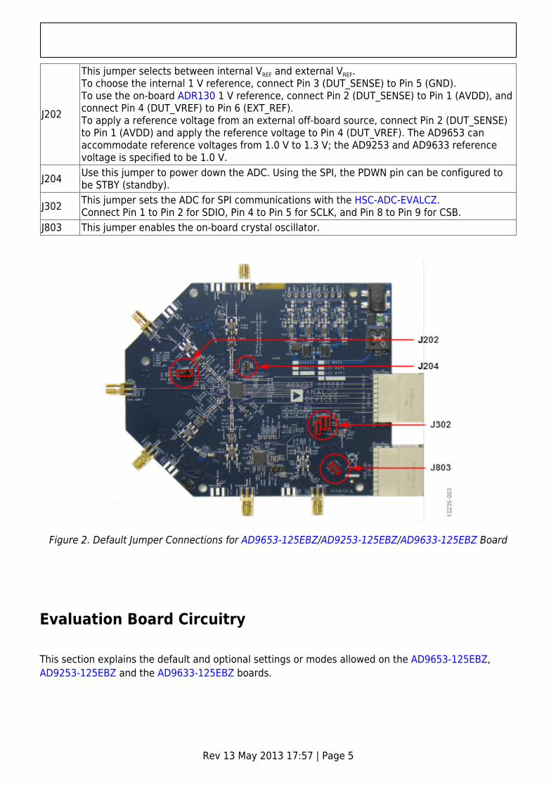
Set the jumper settings/link options on the evaluation board for the required operating modes beforepowering on the board. The functions of the jumpers are described in Table 1. Figure 2 shows thedefault jumper settings.
Table 1. Jumper SettingsJumper Description
Rev 13 May 2013 17:57 | Page 5
J202
This jumper selects between internal VREF and external VREF.To choose the internal 1 V reference, connect Pin 3 (DUT_SENSE) to Pin 5 (GND).To use the on-board ADR130 1 V reference, connect Pin 2 (DUT_SENSE) to Pin 1 (AVDD), andconnect Pin 4 (DUT_VREF) to Pin 6 (EXT_REF).To apply a reference voltage from an external off-board source, connect Pin 2 (DUT_SENSE)to Pin 1 (AVDD) and apply the reference voltage to Pin 4 (DUT_VREF). The AD9653 canaccommodate reference voltages from 1.0 V to 1.3 V; the AD9253 and AD9633 referencevoltage is specified to be 1.0 V.
J204 Use this jumper to power down the ADC. Using the SPI, the PDWN pin can be configured tobe STBY (standby).
J302 This jumper sets the ADC for SPI communications with the HSC-ADC-EVALCZ.Connect Pin 1 to Pin 2 for SDIO, Pin 4 to Pin 5 for SCLK, and Pin 8 to Pin 9 for CSB.
J803 This jumper enables the on-board crystal oscillator.
Figure 2. Default Jumper Connections for AD9653-125EBZ/AD9253-125EBZ/AD9633-125EBZ Board
Evaluation Board Circuitry
This section explains the default and optional settings or modes allowed on the AD9653-125EBZ,AD9253-125EBZ and the AD9633-125EBZ boards.
Rev 13 May 2013 17:57 | Page 6
Power
Plug the switching power supply into a wall outlet rated at 100 V ac to 240 V ac, 47 Hz to 63 Hz.Connect the DC output connector to P101 on the evaluation board.
Analog Input
The four channel inputs on the evaluation board are set up for a double balun-coupled analog inputwith a 50 Ω impedance. The default analog input configuration supports analog input frequencies ofup to ~200 MHz.
VREF
The default VREF configuration is to connect the SENSE pin to AGND for internal VREF operation. Thisis done by connecting Pin 3 to Pin 5 on Header J202. An external reference voltage can be provided tothe AD9653, AD9253 and AD9633. Connecting Pin 2 to Pin 1 on Header J202 puts the ADC in a modewhere it requires a reference voltage from an external source. The external on-board 1.0 V referenceis provided by the ADR130. This external reference can be connected to the ADC by connecting Pin 4to Pin 6 on Header J202. Alternatively, if an external off-board reference is desired, connect Pin 2 toPin1 on Header J202 and apply the reference voltage directly to Pin 4 of Header J202. The AD9653 canaccommodate reference voltages from 1.0 V to 1.3 V; the AD9253 and AD9633 reference voltage isspecified to be 1.0 V.
RBIAS
RBIAS has a default setting of 10 kΩ (R205) to ground and is used to set the ADC core bias current.Note that using a resistor value other than a 10 kΩ, 1% resistor for RBIAS may degrade theperformance of the device.
Clock
The default clock input circuit is derived from a simple transformer-coupled circuit using a highbandwidth 1:1 impedance ratio transformer (T801/T802) that adds a low amount of jitter to the clockpath. The clock input is 50 Ω terminated and ac-coupled to handle single-ended sine wave types ofinputs. The transformer converts the single-ended input to a differential signal that is clipped by

Rev 13 May 2013 17:57 | Page 7
CR801 before entering the ADC clock inputs. The AD9653, AD9253 and AD9633 ADCs are equippedwith an internal 8:1 clock divider to facilitate usage with higher frequency clocks. When using theinternal divider and a higher input clock frequency, remove CR801 to preserve the slew rate of theclock signal.
The AD9653-125EBZ, AD9253-125EBZ and AD9633-125EBZ boards are set up to be clocked throughthe transformer-coupled input network from the crystal oscillator, Y801. This oscillator is a low phasenoise oscillator from Valpey Fisher (VFAC3-BHL-125MHz). If a different clock source is desired, removeC810 (optional) and Jumper J803 to disable the oscillator from running and connect the external clocksource to the SMA connector, J802 (labeled CLK+).
PDWN
To enable the power-down feature, add a shorting jumper across J204 at Pin 1 and Pin 2 to connectthe PDWN pin to DRVDD.
Modes of Operation
Standalone (PIN) Mode
The AD9653/AD9253/AD9633 ADCs can operate in pin mode if there is no need to program andchange the default modes of operation via the SPI. For applications that do not require SPI modeoperation, the CSB pin is tied to AVDD, and the SDIO/OLM pin controls the output lane mode. Table 2and Table 3 specify the settings for pin mode operation.
Table 2. Output Lane Mode (OLM) Pin Settings
OLM Pin Voltage Output ModeAVDD (Default) Two-lane. 1× frame, 16-bit serial outputGND One-lane. 1× frame, 16-bit serial output
Table 3. Digital Test Pattern (DTP) Pin Settings
Seected DTP Output Mode Resulting D0±x and D1±xNormal Operation 10 kΩ to AGND Normal operationDTP AVDD 1000 0000 0000 0000
Additional information on the lane modes is provided in the AD9653, AD9253 and AD9633 data sheets.
Rev 13 May 2013 17:57 | Page 8
Default Mode
To operate the device under test (DUT) using the SPI, follow the jumper settings for J302 as shown inTable 1.
How To Use The Software For Testing
Setting up the ADC Data Capture
After configuring the board, set up the ADC data capture using the following steps:
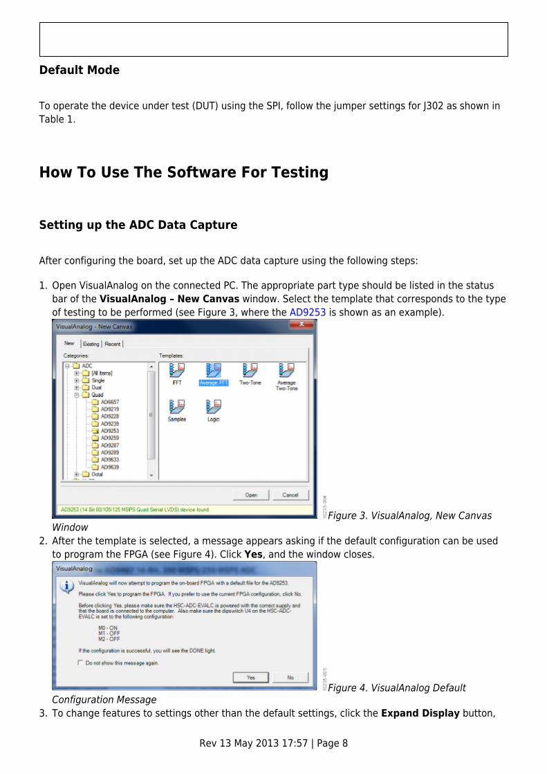
Open VisualAnalog on the connected PC. The appropriate part type should be listed in the status1.bar of the VisualAnalog – New Canvas window. Select the template that corresponds to the typeof testing to be performed (see Figure 3, where the AD9253 is shown as an example).
Figure 3. VisualAnalog, New CanvasWindowAfter the template is selected, a message appears asking if the default configuration can be used2.to program the FPGA (see Figure 4). Click Yes, and the window closes.
Figure 4. VisualAnalog DefaultConfiguration MessageTo change features to settings other than the default settings, click the Expand Display button,3.

Rev 13 May 2013 17:57 | Page 9
located on the bottom right corner of the window (see Figure 5), to see what is shown in Figure 6.Change the features and capture settings by consulting the detailed instructions in the AN-9054.Application Note, VisualAnalog Converter Evaluation Tool Version 1.0 User Manual. After thechanges are made to the capture settings, click the Collapse Display button.
Figure 5. VisualAnalog Window Toolbar, Collapsed Display
Figure 6. VisualAnalog, Main Window Expanded Display
Evaluation And Test
Setting up the SPI Controller Software
After the ADC data capture board setup is complete, set up the SPI controller software using thefollowing procedure:
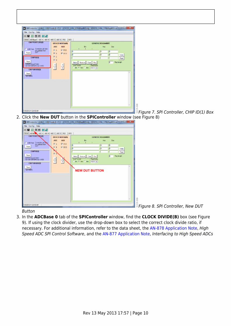
Open the SPI controller software by going to the Start menu or by double-clicking the1.SPIController software desktop icon. If prompted for a configuration file, select the appropriateone. If not, check the title bar of the window to determine which configuration is loaded. Ifnecessary, choose Cfg Open from the File menu and select the appropriate file based on yourpart type. Note that the CHIP ID(1) box should be filled to indicate whether the correct SPIcontroller configuration file is loaded (see Figure 7).
Rev 13 May 2013 17:57 | Page 10
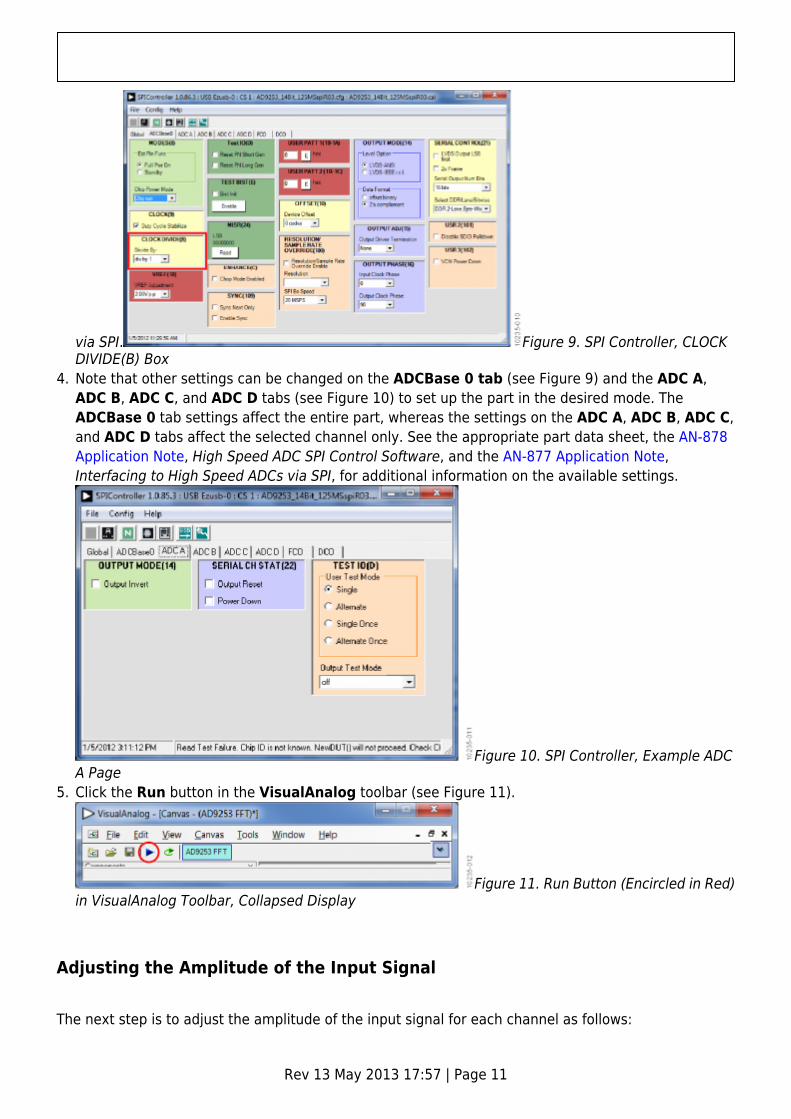
Figure 7. SPI Controller, CHIP ID(1) BoxClick the New DUT button in the SPIController window (see Figure 8)2.
Figure 8. SPI Controller, New DUTButtonIn the ADCBase 0 tab of the SPIController window, find the CLOCK DIVIDE(B) box (see Figure3.9). If using the clock divider, use the drop-down box to select the correct clock divide ratio, ifnecessary. For additional information, refer to the data sheet, the AN-878 Application Note, HighSpeed ADC SPI Control Software, and the AN-877 Application Note, Interfacing to High Speed ADCs
Rev 13 May 2013 17:57 | Page 11
via SPI. Figure 9. SPI Controller, CLOCKDIVIDE(B) BoxNote that other settings can be changed on the ADCBase 0 tab (see Figure 9) and the ADC A,4.ADC B, ADC C, and ADC D tabs (see Figure 10) to set up the part in the desired mode. TheADCBase 0 tab settings affect the entire part, whereas the settings on the ADC A, ADC B, ADC C,and ADC D tabs affect the selected channel only. See the appropriate part data sheet, the AN-878Application Note, High Speed ADC SPI Control Software, and the AN-877 Application Note,Interfacing to High Speed ADCs via SPI, for additional information on the available settings.
Figure 10. SPI Controller, Example ADCA PageClick the Run button in the VisualAnalog toolbar (see Figure 11).5.
Figure 11. Run Button (Encircled in Red)in VisualAnalog Toolbar, Collapsed Display
Adjusting the Amplitude of the Input Signal
The next step is to adjust the amplitude of the input signal for each channel as follows:

Rev 13 May 2013 17:57 | Page 12
Adjust the amplitude of the input signal so that the fundamental is at the desired level. Examine1.the Fund Power reading in the left panel of the VisualAnalog Graph - AD9253 FFT window
(see Figure 12). Figure 12. GraphWindow of VisualAnalog Repeat this procedure for Channel B, Channel C, and Channel D.2.Click the disk icon within the VisualAnalog Graph - AD9253 FFT window to save the3.performance plot data as a .csv formatted file. See Figure 13 for an example.
Figure 13. Typical FFT, AD9253
Troubleshooting Tips
If the FFT plot appears abnormal, do the following:
If you see an abnormal noise floor, go to the ADCBase0 tab of the SPIController window and●
toggle the Chip Power Mode in MODES(8) from Chip Run to Reset and back.If you see a normal noise floor when you disconnect the signal generator from the analog input, be●
Rev 13 May 2013 17:57 | Page 13
sure that you are not overdriving the ADC. Reduce the input level if necessary.In VisualAnalog, click the Settings icon in the Input Formatter block. Check that Number●
Format is set to the correct encoding (twos complement by default). Repeat for the other channels.
If the FFT appears normal but the performance is poor, check the following:
Make sure that an appropriate filter is used on the analog input.●
Make sure that the signal generators for the clock and the analog input are clean (low phase noise).●
Change the analog input frequency slightly if noncoherent sampling is being used.●
Make sure that the SPI configuration file matches the product being evaluated.●
If the FFT window remains blank after Run in VisualAnalog (see Figure 11) is clicked, do the following:
Make sure that the evaluation board is securely connected to the HSC-ADC-EVALCZ board.●
Make sure that the FPGA has been programmed by verifying that the DONE LED is illuminated on●
the HSC-ADC-EVALCZ board. If this LED is not illuminated, make sure that the U4 switch on theboard is in the correct position for USB CONFIG.Make sure that the correct FPGA program was installed by clicking the Settings icon in the ADC●
Data Capture block in VisualAnalog. Then select the FPGA tab and verify that the proper FPGA binfile is selected for the part.
If VisualAnalog indicates that the FIFO Capture timed out, do the following:
Make sure that all power and USB connections are secure.●
Probe the DCO signal at P1002 (Pin A10 and/or Pin B10) on the evaluation board, and confirm that a●
clock signal is present at the ADC sampling rate.
© Analog Devices, Inc. All rights reserved. Trademarks andregistered trademarks are the property of their respective owners. www.analog.com