Embed Size (px)
Citation preview
AN-1535APPLICATION NOTE
One Technology Way • P.O. Box 9106 • Norwood, MA 02062-9106, U.S.A. • Tel: 781.329.4700 • Fax: 781.461.3113 • www.analog.com
ADuM4135 Gate Driver Performance Driving SiC Power Switches
by Hans Brueggemann
Rev. 0 | Page 1 of 12
INTRODUCTION In solar photovoltaics (PV) and energy storage applications, there is a trend towards increased power density along with the ever present need of improved efficiency. A solution to this problem comes in the form of silicon carbide (SiC) power devices.
SiC devices are wide band-gap devices that can operate at an increased voltage of >120 V dc and tend to have a low drain source impedance (RDSON). With some devices having an RDSON as low as 8 mΩ, these devices also fill the need for reduced conduction losses and therefore increased efficiency. SiC devices can also exhibit fast switching speeds of >100 kHz with low parasitic capacitance and associated charge during switching. However, disadvantages include a requirement for higher common-mode transient immunity (CMTI) greater than 100 kV/μs required for gate drivers. Another disadvantage is that higher switching across the drain source of the SiC can
lead to ringing at the gate of the device. These disadvantages can cause problems when driving higher voltage SiC devices, where significant power density improvement can be achieved by their implementation.
One combination of gate driver and SiC that can solve these problems is the ADuM4135 and the SiC module, as specified in Table 1. The power module is a half bridge SiC device with a 1200 V collector emitter voltage rating and a continuous current capability of 75 A. Its gate source voltage (VGS) rating is +20 V to −10 V. It has an isolation rating of 2.5 kV for 1 min. The input capacitance (CISS) of the modules is 4.2 nF, with a reverse recovery time of 25 ns.
The ADuM4135 gate driver is a single-channel device with a typical drive capability of 7 A source/sink at a 25 V operating voltage (VDD to VSS). It has a minimum CMTI of 100 kV/μs.
164
40-0
01
Figure 1. ADuM4135 Gate Drive Module
AN-1535 Application Note
Rev. 0 | Page 2 of 12
TABLE OF CONTENTS Introduction ...................................................................................... 1 Revision History ............................................................................... 2 Experimental Setup .......................................................................... 3
Measuring Gate Drive Signals .................................................... 3 Gate Voltage Control .................................................................... 4 Decoupling the DC Link ............................................................. 4
Test Setup ........................................................................................... 5
Electrical Setup ..............................................................................5 Test Results .........................................................................................6
No Load Testing ............................................................................6 Load Testing ...................................................................................8
Schematic ......................................................................................... 11 Conclusion....................................................................................... 12
REVISION HISTORY 1/2018—Revision 0: Initial Version
Application Note AN-1535
Rev. 0 | Page 3 of 12
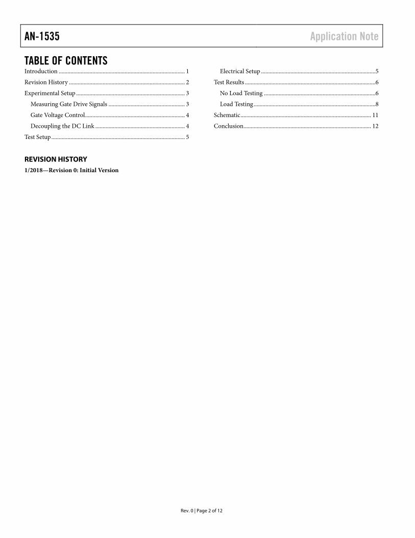
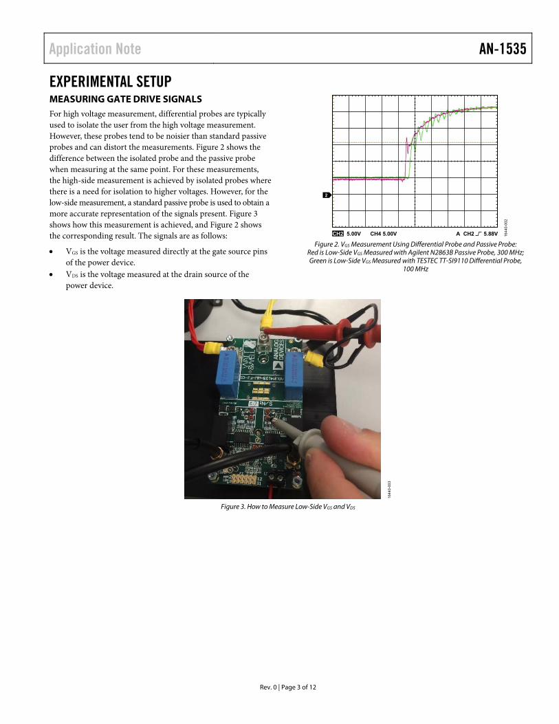
EXPERIMENTAL SETUP MEASURING GATE DRIVE SIGNALS For high voltage measurement, differential probes are typically used to isolate the user from the high voltage measurement. However, these probes tend to be noisier than standard passive probes and can distort the measurements. Figure 2 shows the difference between the isolated probe and the passive probe when measuring at the same point. For these measurements, the high-side measurement is achieved by isolated probes where there is a need for isolation to higher voltages. However, for the low-side measurement, a standard passive probe is used to obtain a more accurate representation of the signals present. Figure 3 shows how this measurement is achieved, and Figure 2 shows the corresponding result. The signals are as follows:
VGS is the voltage measured directly at the gate source pins of the power device.
VDS is the voltage measured at the drain source of the power device.
CH2 5.00V CH4 5.00V A CH2 5.88V
2
164
40-0
02
Figure 2. VGS Measurement Using Differential Probe and Passive Probe:
Red is Low-Side VGS Measured with Agilent N2863B Passive Probe, 300 MHz; Green is Low-Side VGS Measured with TESTEC TT-SI9110 Differential Probe,
100 MHz
164
40-0
03
Figure 3. How to Measure Low-Side VGS and VDS

AN-1535 Application Note
Rev. 0 | Page 4 of 12
GATE VOLTAGE CONTROL At the beginning of the tests, it was observed that the gate to source voltage had a sharp rise time, which can cause issues because it creates a restrictive electromagnetic interference (EMI) envi-ronment. Therefore, it was decided to soften the switching by adding a 4.7 nF capacitor on the gate. This capacitor was added directly at the pins of the module between gate and source. Figure 4 and Figure 5 show the VGS gate drive signal prior to adding the capacitor; a sharp slew rate is shown. Figure 5 is a zoomed in view of Figure 4. Figure 6 shows the response with the capacitor added at the gate, where a more controlled rise time is shown at the VGS.
CH4 5.00V A CH4 912mV
4
164
40-
004
Figure 4. Low-Side VGS Without Additional Capacitor on the Gate
CH4 5.00V A CH4 912mV
4
1644
0-0
05
Figure 5. Zoomed Low-Side VGS Without Additional Capacitor on the Gate
CH2 200V CH4 5.00V A CH4 188mV
4
3
1644
0-0
06
Figure 6. Low-Side VGS with 4.7 nF Additional Capacitor on the Gate
DECOUPLING THE DC LINK Initially, a 10% to 20% ripple was observed on the dc bus on the dc input voltage when switching. This ripple is shown in Figure 7. To reduce this ripple, extra capacitance to a total of 1100 μF was added to improve the decoupling on the dc bus.
CH2 5.00V CH4 20.0V A CH2 5.88V
2, 3
16
440-
00
7
Figure 7. DC Input Voltage Without Decoupling Capacitors
Application Note AN-1535
Rev. 0 | Page 5 of 12
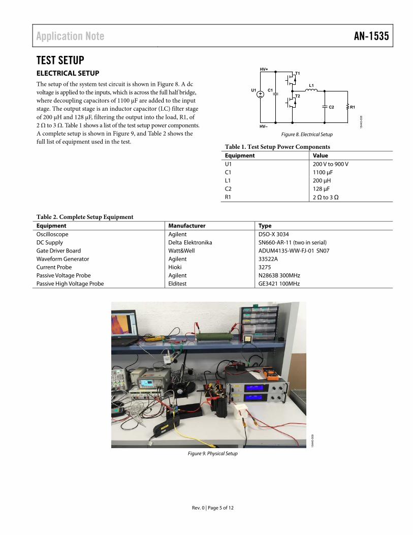
TEST SETUP ELECTRICAL SETUP The setup of the system test circuit is shown in Figure 8. A dc voltage is applied to the inputs, which is across the full half bridge, where decoupling capacitors of 1100 μF are added to the input stage. The output stage is an inductor capacitor (LC) filter stage of 200 μH and 128μF, filtering the output into the load, R1, of 2 Ω to 3 Ω. Table 1 shows a list of the test setup power components. A complete setup is shown in Figure 9, and Table 2 shows the full list of equipment used in the test.
HV+
HV–
C1U1
T1
L1
C2 R1
T2
16
440-
008
Figure 8. Electrical Setup
Table 1. Test Setup Power Components Equipment Value U1 200 V to 900 V C1 1100 μF L1 200 μH C2 128 μF R1 2 Ω to 3 Ω
Table 2. Complete Setup Equipment Equipment Manufacturer Type Oscilloscope Agilent DSO-X 3034 DC Supply Delta Elektronika SN660-AR-11 (two in serial) Gate Driver Board Watt&Well ADUM4135-WW-FJ-01 SN07 Waveform Generator Agilent 33522A Current Probe Hioki 3275 Passive Voltage Probe Agilent N2863B 300MHz Passive High Voltage Probe Elditest GE3421 100MHz
164
40-
00
9
Figure 9. Physical Setup
AN-1535 Application Note
Rev. 0 | Page 6 of 12
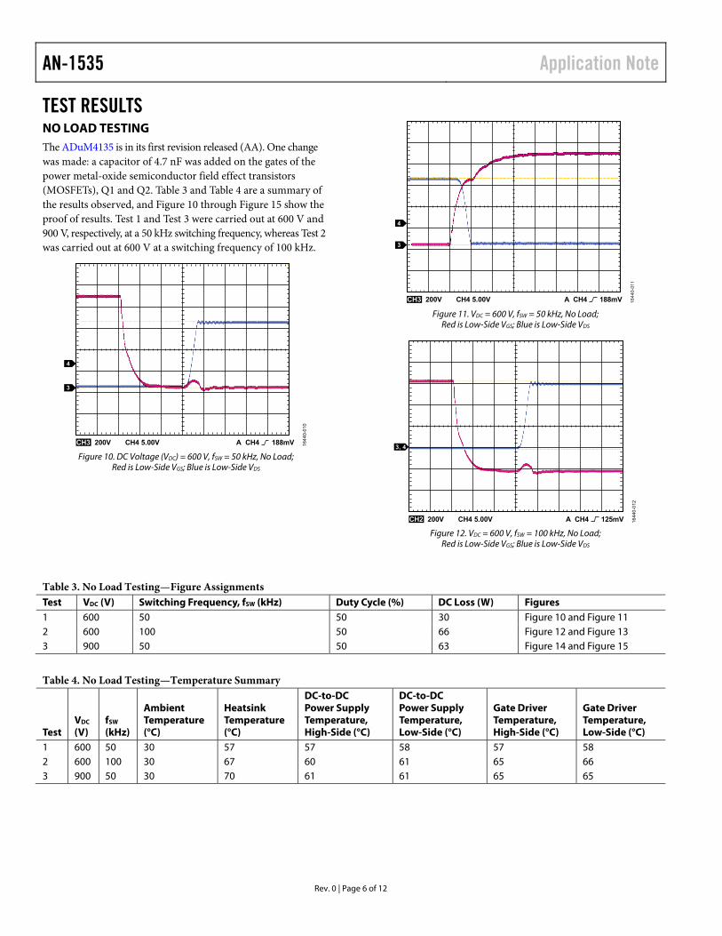
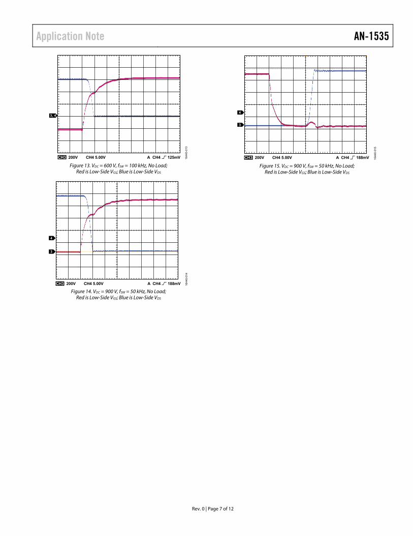
TEST RESULTS NO LOAD TESTING The ADuM4135 is in its first revision released (AA). One change was made: a capacitor of 4.7 nF was added on the gates of the power metal-oxide semiconductor field effect transistors (MOSFETs), Q1 and Q2. Table 3 and Table 4 are a summary of the results observed, and Figure 10 through Figure 15 show the proof of results. Test 1 and Test 3 were carried out at 600 V and 900 V, respectively, at a 50 kHz switching frequency, whereas Test 2 was carried out at 600 V at a switching frequency of 100 kHz.
CH3 200V CH4 5.00V A CH4 188mV
4
3
164
40-0
10
Figure 10. DC Voltage (VDC) = 600 V, fSW = 50 kHz, No Load;
Red is Low-Side VGS; Blue is Low-Side VDS
CH3 200V CH4 5.00V A CH4 188mV
4
3
164
40-0
11
Figure 11. VDC = 600 V, fSW = 50 kHz, No Load;
Red is Low-Side VGS; Blue is Low-Side VDS
3, 4
CH2 200V CH4 5.00V A CH4 125mV 164
40-0
12
Figure 12. VDC = 600 V, fSW = 100 kHz, No Load;
Red is Low-Side VGS; Blue is Low-Side VDS
Table 3. No Load Testing—Figure Assignments Test VDC (V) Switching Frequency, fSW (kHz) Duty Cycle (%) DC Loss (W) Figures 1 600 50 50 30 Figure 10 and Figure 11 2 600 100 50 66 Figure 12 and Figure 13 3 900 50 50 63 Figure 14 and Figure 15
Table 4. No Load Testing—Temperature Summary
Test VDC (V)
fSW (kHz)
Ambient Temperature (°C)
Heatsink Temperature (°C)
DC-to-DC Power Supply Temperature, High-Side (°C)
DC-to-DC Power Supply Temperature, Low-Side (°C)
Gate Driver Temperature, High-Side (°C)
Gate Driver Temperature, Low-Side (°C)
1 600 50 30 57 57 58 57 58 2 600 100 30 67 60 61 65 66 3 900 50 30 70 61 61 65 65
Application Note AN-1535
Rev. 0 | Page 7 of 12
3, 4
CH3 200V CH4 5.00V A CH4 125mV 164
40-0
13
Figure 13. VDC = 600 V, fSW = 100 kHz, No Load;
Red is Low-Side VGS; Blue is Low-Side VDS
CH3 200V CH4 5.00V A CH4 188mV
3
4
16
440-
014
Figure 14. VDC = 900 V, fSW = 50 kHz, No Load;
Red is Low-Side VGS; Blue is Low-Side VDS
CH3 200V CH4 5.00V A CH4 188mV
3
4
164
40-0
15
Figure 15. VDC = 900 V, fSW = 50 kHz, No Load;
Red is Low-Side VGS; Blue is Low-Side VDS
AN-1535 Application Note
Rev. 0 | Page 8 of 12
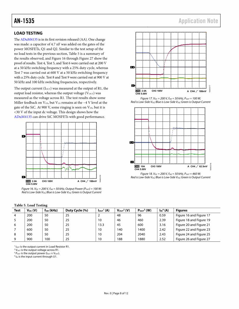
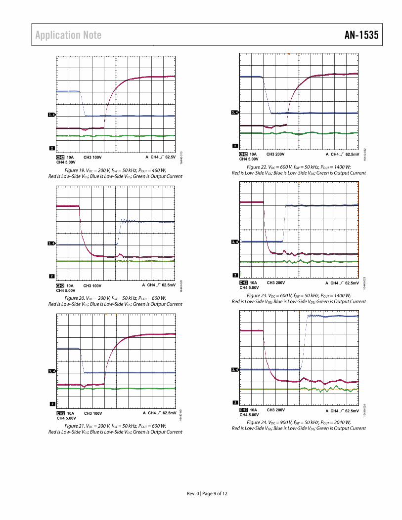
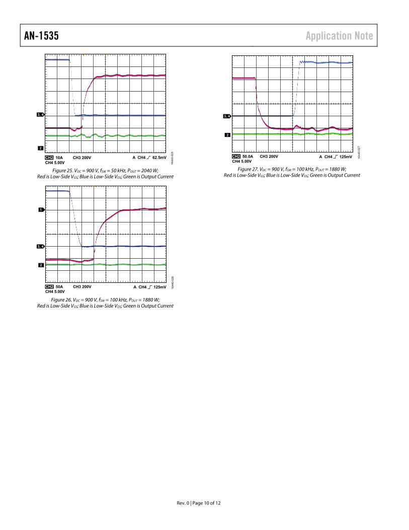
LOAD TESTING The ADuM4135 is in its first revision released (AA). One change was made: a capacitor of 4.7 nF was added on the gates of the power MOSFETs, Q1 and Q2. Similar to the test setup of the no load tests in the previous section, Table 5 is a summary of the results observed, and Figure 16 through Figure 27 show the proof of results. Test 4, Test 5, and Test 6 were carried out at 200 V at a 50 kHz switching frequency with a 25% duty cycle, whereas Test 7 was carried out at 600 V at a 50 kHz switching frequency with a 25% duty cycle. Test 8 and Test 9 were carried out at 900 V at 50 kHz and 100 kHz switching frequencies, respectively.
The output current (IOUT) was measured at the output of R1, the output load resistor, whereas the output voltage (VOUT) was measured as the voltage across R1. The test results show some Miller feedback on VGS, but VGS remains at the −4 V level at the gate of the SiC. At 900 V, some ringing is seen on VDS, but it is <30 V of the input dc voltage. This design shows how the ADuM4135 can drive SiC MOSFETs with good performance.
A CH4 188mV
4
2
164
40-
016
CH2 2.0A CH3 100VCH4 5.00V
Figure 16. VDC = 200 V, fSW = 50 kHz, Output Power (POUT) = 100 W; Red is Low-Side VGS; Blue is Low-Side VDS; Green is Output Current
2
A CH4 188mV 16
440
-01
7
CH2 2.0A CH3 100VCH4 5.00V
3, 4
Figure 17. VDC = 200 V, fSW = 50 kHz, POUT = 100 W;
Red is Low-Side VGS; Blue is Low-Side VDS; Green is Output Current
CH2 10A CH3 100VCH4 5.00V
A CH4 62.5mV
2
3, 4
16
440
-01
8
Figure 18. VDC = 200 V, fSW = 50 kHz, POUT = 460 W;
Red is Low-Side VGS; Blue is Low-Side VDS; Green is Output Current
Table 5. Load Testing Test VDC (V) fSW (kHz) Duty Cycle (%) IOUT
1 (A) VOUT2 (V) POUT
3 (W) IIN4 (A) Figures
4 200 50 25 2 48 96 0.59 Figure 16 and Figure 17 5 200 50 25 10 46 460 2.39 Figure 18 and Figure 19 6 200 50 25 13.3 45 600 3.16 Figure 20 and Figure 21 7 600 50 25 10 140 1400 2.42 Figure 22 and Figure 23 8 900 50 25 10 204 2040 2.43 Figure 24 and Figure 25 9 900 100 25 10 188 1880 2.52 Figure 26 and Figure 27 1 IOUT is the output current in Load Resistor R1. 2 VOUT is the output voltage across R1. 3 POUT is the output power (IOUT × VOUT). 4 IIN is the input current through U1.
Application Note AN-1535
Rev. 0 | Page 9 of 12
A CH4 62.5VCH2 10A CH3 100VCH4 5.00V
2
3, 4
16
44
0-0
19
Figure 19. VDC = 200 V, fSW = 50 kHz, POUT = 460 W;
Red is Low-Side VGS; Blue is Low-Side VDS; Green is Output Current
A CH4 62.5mVCH2 10A CH3 100VCH4 5.00V
2
3, 4
1644
0-0
20
Figure 20. VDC = 200 V, fSW = 50 kHz, POUT = 600 W;
Red is Low-Side VGS; Blue is Low-Side VDS; Green is Output Current
A CH4 62.5mVCH2 10A CH3 100VCH4 5.00V
2
3, 4
164
40-0
21
Figure 21. VDC = 200 V, fSW = 50 kHz, POUT = 600 W;
Red is Low-Side VGS; Blue is Low-Side VDS; Green is Output Current
A CH4 62.5mVCH2 10A CH3 200VCH4 5.00V
2
3, 4
16
44
0-0
22
Figure 22. VDC = 600 V, fSW = 50 kHz, POUT = 1400 W;
Red is Low-Side VGS; Blue is Low-Side VDS; Green is Output Current
A CH4 62.5mVCH2 10A CH3 200VCH4 5.00V
2
3, 4
16
44
0-0
23
Figure 23. VDC = 600 V, fSW = 50 kHz, POUT = 1400 W;
Red is Low-Side VGS; Blue is Low-Side VDS; Green is Output Current
A CH4 62.5mVCH2 10A CH3 200VCH4 5.00V
2
3, 4
164
40-0
24
Figure 24. VDC = 900 V, fSW = 50 kHz, POUT = 2040 W;
Red is Low-Side VGS; Blue is Low-Side VDS; Green is Output Current
AN-1535 Application Note
Rev. 0 | Page 10 of 12
A CH4 62.5mVCH2 10A CH3 200VCH4 5.00V
2
3, 4
16
44
0-0
25
Figure 25. VDC = 900 V, fSW = 50 kHz, POUT = 2040 W;
Red is Low-Side VGS; Blue is Low-Side VDS; Green is Output Current
2
1
A CH4 125mV 164
40-0
26
CH2 50A CH3 200VCH4 5.00V
3, 4
Figure 26. VDC = 900 V, fSW = 100 kHz, POUT = 1880 W;
Red is Low-Side VGS; Blue is Low-Side VDS; Green is Output Current
A CH4 125mV 164
40-0
27
CH2 50.0A CH3 200VCH4 5.00V
2
3, 4
Figure 27. VDC = 900 V, fSW = 100 kHz, POUT = 1880 W;
Red is Low-Side VGS; Blue is Low-Side VDS; Green is Output Current
Application Note AN-1535
Rev. 0 | Page 11 of 12
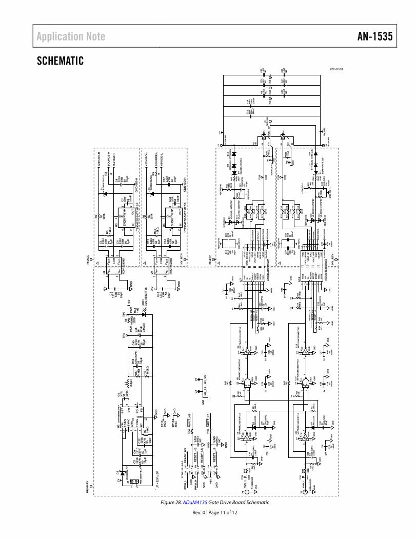
SCHEMATIC
16440-028
C48
1812
NC
C49
1812
NC
C3
1812
NC
C29
MKP
1500
220n
F
C28
MK
P15
0022
0nF
C15
1812
NC
C47
1812
NC
HV/
2H
V/2
HV/
2i
ii
C30
1812
NC
PRIM
ARY
PHA
SE
HV_
RTN
i i
C2
1210
X7R 50
10µF
C4
1210
X7R
50 1µF
C40
1210
X7R
16 22µF
C11
16 22µF
CTC
3BLE
D1
SML-
010L
TT86
R12
1kΩ
C1
1210
X7R
50 1µF
C5
X7R
50 100n
F
GN
D
GN
D
GN
D
GN
D+5V
TP10
5001
TP13
5001
GN
D
GN
D
GN
D
GN
D
V4V2
M3_
SSM
3_SS
MM
RES
ET_L
S
RES
ET_H
S
REA
DY_
HS
J3A
J3G
J3B
J3C
J3D
J3E
J3F
J3I
J3J
J3K
J3L
J3H
17
28
39
410
511
612
PWM
_L
PWM
_H
R50
REA
DY_
LS
FAUL
T_H
S
C42
006
03N
CC41
006
03N
C
C5
1210
X7R
50 10µF
C9
1210
X7R
50 1µF
C12
1210
X7R
50 10nF
R7
18kΩ
R8
180k
Ω
C10
C0G
(NP0
)50 10
pF
R5
1MΩ
L2 2.2µ
H
C6
1210
X7R
50 10µF
GN
D-IS
O-H
LT19
64ES
5-5#
TRM
PBF
U3
U2
LT86
09EM
SEaP
BF
1N58
19HW
-7-F
PM5.
08/2
/90
BLK
C7
X7R
50 10nF
+20V
-ISO
-H
R2 0
R1
R3
10kΩ
SHD
NB
YP
GND
1
OU
TIN
1Ω 1206
SOU
RC
E-H
+5V-
ISO
-H
D1
BZX
84C
20LT
1G
V OU
T+
V OU
T–
V IN
+
V IN
–
CO
M
+5V G
ND
217 6 5
4 2
3 5
U1
C14
1210
X7R 50
10µF
C16
1210
X7R
50 1µF
C21
C0G
(NP0
)10
022
0pF
C19
1210
X7R 50
10µF
C20
X7R
50 100n
F
X7R
5010
0nF
C44C
1312
10X7
R50 1µ
F
C17
1210
X7R
50 10µF
GN
D-IS
O-H
LT19
64ES
5-5#
TRM
PBF
U5
C18
X7R
50 10nF
+20V
-ISO
-L
R9 0
R6
R10
10kΩ
SHD
NB
YP
GND
1
OU
TIN
1Ω 1206
SOU
RC
E-L
+5V-
ISO
-L
D3
BZX
84C
20LT
1G
V OU
T+
V OU
T–
V IN
+
INTV
CC
TR/S
SR
TSYN
C
VIN
EN/U
V
LV
TP4
R4
5000
5000
100M
Ω12
06
TP5
+5V
LV =
12V
± 2
V
HTS
W-1
06-1
4-G
-D
D2
19 10 5 3 7 4
21
J1
28 6
11B
ST SW PG FB
GND
V IN
–
CO
M
+5V G
ND
217 6 5
4 2
3 5
U4
R51
FAUL
T_LS
PHA
SE
U7GN
D
GN
DG
ND
GN
D
C43
5V 5V5V
R22 0Ω
R40 NC
GN
D
GN
DG
ND
GN
D
C24
X7R
5010
0nF
X7R
5010
0nF
C26
50 C0G
(NP0
)47
pF
C22
50 C0G
(NP0
)10
0pF
3G
ND
R13
NC
R21
5.6k
ΩD
5FD
LL33
33
22 1
44
5V5V
5V5V
GN
D
C25
X7R
5010
0nF
5V
5V
V CC
V CC
55
REA
DY_
HS
FAU
LT_H
SR
ESET
_HS
R23 NC
C23
C0G
(NP0
)50 1n
F
X7R
5010
0nF
R15
10kΩ
R14
10kΩ
U9
MC
74VH
C1G
14D
FT1G
GN
D
GN
D
GN
D
GN
D
GN
D
C27
3
24
P1PW
M_H
TP14
R18
100Ω
R20
10kΩ
5000
GN
D
R12
4426
123
5V
V CC
5
U8
MC
74VH
C1G
14D
FT1G
U6
M74
VHC
1G13
2DFT
1G
HV_
RTN
i i
VSS1
Vi+
Vi–
REA
DYFA
ULT
RES
ETVD
D1
VSS1
BZX
84C
4V7L
T1G
D10
VS-1
0BQ
100T
RPB
F
D9
VS-1
0BQ
100T
RPB
FST
TH11
2UD
4
GN
D-IS
O-H
TP15
TP1
TP2
R26
10kΩ
R27
10kΩ
R16
10Ω
R19
10Ω
1206
1206
R38
4.7
Ω
R34
4.7
Ω12
06
1206
R24
4.7
Ω
R25
4.7
Ω12
06
1206
5000
TP16
R32
4.7
Ω
R31
4.7
Ω
1206
5000
5000
5000
SOU
RC
E-H
D14
D8
+20V
-ISO
-H
GN
D-IS
O-H
GN
D-IS
O-H G
ND
-ISO
-H
20V-
ISO
-H
5V-IS
O-H
5V-IS
O-H
GN
D-IS
O-H
+20V
-ISO
-H
D13
VS-1
0BQ
100T
RPB
F
D12
VS-1
0BQ
100T
RPB
F
GN
D-IS
O-H
+20V
-ISO
-H
+20V
-ISO
-H
C19
1210
X7R 50
10µF
C20
X7R
50 100n
F
GN
D-IS
O-L
+20V
-ISO
-H
R42
R11
1MΩ
1206
100Ω
2010
R17
10kΩ
C39
C0G
(NP0
)10
022
0pF
GN
D-IS
O-H
HV_
RTN
J6 BU
SH M
4
+20V
-ISO
-L
R35
1MΩ
1206
R47
10kΩ
STTH
112U
BZX
84C
4V7L
T1G
STTH
112U
D7
D15
D11
R46
100Ω
2010
STTH
112U
BU
SH M
4
J4
Q1 D1
Q1
J5B
USH
M4
Q2
D2S
1M
P
G1
G2 S2S1s
S2s
HV
16 15 14 13 12 11 10 9
1 2 3 4 5 6 7 8
VSS2
GAT
E_SE
NSE
VOU
T_O
NVD
D2
VOU
T_O
FFG
ND
2D
ESAT
VSS2
X7R
5010
0nF
C46
U11
GN
D
GN
DG
ND
GN
D
C45
5V 5V5V
R39 0Ω
REA
DY_
LSFA
ULT
_LS
RES
ET_L
S
R41 NC
C34
C0G
(NP0
)50 1n
F
R30
10kΩ
R29
10kΩ
U13
MC
74VH
C1G
14D
FT1G
VSS1
Vi+
Vi–
REA
DYFA
ULT
RES
ETVD
D1
VSS1
GN
D-IS
O-L
20V-
ISO
-L
5V-IS
O-L
5V-IS
O-L
GN
D-IS
O-L
16 15 14 13 12 11 10 9
1 2 3 4 5 6 7 8
VSS2
GAT
E_SE
NSE
VOU
T_O
NVD
D2
VOU
T_O
FFG
ND
2D
ESAT
VSS2
R45 NC
GN
D
GN
DG
ND
GN
D
C36
X7R
5010
0nF
X7R
5010
0nF
C38
50 C0G
(NP0
)47
pF
C33
50 C0G
(NP0
)10
0pF
3G
ND
R28
NC
R37
5.6k
ΩD
6FD
LL33
33
22 1
44
5V5V
5V5V
GN
D
C37
X7R
5010
0nF
5V
5V
V CC
V CC
55
GN
D
GN
D
GN
D
GN
D
GN
D
C35
3
24
P2PW
M_L
TP17
R33
100Ω
R36
10kΩ
5000
GN
D
R12
4426
123
5V
V CC
5
U12
MC
74VH
C1G
14D
FT1G
U10
M74
VHC
1G13
2DFT
1G
1206
R05
P215
09D
R05
P215
09D
AD
UM
4135
BRW
Z
AD
UM
4135
BRW
Z
Figure 28. ADuM4135 Gate Drive Board Schematic
AN-1535 Application Note
Rev. 0 | Page 12 of 12
CONCLUSION The ADuM4135 gate driver has the current drive capability, the correct power supply range (30 V maximum), and a strong CMTI capability of 100 kV/µs to deliver good performance when driving SiC MOSFETs.
The test results provide data showing a solution is available on the market for isolated power supply, high voltage gate drivers driving SiC.
©2018 Analog Devices, Inc. All rights reserved. Trademarks and registered trademarks are the property of their respective owners. AN16440-0-1/18(0)


![[Walter Brueggemann] 1 2 Kings a Commentary (S(Bookos.org)](https://img.pdfslide.us/doc/110x75/55cf9abd550346d033a32e47/walter-brueggemann-1-2-kings-a-commentary-sbookosorg.jpg)