Embed Size (px)
Citation preview
Non-Sequential Tool Interaction Strategiesfor Sea-of-Gates Layout Synthesis
by
Glenn David Adams
B.S. (Rice University) 1984M.S. (University of California at Berkeley) 1986
A dissertation submitted in partial satisfaction of the
requirements for the degree of
Doctor of Philosophy
in
Computer Science
in the
GRADUATE DIVISION
of the
UNIVERSITY of CALIFORNIA at BERKELEY
Committee in charge:
Professor Carlo H. Sequin, ChairProfessor A. Richard NewtonProfessor James A. Carman
1994
The dissertation of Glenn David Adams is approved:
Chair Date
Date
Date
University of California at Berkeley
1994

Non-Sequential Tool Interaction Strategies
for Sea-of-Gates Layout Synthesis
Copyright 1994
byGlenn David Adams

1
Abstract
Non-Sequential Tool Interaction Strategies for Sea-of-Gates Layout Synthesis
by
Glenn David Adams
Doctor of Philosophy in Computer Science
UNIVERSITY of CALIFORNIA at BERKELEY
Professor Carlo H. Sequin, Chair
This research focuses on strategies for managing the interaction among tools for the
automated VLSI layout synthesis of regular macro-modules, such as bit-slice datapaths. Compact
layouts for such macro-modules may be constructed by including the module’s external wiring in
the leaf cell layout. However, in most automated layout systems, module and leaf cell layouts are
performed by separate non-interacting tools. Leaf cell layouts are synthesized in advance, stored in
a library, and then customized to fit the placement and wiring of a particular module via stretching
and/or wiring personalization. This approach limits the possible customizations for a cell and the
possible layouts for a module, particularly when the use of pre-fabricated transistor arrays (as in
Sea-of-Gates) precludes the stretching of cells.
To overcome this limitation, I have developed a model for macro-module layout that
employs a high degree of tool interaction. The module floor planner decides the relative placement
and shape of function blocks that minimizes external wiring while maximizing the amount of over
the cell routing. Cell layouts are provided on demand by the SoGOLaR automatic cell generator;
their quality and feasibility are, in turn, dependent on the constraints imposed by the external wiring.
This model can easily accommodate modules with non-uniform function blocks.
Inter-tool communication is handled by maintaining a database of layouts based on a data
structure that contains both the layout state and associated metrics. The database handles all layout
requests, and maintains a history of both successful and unsuccessful synthesis attempts, all while
imposing few restrictions on tool interaction.
A separate failure handler is employed to remedy situations where the normal tool inter-
action sequence produces a floor plan that cannot be routed or no longer meets specified constraints.
The handler will undo portions of the layout and re-invoke the synthesis tools, altering their control
parameters and constraints to guide them toward a more promising solution. Repetition is prevented
2
by restricting constraint alterations and by checking the layout database for previous failed layout
attempts. Remedies are controlled by a greedy strategy that is significantly less complex than
general backtracking methods.
Carlo H. Sequin
Dissertation Chair
iii
To the memory of Professor Eugene L. Lawler and Associate Professor A. Dain Samples
iv
Contents
List of Figures vi
List of Tables viii
1 Introduction and Background 11.1 Background : : : : : : : : : : : : : : : : : : : : : : : : : : : : : : : : : : : : 3
1.1.1 Layout Styles and Layout Methods : : : : : : : : : : : : : : : : : : : : 31.1.2 Hierarchical and Task Decomposition : : : : : : : : : : : : : : : : : : : 51.1.3 Tool Interaction in Layout Systems : : : : : : : : : : : : : : : : : : : : 8
1.2 Motivation and Context : : : : : : : : : : : : : : : : : : : : : : : : : : : : : : 141.2.1 Layout by Cell Assembly : : : : : : : : : : : : : : : : : : : : : : : : : 141.2.2 Motivating Our Approach : : : : : : : : : : : : : : : : : : : : : : : : : 17
1.3 Outlining Our Approach : : : : : : : : : : : : : : : : : : : : : : : : : : : : : : 19
2 Transistor Level Layout Using Sea-of-Gates 212.1 Background and Previous Work : : : : : : : : : : : : : : : : : : : : : : : : : : 22
2.1.1 What makes good transistor layout? : : : : : : : : : : : : : : : : : : : : 222.1.2 Previous Cell Layout Systems : : : : : : : : : : : : : : : : : : : : : : : 24
2.2 SoGOLaR : : : : : : : : : : : : : : : : : : : : : : : : : : : : : : : : : : : : : 252.2.1 P/N Transistor Pairing : : : : : : : : : : : : : : : : : : : : : : : : : : : 262.2.2 Transistor Pair Placement : : : : : : : : : : : : : : : : : : : : : : : : : 272.2.3 Module Wiring : : : : : : : : : : : : : : : : : : : : : : : : : : : : : : : 33
2.3 A Comparative Study of Sea-of-Gates Template Styles : : : : : : : : : : : : : : 342.3.1 Evaluating and Selecting Template Styles : : : : : : : : : : : : : : : : : 362.3.2 Modeling Template Styles in SoGOLaR : : : : : : : : : : : : : : : : : : 382.3.3 Using SoGOLaR to Evaluate Template Styles : : : : : : : : : : : : : : : 39
2.4 Conclusions : : : : : : : : : : : : : : : : : : : : : : : : : : : : : : : : : : : : 44
3 Efficient Layout of Regular Macro-modules in Sea-of-Gates 483.1 Layout Model and Overview : : : : : : : : : : : : : : : : : : : : : : : : : : : : 523.2 Macro-Module Floor Planning : : : : : : : : : : : : : : : : : : : : : : : : : : : 54
3.2.1 Initialization : : : : : : : : : : : : : : : : : : : : : : : : : : : : : : : : 563.2.2 Initial Placement Search : : : : : : : : : : : : : : : : : : : : : : : : : : 583.2.3 Placement Adjustment : : : : : : : : : : : : : : : : : : : : : : : : : : : 62

v
3.3 Routing and Module Assembly : : : : : : : : : : : : : : : : : : : : : : : : : : 683.3.1 Global Routing : : : : : : : : : : : : : : : : : : : : : : : : : : : : : : 703.3.2 Track Assignment : : : : : : : : : : : : : : : : : : : : : : : : : : : : : 743.3.3 Module Assembly : : : : : : : : : : : : : : : : : : : : : : : : : : : : : 77
3.4 Results : : : : : : : : : : : : : : : : : : : : : : : : : : : : : : : : : : : : : : : 78
4 The Elements of Non-Sequential Tool Interaction 924.1 A Model for Inter-Tool Communications : : : : : : : : : : : : : : : : : : : : : 98
4.1.1 Overview : : : : : : : : : : : : : : : : : : : : : : : : : : : : : : : : : 984.1.2 The Layout Frame : : : : : : : : : : : : : : : : : : : : : : : : : : : : : 994.1.3 Handling Database Queries : : : : : : : : : : : : : : : : : : : : : : : : 100
4.2 A Strategy for Failure Handling : : : : : : : : : : : : : : : : : : : : : : : : : : 1024.2.1 Controlling the Application of Remedies : : : : : : : : : : : : : : : : : 1034.2.2 Handling Module Assembly Failures : : : : : : : : : : : : : : : : : : : 1054.2.3 Handling Global Routing Failures : : : : : : : : : : : : : : : : : : : : : 1104.2.4 Handling Floor Planning Failures : : : : : : : : : : : : : : : : : : : : : 115
4.3 Results : : : : : : : : : : : : : : : : : : : : : : : : : : : : : : : : : : : : : : : 116
5 Summary and Conclusions 120
Bibliography 123
vi
List of Figures
1.1 A cell and its block abstraction : : : : : : : : : : : : : : : : : : : : : : : : : : : 71.2 A standard cell layout : : : : : : : : : : : : : : : : : : : : : : : : : : : : : : : 101.3 The standard cell layout as a component of a macro-block layout : : : : : : : : : 121.4 Replicating a memory cell to form a memory block : : : : : : : : : : : : : : : : 151.5 Modeling a datapath layout in Sea-of-Gates : : : : : : : : : : : : : : : : : : : : 19
2.1 The benefits of diffusion source/drain and polysilicon gate sharing : : : : : : : : 232.2 The components of the placement cost function : : : : : : : : : : : : : : : : : : 322.3 Template styles used in comparison : : : : : : : : : : : : : : : : : : : : : : : : 362.4 Via placement in loose versus dense gate isolation template : : : : : : : : : : : : 442.5 Example layout for gate isolation template (GI) : : : : : : : : : : : : : : : : : : 462.6 Example layout for four-transistor template (LO) : : : : : : : : : : : : : : : : : 462.7 Example layout for six-transistor template (SIE) : : : : : : : : : : : : : : : : : : 47
3.1 Partitioning a two-dimensional placement problem into one-dimensional components 503.2 Floor Planning model for datapath generation showing function slices and their
connectivity : : : : : : : : : : : : : : : : : : : : : : : : : : : : : : : : : : : : 533.3 Search tree for three cell module : : : : : : : : : : : : : : : : : : : : : : : : : : 593.4 Layout model for Sea-of-Gates data cell, showing physical constraints and types of
wiring : : : : : : : : : : : : : : : : : : : : : : : : : : : : : : : : : : : : : : : 693.5 A cluster of cells and its corresponding global routing graph. : : : : : : : : : : : 713.6 Replicating a net (two instances shown) : : : : : : : : : : : : : : : : : : : : : : 743.7 An example of segment to channel assignment : : : : : : : : : : : : : : : : : : : 763.8 Floor plan for datapath example : : : : : : : : : : : : : : : : : : : : : : : : : : 833.9 Two bits of src12Cell and isCell (One row per bit) : : : : : : : : : : : : : : : : : 883.10 Two bits of src12Cell and isCell (Three rows per two bits) : : : : : : : : : : : : : 893.11 Two bits of src12Cell and isCell (Two rows per bit) : : : : : : : : : : : : : : : : 903.12 Layout of RISC style datapath (four bits shown) : : : : : : : : : : : : : : : : : : 91
4.1 Example of a layout frame. : : : : : : : : : : : : : : : : : : : : : : : : : : : : 944.2 Example of frame matching. : : : : : : : : : : : : : : : : : : : : : : : : : : : : 1014.3 Applying the cell re-routing remedy: a) Current design state with C0 as the target
cell, b) Alternate version of C0, c) Version of C0 generated if cell B1 fails tore-synthesize. : : : : : : : : : : : : : : : : : : : : : : : : : : : : : : : : : : : 107
vii
4.4 Applying the cell re-synthesis remedy: a) Current design state withC0 as the targetcell, b) Re-synthesizing bit slice containing C0, c) Restarting module assemblybeginning with C0. : : : : : : : : : : : : : : : : : : : : : : : : : : : : : : : : : 108
4.5 Adding routing space by displacing nets. : : : : : : : : : : : : : : : : : : : : : 1134.6 Alternate floor plan for RISC datapath, whose shorter external net-length is offset
by a longer internal cell net-length. : : : : : : : : : : : : : : : : : : : : : : : : 117

viii
List of Tables
2.1 Site Utilization Results : : : : : : : : : : : : : : : : : : : : : : : : : : : : : : : 412.2 Transistor Density Results : : : : : : : : : : : : : : : : : : : : : : : : : : : : : 422.3 Routability Results : : : : : : : : : : : : : : : : : : : : : : : : : : : : : : : : : 422.4 Area Results : : : : : : : : : : : : : : : : : : : : : : : : : : : : : : : : : : : : 45
3.1 Data Cell Widths (Loose GI template in bold numerals) : : : : : : : : : : : : : : 803.2 Control Cell Heights and Widths : : : : : : : : : : : : : : : : : : : : : : : : : : 813.3 Template Height Needed for Cells : : : : : : : : : : : : : : : : : : : : : : : : : 823.4 Normalized Net-length of Data Cells Module : : : : : : : : : : : : : : : : : : : 843.5 Module Net-length and its Components : : : : : : : : : : : : : : : : : : : : : : 843.6 Area results for Module : : : : : : : : : : : : : : : : : : : : : : : : : : : : : : 85

ix
AcknowledgementsThe guidance of my Dissertation Chair and Research Advisor, Professor Carlo H. Sequin,
was the greatest external factor responsible for my successfully completing this dissertation. While
all professors at UC Berkeley have the intellectual capability to successfully supervise research,
it was by observing his integrity, fairness, and strength of character that I ultimately found the
motivation to continue and finish. His inspiration has guided me when no other could.
The contributions of the other members of the Dissertation Committee were also essential.
The world-renowned expertise of Professor A. Richard Newton in design automation for VLSI has
proven invaluable, particularly in terms of orienting the research to the actual needs of VLSI
designers. Professor James A. Carman made the substantial effort needed to become sufficiently
familiar with my field to provide the insights that added clarity and precision to the dissertation.
The research described in this dissertation was supported financially by grants from
the Semiconductor Research Corporation (SRC 82-11-008), Siemens AG, Toshiba Corporation of
Japan, and the Nippon Electric Company (NEC). Also, this dissertation is based in part upon work
supported by the National Science Foundation under Infrastructure Grant Number CDA-8722788.
Portions of this dissertation contain materials that have appeared in previously published
works co-authored by Professor Carlo H. Sequin, who has given permission for said material to
appear in the dissertation. Also, portions of my research relied on use of the CODAR general area
router, written by Ping-San Tzeng.
The logistics support for carrying out this research has been supplied by the dedicated
staff of the Computer Science Division, particularly by Kathryn Crabtree, Liza Gabato, Theresa
Lessard-Smith, and Bob Miller.
From among all of the others who have provided advice and assistance over the years,
a special acknowledgement goes to Professor Eugene L. Lawler and Associate Professor A. Dain
Samples. Professor Lawler was the only member of my Qualifying Examination Committee not also
on the Dissertation Committee. Dain, while a graduate student at Berkeley, assisted me in preparing
my presentation for the qualifying exam. Sadly, in the intervening years both have departed from
x
this earth. I regret not being able to thank them personally for their efforts, and I especially regret
not having spent more time with these wonderful people. This dissertation is dedicated to their
memory.
1
Chapter 1
Introduction and Background
The field of VLSI (Very Large Scale Integration) chip design provides a rich and varied
domain in which to study the process of design engineering. Much of the interest in and effort
devoted to VLSI design is driven by the large and growing complexity of VLSI chips. A casual
observation of microprocessors and memory chips indicates that the number of transistors placed
on one VLSI chip doubles roughly every two years. This means that the number of alternatives for
implementing a given chip design, although finite, has grown well beyond the ability of a single
human designer to comprehend and the capability of current or currently proposed computers to
enumerate. In this context, the objective of computer aids for VLSI design is to assist the human
designer(s) in choosing from among the myriad of possibilities the implementation that minimizes
the desired combination of area, power and delay characteristics.
The first task in the VLSI design process is invariably to specify what chip is to be
designed. Although the initial specification language of VLSI designs is often English, Japanese,
or German, we are most interested in machine processable design representation formats, since
only these may serve as the input to computer aided design tools. Many such design representation
formats exist, these may be ordered into different levels of abstraction based on their information
content and the specific design concerns they address[1][2]. These levels may be described as
follows:
Behavioral Level This level captures the specification of how the proposed system will behave
in a manner that does not constrain the design to a particular implementation. Machine
processable specifications at this level invariably are written in a formal hardware description
language such as VHDL[3].
2
Register-Transfer Level This level describes a system’s implementation as a set of register, logic,
arithmetic, and memory blocks and the connections among them. This provides the overall
structure of the system without specifying the actual circuits to be used.
Circuit Level At this level, each transistor to be used in the design is represented explicitly as part
of either a schematic net-list or a logic level representation that can be mapped directly into
a net-list.
Symbolic Layout Level This level describes the geometric realization of the circuits on a silicon
chip. This level contains the location of the transistors and the paths taken by the intercon-
necting wires.
Mask Level At this level, the design is represented by a set of lithographic masks where each mask
corresponds to a step in the chip fabrication process. The features to be placed on the chip are
described by rectangles inscribed on each mask. A design specified at this level is considered
ready for fabrication.
The above classes are not meant to be rigidly precise. In practice, designers may use
different levels of abstraction in different parts of the design or may use information associated with
a lower level to annotate an otherwise higher level description.
From a design process point of view, the levels of abstraction described may be viewed
as a set of boundaries through which design activities may be partitioned into distinct steps in
order to manage their complexity. We refer to this partitioning strategy as task decomposition.
Each design step contains a synthesis phase in which the current design representation is refined
through optimization or the adding of structural detail to produce a representation at the same or
lower level of abstraction. Verification completes the design step, ensuring that the resultant design
representation is functionally equivalent to the initial one. Collectively, the set of steps needed to
produce a fabrication ready representation of a design is called a design path.
To reduce the amount of effort needed to complete each design step, designers will
partition a design into pieces, perform the design step on each piece separately, and later merge the
pieces. This strategy, known a hierarchical decomposition may be employed recursively, resulting
in a design representation consisting of a tree of component blocks. Hierarchical decomposition has
proven useful because both human and computer aided design steps often have complexity that is
super-linear in the size of the design. Thus, splitting the task reduces the overall effort, even when
the overhead of splitting and merging the pieces is taken into account. A further advantage is that

3
parts of a design often can be decomposed into identical sub-structures, allowing the design work
for that sub-structure to be re-used.
Although hierarchical and task decompositionreduce complexity by allowing design tasks
to proceed independently, they do not entirely eliminate the the need for feedback among design
steps or components. Components in a hierarchy must be designed such that they fit together
electrically and geometrically on a chip. Optimizing a design representation during a given task
may require information that is only fully revealed by performing subsequent tasks. Ignoring this
interaction among parts will adversely affect the quality or even the feasibility of the design.
In our research we study tool integration, this being the handling of interactions among
design step and hierarchical decompositions in the context of a framework of automated CAD tools.
The investigation focuses on tool interaction in the context of synthesizing physical layout, i.e. the
transformation of a circuit from its net-list specification to its geometric realization. The approach
we use is to explicitly incorporate knowledge about interactions across hierarchical and design task
boundaries into an automated layout system. To simplify the process of using known good layout
algorithms in our system, we have chosen to alter individual tools as little as possible. Our approach
is to use design interaction knowledge to alter the operating constraints and metrics of the individual
tools in a way that increases the performance of the overall layout system.
The rest of this chapter is devoted to motivating and outlining our approach to tool
integration. The next section begins with a brief overview of layout styles and layout synthesis
systems, focusing on issues that involve tool interaction. We then briefly describe our approach,
emphasizing those elements that contrast it from previous work. The last section contains an
overview of the layout system that embodies our approach.
1.1 Background
1.1.1 Layout Styles and Layout Methods
The term layout refers to the transformation of circuits from a structural representation
(usually a net-list) to a geometric representation suitable for fabrication. The task of layout is
determined primarily by the class of circuits to be processed and the constraints imposed by
the target VLSI manufacturing technology. This dissertation focuses on the layout of digital
circuits implemented by a set of transistors and the network of connections1 among them. These
1Each set of electrically connected nodes is a net, hence the term net-list
4
transistors and wires are to be fabricated in CMOS[4] (Complimentary Metal-Oxide Semiconductor)
technology. CMOS technology implements field-effect transistors where a voltage applied to the
gate controls the current flow between the transistor’s source and drain terminals. Electrically,
transistors in CMOS come in two types, N-type and P-type; this refers to the type of diffusion
used for the source and drain terminals. The transistors are fabricated on a planar substrate, while
the interconnect is fabricated by depositing layers of metallization on top of the transistors. The
technology targeted by our system uses two layers of metallization. Within this context, layout is
the task of embedding transistors in a plane in a way that allows the completion of interconnect with
two layers above the plane in a dense and compact manner.
As with the overall VLSI design process, there are an extremely large number of alterna-
tives for the layout of a given circuit. To reduce this complexity, designers will impose conventions
on how transistors and wires may be oriented before beginning the layout task. A set of such
conventions is called a layout style[5]. Layout style is important because it strongly influences both
the complexity of the layout task and the quality (i.e. small area, low delay and/or power) of the
resulting circuit. In the following taxonomy of layout styles, we illustrate the tradeoff between
design labor required and layout quality achieved.
At one extreme are array based approaches, such as PLAs[6][7] and Weinberger arrays[8].
Here the input circuit (expressed as a two-level Boolean logic function and a transistor net-list
respectively) is converted directly to transistor tiles. Wiring is performed implicitly by the abutting
of tiles, no explicit routing algorithm is employed. More flexible array approaches, as exemplified
by the gate matrix layout style[9], allow routing only on restricted paths so that simple algorithms
may be used. In each case, the simplicity of layout is achieved by restricting the geometry that is
produced. This restriction limits the quality of layout, particularly as the size of the input circuit
exceeds 100 transistors.
At the other extreme is the approach that allows total freedom in the placement and
orientation of both transistors and wires. As illustrated by Baltus and Allen[10], the lack of
geometric constraints on transistors leads to an extremely complex layout task that is difficult to
model in an automated layout system. Because of the complexity, the approach is reserved for
layouts where the highest quality is required and maximum effort may be expended. An example of
this is the layout of a memory cell that will be replicated in an array to form a large memory block.
Such memory blocks are a common component of digital VLSI chips[11].
Note that the tiling method used to produce such a memory block is similar to the gate
array layout style in that each method uses wiring by abutment to avoid solving a general wire
5
routing problem. The difference is that with gate arrays transistors are replicated to form a general
circuit whereas in the function block the basic tile is an entire circuit.
In between these extremes lie a set of layout styles in which transistors are constrained
to lie in rows while the wiring may take arbitrary paths over the transistors and/or between the
rows. These are referred to collectively as row-based layout styles[12]. In CMOS, by far the most
common row-based layout styles use alternating rows of P- and N- type transistors to implement
complimentary logic (also known as static CMOS) circuits[13]. Static CMOS circuits are suited
for these styles because they always contain equal numbers of P- and N- type transistors.
From a design automation point of view, this class of layout styles is very important
because the restrictions on transistor geometry are not as onerous as those in gate array styles and
yet allow for the use of automated layout tools. Individual row-based layout styles are distinguished
by the type of routing restrictions employed. These styles and the layout systems that implement
them will be discussed in a later section.
1.1.2 Hierarchical and Task Decomposition
Although the selection of a proper layout style is important, it is not the only complexity
management method used in layout synthesis. Modern VLSI digital chips are not a monolithic
collection of transistors but are a heterogeneous mixture of circuit blocks and layout styles. Con-
structing such chips involves the use of both hierarchical decomposition and task decomposition.
In this section, we illustrate how these techniques are used in layout synthesis and thereby illustrate
some basic principles common to all modern VLSI layout synthesis systems. Since our focus is
on tool interaction, we emphasize situations where interdependencies arise among layout synthesis
software tools operating on different tasks or on different levels of hierarchy.
As mentioned previously, the primary tasks in layout synthesis are the arrangement and
orientation of blocks, known as placement and the finding of paths for the interconnecting wires,
known as routing. The interdependence among these tasks arises from the manner in which they
are organized. Ideally, the placement and routing tasks would be organized as follows2:
while(Best layout not good enough)Form new trial placement;Route trial placement;
2Since all of the work described in this dissertation was implemented in the C programming language, we use a C-stylesyntax in our pseudo-code descriptions.
6
Evaluate area/delay/power of resulting layout;If (New layout better than current best layout)
Best layout = New layout;
Layout systems do not operate in this way because the complexity of routing3 is so high
that only a very few (possibly only one) trial placements can be fully routed.
Thus, in automated layout systems the placement task is a separate optimization problem
using a metric that approximates the metrics of the final layout[15]. The most common proxy for
routability is to estimate the length of all nets. One method for estimating the length of a net is to
take the half-perimeter of the bounding rectangle formed by the pins of the net. Another approach
is to model a net as the complete graph of its pins and use an appropriately weighted distance for
each edge. This measure may be supplemented by an estimate of congestion, such as measuring
the number of nets crossing a particular cut-line[16]. The key aspect of these estimation methods is
that values may be obtained without doing any routing.
Two kinds of errors may appear when a placement based on wiring estimates is sub-
sequently routed. First, because the location of wires is not specified during placement, wires
may become congested locally and exceed the amount of space available at a particular location.
Secondly, the final wiring length of a particular net may exceed its estimate. This becomes critical
when nets have bounds placed on their length derived from signal delay bounds.
The effect of the errors is that the wiring of the chip or block may fail to complete without
modifying its placement. This issue is complicated by the fact that the original placement tool uses
a proxy rather than an explicit model of the routing. We will discuss methods of addressing this
issue in the detailed exposition of layout systems in the next section.
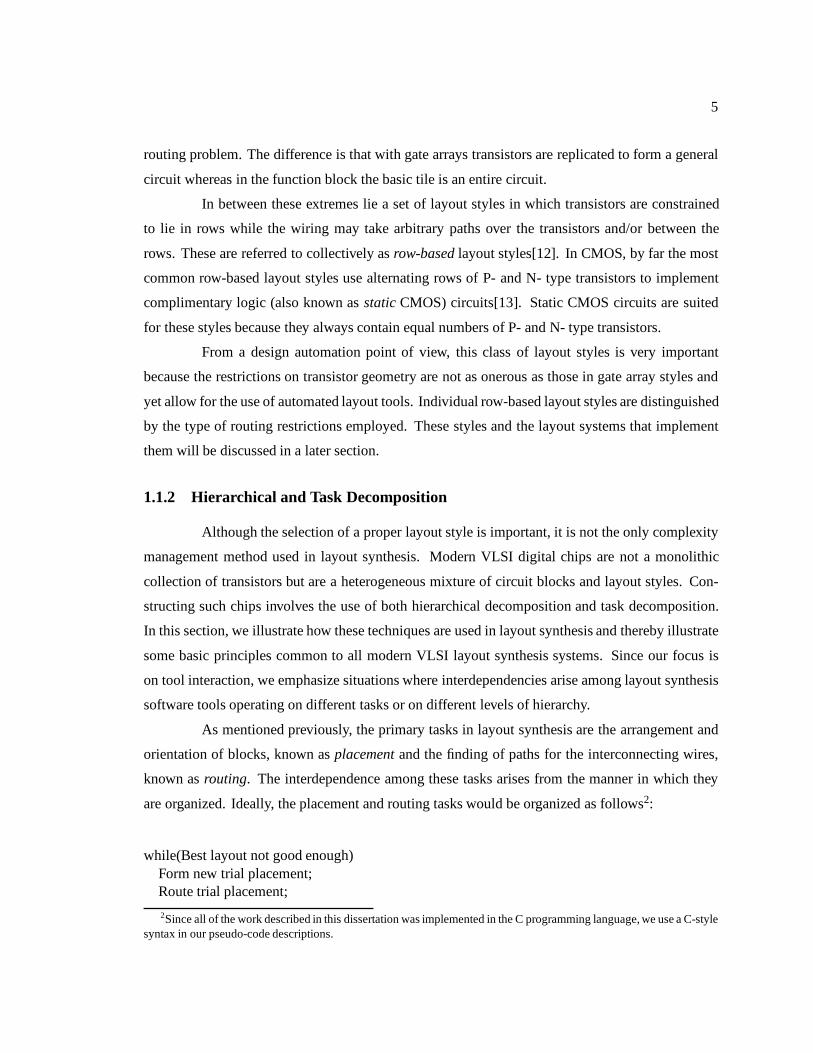
Hierarchical decomposition in layout synthesis is accomplished by augmenting net-lists
with an abstraction mechanism called a block. Previously, we described a circuit net-list as a set of
transistors and a set of nets, where each net is a list of transistor pins to be connected. The block
mechanism encapsulates and abstracts the net-list of the objects (blocks or transistors) within it.
Nets that must connect to nodes outside the block are abstracted by adding a pin for that net to the
block. On the outside of the block, a connection made to a pin on the block represents a connection
to the pins of the sub-net inside the block. Applying this mechanism recursively results in a tree
3Both placement and routing are NP hard for at least one dimension and at least two layers of wiring[14].
7
Vdd
Vss
N-Diffusion
P-Diffusion
Polysilicon
Metal 1
Contacts
B
A Out OutA
B
Vss
Vdd Vdd
Vss
Figure 1.1: A cell and its block abstraction
of circuit blocks with transistors being the leaf elements of the tree. Figure 1.1 illustrates the block
abstraction mechanism as exemplified by a static CMOS 2-input NAND gate.
Many VLSI layout systems use different synthesis tools on different levels of the net-list
hierarchy[17]. Typically, the boundary is at the transistor-level where the layout of circuits at the
transistor level is handled by a different tool from the block-level synthesis tool4. This approach
allows the macro-block layout tool to operate on the block abstraction of the circuit, freeing it from
the details of implementing the chosen layout style. In turn, the automatic cell layout tools use
specialized algorithms geared to the known interconnection pattern of transistors (gate, source, and
drain) and the particular layout style.
Because both the macro-block and cell layout tools are performing the same function,
their operation is interdependent. The focal point of this interdependence is the geometric interface
of the cell, specifically its shape and pin positions. The placement and routing of the cells that
form a macro-block is dependent on the cell’s shape, size and pin positions, since ultimate the sub-
blocks must fit together efficiently without overlap. Thus, the top level tool must have a reasonable
approximation of the layout of the sub-blocks. However, performing the layout of cells first may
overconstrain the operation of the macro-block level tool. A cell layout that is locally optimal may
not be globally optimal when it is combined with the other cells of the macro-block.
A similar interaction occurs in those layout systems that treat the net-list as immutable and
exploit its structure to simplify the layout task. For example the a typical processor datapath consists
of a set of function blocks to be placed side by side where each block is a one- or two-dimensional
array of circuit cells. By performing the layout of the function blocks first, the layout synthesis of
4Sc2D[18] is the notable exception to this
8
the top level can be reduced from a two-dimensional task to a one-dimensional one. The details of
how these module assemblers operate will be discussed in the next section.
The interdependencies associated with hierarchical interaction at the tool level also appear
when examining the behavior of individual layout algorithms. For instance, many layout systems
create hierarchy in the course of layout through the use of algorithms that employ the “divide and
conquer” paradigm. An important example is the mincut placement algorithm in which blocks are
placed into either two[19] or four[20] roughly equal regions so as to minimize the number of nets
that cross the region boundary. At each step the algorithm must also balance the relative sizes of the
sub-regions along with the sizes of the blocks. This step is employed recursively until each block
occupies its own region. Similar algorithms[21][22] exist for wire routing as well.
Interdependencies across the boundaries created by these algorithms account in part for
the sub-optimal performance of these algorithms on some problems and for the lack of provable
guarantees regarding the performance of any hierarchical layout algorithm. The scope of this
dissertation extends beyond the behavior of a single algorithm or group of algorithms, and we do
not purport to resolve interdependencies within an algorithm to improve its performance specifically.
We include individual algorithms in this discussion because many existing layout systems attempt
to handle tool interaction by improving on the basic algorithms outlined above. These strategies
and the systems that use them are the subject of the next section.
1.1.3 Tool Interaction in Layout Systems
The above section presented an abstraction of techniques that are applied in a variety of
layout systems. To fully understand these techniques and to provide a context for our research, it is
necessary to discuss specific systems and contexts. Practical layout systems are a combination of
layout styles and methods of task and hierarchical decomposition. The number of combinations and
thus the number and diversity of layout systems is quite large. Rather than simply enumerate these
combinations, the discussion focuses on how layout systems handle the interdependencies among
their component tools. In particular, we discuss those instances where a tool has been modified
or created to handle a particular interdependency. However, many existing layout systems do not
have an explicit strategy for handling tool interaction. In these cases we reach our conclusions by
studying the task partitioning in these systems and its implications for the component tools.

9
Standard Cell Layout
We begin the discussion with layout systems built for the standard cell[12] layout style.
The standard cell layout style is an example of a row-based layout style, in which static CMOS
circuits are implemented by rows of P- and N- transistors. Each row contains transistors of one
type placed horizontally adjacent to one another. The P- and N- transistor rows are then stacked
vertically, with transistors that use the same gate input net vertically aligned. To create the input
net-list for this layout style, a large circuit block is decomposed into a collection of relatively simple
logic functions which may be implemented using one or at most two rows. The macro-block is
produced by abutting the cells to form one or more long rows. To make this abutment feasible, the
internal wiring for each cell is routed within the boundaries of the row of transistors as much as
possible. Usually, the power supply rails run parallel to the transistor rows to form this boundary.
The external wiring among cells is routed in the regions between rows. These regions are called
channels and the routing problem where pins appear on two sides of the routing region is called the
channel routing problem[23]. Part of a cell’s internal wiring includes the wiring for connections
that extend outside the cell. This is done by routing wires from the interior of the cell to pins on the
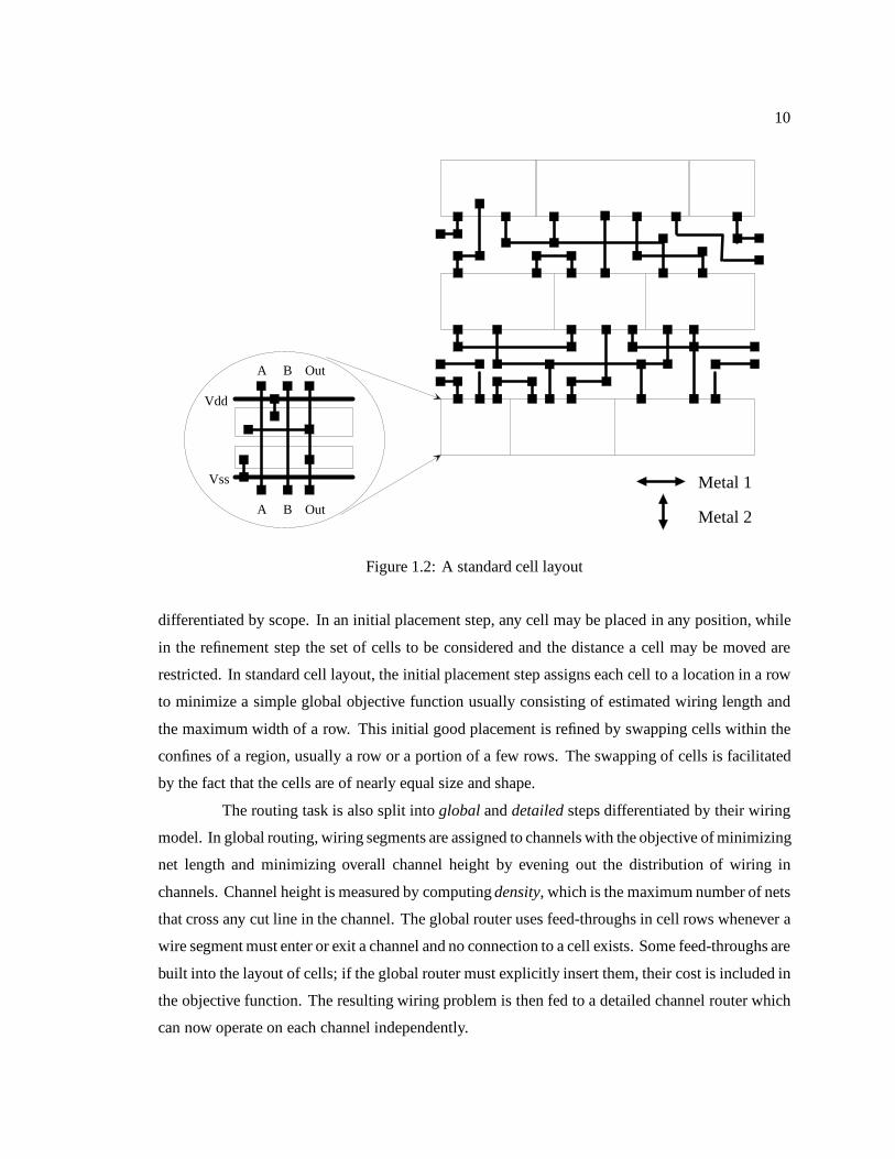
two sides perpendicular to the transistor rows. Figure1.2 illustrates the typical cell and macro-block
arrangements for this type of layout.
A key feature of this system is that the macro-block and cell layouts are performed by
entirely different tools with very little interaction. The number of different types of elementary
circuits needed to form large digital macro-blocks is relatively small, usually on the order of 100
types of circuits. Because each cell is small, of standard shape, and has no external wiring going
through it, there is very little to be gained by customizing the layout of every cell instance. Thus,
the layout of each gate is done once in advance for each kind of cell, either manually or with an
automated tool, and every instance of that cell uses the same layout. The layouts are stored in a
library along with the block abstraction for use by the macro-block layout tool.
This approach minimizes the interaction between the different layout tools but complicates
the layout problem at the block level. Since a macro-block may contain tens or even hundreds of
thousands of these elementary logic cells, the placement and routing tasks require automated
methods. Because of this complexity, the cost of producing a placement that subsequently cannot
be routed is very high.
One method employed to reduce this cost is to sub-divide the routing and placement tasks.
For instance, the placement task is often divided into initial and refinement steps where the steps are
10
Metal 1
Metal 2
Vdd
Vss
A B Out
A B Out
Figure 1.2: A standard cell layout
differentiated by scope. In an initial placement step, any cell may be placed in any position, while
in the refinement step the set of cells to be considered and the distance a cell may be moved are
restricted. In standard cell layout, the initial placement step assigns each cell to a location in a row
to minimize a simple global objective function usually consisting of estimated wiring length and
the maximum width of a row. This initial good placement is refined by swapping cells within the
confines of a region, usually a row or a portion of a few rows. The swapping of cells is facilitated
by the fact that the cells are of nearly equal size and shape.
The routing task is also split into global and detailed steps differentiated by their wiring
model. In global routing, wiring segments are assigned to channels with the objective of minimizing
net length and minimizing overall channel height by evening out the distribution of wiring in
channels. Channel height is measured by computing density, which is the maximum number of nets
that cross any cut line in the channel. The global router uses feed-throughs in cell rows whenever a
wire segment must enter or exit a channel and no connection to a cell exists. Some feed-throughs are
built into the layout of cells; if the global router must explicitly insert them, their cost is included in
the objective function. The resulting wiring problem is then fed to a detailed channel router which
can now operate on each channel independently.
11
Task sub-division provides the flexibility to use more than one cost function or wiring
model in a given layout task. Because this advantage alone is not enough to overcome the problems
caused by doing routing after placement, some row-based layout systems[24] integrate the functions
of placement refinement and global routing. A simple method of accomplishing this objective is to
place the tasks into an iteration loop beginning with a global routing of the initial placement. This
allows the placement refinement step to use the more sophisticated global routing cost function,
using wire segment lengths instead of half-perimeter estimates and taking into account channel
density and number of feed-throughs.
Since the movement of blocks changes the global routing of both the nets attached to the
displaced blocks and the nets that are in the vicinity of the displacements, each block move triggers a
substantial recomputation of the global routing. Furthermore, these changes may affect the utility of
further moves, rendering inaccurate any attempt to compute the net-length and congestion resulting
after several such moves. These added complexities mean that this method is used only for short
moves and therefore can achieve only incremental improvement of the quality of layout.
These limitations have provided the motivation for developing systems that attempt to
perform placement and global routing simultaneously. Most of these systems use a top-down
partitioning algorithm based on either a quadrisection[20][25] or a 2xN grid structure[26]. Some
form of global routing is then used to assign nets to paths among the rooms in the partition; the
aforementioned grid structures have been chosen because efficient algorithms exist for performing
this assignment. The combined partitioning/global routing procedure is then applied recursively.
This allows the global routing paths at one level to influence the partitioning of blocks at the next
lower level.
The primary drawback to these algorithms is that they do not eliminate interdependencies
at hierarchical boundaries. Instead, the effects of interdependencies are manifested in the internal
operation of the algorithm. For instance, at the top-level, blocks whose proper placement is near the
middle of the target region may be arbitrarily assigned to one side or the other of the first cut-line
in order to minimize the number of nets crossing said line. Although the subsequent use of global
routing information can compensate for these effects at lower levels, it cannot completely undo them.
This has led to the development of more sophisticated approaches to partitioning[27][28] in which
blocks partitioned at one level may actually cross over previously formed cut-lines. Unfortunately,
there is no way to directly integrate global routing with this particular partitioning method.
12
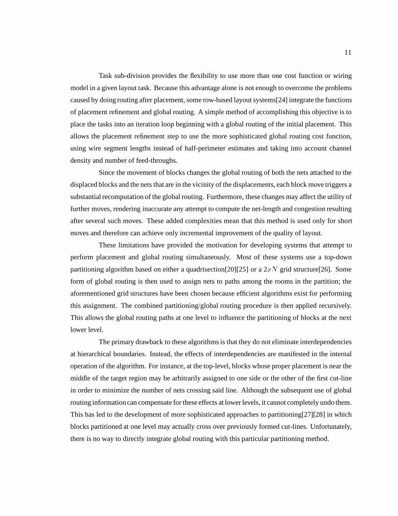
Figure 1.3: The standard cell layout as a component of a macro-block layout
Macro-block Layout
A similar approach to minimizing tool interaction can be seen in the placement and
routing of macro-blocks. The macro-block layout problem is more general than row-based layout
in that blocks may possess different sizes and aspect ratios, may have pins on all four sides and
may assume arbitrary relative positions (i.e. blocks are not fitted into rows). Wiring among the
macro-blocks may be routed in channels between blocks or may be allowed to pass through the
blocks on metallization layers not used by the block’s internal wiring. While restricting the wiring
to channels may be less area and net-length efficient, it does permit the use of the channel routers
already developed for row-based layout systems. Allowing wires to pass over the interior of blocks
begets a more complex area routing[29] problem. By supporting a more general placement and
wiring model, the macro-block level tool is able to accept blocks produced by any of the layout
styles mentioned above, including macro-blocks produced by a row-based layout system. This
principle is illustrated in Figure 1.3.
13
At one time, macro-block placement was considered a special case of the floor planning
problem, in which individual blocks are allowed to vary their aspect ratio and pin positions. Early
approaches to floor planning, such as Mason[30], combine a top-down partitioning of blocks with
a bottom-up grouping of blocks into floor plan templates. In this context, a floor plan template is
simply the sub-division of a rectangle into two or more rectangles; each of the sub-divisions is called
a room. Since the number of topologically distinct floor plan templates is an exponential function
of the number of rooms allowed[31], templates were typically limited to at most four or five rooms.
Templates with four or fewer rooms are known as slicing structures[32]; using only these templates
simplifies the problem of choosing an ordering for routing the channels between rooms.
The lack of uniformity in both the input blocks and their relative placements makes the
interdependencies among levels of hierarchy even more manifest in floor planners than in row-based
layout. For instance, in Mason blocks are partitioned according to a cost function that considers only
the aggregate size of each partition and the wiring cost among the partitions. This approach may
therefore assign a group of blocks that fit well together geometrically into different partitions. As
the partitions are further sub-divided, this may result in a partition being occupied by blocks whose
shapes do not fit well together. This is especially true when individual blocks are “hard” (i.e. of
fixed shape) as in the macro-block placement problem. Grouping blocks together in a “bottom-up”
fashion with a clustering metric[33] can often find these locally good groups of blocks. However,
there is no guarantee that at the top-level the groups will fit together to meet global objectives or
constraints.
The similarity of this type of interdependencies to those found in row-based layout has
driven the development of analogous approaches to simultaneous placement and global routing.
Hierarchical systems were developed in the context of both floor planning[31] and macro-block
place and route[34]. Several such tools[35][36] explicitly attempt to combine top-down partitioning
with bottom-up clustering.
More recent efforts have integrated sub-tasks more tightly by performing them on a
common data structure. For example, in the CODAR area router[37], a grid of capacity constraints
is made a part of the underlying wiring grid. This allows the tool to change the path of wire
segments (a process known as rip-up and reroute) on a global scale if necessary. Further work in
macro-block[38] and row-based[39] place and route focuses on developing a single data structure
that combines global routing with space allocation.
14
1.2 Motivation and Context
As seen in the previous section, many layout systems address tool interdependency issues
through the development and improvement of specific algorithms. Wherever possible, the interfaces
between tools are made as simple as possible, even at the expense of making the tools at each end
of the interface more complicated. In particular, the tools that perform layout at the macro-block
level are expected to use the modules supplied to them as is, with little attempt made at customizing
the input blocks. Rather than graft our approach onto a layout system where tool interaction is
minimized, we demonstrate our ideas in the context of creating high-performance macro-modules
from customized cells.
In this section, we describe this layout context and contrast it to the methods presented
earlier. We then present a brief description of our system for automated layout in this context in
order to contrast it with existing approaches and to motivate the more detailed description given in
the next section.
1.2.1 Layout by Cell Assembly
Our research focuses on the layout of macro-modules whose circuitry has a regular
structure. An important and illustrative class of macro-blocks with this structure are datapaths with
a bit-slice organization[40]. A bit-slice datapath consists of a number of function blocks, such as
memory cells, register files, shifters, ALUs and the like, where each of the function blocks operates
on a number of bits in parallel. To process bits in parallel, each function block consists of an array
of similar cells. The wires among the cells in a function block form a regular pattern of signal
propagation. Typical patterns within a function block would include a control signal that connects
a separate control cell to the same input in each of the function block’s cells, or a connection to
propagate the output of one cell to the input of an adjacent one. This latter type of connection
would be found in counters or shift register blocks, for example. A bit-slice consists of a row of
interconnected cells where each cell is part of a different function block. Collectively, these cells
perform all needed processing for one data bit. The wiring that propagates the data in each bit slice
may use point-to-point connections or shared data busses.
As seen in the above example, not all cells in a regular a macro-module need to be
identical, nor must all wires follow a rigid pattern. However, the degree to which a module is
regular greatly influences the utility and complexity of any layout technique designed specifically
to exploit a module’s regular structure. When a block consists of an array of like cell instances,

15
Vdd
Vss
WA WA_b
WA WA_b
BIT
BIT_b
BIT
BIT_b
WB WB_b
WB WB_b
Bit 2
Bit 1
Bit 0
Word 0Word 1
Word 2
Figure 1.4: Replicating a memory cell to form a memory block
the cell is laid out only once and the result is replicated to create the block. Because the wiring
has a regular structure as well, the cell layout contains not only its own wiring but also the external
wiring that must pass through it in order to wire the block. This allows the entire block to be routed
by cell abutment without any external wiring channels. An example of how a memory cell can be
replicated to form a block of memory is given in Figure 1.4.
The layout process used for regular structured macro-blocks is called cell assembly. The
cell assembly may be divided into the following tasks:
1. Selecting a floor plan for the macro-block. This includes finding an arrangement of cells that
produces a regular wiring pattern and finding a suitable aspect ratio (ratio of width to height)
for the block.
2. Translating the wiring pattern and aspect ratio of the block to pin location and aspect ratio
constraints for each cell.
3. Performing the layout of each cell.
16
4. Producing the layout of the block by replicating the layout of its constituent cell(s).
For a block with a single type of cell, the first two steps of this process are usually
straightforward. If the macro-block has several types of cells as in the datapath example, the floor
planning task is expanded to include determining the relative placement of the function blocks.
Also, the floor planning task must match the pitch of each of the function blocks in a bit slice. For
instance, if the register file uses a memory cell that processes a single bit and the ALU processes
two bits in one cell, then the ALU cell must be twice the height of the memory cell for them to
match when placed side by side.
Compared to a general layout system, the use of a specialized layout approach for regular
structure macro-blocks provides several advantages. First, this layout approach can fit blocks
together to produce results of very high quality by directly minimizing both the length of external
wires and the area used by the block. Cell assembly also preserves the circuit hierarchy created
by the designer, this can simplify simulation and verification tasks. However, this approach is very
labor intensive relative to fully automated methods because a human designer must devise both the
module floor plan and a custom layout for each cell. In many designs, this labor cost is high enough
to offset the advantage of higher quality. This has led to efforts to automate cell assembly.
Much of the effort in automating cell assembly has consisted of the development of a
language for the input of module floor plans. This language is then translated to an internal represen-
tation that guides the tiling of a structured block. Such an input language may be procedural[41][42]
or graphical[43] in form, and all include the ability to personalize the wiring of a particular cell in
the array. This approach reduces design cost by allowing the re-use of expensive cell layouts. A
cell layout may be stored in a library, and then customized to fit a particular floor plan by stretching
and/or wiring personalization. These features are implemented in part by giving the tiling tool the
ability to stretch cell layouts and in particular external pin positions. Some tiling tools[44][45] also
have the ability to implement some module wiring via river routing.
Even with these improvements, cell assemblers are significantly more labor intensive
compared to fully automated macro-block or row-based layout systems. Floor planning for regular
macro-blocks is still largely a manual task, and pre-formed cell layouts are limited in the degree to
which they can be customized for a particular floor plan. Thus, for a given design the number of
alternative floor plans that can be explored is very limited.
17
1.2.2 Motivating Our Approach
We have chosen to implement and test our research ideas by developing a fully automated
layout system for regular structured macro-blocks. Our system overcomes the limitations of cell
assemblers by implementing a general and flexible model for structured macro-blocks. In our
system, macro-blocks may contain function slices with more than one type of cell and function
slices that process different number of bits. The wiring model allows busses that must jog vertically
to do so inside a cell wherever possible. Also, our system will selectively dissolve the boundaries
between adjacent control cells and function slices if removing said boundaries would reduce area
and/or wiring length without inordinately increasing wiring density.
To implement this model, the floor planner in our system must decide not only the relative
placement of function blocks that minimizes the wiring among them but also the alignment and
aspect ratio for each block that maximizes the amount of wiring that can be routed by abutment.
Because the external wiring passes through each cell, the floor planner must also ensure that the
external wiring load through each cell is distributed such that its layout can be completed.
The floor planner makes use of the SoGOLaR[46] cell generator to provide customized
cell layouts at the transistor level to match particular aspect and pin position constraints. The
circuitry may be specified either as a list of Boolean expressions where each expression specifies
a multi-level AOI tree, or alternatively as a schematic level net-list. SoGOLaR uses a flexible
placement strategy where transistors are first grouped into P/N pairs and then placed on a symbolic
grid using a cost function that takes into account both diffusion sharing and wiring length. This
approach allows us to emphasize a particular objective (i.e. maximum bus capacity or minimum
cell width) by changing relative weights in the placement cost function.
The aforementioned individual tool capabilities are necessary but not sufficient to meet
the requirements of our system. For the floor planner to choose a suitable arrangement of function
blocks and wiring, it must have accurate information regarding the quality of each cell layout as
well as information on the feasibility of proposed wiring patterns. In turn, the quality and feasibility
of a particular cell layout is highly dependent on the constraints imposed by the external wiring.
Because existing systems use an “arm’s length” interface between the macro-block and transistor
level, they do not support the two-way interaction needed to resolve this interdependency.
In a semi-automatic cell assembler, the human designer can use his/her design knowledge
and experience to provide a substitute for this interaction. However, in an automated system the
human designer is limited in the control that he/she can exert over the floor planning and routing
18
algorithms to modify their behavior in the presence of new information. In many such systems, the
designer’s role is limited to aborting a certain routine and/or restarting another with some different
control parameters. Also, the tools do not communicate specific knowledge needed to evaluate the
viability of design alternatives. Without an exchange of data about partial results and constraints,
it is difficult to change the behavior of individual routines in a manner that produces better results.
There is no guarantee that simply running the algorithms again will produce a better solution.
To achieve the degree of tool interaction required, our system is organized as a collection
of cooperating tools with a separate tool to handle design interaction known as the design mediator.
In the initial floor planning stage, the design mediator handles the interaction between floor planner
and cell generator in order to select the best aspect ratio for the floor plan as well as the best cell
implementations for a particular arrangement of function blocks. Subsequently, if it is determined
that the chosen floor plan cannot be routed or the result no longer meets a specified constraint,
the design mediator will intervene to find another way to complete the layout. This intervention
involves altering the control parameters and constraints given to the synthesis tools to guide them
toward a more promising solution.
To provide the coupling and information exchange needed to sustain this tool interaction,
the components in our system communicate via a database that uses a structure called a layout
frame. This layout frame contains the constraints and cost function weights to be used when
invoking a layout tool as well as the results of an attempted implementation. The design mediator
uses this database both to issue layout requests to the synthesis tools and to maintain a history
of both successful and unsuccessful synthesis attempts. This historical data aids the mediator in
determining the viability of different failure recovery options.
Our system is designed for the row-based layout of static CMOS circuits. As seen in
our discussion of existing layout systems, this layout style is suitable for rapid low-cost VLSI
design. Also, by implementing only static CMOS circuits we avoid the transistor level layout issues
associated with supporting automated layout of one or several dynamic circuit design styles. Since
these details are manifest exclusively in the layouts of cells, they are peripheral to our focus on tool
interdependency problems.
Although our research ideas are applicable to any row-based layout style, we have chosen
to demonstrate and test our system using the Sea-of-Gates layout style. In the Sea-of-Gates layout
style, the transistors are pre-fabricated in a continuous tiled array, with circuits being formed by
programming the interconnect among the transistors. The interconnect among transistors in this
array uses at least two layers of metal. This layout style differs from previous gate array layout
19
Controlcells
0
1
2
3Data cell Data cell Data cell Data cell
Shifter ALU Mux
Function slices
BitSlices
Register file
BussesN-Diff.
P-Diff.Vdd
Vss
Metal 1
Metal 2
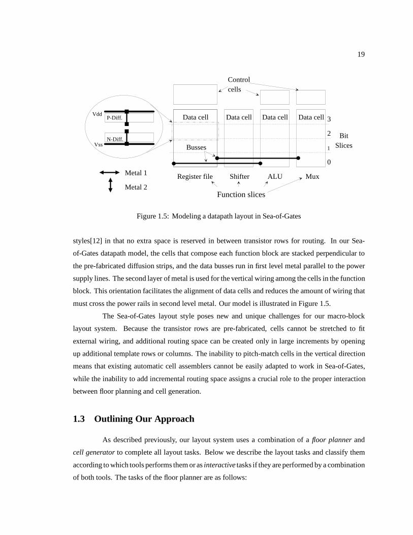
Figure 1.5: Modeling a datapath layout in Sea-of-Gates
styles[12] in that no extra space is reserved in between transistor rows for routing. In our Sea-
of-Gates datapath model, the cells that compose each function block are stacked perpendicular to
the pre-fabricated diffusion strips, and the data busses run in first level metal parallel to the power
supply lines. The second layer of metal is used for the vertical wiring among the cells in the function
block. This orientation facilitates the alignment of data cells and reduces the amount of wiring that
must cross the power rails in second level metal. Our model is illustrated in Figure 1.5.
The Sea-of-Gates layout style poses new and unique challenges for our macro-block
layout system. Because the transistor rows are pre-fabricated, cells cannot be stretched to fit
external wiring, and additional routing space can be created only in large increments by opening
up additional template rows or columns. The inability to pitch-match cells in the vertical direction
means that existing automatic cell assemblers cannot be easily adapted to work in Sea-of-Gates,
while the inability to add incremental routing space assigns a crucial role to the proper interaction
between floor planning and cell generation.
1.3 Outlining Our Approach
As described previously, our layout system uses a combination of a floor planner and
cell generator to complete all layout tasks. Below we describe the layout tasks and classify them
according to which tools performs them or as interactive tasks if they are performed by a combination
of both tools. The tasks of the floor planner are as follows:
20
� Determine relative placement of sub-blocks in macro-block.
� Compute all layout metrics for a given arrangement of cells into a macro-block.
The tasks of the cell generator is to produce (if feasible) the placement and routing of the
transistors that form a particular cell. The generator must be able to handle the external specification
of external pin positions and reserved tracks for through the cell wiring.
The tasks requiring interaction between the cell generator and floor planner include:
� Choosing the module aspect ratio. The cell generator determines the feasibility of the cells
needed to assemble the module into a particular shape, while the floor planner must compute
the layout cost for each configuration and then select the best one.
� Routing the external wiring for the module. The floor planner must coordinate the pin
positions and track assignments for a given net in order for the net to pass through and
connect to the proper cells. The cell generator must provide a sufficient number of available
wiring tracks and perform the final connections from the internal cell wiring to the external
nets.
The role of the mediator component of our system is to support the execution of the
interactive tasks. It does this by providing the following capabilities:
� Maintain and provide access to the database of past and current layout requests.
� Characterize the failures that may arise during an interactive task to the extent necessary to
select one of several possible corrective measures.
� Implement the chosen corrective measure. This may involve restarting either of the layout
tools with new objectives and/or constraints.
The design and operation of the cell generator SoGOLaR and the floor planner are
discussed in Chapters 2 and 3 respectively. Because the mediator only intervenes in the layout
process, in these chapters we describe the operation of these tools under the assumption that no
tool failures occur. This allows us to focus on the tasks that these tools perform by themselves.
Chapter 4 describes the elements necessary to support the layout tools when they perform interactive
tasks. After describing the tool communication database, we present a detailed description of the
intervention strategy and corrective actions available for each interacting task.
21
Chapter 2
Transistor Level Layout Using
Sea-of-Gates
The term transistor level layout refers to the process of transforming a circuit network of
transistors, called a cell, into a physical realization. The layout of a cell differs from block layout
in that we must explicitly model the geometry of transistors in order to get satisfactory results.
The need to incorporate transistor features means that performing transistor level layout
manually is a difficult and labor intensive task. In fact, traditional design approaches for layout
are driven, at least partially, by the need to minimize the amount of cell layout that must be done.
This is done by attempting to re-use the same cell layouts in as many places as possible. In
traditional datapath design, this is done by exploiting the regularity present in the circuit net-list.
In non-datapath oriented “irregular” circuit designs, the design is partitioned into groups that can
implemented by a small fixed set of cells, often called a cell library. Often, only one layout is done
for each cell in the library, and that layout is re-used for each instance of the cell in the design.
There are many tools available for the automatic generation of leaf cells for cell libraries,
these are designed to augment an existing chip layout approach. Our leaf cell generator differs
substantially from previous work in that it is an integral part of an automatic datapath generation
tool. Specifically, this means that our cell generator must be able to generate cells on demand to a
set of specifications. Our tool must be able to handle externally imposed constraints on the shape
of cells as well as on the location of wiring. Also, we cannot impose any restrictions on the kind or
size of transistor circuits our tool will accept. These requirements exceed the capabilities of those
automatic layout generators that are designed to produce cells for fixed layout libraries.

22
Although the fixed location and size of transistors in the Sea-of-Gates layout style removes
the need for transistor sizing algorithms and reduces the need for layout compaction, the use of this
layout style adds challenge to the problem in two ways. First, it makes achieving the flexibility
needed for datapath generation more difficult. Secondly, the features of Sea-of-Gates geometries
change the formulation of the layout problem enough to ensure that conventional transistor layout
methods cannot be applied directly. Collectively, these requirements have motivated us to create a
unique approach to transistor level layout. We call the result SoGOLaR, which stands for Sea-of-
Gates Optimized Layout and Routing.
Another challenge arising from the use of the Sea-of-Gates layout style is that there is
no single universally accepted way to arrange transistors into Sea-of-Gates templates. Thus, we
have incorporated into our generator the capability to produce layout for a variety of Sea-of-Gates
templates. This is done by using a parametric model to capture those attributes of Sea-of-Gates
templates relevant to transistor placement and routing into a parametric model. Besides added
flexibility, this gives us the ability to study different templates from a point of view of efficient cell
generation. This study and the parametric model are discussed in the last section of this chapter.
2.1 Background and Previous Work
As mentioned previously, there exist a tremendous variety of tools that may be called
transistor level layout generators. We do not attempt a comprehensive survey of these tools here;
the discussion below is limited to those approaches and principles that are applicable to the Sea-of-
Gates layout style. Of particular interest are those tools that are capable of transforming a net-list
representation of a circuit into a row-based layout of transistors. This excludes those tools that tile
transistors into regular arrays (such as the PLAs and Weinberger arrays mentioned in Chapter 1),
or whose layout style utilizes multiple strips of diffusion per row (e.g. gate matrix). However, this
still leaves a wide variety of tools, some of which have contributed ideas to SoGOLaR. Before
discussing these contributions, we attempt to place them in perspective by describing in greater
detail the metrics by which row-based transistor layouts are judged.
2.1.1 What makes good transistor layout?
Metrics for cell layout are derived from the general metrics for good layout (i.e. small area,
low delay and/or power) by taking into account the geometric particulars of arranging transistors
23
Vdd
BA
Out
VssVss
Vdd
A
B
Out
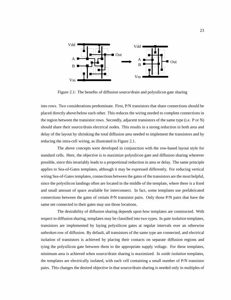
Figure 2.1: The benefits of diffusion source/drain and polysilicon gate sharing
into rows. Two considerations predominate. First, P/N transistors that share connections should be
placed directly above/below each other. This reduces the wiring needed to complete connections in
the region between the transistor rows. Secondly, adjacent transistors of the same type (i.e. P or N)
should share their source/drain electrical nodes. This results in a strong reduction in both area and
delay of the layout by shrinking the total diffusion area needed to implement the transistors and by
reducing the intra-cell wiring, as illustrated in Figure 2.1.
The above concepts were developed in conjunction with the row-based layout style for
standard cells. Here, the objective is to maximize polysilicon gate and diffusion sharing wherever
possible, since this invariably leads to a proportional reduction in area or delay. The same principle
applies to Sea-of-Gates templates, although it may be expressed differently. For reducing vertical
wiring Sea-of-Gates templates, connections between the gates of the transistors are the most helpful,
since the polysilicon landings often are located in the middle of the template, where there is a fixed
and small amount of space available for interconnect. In fact, some templates use prefabricated
connections between the gates of certain P/N transistor pairs. Only those P/N pairs that have the
same net connected to their gates may use those locations.
The desirability of diffusion sharing depends upon how templates are constructed. With
respect to diffusion sharing, templates may be classified into two types. In gate isolation templates,
transistors are implemented by laying polysilicon gates at regular intervals over an otherwise
unbroken row of diffusion. By default, all transistors of the same type are connected, and electrical
isolation of transistors is achieved by placing their contacts on separate diffusion regions and
tying the polysilicon gate between them to the appropriate supply voltage. For these templates,
minimum area is achieved when source/drain sharing is maximized. In oxide isolation templates,
the templates are electrically isolated, with each cell containing a small number of P/N transistor
pairs. This changes the desired objective in that source/drain sharing is needed only in multiples of
24
the template size.
2.1.2 Previous Cell Layout Systems
Despite the aforementioned differences, there remain enough similarities between the
Sea-of-Gates and standard cell layout styles to justify a review of the techniques developed for
automatic transistor level layout of such cells. The first such systems were designed to produce
layout of relatively small cells, typically 50 transistors or less. The seminal work in this field was
by Uehara and VanCleemput[47] who developed a technique for mapping logic functions expressed
as And-Or-Invert gates directly to pairs of CMOS transistors. They then presented a heuristic
algorithm for a linear ordering of the resulting transistors that maximizes diffusion abutments in the
resulting layout. Subsequently, exact algorithms for this transistor ordering were developed based
on finding and enumerating Euler paths[48].
Concurrently, systems were developed that would accept circuits not expressible as AOI
gates. The first such system was Sc2[49], which used heuristic algorithms similar to those used in
block placement systems. Later, Pinter et. al.[50] developed an exact algorithm for enumerating the
linear ordering of transistors and efficiently computing the layout cost of the orderings. All these
algorithms build up linear chains of transistors, and can use secondary criteria (wiring length and
density), to decide among chains of similar size. Furthermore, it is possible to compute the wiring
density and length of a chain accurately.
However, multiple row layouts become more desirable as cell sizes go beyond around 25
to 30 P/N pairs. The wiring of single row layouts become increasing inefficient relative to multiple
row ones as the number of transistor pairs increases. This is because average wiring length is
proportional to the length of a cell’s perimeter (bounding box). The perimeter is proportional to the
number of transistors for a single row layout but only proportional to the square root of the number
of transistors if the latter’s aspect ratio is allowed to remain near one. Even for cells that are small
enough for these algorithms, there may be the need to place the cells into multiple rows to satisfy
externally imposed aspect ratio constraints.
These limitations spurred the development of systems that could handle medium or large
numbers of transistors and place them into multiple rows[18][51]. These systems divide the problem
into a phase in which transistors are partitioned into groups and the groups placed followed by a
separate phase in which the transistors in a group are ordered. The partitioning phase relies on a
mincut algorithm to group transistors to minimize inter-group density and places them to minimize

25
net-length. Then the transistors are placed in a separate linear ordering step that maximizes diffusion
abutments.
While this approach has the advantage of being able to utilize the existing good algorithms
for two-dimensional block placement and linear transistor ordering, it creates problems as well.
First, using separate objective functions in the phases makes it difficult to make tradeoffs among the
different layout objectives. For instance, in Sea-of-Gates it is sometimes worthwhile to rank density
minimization higher than diffusion abutment maximization, since the height of a row is fixed.
Furthermore, with respect to wiring minimization, the problems of group and transistor
placement are interdependent. Calculations of wiring length in the group placement phase are
inaccurate when all wires are assumed to originate from the centers of the transistor clusters.
Hence, we must know the layouts of the clusters when we do cluster placement. However, the
wiring cost of a transistor placement may be strongly dependent on the cost of the wires that
must connect transistor groups. This in turn depends on the locations of the groups. Thus, while
each objective may be optimized for separately, trying to achieve both objectives by applying the
optimizations for each individual objective in sequence can produce a sub-optimal result.
2.2 SoGOLaR
SoGOLaR (Sea-of-Gates Optimized Layout and Routing) is a program that generates
functional cells in the Sea-of-Gates layout style. The input circuit may be specified as either a
schematic net-list or a list of boolean expressions where each expression specifies a multi-level AOI
tree. The desired size of the cell and desired pin positions may also be specified at the input. Cell
size may be constrained in one of two dimensions, while pins may be fixed either at exact track
locations or on a particular side of the cell boundary.
SoGOLaR will map the transistors given at the input to the grid produced by the Sea-
of-Gates templates in the manner that maximizes transistor site utilization (diffusion sharing) and
minimizes wiring length. Our overall strategy is to form a net-list of P/N transistor pairs and then to
place and route these pairs on a symbolic grid. By performing placement directly on P/N pairs, we
overcome the problem of hierarchical interaction. The objectives of maximizing diffusion sharing
and minimizing wiring length are handled by a single algorithm. Besides making tradeoffs between
these objectives easier, our method has the advantage that it also applies to cells that are laid out in
multiple rows. Also, this approach facilitates modeling different templates in the placement routine.
Here, the objective is to model as accurately as possible the characteristics of different Sea-of-Gates
26
templates. These considerations and our strategies for accommodating them are described in more
detail in the sections below.
2.2.1 P/N Transistor Pairing
The Sea-of-Gates layout style is designed to be used with a circuit design style that uses
fully restoring logic and memory circuits. In this design style, logic circuits are implemented by
separate networks of transistors for the “0” and “1” state of the output, these are called pull-down
and pull-up networks respectively. Memory circuits in this style use explicit pull-up transistors to
maintain the stored state. These are called static memory cells, partly for this reason the design
style itself is also called static CMOS. Usually, the pull-down and pull-up networks of static CMOS
circuits have the same number of transistors in them. Thus, most Sea-of-Gates templates use roughly
the same number of P and N type transistors.
We have chosen to pair P and N transistors in a separate step from transistor placement
because we can use specialized knowledge about the structure of static CMOS circuits to find
suitable pairs efficiently. This in turn increases the efficiency of the overall placement task by
reducing the number of objects handled by the next placement step. Our pairing algorithm takes
into account two objectives. First, we minimize the amount of routing that must cross the middle of
the cell by pairing those transistors that share a net. In Sea-of-Gates we are particularly interested
in sharing gate nets, in fact some templates require that certain transistor sites share the gate net.
Secondly, we must avoid overconstraining the ability of the next step to find chains of transistors
that share diffusion nets. Thus, whenever possible we must ensure that when pairing a P and an N
transistor, the transistors that share a diffusion connection with them are paired as well.
The first step of transistor pairing is to identify the common nodes in a circuit, these being
the circuit nodes that connect the P and N diffusion layers. We then trace the pull-up and pull-down
networks that begin at these common nodes until we reach either the supply or ground nodes or
another common node. At this point, we select those pull-up and pull-down networks that share
both their common nodes and try to pair the transistors in them. We do this by decomposing each
network into a hierarchy of series and parallel circuit paths. Each hierarchy is then rearranged
to match similar components using a technique similar to that found in Uehara[47]. In this step,
paths are considered similar if they have the same number and complexity of children. Now, the
transistors in matching paths are paired, with pairings graded according to the number of nets shared
by the paired transistors. A higher grade is given to shared gate nets relative to shared diffusion

27
nets. If more than one combination of P and N networks share both common nodes, we perform
this step on all combinations of networks and choose the best result.
If the pull-up and pull-down networks exhibit series/parallel duality, this technique will
always pair all of the transistors very quickly, and each pair will share a gate net. In networks
without this property, not all of the transistors may be paired at the end of this first step. Among
the remaining transistors, we give first priority to pairing transistors within matched networks (i.e.
networks that share both beginning and end nodes) and which have unique gate nets (i.e. only those
two transistors share that gate net). When two possible pairings of transistors have equal value (e.g.
two P and two N transistors share the same gate net), we search the transistors that connect to the
source and drain of each potential pair. We choose to pair those transistors whose source/drain of
each transistor are connected to an already formed pair. Those transistors left over from this step
are paired with transistors from outside the matched networks using similar heuristics.
We have found that these heuristics are sufficient to pair all of the circuits encountered
with good results. While not all static CMOS circuits have pull-up and pull-down networks that
are series/parallel dual, every circuit encountered has been at least partially decomposable in this
fashion. Starting from these pairings, our algorithm was always able to derive good pairings for
transistors in non-series/parallel sections of the network. The complexity of the most productive step
(series/parallel decomposition and matching) is linear in the number of transistors. Subsequently
steps requireO(N 2) or higher complexity, yet the overall algorithm remains highly efficient because
the more expensive steps are used on relatively few transistors.
2.2.2 Transistor Pair Placement
Given the net-list of paired transistors, we are now ready to find a placement for them.
We start by defining an abstract rectangular array of P/N pair placement sites, called slots, with one
slot corresponding to one Sea-of-Gates template. We model the placement step as an assignment of
transistor pairs to these slots. We use this abstraction because it allows us to model the particulars of
a Sea-of-Gates template easily by annotating the slot array. For example, templates that use oxide
separation are modeled by marking particular slots with the template boundaries. Slots may also be
labeled to reflect a pre-fabricated gate connection, only P/N pairs with matching P/N gate nets will
be assigned to those slots. The details of exactly how slots are annotated and how the placement
algorithm uses the annotation are given in the section on template comparison.
After placement, the transistor pairs are mapped to the Sea-of-Gates templates according
28
to their slot assignment. Because the slot assignment already models the properties of the particular
template, the final mapping uses a a straightforward assignment of each row of P/N pairs from left
to right.
The number of rectangular slots and the dimensions of the slot array are determined
prior to placement and remain static throughout the placement procedure. Since the creation of
unused sites is taken into account in the placement cost function, we allocate only enough slots
to accommodate all the P/N pairs. The allocated number of slots is then split evenly into rows
according to the desired dimensions for the cell. If unconstrained, the number of rows is chosen to
produce a cell that is square or with slightly more width than height. Constraints on cell height are
accommodated by simply choosing the greatest number of rows that does not exceed that constraint.
When a constraint on module width is specified, the selection of rows is complicated by the fact
that we do not know the final module width until after placement because some template sites will
remain unused. If a module width constraint is specified, we reduce the number of slots assigned
to each row by an amount equal to the estimated fraction of unused sites per row. This value is
computed separately for each template style, and is derived by averaging the results from previously
run modules with that template style. Finally, the number of slots is always “rounded up” to ensure
that each row contains the same number of slots.
To perform the assignment of transistor pairs to slots, we have chosen the optimization
method of simulated annealing. Simulated annealing is a general technique for solving combinato-
rial optimization problems[52] that was derived from principles discovered in the study of statistical
mechanics and thermodynamics[53]. The algorithm may be viewed as simulating the process of
annealing, whereby a material is melted and then cooled slowly to achieve a well ordered (e.g.
crystalline) state.
In its general form, the inputs to the simulated annealing algorithm consist of a set of
states S, a cost function C(s) defined on all states s 2 S, and a move function M(s) that provides
a one to many mapping of the set of states onto itself. Given these inputs, the algorithm begins by
randomly selecting an initial state s0 and generating a new state s1 by applying the move function.
This move is accepted (i.e. s1 becomes the current state) with probability
p(∆C) =
8<:
1 if ∆C <= 0
exp(∆C=T ) if ∆C > 0
where ∆C = C(s1)� C(s0).
The parameter T , which governs the probability of accepting a cost increasing move, is
29
referred to as the annealing temperature. This parameter is set sufficiently high at the start to allow
almost all cost increasing moves and lowered by a monotonic cooling schedule until a “freezing”
temperature is reached at which almost no cost increasing moves are accepted. At each temperature,
a sufficient number of moves must be performed to allow the optimization to reach equilibrium.
Reaching equilibrium at the “freezing” temperature implies that the resulting state is (with high
probability) a minima, i.e. no move from that state decreases the cost function. At this point, the
algorithm ends and the current state is returned as the final output.
The general description purposely leaves out the details of choosing the initial temperature,
cooling schedule, equilibrium condition and final temperature. This is because these parameters
must be determined experimentally for the particular optimization problem to be solved. Although
asymptotic convergence properties have been derived for the general algorithm[54], there is no
guarantee (not even a probabilistic one) of finding the absolute (global) minimum of the cost
function C within a finite number of moves.
Despite the lack of convergence guarantees for a practical cooling schedule, simulated
annealing was successfully applied to the problem of placing blocks in a standard cell layout
system[55]. Here the set of states is the set of all possible block placements, and a move consists of
either interchanging two blocks or displacing a single block to a new location. Although no guar-
antees can be made regarding finding the global minimum, these initial experiments demonstrated
that simulated annealing has a higher probability of escaping high cost local minima compared
to “force-directed” or “greedy” algorithms that never accept cost increasing moves. These initial
results favorable provided the motivation to apply the simulated annealing algorithm to problems
such as macro-block placement[56], the two-dimensional compaction of array logic structures[57],
and single row transistor placement[58].
Concurrently, further experiments were performed with the objective of optimizing the
many control parameters in the simulated annealing cooling schedule. Our own experiments
indicate that our results are relatively insensitive to changes in these parameters; thus we do not
give a comprehensive detailed discussion of these experiments here. Instead, the paragraph below
gives these parameters as they are used in SoGOLaR; interested readers will find the derivations in
the references cited.
The initial temperature T0 must be set to a value large enough for almost all moves to be
accepted regardless of the difference in cost. We find this temperature by taking a sample of 100
30
moves to find the standard deviation of the cost function with respect to the initial state S01 and
setting T0 to a value that is fifteen (15) times this standard deviation[59]. At each temperature, the
algorithm is run until thirty 30 moves are accepted; this constitutes our “equilibrium” condition.
The temperature is then lowered according to the formula:
Tnew = � � Told
We have gotten good results with � set to 0:9[60].
We terminate the algorithm if the temperature has been decreased and equilibrium re-
established three consecutive times and the cost function has not decreased. Note that this stopping
criterion does not guarantee that the final placement is at a minima or is even the lowest cost
placement seen. To recover the lowest cost placement after some cost increasing moves, we
record the entire placement at each temperature change along with each accepted move at a given
temperature and the index of the last move whose resulting placement had the lowest cost. This
latter bit of information ensures that if we will “undo” the moves at a given temperature to find the
lowest cost placement but not undo moves prior to that if they did not increase or decrease the cost.
This placement is then sent to a greedy post-processing step that looks at every move possible but
only accepts cost decreasing ones. We iterate until a placement is found for which no possible move
decreases the cost; this placement is, by definition, at a minimum and is returned as the final result.
Because our result are relatively insensitive to cooling schedule details, we have been
able to focus our effort on those elements of the algorithm where specific knowledge of transistor
placement must be included in order to simultaneously reduce both net-length and diffusion breaks.
In SoGOLaR, these elements are the method used to generate a new placement (move generation),
the method used to evaluate the cost of a placement and the methods used to balance the disparate
terms of said cost function. We outline our approach to each of these elements below, leaving those
details that are applicable to only one Sea-of-Gates template style to the comparative discussion of
template styles in the next section.
In SoGOLaR, moves are generated by interchanging the contents of randomly selected
locations in the slot array. Most of the generated moves are interchanges of transistor pairs; one
of the slots chosen may be empty since there may be more slots than transistor pairs. The basic
interchange step is augmented by a search of adjacent transistor pairs whose objective is to find
locally optimal transistor configurations. These adjustments substantially reduce the number of
“bad” moves generated without affecting the final result. Because the method of search is governed
1The initial state is never altered in this step (i.e. no moves are accepted)
31
by SoGOLaR’s model of different template styles, the details of move generation are described with
that model in the template comparison section.
The choice of objectives to evaluate a new placement is driven by the geometry of Sea-
of-Gates layout. In Sea-of-Gates the height is determined by the number of rows in the layout, for
small cells one cannot change the number of rows without substantially altering the geometry of the
layout. For this reason, the placement objective becomes width minimization, i.e. to pack as many
transistor pairs as possible into the chosen number of rows.
For the layout to be realized, the transistor pairs must also be routable in the chosen
packing. Wire-ability is a function of both the length of the wires to be connected and the maximum
density, defined as the number of wires crossing a given cut line. For small cells, we are most
concerned with the density of the wiring that runs within the transistor rows. That is because there
are more wires in that direction, less space, and it is not possible to add extra space in that direction
for overflow wires.
In order for the placement process to be efficient, we must convert these objectives into a
readily computable cost function. SoGOLaR uses the following cost function:
CF = NL+ �1W + �2∆W
whereNL is the overall wiring length of the layout,W is the overall width of all rows in the layout,
and ∆W is the difference in width between the widest and narrowest row. The quantity NL is the
sum of the half-perimeter wiring length of all nets in the layout. We chose wiring length as our
measure of wire-ability because compared to density the wiring length function is easier to compute
and more discriminating of differences among layouts. The components of this cost function are
illustrated for a sample slot array in Figure 2.2.
To get good results, we must ensure that the scaling coefficients �1 and �2 are set such
that the effects of one component of the cost function do not dominate the other components. Since
the probability of move acceptance is proportional to the change in cost function ∆C caused by
the move, we adjust �1 and �2 according to the contribution of each component to ∆C. To do
this, we sum the contributions to ∆C from the components NL and W + ∆W for all accepted
moves. We adjust the scaling coefficients for a given temperature based on the data collected at the
previous temperature. We also adjust the relative amount of contributions from the two components
as annealing progresses. For best results, we start with a nominal contribution from the W + ∆W
component, increasing it gradually until the contributions are roughly equal during the critical
stages of annealing (i.e. the temperatures where the cost function decreases the most). The width
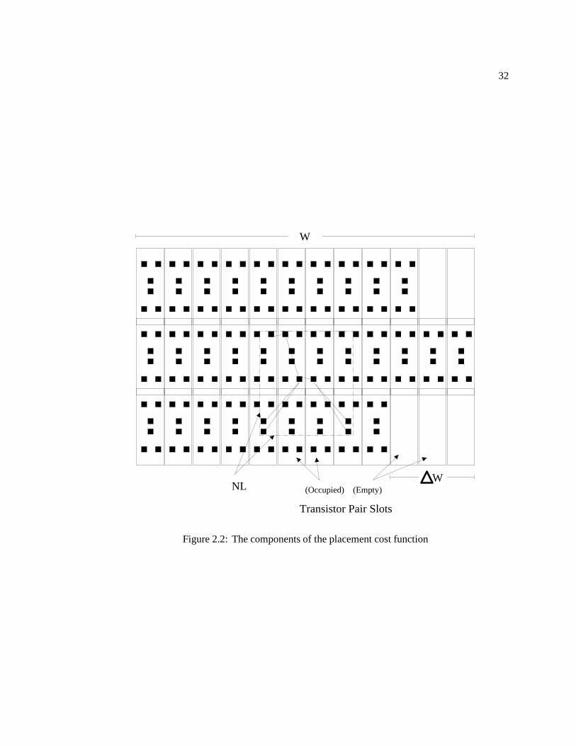
32
W
WNL
Transistor Pair Slots
(Occupied) (Empty)
Figure 2.2: The components of the placement cost function
33
contribution is then increased a little more during the final annealing stages to ensure good packing
in the final placement.
When the placement of pairs into slots is complete, we finish the placement step by
converting the abstract slot array into an array of templates of the given type. Since the properties
of the given template are incorporated into the placement cost function and move selection, this
step involves a simple left to right mapping of each row of transistor pairs. The resulting array of
templates is augmented with empty templates if needed to equalize the width of each row. This
array is the final output of the placement stage.
2.2.3 Module Wiring
The wiring of the modules produced by the placement stage is complicated by the dif-
ferences among Sea-of-Gates template styles. Each template style has its own set of locations
for source/drain contacts and its own wiring pitch. A given template style may contain obstacles
that prohibit wires or vias. Prefabricated connections may also exist, particularly between two
polysilicon gate landings. Both the flexibilities and the constraints must be modeled accurately in
order to obtain good routing results.
In many cell generation systems, such as GENAC[61], routing is accomplished using
a model that partitions the row of transistors into several channels. This approach has proven
suitable for row based layout where transistor sites are not fixed. However, the use of multiple fixed
polysilicon landings and via obstacles in Sea-of-Gates presents severe difficulties for any approach
that relies purely on channel routing.
In SoGOLaR, module wiring is performed by a general area router augmented by a pre-
processing stage. The pre-processing stage first wires those nets whose pins lie entirely on one
diffusion row in first layer metal. We use a greedy left edge algorithm that assigns tracks in order
from the outermost track (i.e. the ones closes to the power rails) toward the polysilicon landings of
each cell. After whole nets are routed, we next wire segments of nets where at least two pins are on
the same diffusion row. Such a segment is routed if and only if it does not increase the number of
tracks already occupied by wires.
Since the pre-processed segments are selected and routed in time proportional to the
number of pins, these steps are less complex compared to using the general area router. While the
area router has the ability to move or even rip up the results of this stage, this occurs very rarely in
practice. Thus, the pre-processor reduces the overall complexity of the wiring step.
34
SoGOLaR then invokes the CODAR[37] general area router to complete the partially
wired module. CODAR employs a global routing algorithm that uses an estimate of congestion in
various areas of the cell, based on the combined effect of the fixed devices, previously placed nets,
and other types of obstacles. A first constructive routing phase results in a rough placement of all
the nets in the cell in promising but not necessarily conflict-free locations. Insulated wire segments
are used to cross obstacles or other wires on the same routing layer.
In the subsequent refinement phase, a detailed routing algorithm tries to rearrange the
wiring so that it can be implemented without any conflicts. It relies on a shallow recursive search
using local modification moves to relocate pieces of nets that contain insulated wire segments. If
not all insulated wires can be eliminated by local modification moves, the program may rip-up an
entire net and call again on the global routing algorithm to find a less congested course from which
the search through local modification moves is restarted.
The two algorithms, global and detailed routing, are tightly integrated and work on the
same data structure representing the virtual grid of tracks. This integration has resulted in a router
that can solve difficult problems not solvable by other programs while exhibiting run-times that
grow only moderately with the size of the routing problem.
2.3 A Comparative Study of Sea-of-Gates Template Styles
Since the use of a pre-fabricated transistor array is the primary distinguishing factor in
the Sea-of-Gates layout style, the success of this style is critically dependent on the design of the
transistor geometry. Since the amount of functionality that can be put into one Sea-of-Gates chip
is proportional to the number of transistors on that chip, nearly all transistor array geometries are
designed to pack as many transistors as closely as possible onto the chip.
This objective is balanced by the need to choose a single (or at most, two) transistor size(s)
for the pre-fabricated array. Uniformly increasing the size of all transistors has (to a first order) a
very small effect on delay, because the increase in drive capability is offset by the increase in internal
circuit capacitances. By this analysis, the ideal transistor size is the minimum size sufficient to
drive a medium amount of inter-cell wiring capacitance without long delays or the need for special
booster cells. This minimum threshold has been shown to be quite small, usually on the order of
four to six times the minimum possible transistor size[62].
Despite what appears to be a relatively simple and uniform objective, a wide variety of
base cell templates have been developed for Sea-of-Gates arrays. A few of the variations reflect
35
a desire to accommodate secondary objectives, such as including analog circuits[63], or dynamic
CMOS circuits[64] in the array. Even among arrays intended for our chosen class of circuits, namely
digital static CMOS circuits whose wiring is implemented with two layers of metallization, base
cell templates differ in several ways, including:
� The method used to electrically isolate adjacent transistors on a row when said transistors
belong to different circuits.
� Whether or not the gates of adjacent P- and N- transistor pairs are connected with polysilicon.
� The targeted location for power and ground wiring.
� The organization of transistor rows (i.e. NPNP versus NPPN arrangement).
At least some of this variance is explained by the difficulties of determining the influence
of template design on the quality of circuit layout. Template designers studying this interaction have
been limited by the amount of time required to implement a large number of circuits in a particular
template style. This is reflected in the fact that several templates have been designed to implement
a particular kind of circuit[65][66] or a small customized library of cells[67] well.
The objective of this study is to overcome this difficulty by using SoGOLaR to implement
a variety of circuits on several Sea-of-Gates template styles. We begin by looking at the details of
various template styles and choosing a representative set of templates whose characteristics are most
suited for for automatic, on-demand cell generation. We then illustrate how SoGOLaR captures the
differences among template styles with a parameterized model. The use of a parameterized model
in SoGOLaR is crucial because it allows new template styles to be incorporated without modifying
the structure of the program.
Lastly, we present the results of using SoGOLaR to implement a set of small to medium
sized combinational logic circuits in our chosen template styles. In presenting our results, we
attempt to answer two questions, namely:
� How do differences in template connectivity characteristics (i.e. isolation technique and
presence of pre-connected gates) affect the results of automatic cell synthesis?
� What dimensions (i.e. width and height) should a template in each style have in order for all
internal circuit wiring to be completed without adding extra unused rows and/or columns?
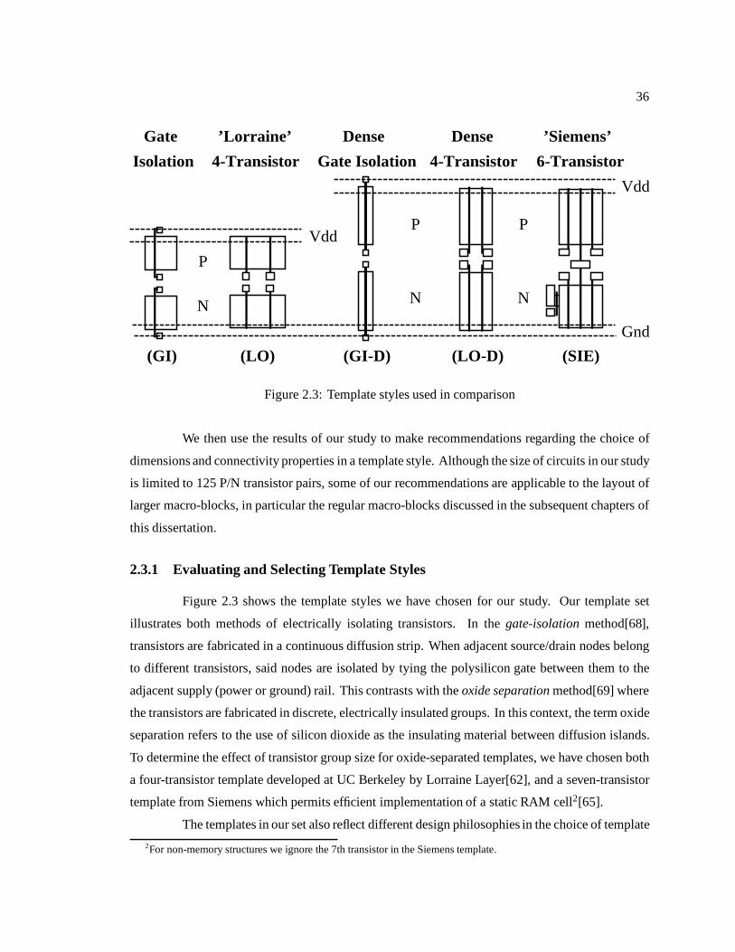
36
4-Transistor 6-Transistor
’Lorraine’ ’Siemens’
(LO) (SIE)(GI) (GI-D)
Gate
Isolation 4-TransistorGate Isolation
Dense
(LO-D)
Dense
Gnd
Vdd
Vdd
P
N N
P P
N
Figure 2.3: Template styles used in comparison
We then use the results of our study to make recommendations regarding the choice of
dimensions and connectivity properties in a template style. Although the size of circuits in our study
is limited to 125 P/N transistor pairs, some of our recommendations are applicable to the layout of
larger macro-blocks, in particular the regular macro-blocks discussed in the subsequent chapters of
this dissertation.
2.3.1 Evaluating and Selecting Template Styles
Figure 2.3 shows the template styles we have chosen for our study. Our template set
illustrates both methods of electrically isolating transistors. In the gate-isolation method[68],
transistors are fabricated in a continuous diffusion strip. When adjacent source/drain nodes belong
to different transistors, said nodes are isolated by tying the polysilicon gate between them to the
adjacent supply (power or ground) rail. This contrasts with the oxide separation method[69] where
the transistors are fabricated in discrete, electrically insulated groups. In this context, the term oxide
separation refers to the use of silicon dioxide as the insulating material between diffusion islands.
To determine the effect of transistor group size for oxide-separated templates, we have chosen both
a four-transistor template developed at UC Berkeley by Lorraine Layer[62], and a seven-transistor
template from Siemens which permits efficient implementation of a static RAM cell2[65].
The templates in our set also reflect different design philosophies in the choice of template
2For non-memory structures we ignore the 7th transistor in the Siemens template.
37
height. For instance, the original form of the Siemens template provides nine unblocked first layer
metal tracks running across the P/N transistor pairs, while the original “Lorraine” template has only
four such tracks. The Siemens template is designed to be large enough to accommodate all the
wiring needed for circuits of small or medium size. In contrast, the original “Lorraine” template
was designed to be the minimum size needed to implement a library of small (< 15 P/N pairs) cells
with transistors just large enough to drive a medium sized wiring capacitance. This minimum height
is, however, readily adjustable through the “Mariner”[25] template generator program.
The chosen templates differ greatly in their horizontal dimensions as well. The three
transistor pairs in the Siemens cell are at the same spatial pitch as the overlying second layer metal
tracks. The basic ‘Lorraine’ cell spaces the two transistor pairs by an additional track in second
layer metal. To separate the influence of the various template parameters, we added to our study
versions of the four-transistor and gate-isolation template styles that use only one vertical track per
transistor pair.
Our choice of templates reflects a conscious decision to adopt certain template de-
sign conventions. All of the template styles mirror alternating rows of templates to produce a
NPPNNPPN: : : row pattern. This allows a wide power supply bus to serve two adjacent rows of
transistors at a time, rather than running a smaller bus down every diffusion row as would be nec-
essary with a NPNPNPNP: : : pattern. Although at least two template style[68][69] use the NPNP
arrangement, neither appears to be more area efficient than the templates we have chosen.
Lastly, we have avoided templates that pre-connect the gates of a large block of P/N
transistor pairs. At least two template styles[66][67] use oxide-separated templates containing three
P/N pairs where the gates of each pair are pre-connected. These pre-connected gates cannot be
used whenever the inputs to the P- and N- sides of the pair must differ, such as the inputs to a
static CMOS transmission gate. Thus, at least some P/N pairs must have independent inputs. The
Hitachi template[66] intersperses separate rows of small transistors above and below the main (pre-
connected) rows to form a pPNn arrangement. The Motorola template[67] uses eight transistors
(four P/N pairs) where three of the pairs are pre-connected.
Because transmission gates make up only a tiny fraction of the transistors in static CMOS
net-lists, the Hitachi template is area inefficient in that the small transistors are difficult to use in any
other type of circuit because of their placement. The Motorola template doesn’t have this problem,
but mixing independent and pre-connected pairs on the same template means that the area needed
for polysilicon landings between P- and N- transistors is only slightly less than would be needed if
all pairs were independent.
38
Pre-connected transistors also make it impossible to electrically isolate one pair of transis-
tors from another pair on the same template. In oxide-separated templates, this occurs whenever the
number of transistors that may be placed on a continuous strip of diffusion is not an exact multiple
of the template size. By carefully choosing the circuits to be implemented, it can be guaranteed that
these odd-sized strips always have either an output or a supply node at one end. Unused source/drain
nodes may simply be connected in parallel with the supply node in the circuit, while a transistor
connected to the output may be connected in parallel with unused ones to increase the output drive
capability. This means that although these templates can be used with customized cell libraries, they
are incompatible with our objective of supporting on-demand cell generation of any static CMOS
circuit. Lastly, note that unused transistors in the Siemens cell may always be isolated, despite the
existence of a single pair of pre-connected gates, by tying the independent gates at either end to
their respective supply rails.
2.3.2 Modeling Template Styles in SoGOLaR
In this section, we discuss how SoGOLaR handles different template styles. In our
approach, we avoid customizing the cost function evaluation and move generation for each template
style. Instead, we use fixed placement routines that use the relevant properties of each template style
as input. This allows a user to add a new template style without modifying SoGOLaR’s code and
without having to consider the details of our optimization algorithm. Existing placement algorithms
already use this approach with respect to the geometric properties of blocks, such as block size and
pin positions. SoGOLaR extends this concept by explicitly representing the connectivity properties
of a template (i.e. the pre-fabricated connections among transistor terminals) as constraints that are
used by the move generation and cost evaluation routines to guide the packing of transistor pairs
into a minimal number of templates.
In SoGOLaR, template connectivity is evaluated by superimposing on the slot array a
grouping that represents instances of the target template style. This grouping structure allows us
to quickly determine whether a new template must be created (or destroyed) whenever a transistor
pair is moved to a new location in the slot array. Each newly created group adds to the length of the
row where it is located and is thus reflected in the placement cost function. No attempt is made to
model the increase in net-length caused by adding a template. Although row length and net length
are strongly correlated, measuring row length only means that adding a template incurs the same
penalty no matter where that template is located. If net length was also measured, templates nearer
39
the center of the module would cost more since more nets would be lengthened. We experimented
with and rejected the idea of increasing the template creation penalty in areas near the center of the
module. We found that a fixed template creation penalty was sufficient to ensure that no empty slots
appeared near the center of any SoGOLaR produced module.
To minimize the number of new templates created by moves, the move generation routines
try to merge the newly placed transistor pairs with the transistor groups immediately adjacent on
either side. The procedure used for this search depends on the type of template targeted. For oxide
separation templates, all possible arrangements of transistor pairs in the group are attempted and
the minimum cost arrangement chosen. For gate isolation templates, merging is only attempted at
the ends of existing transistor pair groups, except when a pair can be attached to an existing group
through the power supply nets. If the cost of the resultant grouping is still too high, the search is
expanded to include one more set of adjacent groups.
At each step, the decision to create or destroy a group of transistor pairs is made by
a predicate function that takes a list of pairs and their prospective template positions. It is this
predicate that uses the connectivity constraint expressions to make its decision. In this way, the
search procedure remains fixed for all template styles, yet new template styles can be added easily.
2.3.3 Using SoGOLaR to Evaluate Template Styles
Although reasoning about the details of template styles can eliminate some candidate
styles as obviously unsuitable for on-demand cell generation, several stylistic differences remain
whose effects on cell generation are difficult to predict. To illustrate and evaluate these effects, we
have used SoGOLaR to implement a select spectrum of cells on our chosen templates. These cells
range from small examples with only 20 P/N pairs to medium sized ones with over 100 pairs.
In developing the method for our study, we have taken several steps to simplify our
evaluation task and to avoid introducing a bias in favor of a particular template style. First, we
restrict our cell set to combinational logic, implemented as static CMOS circuits with dual networks
for pull-up and pull-down. These examples were processed by the MIS logic synthesizer[70] and
mapped to a representation consisting of small to medium sized AOI gates. To avoid long diffusion
strips which would favor gate isolation templates, we limit the maximum size AOI gate to three
levels of logic with three inputs per level. In placing the resulting transistor pairs, we use as tight a
packing as possible in order to evaluate the effects of each template style on routing congestion. In
routing the cells, we use a wiring grid with uniform pitch and permit the use of both metal layers in
40
either direction, but rely on a routing cost function that strongly discourages the use of second level
metal in the horizontal direction.
Site Utilization and Horizontal Density
We begin our study by attempting to capture the effects of template connectivity inde-
pendent of the dimensions of a template. To this end, we first measure site utilization, namely the
fraction of P/N transistor slots used for implementing the net-list, out of all the slots available in the
templates that are fully or partially used. For gate-isolation templates site utilization is given by:
SU =NLP
NLP + I
where NLP is the number of transistor pairs in the net-list and I is the number of isolation gates
needed. For oxide-isolated templates, the formula is
SU =NLP
n � T
where T is the number of template sites with at least one transistor pair used, and n is the number
of transistor pairs in one site. This measure does not include leftover space due to unevenness of
the length of the occupied parts of individual template rows.
In Table 2.1 we present site utilizations for the three different template connectivity types
studied. The four-transistor template has the best utilization; the placements in this template style
leave at most one template partially filled. This template style benefits from the fact that we need
only find groups of two transistor pairs to completely utilize a template. The gate isolation and
six-transistor template styles both use approximately 70% of the available sites for transistor pairs.
The figures shown for the gate isolation and six-transistor template styles do not represent
the absolute maximum site utilization possible. A balance must be found between maximizing
source/drain sharing and minimizing net length, and some potential abutments are ignored because
they result in a placement with too high a net length. This effect is most pronounced in the
six-transistor template style.
To quantify the effect of site utilization on area efficiency, we must look at transistor
density or the number of transistor sites per unit area. Since the height of a template can be readily
varied by adding more tracks in first level metal, we are concerned most about horizontal density.
Here we group the templates into two classes. One class of templates uses two vertical tracks per P/N
pair, as exemplified by the Lorraine template and by the (loose) gate-isolation template. In the other
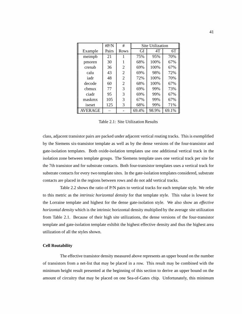
41
#P/N # Site UtilizationExample Pairs Rows GI 4T 6Tmeimpb 21 1 75% 95% 70%pmoren 30 1 68% 100% 67%crenab 36 2 69% 100% 67%
calu 43 2 69% 98% 72%iadr 48 2 72% 100% 70%
decode 60 2 68% 100% 67%cbmux 77 3 69% 99% 73%ciadr 95 3 69% 99% 67%
maskmx 105 3 67% 99% 67%iseset 125 3 68% 99% 71%
AVERAGE – - 69.4% 98.9% 69.1%
Table 2.1: Site Utilization Results
class, adjacent transistor pairs are packed under adjacent vertical routing tracks. This is exemplified
by the Siemens six-transistor template as well as by the dense versions of the four-transistor and
gate-isolation templates. Both oxide-isolation templates use one additional vertical track in the
isolation zone between template groups. The Siemens template uses one vertical track per site for
the 7th transistor and for substrate contacts. Both four-transistor templates uses a vertical track for
substrate contacts for every two template sites. In the gate-isolation templates considered, substrate
contacts are placed in the regions between rows and do not add vertical tracks.
Table 2.2 shows the ratio of P/N pairs to vertical tracks for each template style. We refer
to this metric as the intrinsic horizontal density for that template style. This value is lowest for
the Lorraine template and highest for the dense gate-isolation style. We also show an effective
horizontal density which is the intrinsic horizontal density multiplied by the average site utilization
from Table 2.1. Because of their high site utilizations, the dense versions of the four-transistor
template and gate-isolation template exhibit the highest effective density and thus the highest area
utilization of all the styles shown.
Cell Routability
The effective transistor density measured above represents an upper bound on the number
of transistors from a net-list that may be placed in a row. This result may be combined with the
minimum height result presented at the beginning of this section to derive an upper bound on the
amount of circuitry that may be placed on one Sea-of-Gates chip. Unfortunately, this minimum
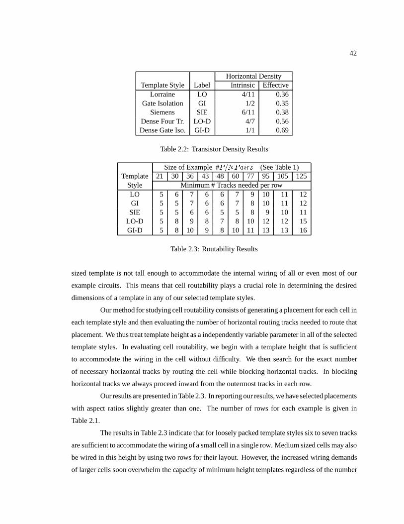
42
Horizontal DensityTemplate Style Label Intrinsic Effective
Lorraine LO 4/11 0.36Gate Isolation GI 1/2 0.35
Siemens SIE 6/11 0.38Dense Four Tr. LO-D 4/7 0.56Dense Gate Iso. GI-D 1/1 0.69
Table 2.2: Transistor Density Results
Size of Example #P=NPairs (See Table 1)Template 21 30 36 43 48 60 77 95 105 125
Style Minimum # Tracks needed per rowLO 5 6 7 6 6 7 9 10 11 12GI 5 5 7 6 6 7 8 10 11 12SIE 5 5 6 6 5 5 8 9 10 11
LO-D 5 8 9 8 7 8 10 12 12 15GI-D 5 8 10 9 8 10 11 13 13 16
Table 2.3: Routability Results
sized template is not tall enough to accommodate the internal wiring of all or even most of our
example circuits. This means that cell routability plays a crucial role in determining the desired
dimensions of a template in any of our selected template styles.
Our method for studying cell routability consists of generating a placement for each cell in
each template style and then evaluating the number of horizontal routing tracks needed to route that
placement. We thus treat template height as a independently variable parameter in all of the selected
template styles. In evaluating cell routability, we begin with a template height that is sufficient
to accommodate the wiring in the cell without difficulty. We then search for the exact number
of necessary horizontal tracks by routing the cell while blocking horizontal tracks. In blocking
horizontal tracks we always proceed inward from the outermost tracks in each row.
Our results are presented in Table 2.3. In reporting our results, we have selected placements
with aspect ratios slightly greater than one. The number of rows for each example is given in
Table 2.1.
The results in Table 2.3 indicate that for loosely packed template styles six to seven tracks
are sufficient to accommodate the wiring of a small cell in a single row. Medium sized cells may also
be wired in this height by using two rows for their layout. However, the increased wiring demands
of larger cells soon overwhelm the capacity of minimum height templates regardless of the number

43
of rows used in placement. While increasing template height provides greater routing capacity, the
added height does not significantly increase the complexity of examples that could be routed. This
occurs because the density of routing in the center of the cell increases much more quickly than
at the edges, thus much of the extra space added by increasing template height cannot be used for
internal wiring. This congestion affects the loosely packed and the densely packed template styles
equally.
Table 2.3 also shows that the routability of a cell is a function of the horizontal density for
a particular template style. In particular, the dense version of the four-transistor template (LO-D)
requires one to two more routing tracks to route an example than does the Lorraine cell (LO).
The dense gate isolation template (GI-D) requires three to four tracks more than its loosely packed
counterpart (GI). The dense cells suffer from a lack of space for vias and wiring turns. This space
is very important when routing output nets and making connections between the inputs of different
transistor pairs. In template styles with two vertical tracks per P/N pair, these turns and vias may be
placed to one side of the polysilicon landings. In template styles with high horizontal density, these
turns must be placed either above or below the landing, thus blocking horizontal routing tracks. A
simple example of this blockage is shown in Figure 2.4.
This effect is illustrated in Table 2.4,where we present the area of the maximally horizontal
cells listed in Table 2.3 with the entries in the table sorted by template area per transistor pair. The
data in this table represent routing area, this being the area of the cell using the minimum template
height needed to complete the routing of that cell. In computing area per transistor pair, we chose
a template height of eight free tracks for all styles.
From the table we see that while the dense gate-isolation pair has by far the lowest area
per transistor pair, its routing area is only slightly smaller than that of the dense four-transistor
cell. This occurs because the greater horizontal density of the gate isolation cell is offset by its
requirement for increased template height. The loosely packed template styles all have significantly
larger routing areas, indicating that these styles provide more vertical routing space than is needed
by our examples.
Lastly, in Figures 2.5 through 2.7 we present the layout of a cell with 36 P/N pairs for
each of the three template connectivity types used in our study. These figures are scaled to reflect
the actual relative sizes of the layouts.
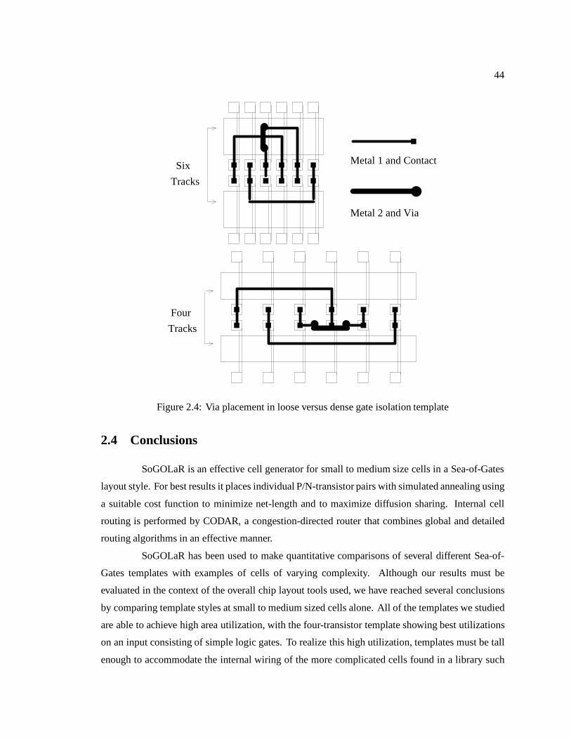
44
Metal 1 and Contact
Metal 2 and Via
Tracks
Tracks
Six
Four
Figure 2.4: Via placement in loose versus dense gate isolation template
2.4 Conclusions
SoGOLaR is an effective cell generator for small to medium size cells in a Sea-of-Gates
layout style. For best results it places individual P/N-transistor pairs with simulated annealing using
a suitable cost function to minimize net-length and to maximize diffusion sharing. Internal cell
routing is performed by CODAR, a congestion-directed router that combines global and detailed
routing algorithms in an effective manner.
SoGOLaR has been used to make quantitative comparisons of several different Sea-of-
Gates templates with examples of cells of varying complexity. Although our results must be
evaluated in the context of the overall chip layout tools used, we have reached several conclusions
by comparing template styles at small to medium sized cells alone. All of the templates we studied
are able to achieve high area utilization, with the four-transistor template showing best utilizations
on an input consisting of simple logic gates. To realize this high utilization, templates must be tall
enough to accommodate the internal wiring of the more complicated cells found in a library such
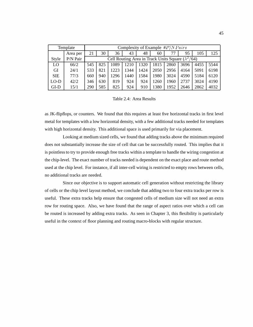
45
Template Complexity of Example #P=NPairsArea per 21 30 36 43 48 60 77 95 105 125
Style P/N Pair Cell Routing Area in Track Units Square (�2=64)LO 66/2 545 825 1089 1210 1320 1815 2860 3696 4455 5544GI 24/1 533 821 1223 1344 1424 2050 2956 4164 5091 6198SIE 77/3 660 940 1296 1440 1584 1980 3024 4590 5184 6120
LO-D 42/2 346 630 819 924 924 1260 1960 2737 3024 4190GI-D 15/1 290 585 825 924 910 1380 1952 2646 2862 4032
Table 2.4: Area Results
as JK-flipflops, or counters. We found that this requires at least five horizontal tracks in first level
metal for templates with a low horizontal density, with a few additional tracks needed for templates
with high horizontal density. This additional space is used primarily for via placement.
Looking at medium sized cells, we found that adding tracks above the minimum required
does not substantially increase the size of cell that can be successfully routed. This implies that it
is pointless to try to provide enough free tracks within a template to handle the wiring congestion at
the chip-level. The exact number of tracks needed is dependent on the exact place and route method
used at the chip level. For instance, if all inter-cell wiring is restricted to empty rows between cells,
no additional tracks are needed.
Since our objective is to support automatic cell generation without restricting the library
of cells or the chip level layout method, we conclude that adding two to four extra tracks per row is
useful. These extra tracks help ensure that congested cells of medium size will not need an extra
row for routing space. Also, we have found that the range of aspect ratios over which a cell can
be routed is increased by adding extra tracks. As seen in Chapter 3, this flexibility is particularly
useful in the context of floor planning and routing macro-blocks with regular structure.
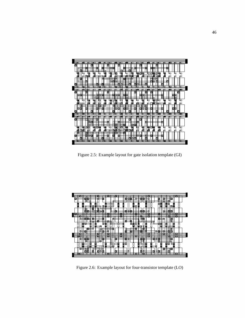
46
Figure 2.5: Example layout for gate isolation template (GI)
Figure 2.6: Example layout for four-transistor template (LO)
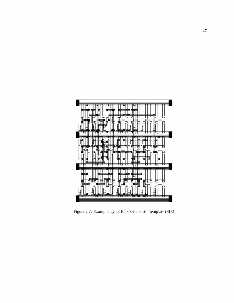
47
Figure 2.7: Example layout for six-transistor template (SIE)
48
Chapter 3
Efficient Layout of Regular
Macro-modules in Sea-of-Gates
Special purpose tools are used for the layout of regular macro-modules for the same reason
they are used in transistor-level layout, namely to take advantage of the particular structure present
in the input net-list. Whereas transistor-level layout techniques rely on the uniform shape and pin
configuration of transistors, techniques for the layout of regular macro-modules take advantage of
the organization of the macro-module into arrays of identical cells1.
This organization is best illustrated by considering the layout of a single array of identical
cells, such as a memory function block (i.e. RAM, ROM or register file) consisting of m words of
independently addressed memory with each word containing n bits. This block would be laid out
as a two dimensional array of cells, with columns corresponding to all of the bits in a given memory
word and rows corresponding to a specific bit in each memory word. Each memory cell instance
therefore has a data bit line connection running through it in one direction, say left to right, and a
word address line running in the orthogonal direction (top to bottom).
In laying out the memory cell, the bit and word lines are routed through the cell such
that the pins at the edge of the cell are placed at matching locations on opposite sides of the cell.
Thus, the layout of the base cell of an array contains not only its own wiring but also the external
wiring that must pass through it in order to wire the array. The entire array including the inter-cell
wiring is formed by replicating the base cell and abutting the resulting instances. This layout
technique, known as cell assembly[40], avoids using specially designated space for external wiring
1Throughout this chapter, the blocks at the lowest level of the net-list hierarchy (i.e. a net-list of transistors) are calledcells
49
by avoiding the separation between external and internal wiring found in many automated place and
route systems.
Although the above example is illustrative, not all cells in a regular macro-module need
to be identical nor must all wires follow a rigid pattern. In particular, we are interested in macro-
modules that are composed of more than one array of cells, such as datapaths with a bit-slice
organization. A bit-slice datapath consists of a number of function blocks, such as memory cells,
register files, shifters, ALUs and the like. Each of the function blocks operates on a number of bits
in parallel and consists of an array of similar cells. The nets in this kind of module exhibit one
of a few characteristic patterns. Inside a single function slice, one or more control signal nets will
connect to an input on all cells in the slice. Alternatively, in function blocks such as counters or
shift registers, a set of nets will propagate the output of each cell to the input of an adjacent one.
A completely separate group of nets implements the connections among cells in different function
blocks needed to implement a bit slice. Most often, each of these nets connects to only one cell in
any given function block.
To exploit this net-list structure, our system is organized such that the floor plan of the
macro-module is chosen first. The floor planning step involves finding the relative placement of
function blocks that minimizes the wiring among them and the alignment and aspect ratio for each
function block that maximizes the amount of inter-block wiring that can be routed by abutment.
Because the external wiring passes through each cell, the floor planner must also ensure that the
external wiring load through each cell is distributed such that its layout can be completed. Once
the floor plan has been chosen, the cells of each function block are synthesized by SoGOLaR on
demand to fit the chosen floor plan.
Wherever possible, we use the net-list structure to partition the individual tasks of macro-
module layout into one-dimensional sub-problems. For instance, when finding the initial placement
of cells, the two-dimensional bit-slice macro-module mentioned above would be organized as a row
of function blocks with each function block organized as a separate column of cells. Because the
nets at the top level do not connect to more than one cell in each function block, the relative ordering
of function blocks in a row can be found using a one-dimensional algorithm without considering the
ordering of cells in each function block. Similarly, the wiring among function blocks is performed
by partitioning the module into its bit slices. Since the bit slices are connected by nets that are
separate from the nets that traverse several bit slices, we route each bit-slice independently using a
one-dimensional track assignment. This partitioning approach, illustrated in Figure 3.1, retains the
advantages of cell assembly while avoiding the complexities of general two-dimensional placement
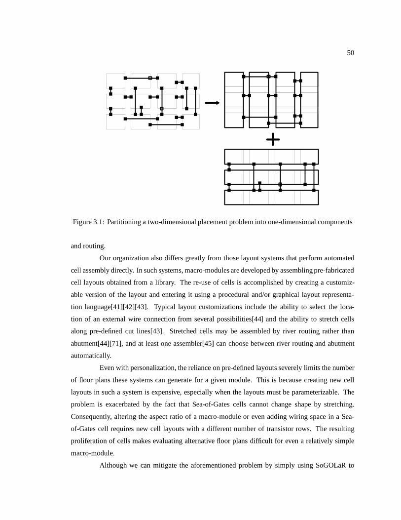
50
Figure 3.1: Partitioning a two-dimensional placement problem into one-dimensional components
and routing.
Our organization also differs greatly from those layout systems that perform automated
cell assembly directly. In such systems, macro-modules are developed by assembling pre-fabricated
cell layouts obtained from a library. The re-use of cells is accomplished by creating a customiz-
able version of the layout and entering it using a procedural and/or graphical layout representa-
tion language[41][42][43]. Typical layout customizations include the ability to select the loca-
tion of an external wire connection from several possibilities[44] and the ability to stretch cells
along pre-defined cut lines[43]. Stretched cells may be assembled by river routing rather than
abutment[44][71], and at least one assembler[45] can choose between river routing and abutment
automatically.
Even with personalization, the reliance on pre-defined layouts severely limits the number
of floor plans these systems can generate for a given module. This is because creating new cell
layouts in such a system is expensive, especially when the layouts must be parameterizable. The
problem is exacerbated by the fact that Sea-of-Gates cells cannot change shape by stretching.
Consequently, altering the aspect ratio of a macro-module or even adding wiring space in a Sea-
of-Gates cell requires new cell layouts with a different number of transistor rows. The resulting
proliferation of cells makes evaluating alternative floor plans difficult for even a relatively simple
macro-module.
Although we can mitigate the aforementioned problem by simply using SoGOLaR to
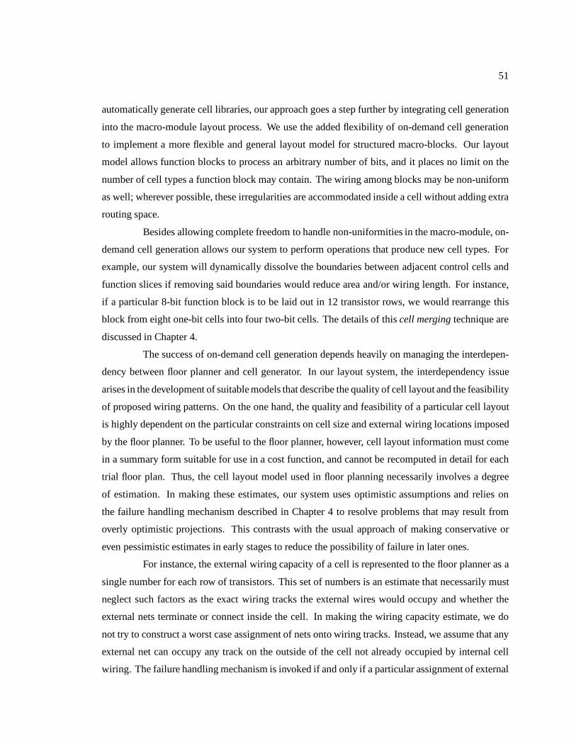
51
automatically generate cell libraries, our approach goes a step further by integrating cell generation
into the macro-module layout process. We use the added flexibility of on-demand cell generation
to implement a more flexible and general layout model for structured macro-blocks. Our layout
model allows function blocks to process an arbitrary number of bits, and it places no limit on the
number of cell types a function block may contain. The wiring among blocks may be non-uniform
as well; wherever possible, these irregularities are accommodated inside a cell without adding extra
routing space.
Besides allowing complete freedom to handle non-uniformities in the macro-module, on-
demand cell generation allows our system to perform operations that produce new cell types. For
example, our system will dynamically dissolve the boundaries between adjacent control cells and
function slices if removing said boundaries would reduce area and/or wiring length. For instance,
if a particular 8-bit function block is to be laid out in 12 transistor rows, we would rearrange this
block from eight one-bit cells into four two-bit cells. The details of this cell merging technique are
discussed in Chapter 4.
The success of on-demand cell generation depends heavily on managing the interdepen-
dency between floor planner and cell generator. In our layout system, the interdependency issue
arises in the development of suitable models that describe the quality of cell layout and the feasibility
of proposed wiring patterns. On the one hand, the quality and feasibility of a particular cell layout
is highly dependent on the particular constraints on cell size and external wiring locations imposed
by the floor planner. To be useful to the floor planner, however, cell layout information must come
in a summary form suitable for use in a cost function, and cannot be recomputed in detail for each
trial floor plan. Thus, the cell layout model used in floor planning necessarily involves a degree
of estimation. In making these estimates, our system uses optimistic assumptions and relies on
the failure handling mechanism described in Chapter 4 to resolve problems that may result from
overly optimistic projections. This contrasts with the usual approach of making conservative or
even pessimistic estimates in early stages to reduce the possibility of failure in later ones.
For instance, the external wiring capacity of a cell is represented to the floor planner as a
single number for each row of transistors. This set of numbers is an estimate that necessarily must
neglect such factors as the exact wiring tracks the external wires would occupy and whether the
external nets terminate or connect inside the cell. In making the wiring capacity estimate, we do
not try to construct a worst case assignment of nets onto wiring tracks. Instead, we assume that any
external net can occupy any track on the outside of the cell not already occupied by internal cell
wiring. The failure handling mechanism is invoked if and only if a particular assignment of external
52
nets to tracks fails to route. The section on floor planning describes in detail how cell layout metrics
are approximated and how these metrics are propagated up and down the macro-module hierarchy.
The rest of this chapter describes the implementation of our approach to macro-module
generation. Throughout the discussion below, we make comparative references to other datapath
layout systems, particularly those[72][73][74] that incorporate elements of general place and route
systems. Our discussion excludes those systems, such as SEFOP[73], where circuit structure
knowledge is incorporated in an indirect manner into a general place and route system, e.g., by
altering the weights of nets.
We begin with an overview of our layout model and task organization, then present
sections containing a detailed discussion of each task followed by a section with results. Although
our system relies on the failure handling and layout database services provided by the mediator, the
focus of this chapter is on floor planning and layout generation alone. The details of how cell layout
information is extracted from the design database and the details of the failure handling mechanism
are discussed in Chapter 4. Furthermore, we assume that all requests regarding cell layout to the
layout database are successful, i.e., no layout failures occur. Under this assumption, our system
runs in a stand-alone mode from start to finish.
3.1 Layout Model and Overview
Our system accepts input in the form of a structured hierarchical net-list. This hierarchical
structure may be given by the designer, or it may deduced from an annotated flat net-list by
clustering[75][76]. At the top level of such a net-list is a set of function slices to be placed side by
side in a row. The function slices may be grouped into hierarchies; creating such a group ensures
that the constituent function slices will be placed together with no other slices placed in between
them. Each function slice is composed of an array of cells to be placed in a column. Within a
function slice, we distinguish those cells that connect to cells in other function blocks to form a bit
slice. Borrowing from the terminology used in datapath design, we call such cells data cells, and
refer to cells that connect only to other cells in the same function slice as control cells. The latter
term is used because usually these are cells that generate signals to control the data cells in the
function slice. As the function slices themselves, the cells within a function slice may be grouped
into hierarchies. Since data cells in a function slice need not be uniform, hierarchies are used to
group instances of identical cells within a function slice. Figure 3.2 illustrates this organization.
We map the cells of each data cell block onto the Sea-of-Gates transistor array, by
53
Controlcells
0
1
2
3Data cell Data cell Data cell Data cell
Shifter ALU Mux
Function slices
BitSlices
Register file
BussesN-Diff.
P-Diff.Vdd
Vss
Metal 1
Metal 2
Figure 3.2: Floor Planning model for datapath generation showing function slices and theirconnectivity
stacking them perpendicular to the pre-fabricated diffusion strips. Data busses run in first level
metal parallel to the power supply lines, while second level metal is used for the control wiring
which runs primarily in the vertical direction. This orientation facilitates the alignment of data cells
and reduces the amount of wiring that must cross the power rails in second level metal.
This wiring model differs greatly from the more conventional row-based model for over-
the-cell wiring. This model, described by Tsujihashi et. al.[77], uses second layer metal for
power supply lines and data buses and first layer metal for control lines. Over the cell routing is
accomplished by implementing the “pin” that connects a cell to a data bus as a long vertical strap.
The strap provides a number of positions to attach a via to connect it to the horizontally running data
bus. The primary barrier is that this system relies on polysilicon jumpers to route short horizontal
nets and segments inside the cell. This option is not viable in Sea-of-Gates because the polysilicon
layer is pre-fabricated.
To process the input net-list, we have divided the task of macro-module synthesis into
three distinct steps, where each step is governed by a layout cost function expressed as a linear
combination of user scalable terms for wiring length, module width, module height and wiring
density. Although the layout cost function remains the same throughout layout synthesis, each
subsequent step uses its own method of estimating the value of each term, adding detail and
accuracy to the estimate until it reaches the the final actual layout cost. The resulting layout must

54
also satisfy user definable constraints on module height, width and the length of a set of nets.
To begin the process, we determine the aspect ratio of the module as well as the shape and
relative positions of its constituent function and bit slices. We call this step module floor planning
because our problem formulation is similar to that found in general purpose floor planning tools.
Within the module floor planner, the problem of optimizing the arrangement of a function slice
sequence is modeled as a linear placement problem with a multi-term objective function, with terms
for minimizing the length of busses between function slices, the number of busses passing through
each slice and the overall area of the macro-module.
The resulting function slice placement is then passed to the track assignment step, in
which the wires for external data busses are placed on specific outer tracks of the cell. Lastly, the
module assembly step performs the final layout synthesis of the macro-module. The actual module
layout is produced one cell at a time using SoGOLaR. The role of the module assembly step is to
propagate and pass to SoGOLaR the pin position constraints from the track assignment step and
from the adjacent cells whose layouts already have been completed.
All other regular macro-module layout systems that use the general place and route model
also use a task division similar to the one outlined above. This is despite the differences in routing
model and their use of stretchable library cells in lieu of cells generated on-demand. Because these
systems are distinguished only by the models and algorithms associated with the individual layout
tasks, all further comparative discussion is deferred to these sections.
3.2 Macro-Module Floor Planning
The module floor planner is so named because it determines the number of transistor rows
needed to implement each circuit block and assigns the relative positions of the blocks, thereby
producing a module floor plan suitable for external wiring and cell assembly. Although this task
statement is similar to that used by general purpose floor planners, our approach differs from these
in that we use the structure present in the input net-list to decompose the floor planning problem into
sub-tasks. We consider the problem of selecting the shape of the module and its constituent circuit
blocks separately from the problem of choosing the relative placement of the circuit blocks. In turn,
finding the relative placement of blocks is modeled as two separate one-dimensional sub-problems,
namely the ordering of function slices in a row and the ordering of bit slices in a column. This
approach is effective because most nets that connect among cells run entirely in one direction, either
vertically within a function slice or horizontally within a bit slice. The hierarchies are entirely
55
separate, thus those nets that cross both function and bit slices may be partitioned into horizontal
and vertical spans.
To find the minimum cost ordering of function or bit slices, the floor planner uses a branch
and bound[78] algorithm with the set of partial placements comprising the search tree. A partial
placement is a two-way partition of the input slices into an ordered set of placed slices and an
unordered set of unplaced slices. The algorithm generates new partial placements by moving one
slice from the unplaced set to the placed set2. These partial placements are kept in a queue ordered
by layout cost; the algorithm terminates when a complete placement appears at the head of this
queue.
This algorithm is attractive because it permits the easy inclusion of a variety of cost
function terms, the only restriction being that said term must increase monotonically as the partial
placement is constructed. In the absence of limiting constraints or heuristics, the algorithm will
generate partial placements from all parts of the search tree. Thus, it is guaranteed to return the
placement with the absolute minimum layout cost value. A comprehensive search would appear
impractical at first since the search tree contains O(n!) nodes for n slices. However, in practice the
search is limited by both lower and upper bounds to a tiny subset of the search tree. These desirable
features have led other layout system designers[72][79][74] to use the branch and bound algorithm
for function slice placement. Compared to ours, these systems solve a simpler placement problem
in that they assume the module shape as well as the vertical position and layout of each cell are
known before placement.
Our floor planner applies the branch and bound algorithm to each set of blocks in a
bottom-up pass through the net-list hierarchy. To reduce the complexity of this step, the initial
placement search computes costs for a single aspect ratio for the module selected before placement
begins. In selecting this aspect ratio, the floor planner takes into account the designer’s constraints,
cell layout feasibility and the amount of inter-cell wiring in each direction. Once a placement for
the module’s top level is found, the floor planner makes a top-down traversal to add the cost of
placement dependent factors, such as the cost of connecting external nets from inside the sub-block
to the correct location on the sub-block boundary. To obtain the lowest cost placement, the floor
planner must find and perform this computation on all placements whose pre-adjustment cost is less
than the post-adjustment cost of the original placement. This is accomplished by simply continuing
the branch and bound algorithm using the post-adjustment cost of the original placement as the upper
2w.l.o.g. the new slice is placed in the maximal (last) position of the placed set
56
bound. Concurrently, the floor planner uses a similar approach to expand the placement search to all
feasible aspect ratios. The details of these sub-tasks, floor planner initialization, placement search,
and placement adjustment are given in the next three sub-sections.
3.2.1 Initialization
To accurately compute the cost of placing a set of blocks, the floor planner must have the
dimensions, internal wiring cost and wiring capacity of each block. Thus, the floor planner must
have an estimate of the layout cost for each cell before it begins the initial placement search. These
costs are in turn dependent on the shape chosen for the module. We resolve this interdependency
by choosing a tentative module shape prior to block placement and then using the cell layouts
corresponding to the selected shape when computing costs during placement.
Since the floor planner eventually looks at all module shapes, we need not and in fact
cannot choose the aspect ratio that will correspond to the minimum cost floor plan. However, we
do minimize a lower bound estimate of the layout cost function in making our selection, and we
assign strong preference to module shapes that will produce aligned bit and function slices when
assembled. Satisfying the latter criterion is equivalent to choosing a single bit height for all cells in
the data block, where bit height is defined as Hb = R=B where R is the height in rows and B is the
number of bits processed.
The first step in this process, finding the range of feasible shapes for each cell, requires
only two queries to the layout database per cell. The queries seek the tallest and widest available cell
respectively and have no constraints specified. Specifying no constraints causes the layout database
to use already existing layouts to the maximum extent possible; no new cell layout will be generated
if any layout exists for the queried cell. Further details of how the layout database processes this
query are given in Chapter 4.
Given each cell’s range of feasible shapes, we use a bottom-up net-list traversal to find the
set of feasible bit heights for the data cell block. To begin, we define the set of feasible bit heights
for a cell as simply those values of Hb that lie in the range of feasible cell shapes and for which R
is an integer. Implicit in this calculation is the assumption that intermediate bit heights are always
implementable. In other words, we assume that if a cell can be implemented in one row per bit and
three rows per bit, then it can be implemented in two rows per bit as well.
In finding the feasible bit heights for a function slice, we admit the possibility that adjacent
cells with the same net-list may be merged. For example, two adjacent one-bit cells with the same
57
net-list may be merged into a single two-bit cell. This increases the number of feasible bit heights;
our example cell can now be implemented in three rows for two-bits. In doing this computation, we
assume that the representation of each function slice in the module net-list contains the least number
of bits per cell that is feasible. By this definition, an ALU comprised of eight 4-bit units may be
implemented as two 16-bit units but not as sixteen 2-bit units. To preserve the regularity expressed
in the net-list as much as possible, we restrict merging at this stage to cases where the merged
function slice would contain an integer number of cells. For instance, merging a function slice of n
one-bit cells into n=2 two-bit cells is allowed only if n is even.3. If cells with different net-lists are
in the same function slice, the merger must be feasible for each group of cells individually.
The next step in choosing a module shape is to choose a feasible bit height from the group
of feasible bit height sets produced previously. For purposes of this calculation, each group of cells
with the same net-list and in the same function slice has its own set of feasible bit heights. As
mentioned previously, in finding the shape of the data block, we want to use the bit height most
likely to allow all bit slices in the module to be aligned. This amounts to finding the bit height that
is a member of the greatest number of feasible height sets.
Our objective is therefore to choose the bit height with greatest cardinality that meets the
input constraints on layout cost. If more than one bit height with the same cardinality meets the
input constraints, we choose the one with smallest layout cost. The lower bound for module height
and width is found by summing the height of the bit slices and the width of all function slices, where
the dimension of function and bit slices are determined by the tallest and widest cells respectively.
Here we make the optimistic assumption that all cells will be tightly packed in the sense that all
cells in the data block will have the chosen bit height and all control cells will be no wider than the
data cells in their function slice. Module height may be computed directly because in Sea-of-Gates
transistor row height is fixed. Our estimate of the width of a cell in a bit height not already obtained
from the database is an extrapolation based on the number of transistors and the number of templates
in the cell(s) that were found in the range-finding step. Using this extrapolation reduces the number
of queries made to the layout database. Extrapolating beyond the range of bit heights for a cell is
justified by the fact that the given range only includes bit heights already in the database, not all
possible bit heights for a cell.
Because of the difficulty of making an accurate estimate of bus capacity without consulting
the layout database, we don’t consider the density component of layout cost in this step. The net-
3A method for implementing merge that produce odd “left over” cells is given in Chapter 4
58
length computation for external nets will produce only nominal values except for those nets that
connect between fixed positions on the boundary of the module and those nets that connect to most
or all cells in the data block. The latter case occurs with nets that carry control signals to cells in
the data block.
Before proceeding with the initial placement search, we update the layout cost for each
cell in the chosen bit height. For data block cells, we query the database using the chosen bit height
as a constraint; control cells are constrained to the width of the data cells in their function slice. With
these constraints, the layout database will create a cell to meet constraints if none already exists
and will report a failure if said cell cannot be created. If a data cell cannot be created, we simply
choose the next best bit height and begin again. Control cell failures are handled by widening the
containing function slice and adjusting the module cost estimate accordingly. The floor planner will
proceed as long as a single bit-height is found for all data cells and the adjusted cost does not exceed
the input constraints. Otherwise, the floor plan is sent to the failure handler described in Chapter 4.
3.2.2 Initial Placement Search
As mentioned previously, finding the relative placement of blocks is modeled as two
separate one-dimensional problems, namely the ordering of function slices in a row and the ordering
of bit slices in a column. The initial placement search consists of two bottom-up passes through the
net-list hierarchy to find a relative placement for each set of function and bit slices independently
using the branch and bound algorithm. The search is referred to as initial in part because all layout
cost calculations are based on the module shape chosen previously. Furthermore, using a bottom-up
traversal means that pin position information derived from placing a block is not propagated to
the sub-blocks. Although the placements found in this step may no longer have lowest cost when
the simplifying assumptions are relaxed, the placement adjustment step uses the ordered queue of
partial placements to ensure that only a few promising candidates use the expensive final placement
cost evaluation. Since the bulk of unpromising placements are rejected as quickly as possible,
partitioning the floor planning task reduces the overall execution time even though slightly more
partial placements are evaluated.
In our context, the branch and bound algorithm[78] is an ordered traversal of the set of
partial placements Q for the given set of blocksB = b1; :::bn. Each partial placement is an ordered
pair (p; cp) where p is an ordered subset of k blocks bl1; :::bmk for k = 1:::n and cp is the layout
cost for partial placement p. Each p forms a two-way partition of the set of blocks into placed and
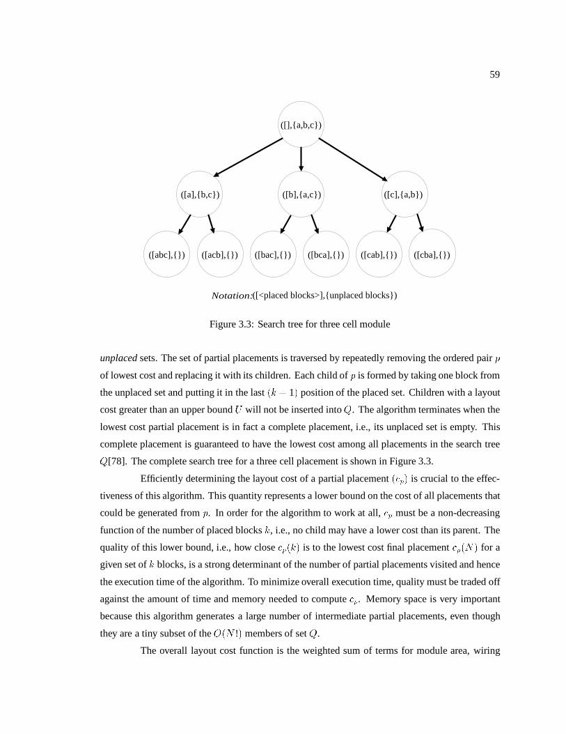
59
([],{a,b,c})
([b],{a,c}) ([c],{a,b})
([abc],{}) ([acb],{}) ([bac],{}) ([bca],{}) ([cab],{}) ([cba],{})
([a],{b,c})
Notation:([<placed blocks>],{unplaced blocks})
Figure 3.3: Search tree for three cell module
unplaced sets. The set of partial placements is traversed by repeatedly removing the ordered pair p
of lowest cost and replacing it with its children. Each child of p is formed by taking one block from
the unplaced set and putting it in the last (k + 1) position of the placed set. Children with a layout
cost greater than an upper bound U will not be inserted into Q. The algorithm terminates when the
lowest cost partial placement is in fact a complete placement, i.e., its unplaced set is empty. This
complete placement is guaranteed to have the lowest cost among all placements in the search tree
Q[78]. The complete search tree for a three cell placement is shown in Figure 3.3.
Efficiently determining the layout cost of a partial placement (cp) is crucial to the effec-
tiveness of this algorithm. This quantity represents a lower bound on the cost of all placements that
could be generated from p. In order for the algorithm to work at all, cp must be a non-decreasing
function of the number of placed blocks k, i.e., no child may have a lower cost than its parent. The
quality of this lower bound, i.e., how close cp(k) is to the lowest cost final placement cp(N) for a
given set of k blocks, is a strong determinant of the number of partial placements visited and hence
the execution time of the algorithm. To minimize overall execution time, quality must be traded off
against the amount of time and memory needed to compute cp. Memory space is very important
because this algorithm generates a large number of intermediate partial placements, even though
they are a tiny subset of the O(N !) members of set Q.
The overall layout cost function is the weighted sum of terms for module area, wiring
60
length, and wiring density respectively. The module shape is fixed at this stage, thus all partial
placements have the same area and thus the effective cost function is the weighted sum of wiring
length and density. Since each level of hierarchy is placed independently, we consider only those
portions of nets connecting to the sub-blocks at the current level. Pins on a sub-block are represented
by the left- and right-most position where a connection may be made. All external connections are
represented by a single pin, hence we refer to the connected interval of a pin or block interchangeably.
Of the two cost components, the algorithm for finding wiring length is the most involved.
We begin by computing a lower bound on the length of each net for a partial placement of zero
blocks. For each block connected to the net, we first find the minimum internal span for the
net, defined as ds = min(dl; dr) where dl and dr are the distance from the left/right edges of the
connected interval to the left/right edges of the block, respectively. We then sort these blocks using
the quantityBwi� dsi, this being the difference of the width of block Bi and its minimum internal
span. We call this the effective size of the block, or simply size if the context is clear. The lower
bound length for a net may be found by summing the sizes of all connected blocks except the two
largest ones. This corresponds to the case where the two largest blocks define the left and right edge
of the net’s span.
To increase the quality of the lower bound cost estimate, updates to each net’s length are
made incrementally as soon as the amount of the increase is known. Updates are handled separately
depending on whether the block currently being moved to the placed set is connected to the given
net or not. Each time an unconnected block is placed in the span of the net, we add the width of
that block to the net’s length. Ordinarily, the net’s span extends from the right edge of the first
connected block to the left edge of the last. This may change if the net has pins whose position is
fixed; these include pins external to the module’s top level as well as pins on fixed blocks. Such
pins are modeled by an ordered pair (xl; xr) where the pin may be placed in the interval from xl to
xr. For fixed blocks, xl and xr correspond to the left and right edge of the block respectively. We
define the left and right extent of a net with n fixed pins as max(xl1; :::xln) and min(xr1; :::xrn),
this being the rightmost left edge and leftmost right edge of each interval, respectively. The span of
the net is increased if its right extent is left of the first non-fixed pin or its left extent is to the right
of the last non-fixed pin.
Each time we encounter a block connected to the net, we increase the lower bound net
length found before placement according to the algorithm whose pseudo-code description is given
below.
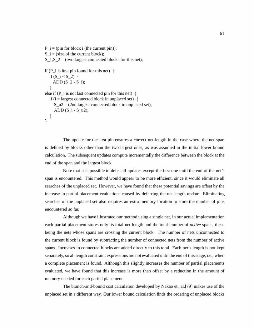
61
P_i = (pin for block i (the current pin));S_i = (size of the current block);S_1,S_2 = (two largest connected blocks for this net);
if (P_i is first pin found for this net) f
if (S_i < S_2) fADD (S_2 - S_i);
g
else if (P_i is not last connected pin for this net) fif (i = largest connected block in unplaced set) f
S_u2 = (2nd largest connected block in unplaced set);ADD (S_i - S_u2);
gg
The update for the first pin ensures a correct net-length in the case where the net span
is defined by blocks other than the two largest ones, as was assumed in the initial lower bound
calculation. The subsequent updates compute incrementally the difference between the block at the
end of the span and the largest block.
Note that it is possible to defer all updates except the first one until the end of the net’s
span is encountered. This method would appear to be more efficient, since it would eliminate all
searches of the unplaced set. However, we have found that these potential savings are offset by the
increase in partial placement evaluations caused by deferring the net-length update. Eliminating
searches of the unplaced set also requires an extra memory location to store the number of pins
encountered so far.
Although we have illustrated our method using a single net, in our actual implementation
each partial placement stores only its total net-length and the total number of active spans, these
being the nets whose spans are crossing the current block. The number of nets unconnected to
the current block is found by subtracting the number of connected nets from the number of active
spans. Increases in connected blocks are added directly to this total. Each net’s length is not kept
separately, so all length constraint expressions are not evaluated until the end of this stage, i.e., when
a complete placement is found. Although this slightly increases the number of partial placements
evaluated, we have found that this increase is more than offset by a reduction in the amount of
memory needed for each partial placement.
The branch-and-bound cost calculation developed by Nakao et. al.[79] makes use of the
unplaced set in a different way. Our lower bound calculation finds the ordering of unplaced blocks

62
that minimizes the length of each net independently. In fact, using the order that minimizes one
net’s cost may preclude the minimization of other nets. In their method, this interaction is taken
into account when checking delay constraints (bounds on the total length of a subset of nets). A
partial placement will be excluded from further expansion if no ordering of blocks in the unplaced
set can satisfy all delay constraints. Compared to our method, this approach will produce fewer
node evaluations. However, the algorithm has a very high order of complexity in the number of
delay constraints.
The number of active spans also forms a component of the wiring density cost. The total
wiring density at block k is the sum of the number of active spans and its internal density dk, this
being the density of wiring entirely inside the block. The internal density of the current block is the
density of the final complete placement with all nets that connect outside the block removed. The
density component used by our cost function is simply the maximum total density over all blocks.
The wiring capacity of each function slice is also computed and propagated up the net-list
hierarchy in this step, but we do not exclude partial placements that exceed this capacity. This is
because the wiring capacity in a given direction changes dramatically with module aspect ratio, thus
the same placement in a different module shape may satisfy this constraint.
Although we have illustrated our algorithms in terms of placing function slices in a row,our
algorithm is used first to order bit slices in a column. We are able to speed up this step dramatically
by exploiting the characteristics of bit slice connections. Specifically, when constructing partial
placements we never place two disconnected bit slices adjacent to each other. Cai et. al.[72]
illustrated that this heuristic can speed up the placement of large numbers of function slices. We
have found its importance to bit slice placement to be very great, since many connections among bit
slices are made between pairs of bit slices; shifters and carry propagate adders are examples of this.
In many datapaths these connections run between the same pair of bits in all function slices, hence
we may eliminate a huge number of partial placements by restricting adjacency to these connected
pairs. Although the number of bit slices often exceeds the number of function slices, in no case
have we found that bit slice placement makes a significant contribution to floor planner execution
time.
3.2.3 Placement Adjustment
Although the ordering of blocks output by the initial placement stage constitutes a com-
plete floor plan, several elements of layout optimization have been neglected in order to find this
63
candidate floor plan more efficiently. The missing elements may be grouped into the following
three categories:
Module Shape The initial module shape was chosen based on a cost estimate found by interpolating
between the smallest and largest data block aspect ratios for which cells could be generated.
Thus, the feasibility of the chosen module shape and its dimensions relative to other shapes
are not known until cells have been instantiated for it. The dimensions and wiring capacity
of the new cell instances may differ from the old ones, thus we alter the wiring cost of the
candidate floor plan as well.
External Pin Placement The layout of any set of blocks below the top level of net-list hierarchy
does not take into account the positioning of connections from higher level blocks. Conse-
quently, we neglect the cost of connecting a higher level net to its sub-blocks to ensure that
the calculated wiring length and density remains a lower bound.
Constraint Checking Net-length and wiring density constraints are not checked in the initial stage
since these costs are strongly dependent on both module shape and the cost of connections to
sub-blocks.
Each of these elements may either eliminate our initial complete floor plan or cause an
alternate floor plan to have lower cost. Thus, this stage must find and perform the placement
adjustments on each viable alternative before selecting the final floor plan.
We model the search for alternative floor plans as a continuation of the branch and bound
search described previously. Whenever an adjustment to the layout cost is performed, we find an
upper bound on the increase in layout cost that can result from the adjustment. We then use the
initial placement search algorithm to evaluate all partial placements whose total cost is currently
less than the given bound. Partial placements are evaluated as in the initial stage, and all completed
placements are stored in a separate completed placement list. This list comprises all of the candidates
for lowest cost floor plan, however the lowest cost floor plan is not known until all adjustments have
been made. This incremental search is at the core of all placement adjustments made in this stage.
In the first placement adjustment, every member of the completed placement list receives
a top-down pass that reorders each of the sub-blocks using the external pin position derived from
the top level placement. This reordering is much more expensive than the sub-block placement in
the initial placement stage, hence the need for good upper bounds when generating the completed
placement list. We then illustrate how the above adjustment is used in the search of different module
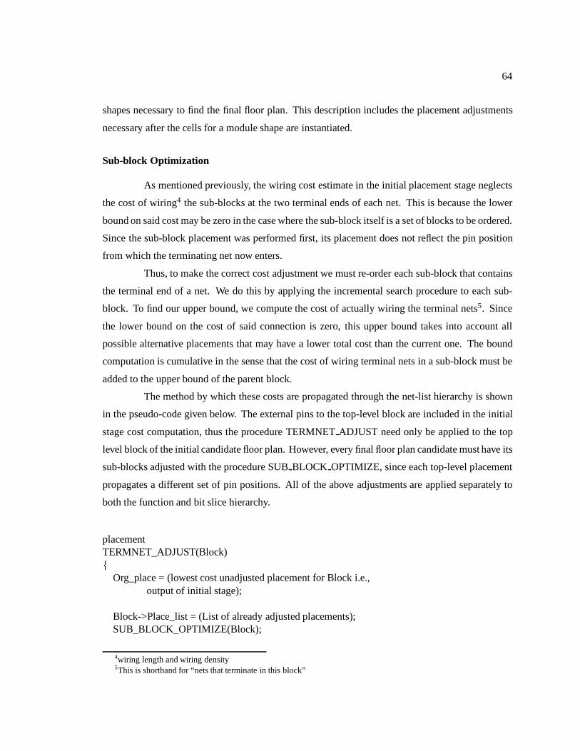
64
shapes necessary to find the final floor plan. This description includes the placement adjustments
necessary after the cells for a module shape are instantiated.
Sub-block Optimization
As mentioned previously, the wiring cost estimate in the initial placement stage neglects
the cost of wiring4 the sub-blocks at the two terminal ends of each net. This is because the lower
bound on said cost may be zero in the case where the sub-block itself is a set of blocks to be ordered.
Since the sub-block placement was performed first, its placement does not reflect the pin position
from which the terminating net now enters.
Thus, to make the correct cost adjustment we must re-order each sub-block that contains
the terminal end of a net. We do this by applying the incremental search procedure to each sub-
block. To find our upper bound, we compute the cost of actually wiring the terminal nets5. Since
the lower bound on the cost of said connection is zero, this upper bound takes into account all
possible alternative placements that may have a lower total cost than the current one. The bound
computation is cumulative in the sense that the cost of wiring terminal nets in a sub-block must be
added to the upper bound of the parent block.
The method by which these costs are propagated through the net-list hierarchy is shown
in the pseudo-code given below. The external pins to the top-level block are included in the initial
stage cost computation, thus the procedure TERMNET ADJUST need only be applied to the top
level block of the initial candidate floor plan. However, every final floor plan candidate must have its
sub-blocks adjusted with the procedure SUB BLOCK OPTIMIZE, since each top-level placement
propagates a different set of pin positions. All of the above adjustments are applied separately to
both the function and bit slice hierarchy.
placementTERMNET_ADJUST(Block)f
Org_place = (lowest cost unadjusted placement for Block i.e.,output of initial stage);
Block->Place_list = (List of already adjusted placements);SUB_BLOCK_OPTIMIZE(Block);
4wiring length and wiring density5This is shorthand for “nets that terminate in this block”
65
Tmp_list = NULL;if ((Placement of Block not fixed)) f
Bound = WIRING_COST(Org_place);for((Each Sub_block of Block)) f
Bound += (Cost of terminating external netsin Sub_block);
g
Tmp_list = SEARCH_FORWARD(Bound);for((Each Element in Tmp_list)) f
SUB_BLOCK_OPTIMIZE(Element);g
g
Block->Place_list = UNION(Place_list,Tmp_list);return(MINCOST_ELEMENT(Place_list);
g
voidSUB_BLOCK_OPTIMIZE(Block)f
for(Each Sub_block of Block) f(Propagate external pin positions to Sub_block);TERMNET_ADJUST(Sub_block);
g
g
Choosing The Final Floor Plan
Although the adjustment for terminating nets must be applied to each placement, it is but
a small part of the search for the final floor plan. This search is structured as the selection and
evaluation of candidate module shapes drawn from the list of feasible module shapes developed
prior to placement. To accurately compute the cost of a candidate module shape, every cell in
the module must be re-instantiated using the bit height corresponding to that module shape. This
process forms the core of the final floor plan selection routine, and we use the phrase “instantiating
the module shape” as a shorthand label for it.
The selection of module shapes for instantiation is partly governed by the estimated layout
cost found in the initial module shape stage. We augment our previous cost estimation with the
appropriately scaled wiring cost of the lowest cost function and bit slice placement. The new cost
element will skew the shape selection in favor of taller or shorter module shapes depending on
66
whether the wiring cost is greatest in the horizontal or vertical direction.
Our other objective in module shape selection is to avoid instantiating a shape that has a
low probability of meeting the user defined constraints, even if said shape has the lowest estimated
cost. Module shapes are represented by their bit height, previously defined as the number of rows
divided by the number of bits. We therefore may immediately exclude any shape that is outside
the specified bounds. Our estimates for all other metrics are not necessarily lower bounds, thus a
constraint that is violated here may in fact be satisfied after instantiation.6 To assist in making the
possible tradeoff between cost and likelihood of success, we compute for each constraint shape the
degree to which each constraint is violated. These amounts are expressed as a percentage of the
value of the underlying metric. For example, if the total wiring length of a module were 2000 and
a net exceeded its length constraint by 40, said excess would be counted as two percent. Summing
all percentages yields a rough idea of the degree to which constraints are violated for a prospective
shape. All possible shapes above a threshold of five percent are ordered separately and will be
instantiated only if all shapes below five percent are exhausted.
Instantiating a module shape alters the width, wiring length, and wiring capacity of each
cell. Since we have not customized the external pins of each cell7, cell wiring length only affects
the cost of the current shape relative to others. As was the case with selecting module shape, we
apply constraint tests (e.g., cell wiring capacity) only after having found the lowest cost placement
for the instantiated module shape. This leaves changes in cell width as the only factor that directly
affects the cost of each function slice placement. Furthermore, only relative width changes among
slices can affect the ordering of the completed placement list.
To find the bound for the cell width placement adjustment, we must first proportionally
scale each function slice in the lowest cost placement to the actual (instantiated) module width.
For each function slice i, we then compute Ri = wiA=wiE, this being the ratio of the actual to the
normalized estimated width. Thus the maximum possible decrease in wiring length that may result
from width adjustment is given by ∆NL = (1 � Rmin(i)) �NLE, where Rmin(i) is the minimum
ratio for all function slices, and NLE is the total wiring length of the normalized uninstantiated
module. This corresponds to the case in which all wires run over slices that shrink the most relative
to all other slices in the module. Given the adjusted wiring length of the (currently) lowest cost
placementNLA, all placements with adjusted length less thanNLA must have an unadjusted length
no greater than NLA + ∆NL.
6Lower bounds are computable, but we have found them so rarely useful that they aren’t included here.7We have found the wiring model currently in effect too crude for this purpose.
67
The pseudo-code description given below shows how all of the placement adjustments
are integrated into a search for the lowest cost floor plan. The routine WIDTH ADJUST applies the
adjustment described above to each group in the function slice hierarchy. This routine is analogous to
the terminal net adjustment procedure TERMNET ADJUST outlined earlier. Each new placement
produced this way must have the terminal nets of its sub-blocks adjusted, hence the calls to routine
SUB BLOCK OPTIMIZE. Finally, note that each subsequent application of the width adjustment
routine will add to the list of completed placements only if the bound for that iteration exceeds the
cost of all completed placements found so far.
/* Find the final floor plan or NULL if can’t meet constraints. */floor_planFIND_FPLAN(Top_Block)f
TERMNET_ADJUST(Top_Block,FUNCTION_SLICES);TERMNET_ADJUST(Top_Block,BIT_SLICES);Shape_list = (List of eligible module shapes sorted by
estimated cost, including theadjusted wiring cost of Top_Block);
Min_fplan = NULL;do f
Min_shape = MINCOST_ELEMENT(Shape_list);Min_shapebound = INSTANTIATE_SHAPE(Top_Block,Min_Shape);
Tmp_list = WIDTH_ADJUST(Top_Block,Min_shapebound);for((Each Element in Tmp_list)) f
SUB_BLOCK_OPTIMIZE(Element);gTop_Block->Place_list = UNION(Top_Block->Place_list,
Tmp_list);REMOVE_ELEMENT(Shape_list,Min_shape);
Tmp_Fplan = FIND_MINFPLAN(Top_Block->Place_list);if ((Min_Fplan == NULL) || (Tmp_fplan < Min_fplan)) f
Min_fplan = Tmp_fplan;g
while(Min_fplan > MINCOST_ELEMENT(Shape_list));
return(Min_fplan);g
The procedure FIND MINFPLAN searches the completed placement list for the lowest
68
cost placement for the given shape that meets constraints. If the lowest cost placement currently
does not meet constraints, we discard it unless only wiring capacity constraints are violated. In
this case, we first try to correct the failure by re-instantiating the offending cell(s) with the required
wiring capacity as a constraint. The candidate placement is kept only if the new cells remove all
violations without introducing any new ones, otherwise the placement must be discarded. Under
the current area calculation model, all placements for a given shape have the same width. Thus, a
width constraint violation terminates any further processing using the current module shape.
With each module shape instantiation we also update our cost estimates for all uninstan-
tiated module shapes. Recall that our estimation method amounts to a linear interpolation for all
shapes whose bit height lies in between the instantiated shapes. Adding a new instance partitions
the regions into two segments, said regions are adjusted accordingly.
Exploration halts when all eligible module shapes have been explored or when the cost of
the best floor plan is less than the best cost of any uninstantiated module shape. Finally, the failure
handler will be invoked if all eligible shapes are explored and no floor plan that meets constraints
has been found. Otherwise, the chosen floor plan is returned as the final output of the floor planning
phase.
3.3 Routing and Module Assembly
Our approach to completing the module layout is similar to the floor planning step in that
we try to use cell and interconnect regularity to develop a wiring model that is more efficient than
its general macro-cell counterpart. In particular, our objective is to maximize the amount of wiring
that can be routed over the Sea-of-Gates cells. This objective is critical in Sea-of-Gates because
extra routing space may be obtained only by adding an empty row or column of transistors at a great
increase in both area and wiring cost.
To achieve this objective, we try to perform as much routing as possible by applying
appropriate constraints to the external pins of the cell when generating its final layout. This allows
us to complete the wiring of nets between cells by abutting matching pins while assembling said
cells to form the final layout of the module. By applying different kinds of constraints, this
mechanism can handle connections among instances of identical cells in a function slice array as
well as connections to two adjacent arrays of different cell types.
The primary difficulty of routing a net by pin constraint propagation is that the exact
location of its wiring is determined by the first cell layout that is instantiated. In the case of long
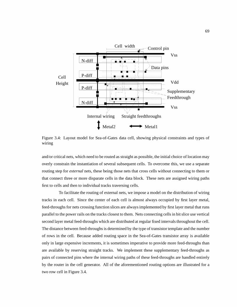
69
P-diff
P-diff
N-diff
N-diff
Cell width
Vss
Vss
Vdd
Control pin
Internal wiring
CellHeight
Metal1Metal2
Straight feedthroughs
Data pins
SupplementaryFeedthrough
Figure 3.4: Layout model for Sea-of-Gates data cell, showing physical constraints and types ofwiring
and/or critical nets, which need to be routed as straight as possible, the initial choice of location may
overly constrain the instantiation of several subsequent cells. To overcome this, we use a separate
routing step for external nets, these being those nets that cross cells without connecting to them or
that connect three or more disparate cells in the data block. These nets are assigned wiring paths
first to cells and then to individual tracks traversing cells.
To facilitate the routing of external nets, we impose a model on the distribution of wiring
tracks in each cell. Since the center of each cell is almost always occupied by first layer metal,
feed-throughs for nets crossing function slices are always implemented by first layer metal that runs
parallel to the power rails on the tracks closest to them. Nets connecting cells in bit slice use vertical
second layer metal feed-throughs which are distributed at regular fixed intervals throughout the cell.
The distance between feed-throughs is determined by the type of transistor template and the number
of rows in the cell. Because added routing space in the Sea-of-Gates transistor array is available
only in large expensive increments, it is sometimes imperative to provide more feed-throughs than
are available by reserving straight tracks. We implement these supplementary feed-throughs as
pairs of connected pins where the internal wiring paths of these feed-throughs are handled entirely
by the router in the cell generator. All of the aforementioned routing options are illustrated for a
two row cell in Figure 3.4.
70
Our approach to routing external nets borrows from algorithms developed for general
row-based routers. For instance, in the first routing phase, the array of cells and their feed-through
capacities are modeled with a global routing grid graph[22]. This allows us to borrow from a variety
of approaches originally developed for the global routing of standard cell rows. Similarly, wiring
tracks are allocated using a model analogous to that for channel routing[29]. The details of our
algorithms for routing and module assembly are given in the following three sub-sections.
3.3.1 Global Routing
Unlike the floor planner, the routing stage operates on the “flat” version of the input
net-list. Thus the only objects present at the input are cells and their interconnecting nets. We
assume that each cell at the input is annotated with its location and size as well as its wiring capacity
in each orientation (horizontal and vertical). We also assume that all cells are rectangular and none
overlap. Although some pins were assigned to sides of the cell during floor planning, we do not
explicitly use these assignments during routing.
To begin, we map the annotated net-list into our global routing graph. This graph is based
on the familiar grid graph[22] model where nodes represent cells and links represent the wiring
capacity between two cells. A separate link is used for each pair of cells that share a boundary,
hence each cell’s side may require more than one link. Since all cells are rectangular, each link is
associated with an orientation (horizontal or vertical), and a side of the cell (top, bottom, left, right).
Empty space between cells is not assigned a separate node, instead links are projected across the
space to the cell boundary on the opposite side.
The wiring capacity figures for each cell represent the number of wires that may pass
through the cell in each orientation. The figure for a given orientation is assigned to the two sides
with that orientation as the sum of the boundary edge capacities for that side. For example, if cell
A has a vertical feed-through capacity of four, then the sum of all links that cross the top side of
cell A would be four, as would the sum of all links that cross the bottom side. Each link on a side
is assigned the fraction of the capacity roughly equal to the fraction of that side’s length occupied
by its boundary. This apportionment is done for both cells on the boundary, with the link receiving
the minimum of that pair of values.
This assignment is adjusted when a cell’s side has several links, one of which connects
to a cell with very low capacity. An apportionment based strictly on boundary length may result
in some capacity going unused. In this case, the unused capacity may be reassigned to another
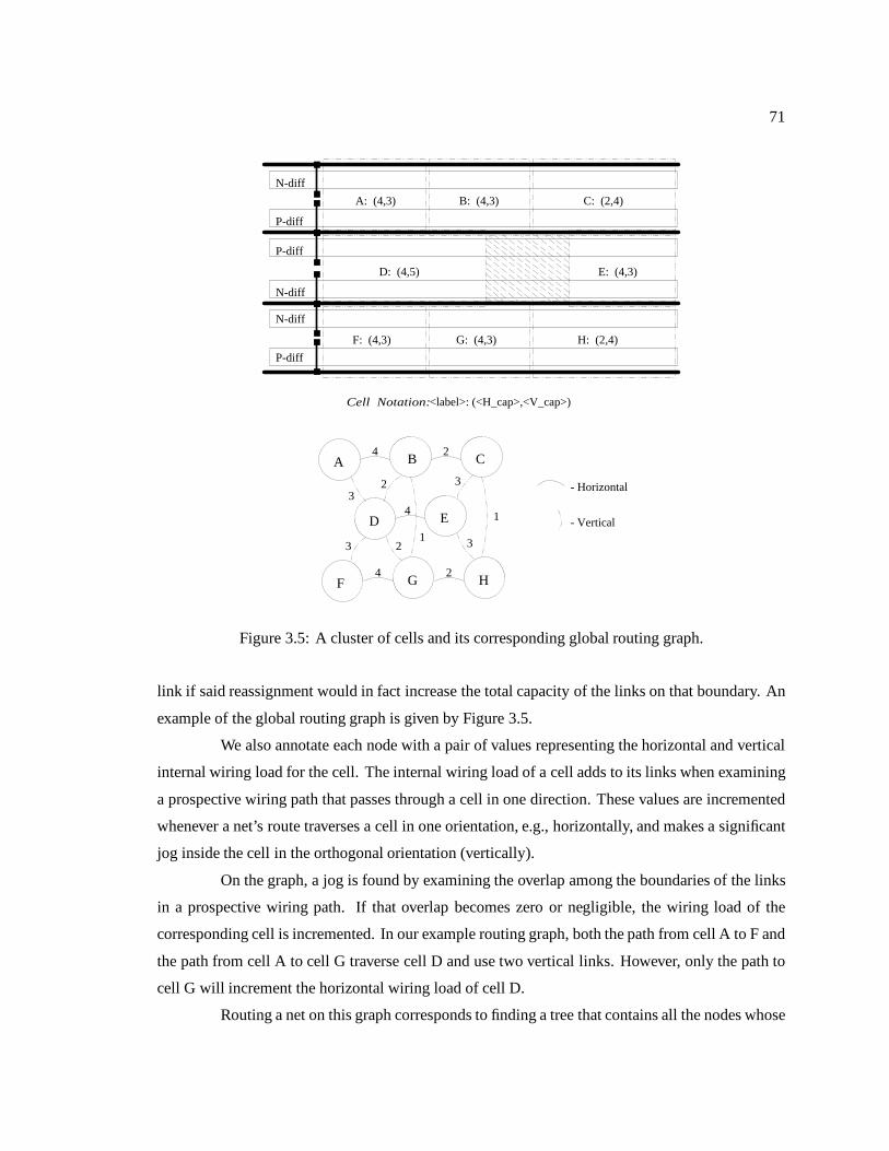
71
P-diff
P-diff
N-diff
P-diff
N-diff
N-diff
A: (4,3) B: (4,3)
G: (4,3)F: (4,3)
E: (4,3)D: (4,5)
C: (2,4)
H: (2,4)
<label>: (<H_cap>,<V_cap>)Cell Notation:
A B C
E
HGF
D
- Horizontal
- Vertical
2
2
4
3
31
1
3
3
4
4 2
2
Figure 3.5: A cluster of cells and its corresponding global routing graph.
link if said reassignment would in fact increase the total capacity of the links on that boundary. An
example of the global routing graph is given by Figure 3.5.
We also annotate each node with a pair of values representing the horizontal and vertical
internal wiring load for the cell. The internal wiring load of a cell adds to its links when examining
a prospective wiring path that passes through a cell in one direction. These values are incremented
whenever a net’s route traverses a cell in one orientation, e.g., horizontally, and makes a significant
jog inside the cell in the orthogonal orientation (vertically).
On the graph, a jog is found by examining the overlap among the boundaries of the links
in a prospective wiring path. If that overlap becomes zero or negligible, the wiring load of the
corresponding cell is incremented. In our example routing graph, both the path from cell A to F and
the path from cell A to cell G traverse cell D and use two vertical links. However, only the path to
cell G will increment the horizontal wiring load of cell D.
Routing a net on this graph corresponds to finding a tree that contains all the nodes whose
72
cells contain connections to the net. Our objective is to find minimum cost trees for each net subject
to the constraints on link capacity. Our cost measure is the length of all cells and blank tiles traversed
by the net. The method used to compute this value on the graph depends on the orientation of the
net’s entering and exiting links. If the orientations are the same, all of the wiring length is considered
to be in that orientation (horizontal or vertical) and we use the cell’s height or width respectively.
When a net turns a corner in a cell, the link orientations differ and we must sum the horizontal and
vertical net-length components. Here we use the distance between the boundary of one edge and
the midpoint value of the opposite edge. To aid these calculations, all links are annotated with the
location of midpoint of the boundary they cross. The boundary midpoints are also used to find the
length in the orthogonal direction when a wire makes a significant jump inside the cell. Finally,
links that cross blank space are marked with the distance between the two boundaries.
In graph theoretic terms, the tree representing a net’s route is called a Steiner tree, and the
problem of finding minimum cost Steiner trees is known to be NP-complete[14]. Our approach to
this problem begins by constructing low cost trees one at a time for each net. Since each net’s routing
reduces the capacity of some graph links, nets that are routed later encounter a more constrained
graph than do nets routed earlier. Thus, the final cost of all nets is strongly dependent on the order
in which nets are processed. This is the primary difficulty with our chosen approach.
Our strategy to overcome this difficulty is to identify special cases for which the minimum
cost tree may be found directly and route those nets first. The most important special case for regular
modules are nets which may be routed in a “straight line” path. This occurs when the net lies entirely
in one bit or function slice. Instead of trying to identify these nets before routing them, we simply
attempt to route every net by a straight line construction. Specifically, we attempt to construct a
path from left to right (bottom to top) using only links of horizontal (vertical) orientation without
backtracking, i.e., always entering and exiting a cell on opposite sides. A path is successful if all
nodes with pins can be reached from the starting node in this manner. If only one pin node cannot
be reached, we attempt to find a straight line path from that node to any node on the main path. If
that construction is successful, the resulting “T” path is the minimum value route for that net.
At this point, the remaining nets have a pin configuration for which the straight line or
“T” path is not necessarily minimal. These nets are handed to an algorithm for generating low
cost Steiner trees with arbitrary pin configurations. We use the method, first outlined by Ho et.
al.[80], which works by first constructing a minimum cost spanning tree (abbreviated MST) for
the net and then converting each link of the MST into a path in the original routing graph. The
spanning tree must be separable in the sense that deleting an link from the MST results in sub-
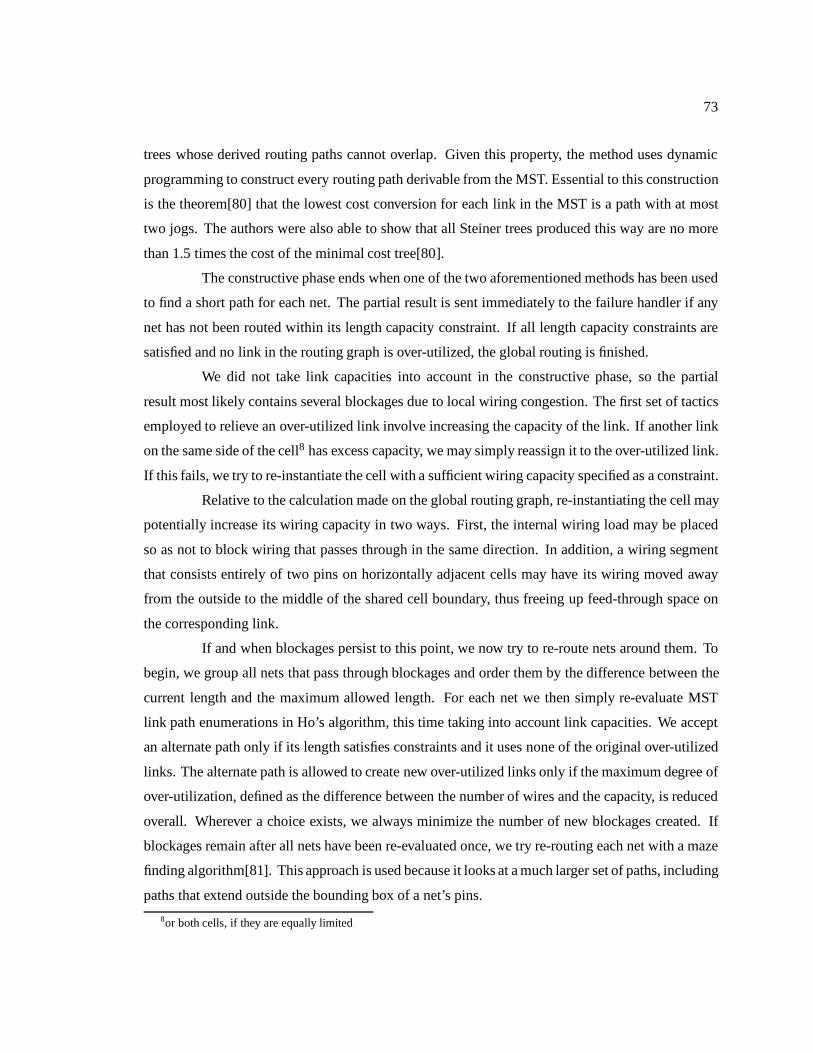
73
trees whose derived routing paths cannot overlap. Given this property, the method uses dynamic
programming to construct every routing path derivable from the MST. Essential to this construction
is the theorem[80] that the lowest cost conversion for each link in the MST is a path with at most
two jogs. The authors were also able to show that all Steiner trees produced this way are no more
than 1.5 times the cost of the minimal cost tree[80].
The constructive phase ends when one of the two aforementioned methods has been used
to find a short path for each net. The partial result is sent immediately to the failure handler if any
net has not been routed within its length capacity constraint. If all length capacity constraints are
satisfied and no link in the routing graph is over-utilized, the global routing is finished.
We did not take link capacities into account in the constructive phase, so the partial
result most likely contains several blockages due to local wiring congestion. The first set of tactics
employed to relieve an over-utilized link involve increasing the capacity of the link. If another link
on the same side of the cell8 has excess capacity, we may simply reassign it to the over-utilized link.
If this fails, we try to re-instantiate the cell with a sufficient wiring capacity specified as a constraint.
Relative to the calculation made on the global routing graph, re-instantiating the cell may
potentially increase its wiring capacity in two ways. First, the internal wiring load may be placed
so as not to block wiring that passes through in the same direction. In addition, a wiring segment
that consists entirely of two pins on horizontally adjacent cells may have its wiring moved away
from the outside to the middle of the shared cell boundary, thus freeing up feed-through space on
the corresponding link.
If and when blockages persist to this point, we now try to re-route nets around them. To
begin, we group all nets that pass through blockages and order them by the difference between the
current length and the maximum allowed length. For each net we then simply re-evaluate MST
link path enumerations in Ho’s algorithm, this time taking into account link capacities. We accept
an alternate path only if its length satisfies constraints and it uses none of the original over-utilized
links. The alternate path is allowed to create new over-utilized links only if the maximum degree of
over-utilization, defined as the difference between the number of wires and the capacity, is reduced
overall. Wherever a choice exists, we always minimize the number of new blockages created. If
blockages remain after all nets have been re-evaluated once, we try re-routing each net with a maze
finding algorithm[81]. This approach is used because it looks at a much larger set of paths, including
paths that extend outside the bounding box of a net’s pins.
8or both cells, if they are equally limited
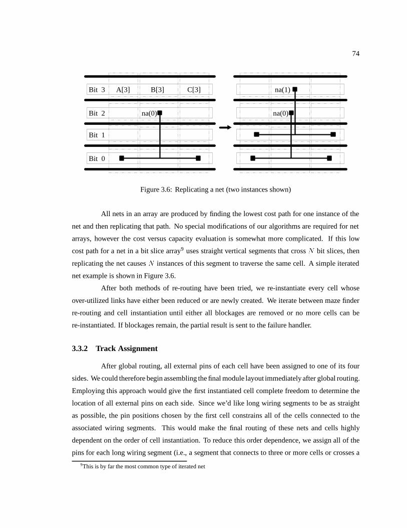
74
Bit 0
Bit 1
Bit 2
Bit 3 A[3] B[3] C[3]
na(0) na(0)
na(1)
Figure 3.6: Replicating a net (two instances shown)
All nets in an array are produced by finding the lowest cost path for one instance of the
net and then replicating that path. No special modifications of our algorithms are required for net
arrays, however the cost versus capacity evaluation is somewhat more complicated. If this low
cost path for a net in a bit slice array9 uses straight vertical segments that cross N bit slices, then
replicating the net causes N instances of this segment to traverse the same cell. A simple iterated
net example is shown in Figure 3.6.
After both methods of re-routing have been tried, we re-instantiate every cell whose
over-utilized links have either been reduced or are newly created. We iterate between maze finder
re-routing and cell instantiation until either all blockages are removed or no more cells can be
re-instantiated. If blockages remain, the partial result is sent to the failure handler.
3.3.2 Track Assignment
After global routing, all external pins of each cell have been assigned to one of its four
sides. We could therefore begin assembling the final module layout immediately after global routing.
Employing this approach would give the first instantiated cell complete freedom to determine the
location of all external pins on each side. Since we’d like long wiring segments to be as straight
as possible, the pin positions chosen by the first cell constrains all of the cells connected to the
associated wiring segments. This would make the final routing of these nets and cells highly
dependent on the order of cell instantiation. To reduce this order dependence, we assign all of the
pins for each long wiring segment (i.e., a segment that connects to three or more cells or crosses a
9This is by far the most common type of iterated net

75
cell without connecting) at once.
Besides keeping each wiring segment straight, we also want to optimize the position of
each segment relative to the others that pass through the cell. In our formulation of this assignment
problem, we consider each wiring direction separately and we further partition each sub-problem
into routing regions. For wires in the horizontal direction, each transistor row is a separate region.
The regions for vertical wires are formed by extending the vertical boundary between cells into cut-
lines that traverse the module. Within each region, the wiring assignment thus becomes analogous
to the channel routing problem[29] in general layout systems.
The primary difference between the standard channel routing formulation and our model
is that at this stage the positions of internal cell connections are as yet unknown. Our channel
model therefore abstracts each cell into two “columns” that represent the two boundaries of each
cell through which the channel’s wiring passes. Our columns differ from the standard definition
in that they may contain several connections. Nets that terminate in the cell are represented by
pseudo-pins placed at the top and bottom of the “nearest” column. Pseudo-pin pairs are placed in
both columns if a net connects to a cell and passes through it.
All horizontal channels (rows) are processed before vertical ones, and the discussion below
assumes we are working with horizontal wiring segments. Despite this, most of the items discussed
below apply directly to the track assignment for vertical wiring. Exceptions and modifications are
discussed as they arise.
We begin by making an assignment of wiring segments to channels; this is derived from the
global routing graph. To begin, we determine for each link the ordinal of the channel(s) traversed
by its corresponding boundary. A straight segment must be assigned to a channel traversed by
the boundary of every link; this is simply the intersection of the corresponding row sets. Each
segment is assignable to at least one channel, otherwise during global routing the segment would
have been split and the internal wiring load of the cell where the split occurred would have been
incremented10. Segments may be assigned to more than one channel, in which case the channel
numbers are interpreted as mutually exclusive alternatives. Segments that are instances of the same
net array are processed separately to ensure that no two instances are assigned to the same channel.
A sample segment assignment is illustrated in Figure 3.7.
Segments are assigned to tracks one channel at a time using the left-edge algorithm[23].
We use this algorithm in part because it never breaks a wiring segment, even when the segment
10Our implementation of the internal wiring load computation shares methods and results.
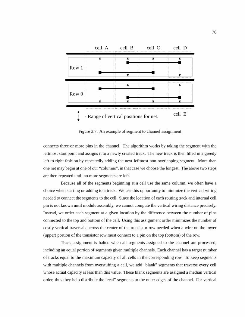
76
Row 0
Row 1
- Range of vertical positions for net.
cell A cell B cell C cell D
cell E
Figure 3.7: An example of segment to channel assignment
connects three or more pins in the channel. The algorithm works by taking the segment with the
leftmost start point and assigns it to a newly created track. The new track is then filled in a greedy
left to right fashion by repeatedly adding the next leftmost non-overlapping segment. More than
one net may begin at one of our “columns”, in that case we choose the longest. The above two steps
are then repeated until no more segments are left.
Because all of the segments beginning at a cell use the same column, we often have a
choice when starting or adding to a track. We use this opportunity to minimize the vertical wiring
needed to connect the segments to the cell. Since the location of each routing track and internal cell
pin is not known until module assembly, we cannot compute the vertical wiring distance precisely.
Instead, we order each segment at a given location by the difference between the number of pins
connected to the top and bottom of the cell. Using this assignment order minimizes the number of
costly vertical traversals across the center of the transistor row needed when a wire on the lower
(upper) portion of the transistor row must connect to a pin on the top (bottom) of the row.
Track assignment is halted when all segments assigned to the channel are processed,
including an equal portion of segments given multiple channels. Each channel has a target number
of tracks equal to the maximum capacity of all cells in the corresponding row. To keep segments
with multiple channels from overstuffing a cell, we add “blank” segments that traverse every cell
whose actual capacity is less than this value. These blank segments are assigned a median vertical
order, thus they help distribute the “real” segments to the outer edges of the channel. For vertical
77
wiring, the calculation of the number of blank segments is adjusted to take into account the variable
width of these channels. Furthermore, not all vertical blank segments are placed in the middle of
their respective channels. Instead they are evenly distributed among the “real” segments.
Although Cai et. al.[72] use a routing model in which the exact positions for pins
are known in advance, his formulation of the track assignment problem is similar. There, track
assignment is solved by recursively bi-partitioning each channel until each partition contains one
track and hence one segment. The partitioning uses terminal propagation to keep segments on
opposite sides of a cut-line close together. The Pathway datapath layout assembler[82] uses the
same track assignment formulation but uses a dynamic programming algorithm to solve it. Because
the algorithm considers all possible assignments of segments to tracks independently in each cell,
it has a worst-case complexity of O(N !) where N is the number of tracks. Several heuristics are
needed to make the execution time tractable. The LASSIE[74] system uses an industrial single layer
router in its over-the-cell model. Nakao et. al.[79] use over-the-cell routing but doesn’t specify how
it is accomplished.
Lastly, each segment is mapped to interval constraints for the external pins of each cell
traversed. We have found that interval constraints do the best job of preserving preferred wiring
locations and order while giving the cell generator the flexibility to determine the exact wiring paths
based on the internal wiring of that cell. Vertical segments are given wider intervals than horizontal
ones, in part because there is usually more space for such intervals. Also, for vertical segments
the amount of wiring needed to connect to the cell’s internals exhibits a greater dependence on the
cell’s transistor placement.
3.3.3 Module Assembly
The final layout of the module is synthesized one cell at a time by the cell generator.
The job of the module assembly stage is to choose the order of cell generation and to propagate
external pin constraints from synthesized cells to those not yet synthesized. Although the influence
of cell synthesis order has been reduced by the track assignment stage, it remains the most important
consideration at this time.
Our objective in choosing the first cell to be synthesized is to find the cell that has the
most constrained wiring problem. This allows said cell maximal freedom to find feasible routing
paths without having a portion of its external pins in fixed positions. Our preferred candidate for
initial synthesis is a cell that has been instantiated in the capacity reduction step in global routing.
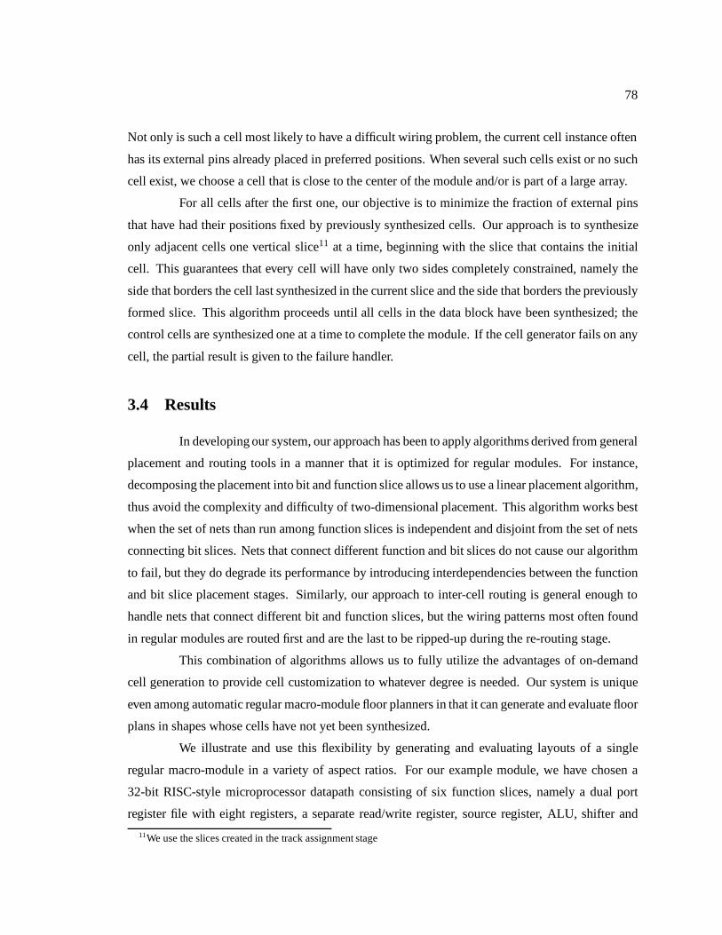
78
Not only is such a cell most likely to have a difficult wiring problem, the current cell instance often
has its external pins already placed in preferred positions. When several such cells exist or no such
cell exist, we choose a cell that is close to the center of the module and/or is part of a large array.
For all cells after the first one, our objective is to minimize the fraction of external pins
that have had their positions fixed by previously synthesized cells. Our approach is to synthesize
only adjacent cells one vertical slice11 at a time, beginning with the slice that contains the initial
cell. This guarantees that every cell will have only two sides completely constrained, namely the
side that borders the cell last synthesized in the current slice and the side that borders the previously
formed slice. This algorithm proceeds until all cells in the data block have been synthesized; the
control cells are synthesized one at a time to complete the module. If the cell generator fails on any
cell, the partial result is given to the failure handler.
3.4 Results
In developing our system, our approach has been to apply algorithms derived from general
placement and routing tools in a manner that it is optimized for regular modules. For instance,
decomposing the placement into bit and function slice allows us to use a linear placement algorithm,
thus avoid the complexity and difficulty of two-dimensional placement. This algorithm works best
when the set of nets than run among function slices is independent and disjoint from the set of nets
connecting bit slices. Nets that connect different function and bit slices do not cause our algorithm
to fail, but they do degrade its performance by introducing interdependencies between the function
and bit slice placement stages. Similarly, our approach to inter-cell routing is general enough to
handle nets that connect different bit and function slices, but the wiring patterns most often found
in regular modules are routed first and are the last to be ripped-up during the re-routing stage.
This combination of algorithms allows us to fully utilize the advantages of on-demand
cell generation to provide cell customization to whatever degree is needed. Our system is unique
even among automatic regular macro-module floor planners in that it can generate and evaluate floor
plans in shapes whose cells have not yet been synthesized.
We illustrate and use this flexibility by generating and evaluating layouts of a single
regular macro-module in a variety of aspect ratios. For our example module, we have chosen a
32-bit RISC-style microprocessor datapath consisting of six function slices, namely a dual port
register file with eight registers, a separate read/write register, source register, ALU, shifter and
11We use the slices created in the track assignment stage

79
multiplexor. Each of these cells uses a net-list that processes one bit per cell, except for the shifter,
whose smallest net-list unit processes four bits. The register file contains separate decoder cells for
each port, while all other data function blocks except the shifter have a single control cell associated
with them.
In addition to comparing the area and net-length of differently shaped floor plans at the
macro-module level, we also determine the template height requirements of individual cells in order
to augment the data presented in Chapter 2. To do this, we measure and report for each cell the
template height needed to ensure that said cell can be routed in the “loose” and “dense” forms of the
gate isolation template. By adding this value to the number of wires passing through each cell in
the chosen floor plan, we find the number of tracks needed to implement the module without adding
extra rows for wiring space.
The module layout process begins with an assessment of what module shapes are feasible;
this in turn is based on the set of feasible shapes for each cell. We have found three feasible shapes
for our example module. Expressed in terms of data cell heights, the feasible shapes are one row per
bit, two rows per bit, and three rows for two bits. The latter shape is created by merging the net-list
for all one-bit cells. Table 3.1 shows the width of each data cell for all three shapes. Summing
the data cell widths yields the width of the entire data block; this forms the last entry in Table 3.1.
There are eight registers in the register file, this is taken into account when computing the data block
width.
Looking at width alone favors denser templates and higher aspect ratios exclusively.
However, many cells are wider than might be expected, i.e. a dense cell at a given shape is not
always half the width of its loose counterpart, and a cell with a height of two rows per bit may
be more than half the width of a cell with a height of one row per bit. Some of the increase
occurs because the layouts for higher aspect ratios have lower site utilization. However, we have
found that increases in width is often due to the need to add routing space to accommodate vertical
congestion. Higher aspect ratio layouts contain a large amount of inter-row wiring; this effect is
most pronounced in large cells (e.g. the ALU and shifter). In small cells, the additional routing
space is needed to accommodate vertical control signals passing through the cell. This effect is
most pronounced in the dense template versions of the two port register file cell and the multiplexor
cell. These cells must accommodate four and six vertical control signals respectively.
Ideally, the widths of the control cell for a function slice would be less than the width
of its corresponding data cell, this guarantees that a control cell will not increase the width of the
module. Thus, we use the widths found in Table 3.1 as a target for control cell synthesis. The
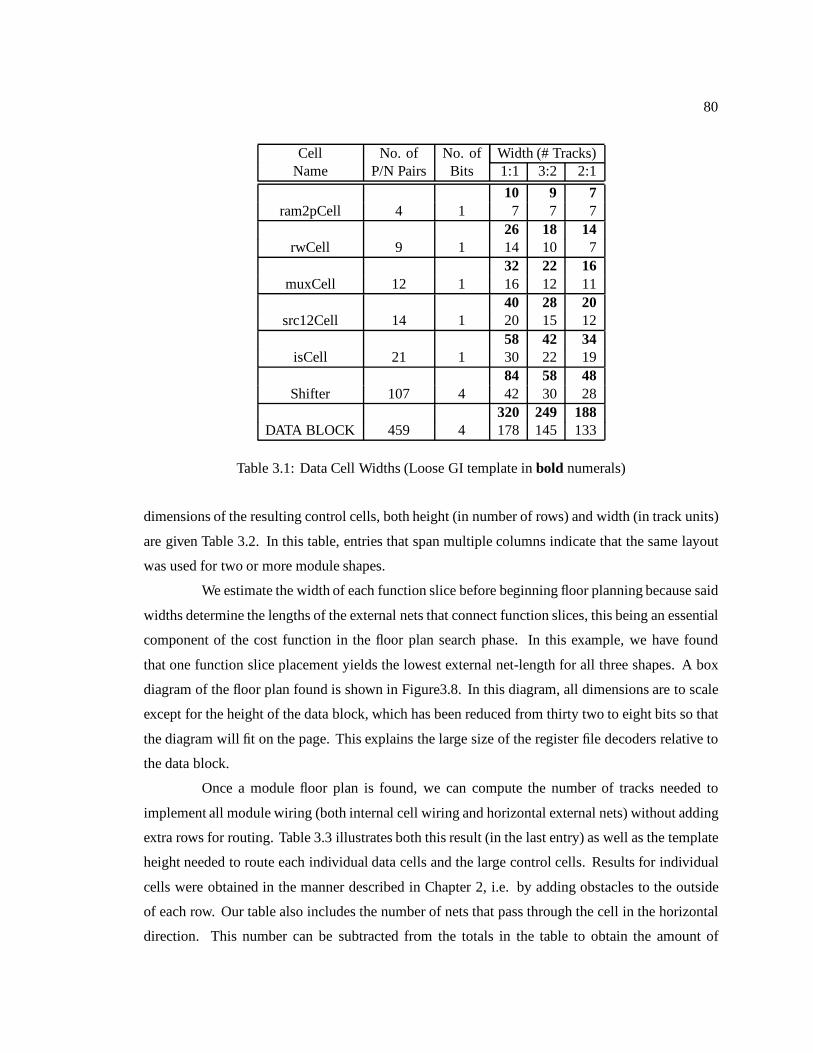
80
Cell No. of No. of Width (# Tracks)Name P/N Pairs Bits 1:1 3:2 2:1
10 9 7ram2pCell 4 1 7 7 7
26 18 14rwCell 9 1 14 10 7
32 22 16muxCell 12 1 16 12 11
40 28 20src12Cell 14 1 20 15 12
58 42 34isCell 21 1 30 22 19
84 58 48Shifter 107 4 42 30 28
320 249 188DATA BLOCK 459 4 178 145 133
Table 3.1: Data Cell Widths (Loose GI template in bold numerals)
dimensions of the resulting control cells, both height (in number of rows) and width (in track units)
are given Table 3.2. In this table, entries that span multiple columns indicate that the same layout
was used for two or more module shapes.
We estimate the width of each function slice before beginning floor planning because said
widths determine the lengths of the external nets that connect function slices, this being an essential
component of the cost function in the floor plan search phase. In this example, we have found
that one function slice placement yields the lowest external net-length for all three shapes. A box
diagram of the floor plan found is shown in Figure3.8. In this diagram, all dimensions are to scale
except for the height of the data block, which has been reduced from thirty two to eight bits so that
the diagram will fit on the page. This explains the large size of the register file decoders relative to
the data block.
Once a module floor plan is found, we can compute the number of tracks needed to
implement all module wiring (both internal cell wiring and horizontal external nets) without adding
extra rows for routing. Table 3.3 illustrates both this result (in the last entry) as well as the template
height needed to route each individual data cells and the large control cells. Results for individual
cells were obtained in the manner described in Chapter 2, i.e. by adding obstacles to the outside
of each row. Our table also includes the number of nets that pass through the cell in the horizontal
direction. This number can be subtracted from the totals in the table to obtain the amount of
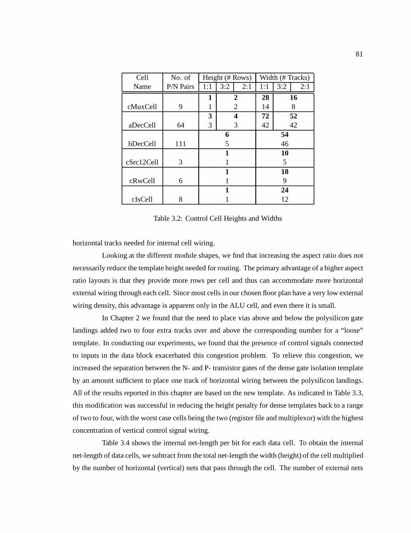
81
Cell No. of Height (# Rows) Width (# Tracks)Name P/N Pairs 1:1 3:2 2:1 1:1 3:2 2:1
1 2 28 16cMuxCell 9 1 2 14 8
3 4 72 52aDecCell 64 3 3 42 42
6 54bDecCell 111 5 46
1 10cSrc12Cell 3 1 5
1 18cRwCell 6 1 9
1 24cIsCell 8 1 12
Table 3.2: Control Cell Heights and Widths
horizontal tracks needed for internal cell wiring.
Looking at the different module shapes, we find that increasing the aspect ratio does not
necessarily reduce the template height needed for routing. The primary advantage of a higher aspect
ratio layouts is that they provide more rows per cell and thus can accommodate more horizontal
external wiring through each cell. Since most cells in our chosen floor plan have a very low external
wiring density, this advantage is apparent only in the ALU cell, and even there it is small.
In Chapter 2 we found that the need to place vias above and below the polysilicon gate
landings added two to four extra tracks over and above the corresponding number for a “loose”
template. In conducting our experiments, we found that the presence of control signals connected
to inputs in the data block exacerbated this congestion problem. To relieve this congestion, we
increased the separation between the N- and P- transistor gates of the dense gate isolation template
by an amount sufficient to place one track of horizontal wiring between the polysilicon landings.
All of the results reported in this chapter are based on the new template. As indicated in Table 3.3,
this modification was successful in reducing the height penalty for dense templates back to a range
of two to four, with the worst case cells being the two (register file and multiplexor) with the highest
concentration of vertical control signal wiring.
Table 3.4 shows the internal net-length per bit for each data cell. To obtain the internal
net-length of data cells, we subtract from the total net-length the width (height) of the cell multiplied
by the number of horizontal (vertical) nets that pass through the cell. The number of external nets
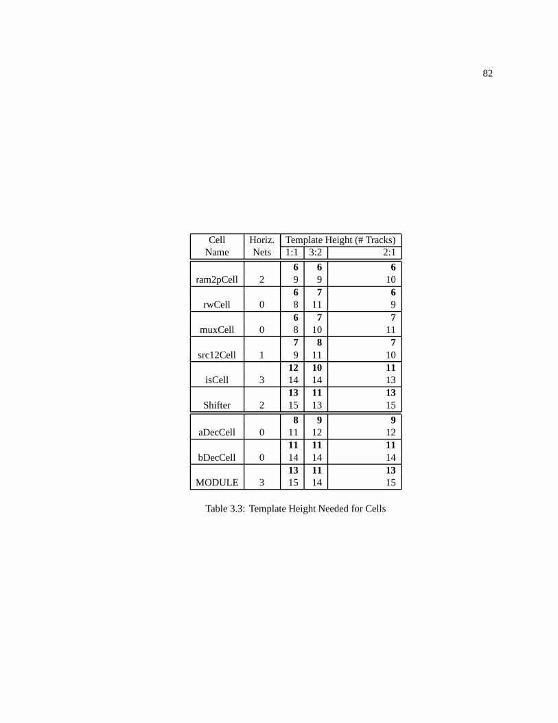
82
Cell Horiz. Template Height (# Tracks)Name Nets 1:1 3:2 2:1
6 6 6ram2pCell 2 9 9 10
6 7 6rwCell 0 8 11 9
6 7 7muxCell 0 8 10 11
7 8 7src12Cell 1 9 11 10
12 10 11isCell 3 14 14 13
13 11 13Shifter 2 15 13 15
8 9 9aDecCell 0 11 12 12
11 11 11bDecCell 0 14 14 14
13 11 13MODULE 3 15 14 15
Table 3.3: Template Height Needed for Cells
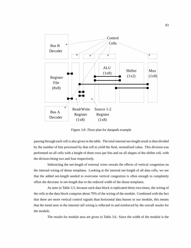
83
Register File (8x8)
Bus ADecoder
Bus BDecoder
Shifter (1x2)
Mux(1x8)
ALU(1x8)
Read/Write Register (1x8)
Source 1-2 Register (1x8)
Control Cells
Figure 3.8: Floor plan for datapath example
passing through each cell is also given in the table. The total internal net-length result is then divided
by the number of bits processed by that cell to yield the final, normalized value. This division was
performed on all cells with a height of three rows per bits and on all shapes of the shifter cell, with
the divisors being two and four respectively.
Subtracting the net-length of external wires reveals the effects of vertical congestion on
the internal wiring of dense templates. Looking at the internal net-length of all data cells, we see
that the added net-length needed to overcome vertical congestion is often enough to completely
offset the decrease in net-length due to the reduced width of the dense templates.
As seen in Table 3.5, because each data block is replicated thirty-two times, the wiring of
the cells in the data block comprise about 70% of the wiring of the module. Combined with the fact
that there are more vertical control signals than horizontal data busses in our module, this means
that the trend seen in the internal cell wiring is reflected in and reinforced by the overall results for
the module.
The results for module area are given in Table 3.6. Since the width of the module is the
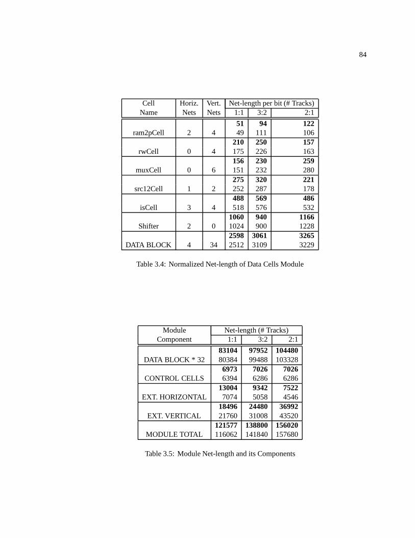
84
Cell Horiz. Vert. Net-length per bit (# Tracks)Name Nets Nets 1:1 3:2 2:1
51 94 122ram2pCell 2 4 49 111 106
210 250 157rwCell 0 4 175 226 163
156 230 259muxCell 0 6 151 232 280
275 320 221src12Cell 1 2 252 287 178
488 569 486isCell 3 4 518 576 532
1060 940 1166Shifter 2 0 1024 900 1228
2598 3061 3265DATA BLOCK 4 34 2512 3109 3229
Table 3.4: Normalized Net-length of Data Cells Module
Module Net-length (# Tracks)Component 1:1 3:2 2:1
83104 97952 104480DATA BLOCK * 32 80384 99488 103328
6973 7026 7026CONTROL CELLS 6394 6286 6286
13004 9342 7522EXT. HORIZONTAL 7074 5058 4546
18496 24480 36992EXT. VERTICAL 21760 31008 43520
121577 138800 156020MODULE TOTAL 116062 141840 157680
Table 3.5: Module Net-length and its Components
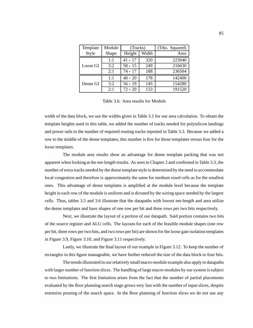
85
Template Module (Tracks) (Trks. Squared)Style Shape Height Width Area
1:1 41 � 17 320 223040Loose GI 3:2 58 � 15 249 216630
2:1 74 � 17 188 236504
1:1 40 � 20 178 142400Dense GI 3:2 56 � 19 145 154280
2:1 72 � 20 133 191520
Table 3.6: Area results for Module
width of the data block, we use the widths given in Table 3.1 for our area calculation. To obtain the
template heights used in this table, we added the number of tracks needed for polysilicon landings
and power rails to the number of required routing tracks reported in Table 3.3. Because we added a
row to the middle of the dense templates, this number is five for those templates versus four for the
loose templates.
The module area results show an advantage for dense template packing that was not
apparent when looking at the net-length results. As seen in Chapter 2 and confirmed in Table 3.3, the
number of extra tracks needed by the dense template style is determined by the need to accommodate
local congestion and therefore is approximately the same for medium sized cells as for the smallest
ones. This advantage of dense templates is amplified at the module level because the template
height in each row of the module is uniform and is dictated by the wiring space needed by the largest
cells. Thus, tables 3.5 and 3.6 illustrate that the datapaths with lowest net-length and area utilize
the dense templates and have shapes of one row per bit and three rows per two bits respectively.
Next, we illustrate the layout of a portion of our datapath. Said portion contains two bits
of the source register and ALU cells. The layouts for each of the feasible module shapes (one row
per bit, three rows per two bits, and two rows per bit) are shown for the loose gate isolation templates
in Figure 3.9, Figure 3.10, and Figure 3.11 respectively.
Lastly, we illustrate the final layout of our example in Figure 3.12. To keep the number of
rectangles in this figure manageable, we have further reduced the size of the data block to four bits.
The trends illustrated in our relatively small macro-module example also apply to datapaths
with larger number of function slices. The handling of large macro-modules by our system is subject
to two limitations. The first limitation arises from the fact that the number of partial placements
evaluated by the floor planning search stage grows very fast with the number of input slices, despite
extensive pruning of the search space. In the floor planning of function slices we do not use any

86
heuristics that could exclude the placement with absolute minimum cost. Thus, this complexity
places a limit on the the number of function slices that may be searched in a reasonable amount of
CPU time.
The performance of the search algorithm, measured by the exact number of slices that
may be handled, is difficult to quantify in a manner that produces results that may be compared with
other tools. We found that the number of evaluated partial solutions generated and evaluated is a
strong function of both the number nets and the number of pins per net. A net with a large number of
pins connects many blocks together; this in turn leads to the generation of many partial placements
solutions with approximately the same cost. By contrast, if the same blocks are connected by a
number of two pin nets, fewer solutions will have a cost near to the optimal one (i.e. placing the
connected blocks side by side). The algorithm can handle many blocks connected in this fashion.
We have found that two examples with the same number of blocks and pins may produce run times
that differ widely (i.e. by a factor of five). Unfortunately, the connectivity details of datapath
examples presented in other publications are unavailable. Thus, the only comparative result we
have is that our algorithm is neither significantly faster nor significantly slower than other published
ones.
To determine the limit of our floor plan search stage in the worst case, we created a family
of related datapaths by introducing multiple instances of the six function slices in our original
example connected by nets with a large number of pins (i.e. slightly fewer than the total number
of blocks). We found that our floor planner can handle up to 15 function slices connected in this
manner using less than one hour of CPU time on a Sun SparcStation One without the need for
partitioning or other complexity reducing measures. Reducing the connectivity to a median value
(i.e. each nets connects half the slices in the module) increases the number of blocks processed
in one CPU hour to 19. This implies that all but the largest datapaths may be searched without
heuristics, thereby retaining the guarantee that the lowest cost overall solution will be found.
The amount of time spent on the function slice placement dominates the entire layout
process, including bit slice placement. Even though bit slices are placed with the same basic
algorithm used in function slice placement, nets in bit slices connect to either all slices or only two
slices. The run time may thus be made negligible by eliminating the nets that connect to all blocks
and by generating no partial solution with two adjacent disconnected slices.
Another problem with handling large datapaths in our system is that the number of data
busses passing through the cells increases with the number of function slices. Thus, routing all
wires inside transistor rows may not be practical for large datapaths. The result tables above show

87
that at least one proposed remedy to this problem, namely using module layouts with more rows
per bit, is of limited usefulness due to the increases in vertical and internal wiring length. Other
potential remedies, explored in Chapter 4, include adding rows for routing space and changing floor
plan placements to reduce the wiring density while possibly increasing net-length.
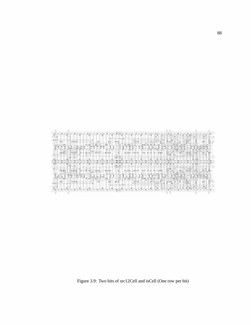
88
Figure 3.9: Two bits of src12Cell and isCell (One row per bit)
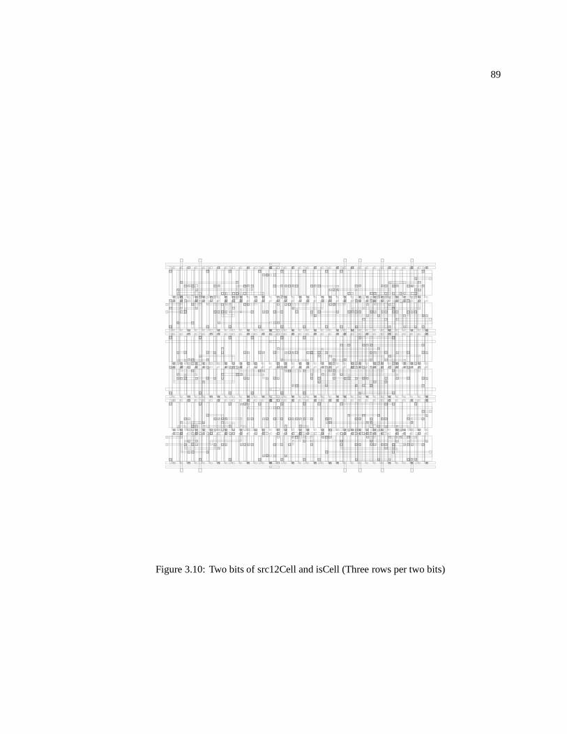
89
Figure 3.10: Two bits of src12Cell and isCell (Three rows per two bits)
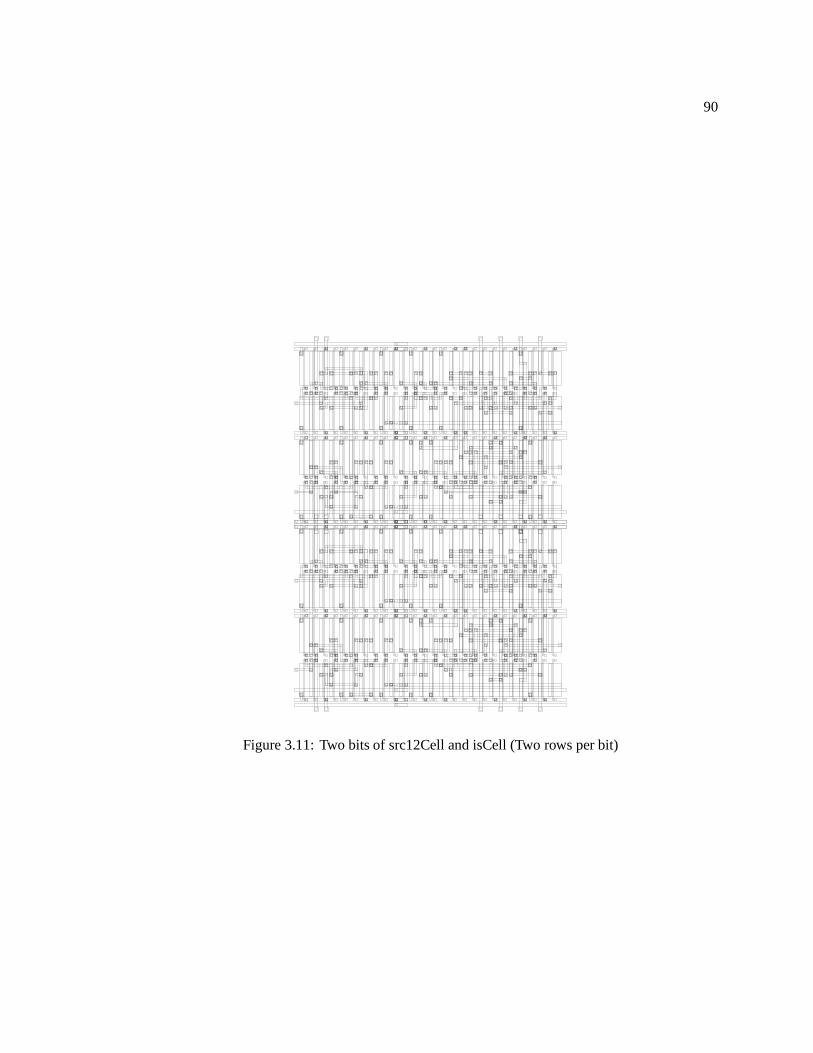
90
Figure 3.11: Two bits of src12Cell and isCell (Two rows per bit)
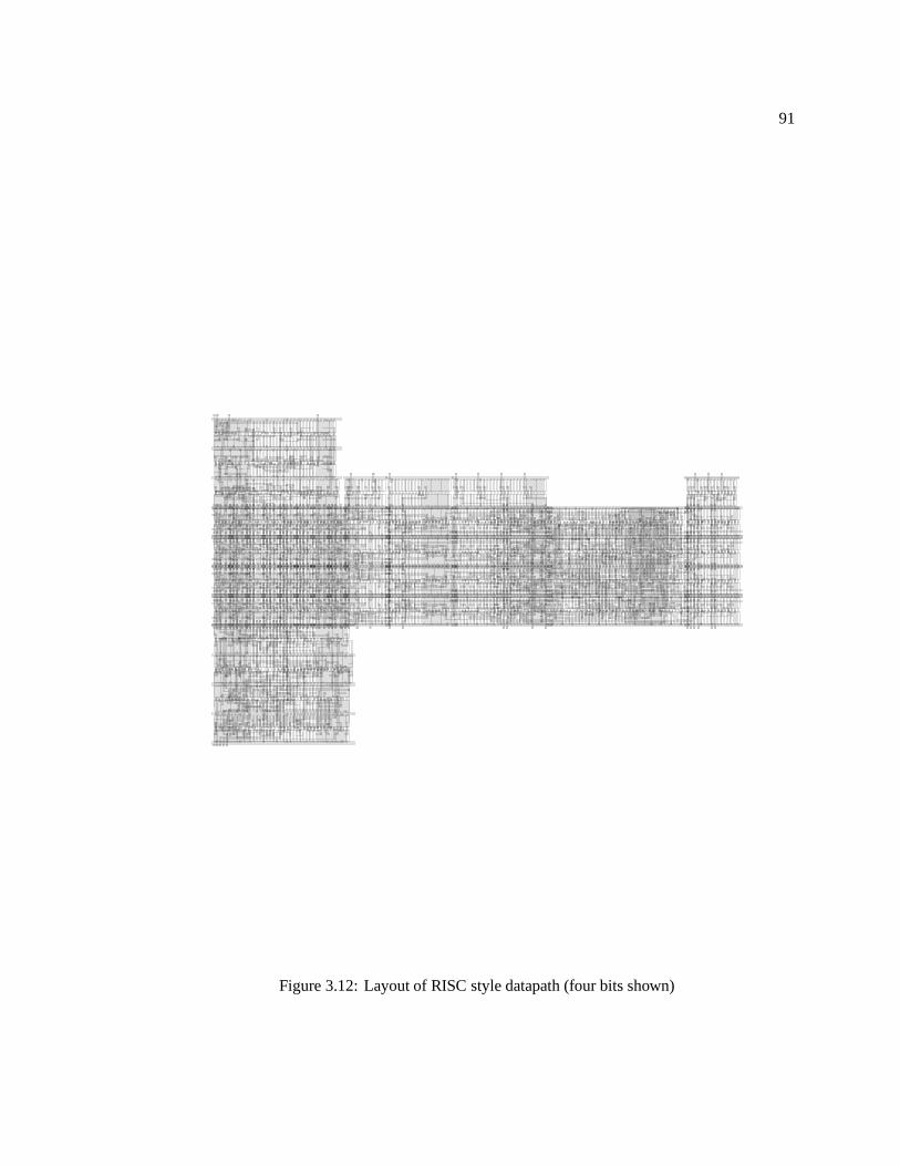
91
Figure 3.12: Layout of RISC style datapath (four bits shown)
92
Chapter 4
The Elements of Non-Sequential Tool
Interaction
Any layout system may be viewed as containing the following elements:
� A set of tools that collectively can perform the entire layout task.
� A method of communicating information about the state of the design among these tools.
� A strategy for controlling the pattern of tool invocations that results in a particular design
path.
This chapter focuses on the latter two elements because they implement the model that
governs tool interaction in the system. Hence, the properties of tool interaction defined in Chapter
1 may be expressed as requirements imposed on these elements. Recall that in non-sequential
tool interaction the intermediate results produced by each tool help determine subsequent tool
invocations. Any implementation of non-sequential tool interaction must therefore possess an
element that uses the current design state to select a tool invocation from two or more choices.
Similarly, supporting two-way interaction among N tools requires a communication method that
supplies either a view of the design state that is shared among all tools or N(N � 1) customized
links between pairs of tools.
Formulating these requirements allows us to compare and contrast diverse implementa-
tions of non-sequential and/or two-way tool interaction, including those implementations whose
elements are defined implicitly. For instance, the methods of integrating placement and routing
described in Chapter 1 may be viewed as examples of two-way interaction with the single common
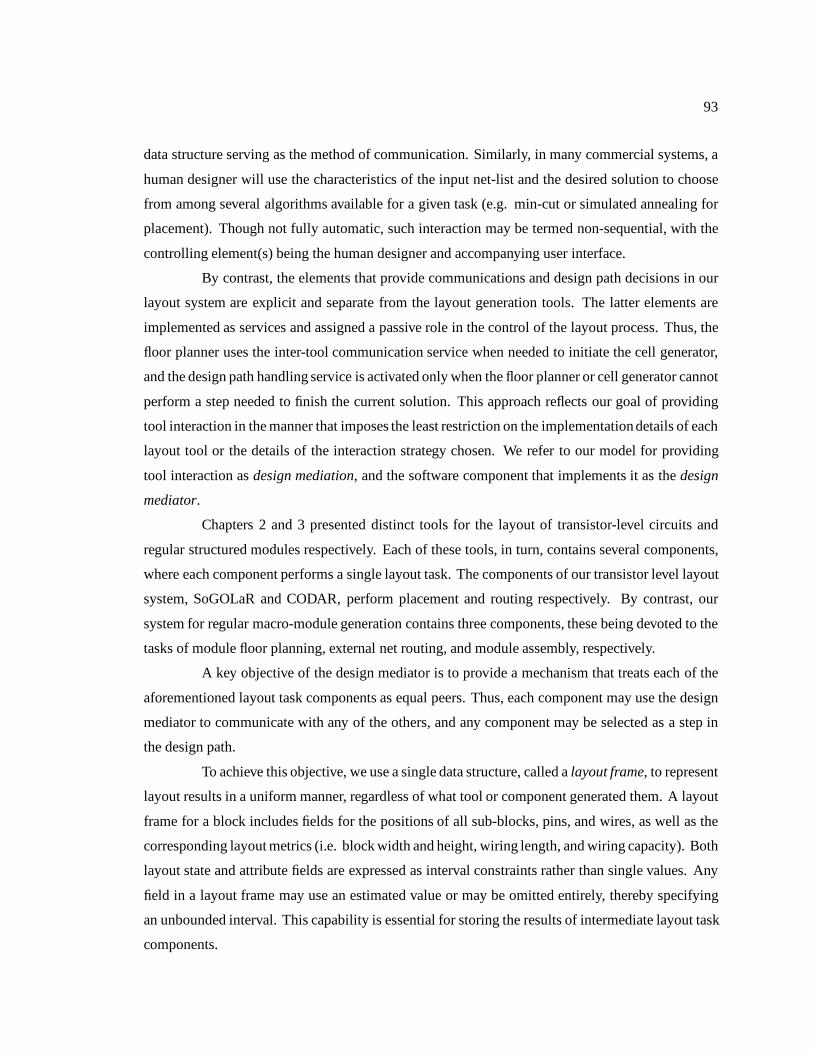
93
data structure serving as the method of communication. Similarly, in many commercial systems, a
human designer will use the characteristics of the input net-list and the desired solution to choose
from among several algorithms available for a given task (e.g. min-cut or simulated annealing for
placement). Though not fully automatic, such interaction may be termed non-sequential, with the
controlling element(s) being the human designer and accompanying user interface.
By contrast, the elements that provide communications and design path decisions in our
layout system are explicit and separate from the layout generation tools. The latter elements are
implemented as services and assigned a passive role in the control of the layout process. Thus, the
floor planner uses the inter-tool communication service when needed to initiate the cell generator,
and the design path handling service is activated only when the floor planner or cell generator cannot
perform a step needed to finish the current solution. This approach reflects our goal of providing
tool interaction in the manner that imposes the least restriction on the implementation details of each
layout tool or the details of the interaction strategy chosen. We refer to our model for providing
tool interaction as design mediation, and the software component that implements it as the design
mediator.
Chapters 2 and 3 presented distinct tools for the layout of transistor-level circuits and
regular structured modules respectively. Each of these tools, in turn, contains several components,
where each component performs a single layout task. The components of our transistor level layout
system, SoGOLaR and CODAR, perform placement and routing respectively. By contrast, our
system for regular macro-module generation contains three components, these being devoted to the
tasks of module floor planning, external net routing, and module assembly, respectively.
A key objective of the design mediator is to provide a mechanism that treats each of the
aforementioned layout task components as equal peers. Thus, each component may use the design
mediator to communicate with any of the others, and any component may be selected as a step in
the design path.
To achieve this objective, we use a single data structure, called a layout frame, to represent
layout results in a uniform manner, regardless of what tool or component generated them. A layout
frame for a block includes fields for the positions of all sub-blocks, pins, and wires, as well as the
corresponding layout metrics (i.e. block width and height, wiring length, and wiring capacity). Both
layout state and attribute fields are expressed as interval constraints rather than single values. Any
field in a layout frame may use an estimated value or may be omitted entirely, thereby specifying
an unbounded interval. This capability is essential for storing the results of intermediate layout task
components.
94
Name:
Metric:
Value:
Weight:
Buscap Width Height
Pin Constraints Layout State
lowerupper
Figure 4.1: Example of a layout frame.
The layout frame, in turn, forms the basis of that portion of the design mediator devoted
to providing inter-tool communication. The core of this service consists of a database of attempted
layout implementations for the entire module and for each cell in it. The database is accessed by
placing the desired constraints and layout metrics into a layout frame known as the request frame.
When a request is received, the server will first try to match the constraints in the request frame with
the results of a previously handled request. If a match is found, the server simply returns the results
of the attempted implementation, whether successful or unsuccessful. If a layout with the particular
set of attributes requested has not been attempted before, the server dispatches the appropriate tool
and task component to attempt an implementation with the given constraints and then records as
well as returns that result.
The attributes used in frame comparison, namely net-length, density, and area, are metrics
that are meaningful to both the floor planner and cell generator. This allows all frame requests to be
handled in a uniform manner, regardless of what tool originated the request. Storing both successful
and unsuccessful attempts enables the layout tools to communicate not only what layouts have been
already produced but also what metrics do (or do not) result in feasible layout. Collectively, these
properties allow the tools in our system to share information about the emerging layout solution
while imposing minimal restrictions on when or how said sharing should take place. Figure 4.1
illustrates a layout frame.
This latter point is best illustrated through the different ways in which our system uses
the layout database and layout frames. As described throughout Chapter 3, the floor planner uses
the layout database both to establish the range of metrics feasible for a cell and to request a specific
95
implementation for use in module assembly. The cell generator may in turn pre-load cells into the
database. This is used either to indicate preferred implementations or to define those layout metrics
that are known to be infeasible. Finally, the design mediator itself uses layout frames both to store
the intermediate results of the layout process and to capture the designer’s constraint specifications
at the start of the process.
Besides the aforementioned tasks, the layout database also plays an essential role in our
strategy for implementing non-sequential design path control. This failure handler portion of the
design mediator is invoked only when the currently chosen floor plan cannot be routed or no longer
meets a specified constraint. Stated briefly, the failure handler’s objective is to restart the layout
process on a design path that will lead to a successful conclusion. To do this, it must first modify
the current design state to avoid a repetition of the actions that resulted in the current unsatisfactory
state and (whenever possible) guide the synthesis tools toward a more promising solution. For these
purposes, the design state consists of the input net-list and the set of constraints that describe the
current layout metrics as well as the current block and pin positions. Except for the input net-list,
which is shared among all the layout tools, all this information is provided to the failure handler by
the synthesis tools using the communications method described above.
We have chosen to formulate the task in terms of transforming the design state, as opposed
to the specifics of the layout process, so that the failure handler can operate independently of the
implementation details of the layout tools. In our formulation, the current design state is simply
a set of constraints that cannot be met. The failure handler focuses on the direct manipulation of
these constraints. Our ability to perform these manipulations is greatly enhanced by our use of a
single layout frame structure to represent said constraints.
The number of layout state constraints (and possible changes thereto) is quite large,
and we have found that actions to correct constraint violations are useful only in a narrow set of
circumstances. Thus, we begin failure handling by attempting to classify the failures present in the
current design state. We group all failures that halt the synthesis process prematurely (e.g. a cell
won’t route) into a single category, while completed layouts that fail to meet one or more constraints
are placed into separate categories based on what constraint(s) were violated. These categories
include the overall width, height, and net-length for the module, as well as the length of each net.
We refer to any change to the current design state by the failure handler as an action.
Formulated in these terms, the objective of the failure handler is to find a set of actions capable
of removing all constraint violations in the current design state; we call such a set a remedy. The
handler first attempts to apply remedies that remove constraints in a straightforward manner. These
96
direct remedies are self-contained attempts to produce a failure free design state from the current
one; intuitively, they correspond to applying a “patch” to fix the problem. Direct remedies may
include, for instance, re-routing a single external net or re-synthesizing a cell after slightly altering
its external pin constraints.
Although any type of constraint manipulation can form part of a direct remedy, to be
included in this stage there must be an easy method of determining whether the remedy in fact
removes the constraint violation. A successful direct remedy must also produce a design state
from which the synthesis process can resume where it left off. These restrictions mean that for
some failures, no direct remedy will be found. Even when a potentially successful remedy is
found, applying said remedy may produce a constraint violation of a more difficult to handle type.
Furthermore, not all remedies may be combined; this implies that a set of constraint violations may
have no direct remedy, even when each violation considered individually has a remedy.
Because of the aforementioned problems, direct remedies are insufficient to remove all
possible constraint violations, and design states exist for which no direct remedy is applicable.
Thus, the failure handler also uses remedies that discard a portion of the current design state. We
call these remedies indirect because the failure handler undoes previous work to produce a design
state that is a suitable starting point for re-synthesis, rather than attempting to produce an alternative
solution by itself.
In the design of remedies, we assume that, on each invocation, each tool performs as well
as possible given the set of constraints at its input. Thus, in order for a remedy to reduce a particular
layout metric, there must exist another metric for which a tradeoff is applicable. That is, we never
simply resend the same request to the layout database in the hope of obtaining a better result.
During the course of its application, each remedy may introduce new types of constraint
violations. This implies that the set of potentially useful remedies changes unpredictably as each
remedy is applied. Because we cannot easily undo the application of a remedy, executing even a
simple control sequence (e.g. execute remedy B if remedy A doesn’t correct the failure) requires
that we keep “before” and “after” copies of the entire design state. Thus, implementing a standard
backtracking algorithm for controlling the application of remedies would require exceedingly large
amounts of storage.
To solve these problems, we rely on the layout database to avoid repeating unproductive
remedies. Because failed as well as successful requests are stored there, we can determine whether
a remedy has been applied before by querying the layout database using the design state at the point
where the synthesis process would be restarted. Often, we need only use a subset of the design state
97
(usually the part that is altered by the candidate remedy) for the query. By altering the constraints
in the query, we can attain a finer degree of control over remedy acceptance criteria compared to
explicitly checking the design path history.
In altering the inputs to the layout process, we want not only to avoid unnecessary
repetition but to pro-actively improve our chances of finding a successful design path as well. In
part, we accomplish this by changing objective constraints given to the synthesis tools. We use this
mechanism primarily to make tradeoffs among layout metrics. For instance, if a particular cell’s
instantiation is wider than expected, the failure handler may respond by reducing the targeted widths
of other cells in the module.
We have found that changing objectives in a “top-down” fashion is not sufficient to
convey all of the information available to the failure handler. Thus, we also include a “bottom-
up” mechanism that allows the failure handler (and only the failure handler) to instruct the layout
database to exclude certain candidates from becoming the response to a query. This is implemented
via exclusion templates that specify additional constraints that must be met by the response candidate.
When specifying exclusion templates, the failure handler also specifies (via another template) the
class of templates to which it will apply. Since they work by excluding portions of the set of possible
layouts, both of the aforementioned mechanisms are applied sparingly to avoid excluding the lowest
cost solution. These mechanisms ensure that every failure will be handled by invoking an orderly
sequence of remedies that are progressively more global in scope.
The idea of supporting non-monotonic design paths and flexible inter-tool communication
has been explored in previous layout systems, most notably in Cadre[83] and the Layout Expert
System (LES)[84]. Both systems are comprised of rule-based agents where each agent performs
a layout task. In the Cadre system, communications and control are centralized in a separate
supervisor tool. By contrast, design path control in LES is distributed among the layout agents.
These agents are coupled very tightly via a shared data structure known as a “blackboard”. The
blackboard itself is simply a storage medium that uses a common format; deciding what to store
and what to communicate is entirely up to the layout agents.
As explicitly mentioned in their descriptions, both systems are sufficiently powerful and
general to implement a model of non-sequential tool interaction. However, no such model has been
described in any publication about either system. Instead, emphasis has been placed on describing
the issues that arise when developing rule-based agents for layout tasks. By contrast, our control and
communications model directly result from our desire to use known good algorithms for individual
layout tasks and the lack of an all-encompassing paradigm to bind these tools together.
98
The rest of this chapter presents the details of our communications and design path control
models. We begin the next section by describing how layout frames are constructed and used in
layout database queries. We then describe how the synthesis tools are dispatched to handle queries
whose results are not already stored in the database. In the following section, we describe in detail
our failure handling strategies and their implementation. Lastly, we illustrate how the failure handler
and layout database work using both manufactured test cases and actual layouts.
4.1 A Model for Inter-Tool Communications
4.1.1 Overview
For the purposes of modeling and implementing mechanism for tool interaction, we
consider each layout task at both module and cell level to be performed by a distinct tool. This
means that there are a total of five tools in our system, with three tools being devoted to module
level layout and two tools devoted to transistor level layout. The function of each module level tool
may be summarized as follows:
Floor Planner Assigns all cells in the module to relative positions.
Global Router Given a module floor plan, assigns wiring paths for all nets that connect two or
more cells to an unambiguous set of cell boundaries.
Module Assembler Given a floor plan and global routing, propagates the constraints necessary to
synthesize the layouts of each cell such that they may be abutted to form the layout of the
module.
Similarly, the function of each transistor level tool is summarized below:
SoGOLaR Assigns all transistors in the net-list of a cell to unique slots in a Sea-of-Gates template
array.
CODAR Given an assignment of transistors to template slots, wires all nets connecting these
transistors and assigns positions for all external pins of these nets.
Although each tool has a distinct function, they all perform this function on a single
design state, represented by a module net-list and a set of instances representing partially completed
layout results for each of the blocks, sub-blocks and cells in the net-list. Because the pattern of tool
99
invocations (i.e. the design path) is not fixed in advance, each of these tool may in fact communicate
the design state to any of the others. In particular, our use of on-demand cell generation means that
the floor planner regularly communicates cell instances to and from the cell generator, even though
some of the instances do not become part of the current design state.
These considerations compel us to develop a single comprehensive model for inter-tool
communication, rather than developing separate customized exchange mechanisms for each pair
of tools. We base our model of inter-tool communications on a common representation of layout
instance information called the layout frame. We thus begin our discussion with a sub-section
that describes the contents of the layout frame data structure and the operations associated with
it. These operations in turn form the basis for the layout database; this being a common method
of storing, accessing, and updating all layout information. All tools in our system, including the
failure handler, access the layout database by constructing a request frame with the desired layout
attributes and invoking a single query routine. The details of this query routine are discussed in the
last sub-section. That discussion does not include certain enhancements that are used exclusively
by the failure handler; these are deferred to the section on failure handling.
4.1.2 The Layout Frame
A layout frame annotates its corresponding block in the net-list with all of the information
necessary to reproduce the layout state it represents. These annotations include the positions of
blocks, pins and wires. A frame also contains fields for layout metrics, including block width and
height, wiring length for each of the nets in the block, and the wiring capacity across the block in
both the vertical and horizontal direction. All of these data are expressed as interval constraints.
Additionally, the frame also contains a weight value for each layout metric interval. Lastly,
the frame has a status field that may assume one of the following values, (SUCCESSFUL, FAILED,
PENDING), to indicate whether the frame represents a successful or failed attempt at layout or a
pending database query.
A layout frame does not contain any explicit indication of what tool(s) produced its
contents. Instead, we provide an operation that determines what tool (module or cell generator)
should be associated with a frame and what finished layout tasks are reflected in its contents. The
former is determined by the level of the net-list hierarchy (module or cell) occupied by the block
described in the frame. The degree of task completion may be found by noting that each tool
modifies the design state by adding constraints to block and/or pin positions in a distinct way.
100
The latter observation implies that we can check constraints in a layout frame to determine
whether tasks in the layout process have been finished. At the module level, the floor planner assigns
block positions and assigns the pins for nets that connect blocks to a particular side of the block.
Thus, by checking that all sub-blocks in a (module) frame are assigned fixed positions and all pins of
top-level nets are assigned to a side of their block, we may determine whether that frame completely
specifies a module floor plan. External net routing is considered finished if and only if all external
pins attached to cells are fixed to one of the four sides of that cell, and a cell is considered to have
finished module assembly if and only if those same pins occupy non-overlapping positions. A
similar, but simpler, decision tree exists for cell level frames.
The other essential operation on layout frames (besides storage and retrieval) is constraint
satisfaction checking. Since all constraints are expressed as intervals of non-negative length, a
constraintAi in frameA is characterized by the pair of values (min(Ai);max(Ai)). ConstraintAi is
said to satisfy the corresponding constraintBi in frameB if and only if interval (min(Ai);max(Ai))
lies entirely within interval (min(Bi);max(Bi)). This is true when min(Ai) >= min(Bi) and
max(Ai) <= max(Bi). We say frameA satisfies frameB if and only if every constraintAi satisfies
its corresponding constraint Bi. Objects whose position is defined by two dimensions require an
additional check to ensure that they occupy the same position in the other dimension and the same
orientation. For example, a pin position constraint on a block must either occupy the same side of
the block (if it’s a boundary pin) or the same track number and orientation (if it’s an interior pin).
4.1.3 Handling Database Queries
Both of the layout frame operations described above play an essential role in the database
query routine. Recall that any tool can initiate a query by composing a request frame that contains
the desired constraints. The query routine will first try to match the constraints in the request frame
with stored frames that represent the results of previously attempted layout implementations. This
is accomplished using frame satisfaction checking.
The query routine begins by finding all frames that represent successful layouts and satisfy
the request frame. If more than one successful candidate satisfies the request frame, we order them
by computing the weighted sum of layout metric values and return the best one. The weights used in
this calculation are supplied by the request frame. We use the most optimistic value of each layout
metric interval; for all metrics except wiring capacity this is the minimum value. We illustrate an
example of frame selection in the “successful” case in Figure 4.2. In this example, applying the
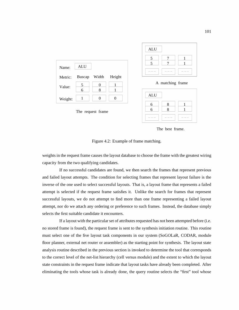
101
Name:
Metric:
Value:
Weight:
Buscap Width Height
ALU
ALU
ALU
58
11
1 0 0
55
77
11
116
6 88
06
The request frame
A matching frame
The best frame.
Figure 4.2: Example of frame matching.
weights in the request frame causes the layout database to choose the frame with the greatest wiring
capacity from the two qualifying candidates.
If no successful candidates are found, we then search the frames that represent previous
and failed layout attempts. The condition for selecting frames that represent layout failure is the
inverse of the one used to select successful layouts. That is, a layout frame that represents a failed
attempt is selected if the request frame satisfies it. Unlike the search for frames that represent
successful layouts, we do not attempt to find more than one frame representing a failed layout
attempt, nor do we attach any ordering or preference to such frames. Instead, the database simply
selects the first suitable candidate it encounters.
If a layout with the particular set of attributes requested has not been attempted before (i.e.
no stored frame is found), the request frame is sent to the synthesis initiation routine. This routine
must select one of the five layout task components in our system (SoGOLaR, CODAR, module
floor planner, external net router or assembler) as the starting point for synthesis. The layout state
analysis routine described in the previous section is invoked to determine the tool that corresponds
to the correct level of the net-list hierarchy (cell versus module) and the extent to which the layout
state constraints in the request frame indicate that layout tasks have already been completed. After
eliminating the tools whose task is already done, the query routine selects the “first” tool whose
102
synthesis task is not already done, where the ordering of tools is given by the normal, sequential
design path. Given this selection, the routine then translates the constraint information in the request
frame to a format suitable for the selected tool’s input.
The flexibility of this dispatching mechanism allows us to accommodate all access to the
synthesis tools through the request function of the layout database. Indeed, our system is initialized
by reading in user specified constraints and then creating a request frame with those inputs and
sending it to the layout database.
Once initiated, the layout synthesis process may proceed without interacting with the
design mediator. When results are returned to the query routine, the routine checks whether
the output represents a complete layout (as opposed to an intermediate result) and whether the
results satisfy the constraints specified in the request frame. Successful intermediate results are
recorded as a separate frame with a “PENDING” status. If said frame represents the top-level
block of the module, it is recorded as the current design state. Successful final results are given
the “SUCCEEDED” status, added to the database, and returned to the originator of the request.
In the absence of a pro-active failure handling strategy, any failure, whether in the final or in an
intermediate result, is recorded in the database and returned with a “FAILED” status.
Lastly, the entire dispatch mechanism may be overridden on a per request basis by the
originator of the query. If an override is applied, no results are stored in the database, and the request
frame will be returned as if the requested layout had been attempted and failed.
4.2 A Strategy for Failure Handling
The nominal “record and return” failure handling approach presented in the previous
section is sufficient for our system to function, and we use exactly that approach for the output of
the cell generator. The use of on-demand cell generation by the module synthesis process means that
in some circumstances, such as establishing feasible module heights, a negative result is a perfectly
acceptable part of the process.
However, using the same “record and return” approach at the module level greatly reduces
the effectiveness of our system. For instance, a failure of a cell to route in the module assembly stage
would cause the entire module assembler process to halt, since the module assembler required those
exact pin position constraints. That failure would then recorded and passed along to the invoking
tool, which in this case is the human designer. Thus, in this example the failure of a single cell
could halt the entire layout synthesis process.
103
We now describe our strategy for dealing with this problem. The input to the failure
handler is a design state with one or more constraint violations. The handler is also supplied with
information on what layout task invoked the failure handler and whether that task did in fact finish.
Based on this information, the design state is assigned to one of the three components
(one for each layout task). Each component uses a unique set of actions on which its remedies are
based. These remedies are applied until the layout task finishes with no constraint violations or
until all applicable remedies are exhausted. In the latter case, the design state is passed to the failure
handler component that corresponds to the predecessor task in the “normal” design path.
Another reason for organizing the failure handler into components is that the chances
of finding a solution are enhanced by using information from the current design state to alter the
objective constraints sent to the synthesis tool and/or exclude certain cells from the new solution via
the use of exclusion templates. We have found it impossible to provide this feedback information
when rolling back a very late stage design to a very early one in a single step.
Although the components of our failure handler are separate and largely self-contained,
they do share a common strategy for controlling the application of remedies. We thus begin
our discussion with a sub-section describing this strategy. We then devote a subsection to each
component of the failure handler, emphasizing the details of actions and remedies, and how feedback
information is generated.
4.2.1 Controlling the Application of Remedies
Once a design state has been assigned to a particular component of the failure handler,
we first attempt to classify all constraint violations present. All design states for which the current
layout task did not finish are placed in a single category. If the design state represents a layout task
that did finish, each constraint violation found is assigned its own category.
In the failure handler, each remedy is classified by the types of constraint it impacts. The
handler uses this classification to select all remedies that impact the types of constraint that have
been violated. The handler further sorts the eligible remedies into indirect and direct types, with
the direct remedies being applied first.
A key distinguishing feature of direct remedies is that it is possible to directly determine
the effects of applying them. Thus, the failure handler can choose whether to apply a direct remedy
based on an evaluation of its effects. In general, a direct remedy is accepted if and only if it reduces
the magnitude of at least one constraint violation and does not increase the magnitude of any other
104
violation.
The single exception to this “greedy” criterion occurs when the layout task did not finish.
In this case, the failure handler gives top priority to direct remedies that allow the completion of
the current layout task, regardless of the effects on layout metrics. For instance, if a particular cell
in the module assembly task will not route, we will add width to that cell if that remedy will allow
the cell to route, even though adding width may make the module excessively wide or make a net
excessively long. We check all direct remedies before applying any with a side effect.
If no combination of direct remedies produces a violation-free state, we must undo some
the work done by the invoking tool in order to find a state where the synthesis process can be restarted.
We call such a remedy indirect because it does not correct the constraint violation directly. Instead,
the objective is to restart the synthesis tool that invoked the failure in a state sufficiently different
from the previous starting state so that it can avoid re-creating the original constraint violation.
We use essentially the same criterion to evaluate indirect remedies as for direct ones. This
evaluation is complicated by the fact that an indirect remedy relinquishes control over the design
state to the synthesis tool without knowing whether the remedy applied will in fact work. Thus,
to check the effects of applying an indirect remedy, we must keep a copy of the design state that
existed before the remedy was applied. We make this check after direct remedies have been applied
to the prospective design state but before any indirect remedies are applied.
Since we don’t accept remedies that exacerbate any constraint violations, this “before”
state corresponds to the best design state encountered by this particular component of the failure
handler. Furthermore, no additions will be made to the set of applicable indirect remedies, even
if a new best state is found. Thus, on complete design states (i.e. states for which the layout task
did finish), the net effect of this portion of the failure handler is to apply a sequence of remedies to
greedily improve an existing design state and reject all others. On incomplete design states it means
that no remedy is accepted if it undoes work that was finished in the previous design state.
When all applicable remedies have been tried at least once, we attempt to re-apply those
indirect remedies that were initially rejected. In this step, we accept a remedy if and only if
it resolves all constraint violations in the “best” design state. Unlike with previous steps, these
remedies may introduce new constraint violations, so long as all of the old violations are removed.
This complicates the determination of whether remedies are being applied in a repeated manner.
To prevent an infinite loop in which we repeatedly resolve one set of constraints while introducing
another, we maintain a count of the number of times a new constraint violation is introduced. We
use a separate count for each category, in no case have we found it productive to allow more than
105
two violations in any category. Some restrictions are placed on the re-application of remedies. For
instance, in no case will we replace a design state whose layout task is complete with an unfinished
state. Also, no design state that violates position constraints specified by the designer is accepted.
If all indirect remedies applicable to a particular failure have been applied, we invoke the
tool that is the predecessor to the invoking one in the normal (i.e. failure-free) process. As with
the indirect remedies, we must ensure that the new invocation contains sufficient information about
previous failures to avoid repeating the failed design path. Because the tool to be invoked differs
from the tool producing the failure information, we must develop rules of inference to translate
the information and bridge the gap. For instance, a net that is too long during cell assembly is
marked for rip-up and re-route if and when the global routing stage is called. The details of how
this feedback is generated and used are given in the sub-sections devoted to each failure handler
component.
4.2.2 Handling Module Assembly Failures
The input to this stage is a layout that reflects a partially assembled module or a fully
completed module layout that does not meet constraints. As discussed in the introductory section
of this chapter, the categories of possible constraint violations include the overall module width,
height, and net-length, as well as the length of each net.
As discussed in Chapter 3, in the module assembly step cells are synthesized one at a
time, and the external pin positions of each newly synthesized cell help determine the next cell to
be synthesized. This means that each cell generator is allowed to select the positions of some of
the pins in the cell, while those pins connecting to previously synthesized cells are fixed. Thus the
results (and possibly the completion) of the module assembly step are somewhat dependent on the
order in which cells are synthesized, particularly the choice of which cell is first to be synthesized.
Not surprisingly, all of the remedies employed in this component of the failure handler
rely on re-synthesizing cells. This action is applied in at least three separate remedies for each
failure type. The remedies are distinguished by the degree to which fixed pin constraints on a cell
are relaxed and whether the order of cells chosen for module assembly is altered.
Although some type of re-synthesis remedy is applied to every failure type, we focus
our discussion on the handling of incomplete layouts (i.e. layouts for which a cell could not be
generated with the pin constraints given by the assembler). Since we assign top priority to finishing
incomplete layouts, every remedy available to this component of the failure handler is selected for
106
this failure type. Thus, the discussion of the handling of incomplete layouts is illustrative of the
handling of all other failure types.
Because module assembly is performed by synthesizing one cell at a time, any incomplete
layout in this stage will contain exactly one cell for which synthesis was attempted and failed. This
cell is referred to as the target cell; it is the focal point of our re-synthesis attempts. One or more
boundary edges of the target cell will border on cells that have already have been synthesized. Pins
on these boundaries have their positions assigned to match the corresponding pin on the previously
synthesized cells. The positions of pins not bordering previously synthesized cells are assigned
during synthesis of the target cell.
The first and only applicable direct remedy for incomplete layouts is to attempt to re-route
the target cell. During re-routing, we allow the fixed pins on the target cell to assume any position
on the common cell boundary that preserves the order given by the previously synthesized cells. If
the cell can be re-routed, the handler uses the newly altered pin positions along with the previously
fixed pins to re-route the cells that are on the common boundary with the target cell and have already
been synthesized. If these cells can be subsequently re-routed, the handler makes the new cells part
of the current design state and resumes the module assembly process.
This particular remedy terminates if the target cell could not be re-routed. However, we
do not terminate this remedy if changing the pin positions of the adjacent and previously synthesized
cells causes them to fail to be re-route. Instead, we make one last attempt to re-route the target cell.
Those pins on the target cell that connect to adjacent cells that were not re-routed successfully use
the positions derived from the previous (i.e. synthesized) versions of those cells. The remainder
of the pins are fixed in the positions derived from the routed version of the target cell. This direct
remedy is either accepted or rejected based on whether this re-routing attempt succeeds or fails.
This remedy is illustrated in Figure 4.3.
At first glance, this re-routing attempt would appear to be guaranteed to fail because it is
more constrained than the original synthesis attempt. However, this is not the case when a pair of
pins are constrained to lie collinearly on opposite edges of the cell. The original synthesis problem
retained both the collinearity constraint (derived from the need to replicate the cell) and the fixed
pin positions derived from the adjacent yet different cell. In the re-routing attempt, we relax the
collinearity constraint.
The net effect of our re-routing attempt is to create a customized cell instance within an
array of like cells. This is most useful for cells at the end of an array, i.e. those cells that border
different cells on opposite sides as opposed to having the same cell on two opposite sides. Those
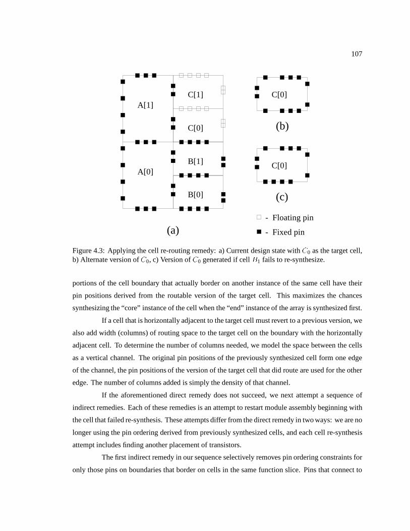
107
- Floating pin
- Fixed pin(a)
A[0]B[1]
A[1]
B[0]
C[0]
C[1] C[0]
C[0]
(b)
(c)
Figure 4.3: Applying the cell re-routing remedy: a) Current design state with C0 as the target cell,b) Alternate version of C0, c) Version of C0 generated if cell B1 fails to re-synthesize.
portions of the cell boundary that actually border on another instance of the same cell have their
pin positions derived from the routable version of the target cell. This maximizes the chances
synthesizing the “core” instance of the cell when the “end” instance of the array is synthesized first.
If a cell that is horizontally adjacent to the target cell must revert to a previous version, we
also add width (columns) of routing space to the target cell on the boundary with the horizontally
adjacent cell. To determine the number of columns needed, we model the space between the cells
as a vertical channel. The original pin positions of the previously synthesized cell form one edge
of the channel, the pin positions of the version of the target cell that did route are used for the other
edge. The number of columns added is simply the density of that channel.
If the aforementioned direct remedy does not succeed, we next attempt a sequence of
indirect remedies. Each of these remedies is an attempt to restart module assembly beginning with
the cell that failed re-synthesis. These attempts differ from the direct remedy in two ways: we are no
longer using the pin ordering derived from previously synthesized cells, and each cell re-synthesis
attempt includes finding another placement of transistors.
The first indirect remedy in our sequence selectively removes pin ordering constraints for
only those pins on boundaries that border on cells in the same function slice. Pins that connect to
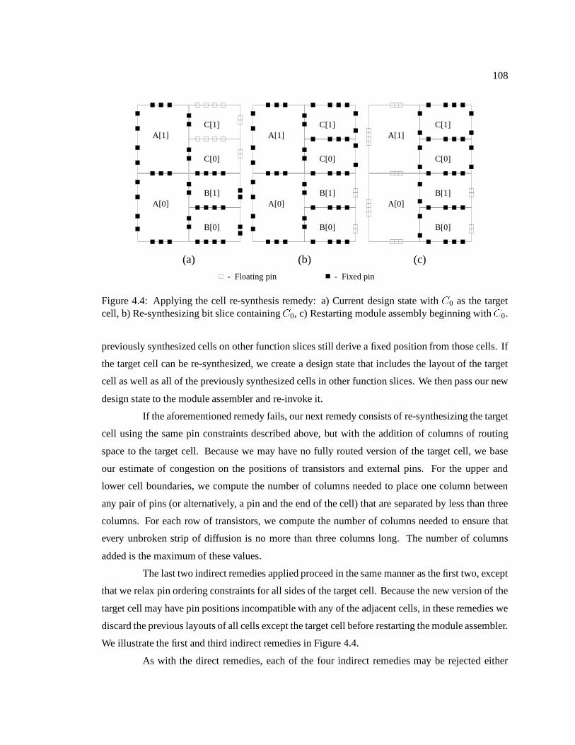
108
- Floating pin
(a)
A[0]B[1]
A[1]
B[0]
C[0]
C[1]
A[0]B[1]
A[1]
B[0]
C[0]
C[1]
A[0]B[1]
A[1]
B[0]
C[0]
C[1]
- Fixed pin
(b) (c)
Figure 4.4: Applying the cell re-synthesis remedy: a) Current design state with C0 as the targetcell, b) Re-synthesizing bit slice containingC0, c) Restarting module assembly beginning withC0.
previously synthesized cells on other function slices still derive a fixed position from those cells. If
the target cell can be re-synthesized, we create a design state that includes the layout of the target
cell as well as all of the previously synthesized cells in other function slices. We then pass our new
design state to the module assembler and re-invoke it.
If the aforementioned remedy fails, our next remedy consists of re-synthesizing the target
cell using the same pin constraints described above, but with the addition of columns of routing
space to the target cell. Because we may have no fully routed version of the target cell, we base
our estimate of congestion on the positions of transistors and external pins. For the upper and
lower cell boundaries, we compute the number of columns needed to place one column between
any pair of pins (or alternatively, a pin and the end of the cell) that are separated by less than three
columns. For each row of transistors, we compute the number of columns needed to ensure that
every unbroken strip of diffusion is no more than three columns long. The number of columns
added is the maximum of these values.
The last two indirect remedies applied proceed in the same manner as the first two, except
that we relax pin ordering constraints for all sides of the target cell. Because the new version of the
target cell may have pin positions incompatible with any of the adjacent cells, in these remedies we
discard the previous layouts of all cells except the target cell before restarting the module assembler.
We illustrate the first and third indirect remedies in Figure 4.4.
As with the direct remedies, each of the four indirect remedies may be rejected either
109
because the indicated re-synthesis of the target cell fails or because restarting the module assembler
beginning with the target cell does not result in more cells finishing synthesis than were present
in the previous design state. After each remedy is applied and rejected, the failure handler makes
a special record of whether the remedy was in fact rejected because of failure to re-synthesize the
target cell.
If the current design state remains incomplete after all indirect remedies have been applied,
the handler will pass the current best design state to the component of the failure handler that alters
external net routing. Before making this transfer, we reduce the maximum wiring capacity metric
for the cell. This represents a final effort to make the target cell routable by forcing a reduction in
the number of external wires passing through it. The reduction is accomplished via the exclusion
template mechanism described in the layout database section.
We use the aforementioned record of re-synthesis attempts on the target cell to determine
in which direction the capacity reduction will be applied. Here we distinguish three cases. If the
target cell was able to be re-synthesized during one of the first two remedies (i.e. with fixed pins for
all previously synthesized cells in other function slices), we reduce wiring capacity in the vertical
direction. If the target cell was re-synthesized only during application of the last two remedies, we
reduce the horizontal capacity of the cell. Lastly, if the target cell was not re-synthesized at all,
we make our adjustment in the direction of greatest congestion. In all cases, we make the capacity
reduction large enough so that the current wiring in that direction will exceed the new capacity of
the cell by one.
Because our primary objective in applying the aforementioned remedies has been to finish
the layout, it is possible for the completed layout to contain constraint violations, even when the
failure handler assisted in finishing the layout. In particular, this condition may arise because
width was added to a particular cell to get it to route with previously synthesized function slices
(e.g. the second indirect remedy available was successfully applied). For this condition, the only
remedy available is to re-start module assembly again from scratch and beginning with the cell that
originally had width added to it1. This corresponds to applying the third remedy in the sequence
applied to incomplete layouts, we apply it once to each cell that had width added to it. This remedy
may also be applied to reducing the net-length of the module, albeit with limited effect. Reducing
the width of the module only reduces horizontal net-length, and only a fraction (typically one-half)
of a cell’s wiring is in that direction.
1This is also tracked by the failure handler
110
A further application of re-synthesis remedies to complete layouts involves adjusting the
dimensions of the module by creating different shapes for control cells. For instance, if a module
is too tall, we attempt to reduce its height by re-synthesizing the control cell(s) in the tallest bit
slice to make them shorter but wider. The width increase allowed for the new cells is determined
by the amount of slack in the width constraint for the module and the number of function slices this
remedy must be applied to (i.e. the number of function slices with the tallest height).
We first attempt this re-synthesis as a direct remedy, i.e. we use the pin positions from
each cell’s previous version. If that fails to sufficiently reduce the module height, we next attempt
to re-synthesize the control cell(s) closest to the data block. In this remedy, for each cell in the
target function slice, only those pins that connect to other function slices retain fixed positions. We
apply this remedy at most twice, once for the cell just above and below the data block. A similar
re-synthesis sequence is applied to create taller yet thinner control cells in those (relatively rare)
cases where the widest cell in a function slice is a control cell rather than a data cell.
The set of remedies described above does not cover all possible constraint violations that
may occur in completed layouts. For instance, other than the width reduction remedy described
above, we have no remedy in this component of the failure handler that can reliably reduce module
net-length. This is partly due to the fact that, when re-synthesizing a cell, there exists no layout
attribute that can be traded off to reduce net-length. Thus, in many cases constraint violations will
remain in complete layouts after all re-synthesis remedies have been tried. These layouts are passed
to the global routing component of the failure handler.
4.2.3 Handling Global Routing Failures
The re-synthesis remedies described in the previous sub-section do modify the module’s
external wiring to the extent that external pins may assume any synthesizable order and position
along the cell boundary. However, we have found that these remedies are not especially effective
when dealing with failures directly associated with module wiring (i.e. single external net too long,
total module net-length too great, or insufficient external wiring capacity in a cell). To handle
these types of failures, we have developed a separate failure handling component that may re-route
external wires to any suitable location in the module.
As was the case with module assembly failures, we assign top priority to finishing the
global routing task in cases where the routing is incomplete. We consider the global task if any
combination of the constraint violations listed below is present in the current design state:
111
� One or more nets do not have a global routing.
� The global routing of one or more nets exceeds its length constraint.
� The global routing exceeds the wiring capacity of one or more cells.
Only the first violation listed above is produced directly by failure of the global router;
the latter two occur in design states that are passed to this component from the module assembly
failure handler. Net-length constraints occur only because adding width to a cell during re-synthesis
increases the length of nets that traverse the cell horizontally. Similarly, a cell boundary will be
overloaded only because the module assembly component of the failure handler reduced the cell’s
wiring capacity.
Regardless of where these violations originated, our first remedy involves re-invoking
the global router in attempt to route (or, if the net is too long, re-route) all nets that violated
constraints. To this end, we rip-up (i.e. remove the global routing of) all nets that exceeded their
length constraint. To give the global router some flexibility in selecting new routes, we also rip-up
all nets that are “irregular”, i.e. all nets that have pins in three or more separate bit slices and three or
more separate function slices. The remaining nets are allowed to keep their original global routing.
Recall from Chapter 3 that, because our global router works on one net at a time, nets
routed later face a more capacity constrained module than nets routed earlier. We thus give highest
weight (i.e. top priority in re-routing) to those nets that are not routed in the current design state.
Next in priority are those nets that did route but exceeded their length constraint, while the irregular
nets that did route within constraints are last to be routed in the re-invocation. This re-shuffling
of the net routing order is designed to maximize the chances of routing nets that did not route
originally, thereby undoing the effects of net ordering in the previous global router invocation.
This invocation of the global router is applied as an indirect remedy. If the previous design
state contained a cell whose wiring capacity was overloaded, we unconditionally accept the design
state that results from re-invoking the global router. Otherwise, we choose the state with the greatest
the number of routed nets. In this evaluation, nets in the previous design state that exceeded their
length constraint are counted as not having been routed.
If any nets still have not been routed, we next attempt to create sufficient space for the
unrouted nets. Our approach to adding routing space is to explicitly re-route nets that are passing
through cells to the outside of them. Our objective is to displace nets in ways that open straight
paths through the congested region inside the bounding box of each unrouted net.
112
We begin by examining unrouted nets whose bounding box contains regions of congestion
due to vertically routed nets. Our re-routing operation attempts to place one of these vertical nets
into one of the two regions immediately to the left or right of the function slice it is currently passing
through. For each bounding box, we examine each vertical net (or set thereof) that passes through
the congested region, beginning with nets nearest the center of the unrouted net’s bounding box and
working outward.
When a net is displaced, all of the connections made to cells now enter from the left or
right side of a cell rather than from the top or bottom. Thus, a net can only be displaced if the
left (or right) boundary of each cell to which it connects has enough room. Since this horizontal
connection is “local” (i.e. it does not traverse a cell), it may use the space in the center of the row
reserved for connections between adjacent cells. A vertical net also must have sufficient slack in its
length constraint to allow these horizontal connections; this is estimated to be one-half the width of
each cell to which it connects.
This stage succeeds if at least one path is found for each unrouted net and fails if we
find a region for which no net can be displaced because of its length constraint. However, in most
situations we have found that it is a lack of wiring capacity at the left or right boundaries of cells
that prevents nets from being displaced to create paths. We resolve this interdependency in space
allocation by computing every distinct2 combination of cell capacity reductions that will allow a
net to be displaced. Although for arbitrary wiring patterns the number of such combinations can be
quite large, in regular modules this number is manageable. This is because most nets in function
slices connect to the same set of bit slices and few nets span more than one function slice.
The aforementioned cell locations are combined with the cells whose congestion blocks
potential horizontal (i.e. left to right) paths for unrouted nets. Together, these locations guide the
selection of nets for vertical displacement.
The procedure for displacing nets up or down differs from horizontal (i.e. left/right)
displacement in several ways. Because space between bit slices may be added only in the large
increment of a row, our approach is to add rows in as few locations as possible and then displace
nets large distances to fill up the empty row. Connections to cells are no longer local but must cross
several intervening cells as well. Typically, there isn’t enough vertical capacity in each cell to allow
these connections to pass through them. Thus, the connections are made by a vertical segment that
runs alongside the cell combined with a horizontal local jog into the cell. Here we are free to choose
2A combination is distinct if and only if it is not a superset of another combination.
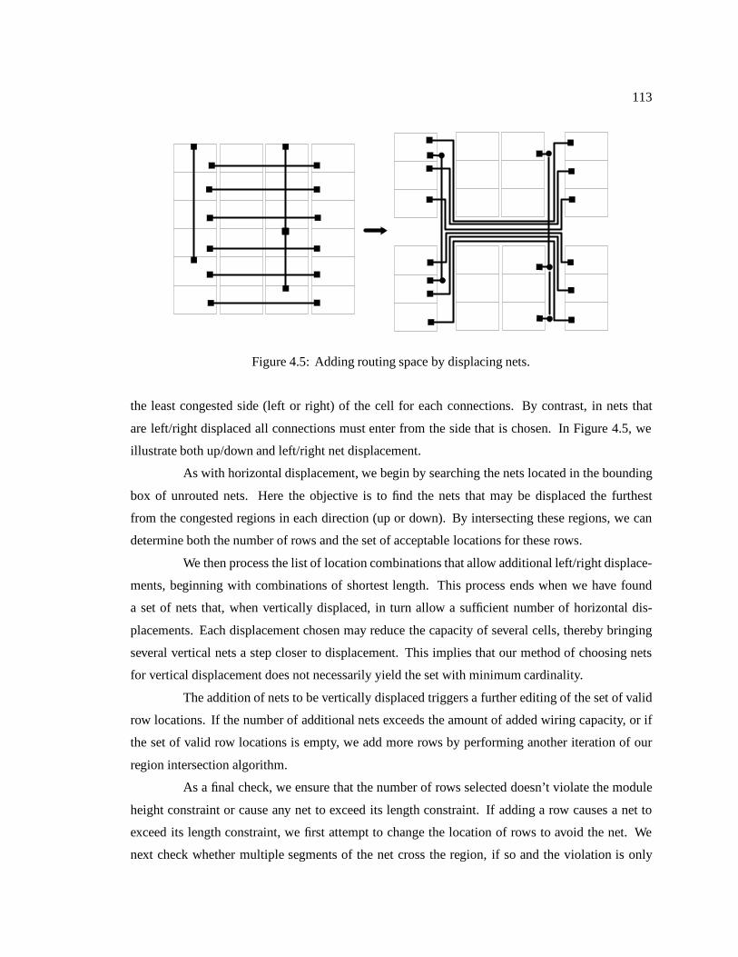
113
Figure 4.5: Adding routing space by displacing nets.
the least congested side (left or right) of the cell for each connections. By contrast, in nets that
are left/right displaced all connections must enter from the side that is chosen. In Figure 4.5, we
illustrate both up/down and left/right net displacement.
As with horizontal displacement, we begin by searching the nets located in the bounding
box of unrouted nets. Here the objective is to find the nets that may be displaced the furthest
from the congested regions in each direction (up or down). By intersecting these regions, we can
determine both the number of rows and the set of acceptable locations for these rows.
We then process the list of location combinations that allow additional left/right displace-
ments, beginning with combinations of shortest length. This process ends when we have found
a set of nets that, when vertically displaced, in turn allow a sufficient number of horizontal dis-
placements. Each displacement chosen may reduce the capacity of several cells, thereby bringing
several vertical nets a step closer to displacement. This implies that our method of choosing nets
for vertical displacement does not necessarily yield the set with minimum cardinality.
The addition of nets to be vertically displaced triggers a further editing of the set of valid
row locations. If the number of additional nets exceeds the amount of added wiring capacity, or if
the set of valid row locations is empty, we add more rows by performing another iteration of our
region intersection algorithm.
As a final check, we ensure that the number of rows selected doesn’t violate the module
height constraint or cause any net to exceed its length constraint. If adding a row causes a net to
exceed its length constraint, we first attempt to change the location of rows to avoid the net. We
next check whether multiple segments of the net cross the region, if so and the violation is only
114
the length of the “extra” segments, we rip-up that net. Otherwise, we reduce the number of rows
added to that needed exclusively for horizontal congestion relief. If the number of rows cannot be
lowered, or the reduction fails to remove the violation, the remedy terminates.
If a module height constraint is violated, our only recourse is to attempt the control re-
synthesis described in the previous sub-section. Otherwise, we must reduce the number of rows as
in the case for the net-length constraint.
If all checks are passed, the new design state becomes input to a new invocation of the
global router. Regardless of whether or not all nets are now routed, the results are passed to a
post-processing stage in which we replace nets which were originally re-routed. This replacement
attempts to reduce module width and the length of nets that exceed their constraint because of
space created between function slices. The post-processing stage does not attempt to resolve any
interdependencies in the replacement, we simply move one net at a time. We emphasize regions
where nets have their length constraint exceeded, we look at horizontal nets first because they are
most likely to have two or more vertical segments passing through the region. We then look at
vertical nets passing through these regions, returning to horizontal nets if all net-length constraints
are satisfied but the module is still too wide or tall. This post-processing step is also applied to all
completed global routings that violate any of these constraints, and it is the only remedy applied to
this state.
If no constraint violations remain, the design state is passed to the module assembly stage,
otherwise it is passed to the component that handles floor planning failures. Before handing a design
state to the failure handler, we make some alterations that reflect the information we have gathered
regarding constraint violations. For instance, if unrouted nets are present in the current design state,
we use exclusion templates to reduce the capacity of each cell that is full and is in the bounding box
of said net.
When the source of a constraint violation cannot be narrowed down to a cell, we adjust
the constraints given to the floor planner to compensate for the underestimation. For instance, in
cases where adding routing space causes violations of the module width and/or height constraint, we
simply subtract from the current constraint the amount by which the constraint was violated. This
adjustment is also used for net-length constraint violations; the amount of the adjustment depends
on whether the net was in fact routed. For unrouted nets, we simply subtract from the constraint the
amount by which the current bounding box of the net exceeds it. For routed nets, we also multiply
the previous constraint by the ratio of the bounding box length of the net to its routed length. We
then choose whichever value is smaller than the current constraint; if both values are smaller we
115
take their maximum.
4.2.4 Handling Floor Planning Failures
In the previous two components of the failure handler, our failure handling strategy has
served to augment the heuristic algorithms used in the corresponding synthesis steps. This approach
is not appropriate for handling failures in the floor planner, because the floor planner algorithm is
exact in the sense that all relative placements and shapes are included in the search space.
For design states that represent complete floor plans that violate constraints, and for
states received from the global routing failure handling component3 our remedy is to search for a
new floor plan. Because all adjustments in objective constraints made to the design state involve
tightening constraints, floor plans that were previously selected for routing and module assembly
and subsequently rejected need not be searched again. Thus, we must re-invoked the floor planner
to find those floor plans that had higher cost than the ones already selected. Such floor plans are
stored in the floor planner’s internal data structure as partial solutions. Because the queue of partial
solutions is large and required a long time to compute, we preserve it by suspending rather than
terminating the floor planner process when it is not active.
Because the floor planner search stage can apply any constraint in its evaluation of (partial)
solutions, we may pass the design state directly to the floor planner without any pre-processing.
However, the floor planner may not be able to simply resume execution using the existing queue
of partial solutions if the estimates of cell metrics on which the queue ordering was based have
changed. Currently, the only changes that require this adjustment are changes made to the estimated
width of cells. This adjustment is accomplished by the floor planner via the width adjustment
algorithm described in Chapter 3.
If the design state does not represent a complete floor plan (i.e. the floor planner did not
finish), our only recourse is to attempt to expand the floor planner’s search space. One method we
have found to accomplish this is to extend the range of floor plan shapes available. We do this by
extending the basic shape finding algorithm described in Chapter 3 by introducing the ability to
generate non-uniform bit slices. In turn, said bit slices allow us to generate datapaths whose bit
slices each process n bits in cases where the total number of bits processed by the module (N ) is
not an even multiple of n. To do this, we must add to the existing block of bit slices a bit slice
(or combination thereof) that processes the “remainder” bits (i.e. processes N mod n bits). When
3Because the global routing failure handling component doesn’t undo any portion of the placement, these states maybe considered equivalent.
116
available, we use information about the relative placement of bit slices to select bit slices that are
on the edges of the module for this alteration.
Initially, we enforce the constraint that the new bit slices be no wider than the cells in the
main block, and we only look at aspect ratios for which this condition is most likely to hold. For
instance, if a module is to process fifteen bits and we wish to have the main block consists of cells
that are three rows tall and process two bits, then when querying the layout database for cells for the
“remainder” bit slice we will ask for cells that are two rows tall and process one bit. Only if such
a cell cannot be synthesized (or the module height constraint would be violated) will we consider
cells with one row per bit. In all cases, the sum of cell widths (i.e. the width of the bit slice) must
be narrow enough to satisfy the module’s width constraint.
If all of the cells for the new shape can be synthesized by the cell, we will re-invoke the
floor planner. Because the net-list of the module has been altered, the failure handler will terminate
the floor planner process, causing it to begin again from scratch. No special processing is needed
to cause the floor planner to build floor plans with the new shape; the presence of the synthesized
cells in the layout database is sufficient.
4.3 Results
The design mediator plays an integral role in our layout system, and its work is reflected
in the results presented in Chapter 3. To isolate its effects, we must therefore analyze the details of
how the datapath results in Chapter 3 were obtained.
For instance, we have found that the floor plan chosen in Chapter 3 and illustrated in
Figure 3.8 was not the first complete solution found by the floor planner. Said solution, illustrated in
Figure 4.6, appeared first because it has a lower external net-length than the solution in Figure 3.8.
However, the cell synthesis step performed by the floor planner just before global routing revealed
that the cells associated with this solution had a higher internal net-length than originally estimated.
In particular, the shifter’s internal net-length increases greatly when all three external connection
must go to one side, and the added congestion due to external wires passing through the multiplexor
increased its net-length as well. As described in Chapter 3, this added net-length increment is used
by the floor planner as a bound for a continued search of the queue of partial solution. It is this
search step that yielded the final placement.
Looking specifically at failure handling policies, we have found that their most pronounced
effect is to increase the system’s ability to produce complete layout by reducing the dependence
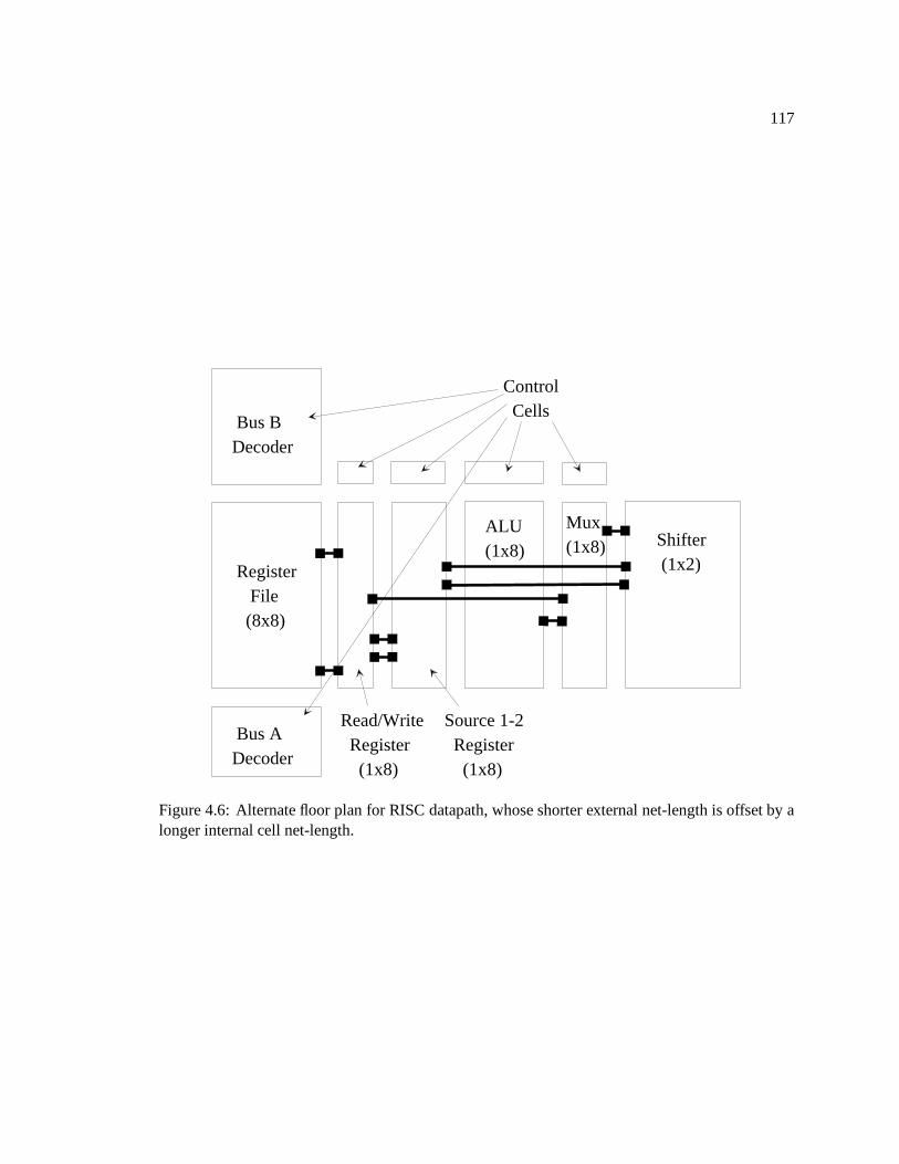
117
Register File (8x8)
Bus ADecoder
Bus BDecoder
Shifter (1x2)
Mux(1x8)
ALU(1x8)
Read/Write Register (1x8)
Source 1-2 Register (1x8)
Control Cells
Figure 4.6: Alternate floor plan for RISC datapath, whose shorter external net-length is offset by alonger internal cell net-length.

118
of the module assembler on the order in which cells are chosen for synthesis. Looking at the six
layouts presented in Chapter 3 (three shapes for two kinds of templates), we found that only two of
them, namely the layouts with a height of one row per bit, could be completed without intervention
from the failure handler. Of the remaining four cases, three were resolved by re-synthesizing the
register file and shifter function slices while adding width to them was sufficient to complete module
assembly. In all cases, the added width was needed to resolve congestion due to vertical nets. In
the remaining case, namely the dense gate isolation template layout with three rows per two bits,
synthesis halted with the shifter cell, and the layout could only be completed by employing the
indirect remedy of restarting module assembly with this cell. Applying this remedy allowed the
shifter to reverse the order of one pair of pins on one bus, and this was sufficient to complete the
layout.
We also observed that, in one layout, namely the loose gate isolation template with a three
rows per two bits height, module assembly will not complete when the shifter is chosen as the first
cell to be synthesized. Thus, simply changing the heuristic that chooses an initial cell for module
assembly does not necessarily resolve order dependence problems.
Recall that in Chapter 3 we adjusted the template height to guarantee that all external
wiring would be routed inside the cells. This precludes the failure handler from employing the
remedy of adding rows of space to accommodate horizontal external nets. To exercise this portion
of the failure handler, we generated new versions of our datapath layouts using templates with two
fewer free tracks than the values given given in Table 3.3. We found that layouts with added rows
have a larger area (7 to 12 percent) despite the use of shorter templates. This is because the decrease
in template height due to shorter templates is offset by the added width needed for local connections
and by the fact that not all added rows could be completely filled with wires.
Unfortunately, we were not able to exercise all portions of the failure handler either by
varying template height or by artificially generating datapath net-lists in the manner described in
Chapter 3. For instance, despite the need to add width to several cells, we were unable to reduce the
width of the module by using the left/right displacement of vertical nets. This is because most of the
vertical nets in our example either connect to two adjacent bit slices or to all cells in a function slice.
The former type of net isn’t long enough to benefit from displacement, and the latter requires too
many horizontal local connections. Also, the effects of pin ordering on module assembly are limited
for pins that are on sides parallel to the transistor rows (i.e. left and right sides). A full evaluation of
this effect would require datapath net-lists with non-uniform bit slices and/or complicated control
cells. We were not able to find any actual datapath examples that contained these kinds of circuits.
119
A further consequence of this is that we are unable to determine conclusively whether a strictly
greedy acceptance criterion for remedies is sufficient to find all favorable design paths.
120
Chapter 5
Summary and Conclusions
Most existing layout systems address tool interdependency issues indirectly through the
development and improvement of specific algorithms. Wherever possible, the interfaces between
tools are made as simple as possible, even at the expense of making the tools at each end of the
interface more complicated.
Inspired by the non-sequential way in which human designers tackle several layout tasks
in parallel when trying to optimize a particular layout, we have created a prototype layout system that
permits us to study different interaction strategies and communication mechanisms. This system
achieves the high degree of tool interaction necessary to perform the layout synthesis of regular
macro-modules in the Sea-of-Gates layout style.
Our system overcomes the limitations of previous automated methods for the layout of
regular macro-modules (i.e. cell assemblers) by implementing a general and flexible layout model.
To implement this model, the floor planner in our system must decide not only the relative placement
of function blocks that minimizes the wiring among them but also the alignment and aspect ratio
for each block that maximizes the amount of wiring that can be routed by abutment. Because
the external wiring passes through each cell, the floor planner must also ensure that the external
wiring load through each cell is distributed such that its layout can be completed. To fully use this
flexibility, our algorithms for floor planning and external net routing are designed to accommodate
an arbitrary degree of non-regularity in the module, yet are optimized for regular modules.
The floor planner makes use of the SoGOLaR[46] cell generator to provide customized
cell layouts at the transistor level to match particular aspect and pin position constraints. SoGOLaR
uses a flexible placement strategy where transistors are first grouped into P/N pairs and then placed
on a symbolic grid using a cost function that takes into account both diffusion sharing and wiring
121
length. This approach eliminates the need for any hierarchy in the transistor net-list, and is flexible
enough to accommodate different styles of Sea-of-Gates templates. We have used this flexibility to
obtain data on the tradeoffs involved in selecting different styles of Sea-of-Gates templates.
The synthesis elements of our system are bound together by a separate component for
handling inter-tool communication and design path control. The communications mechanism allows
communication among all the layout synthesis task components and also provides a database of
layout attempts in which both successful and failed layouts are stored. Because the number of
potential design states is not large, our layout database uses simple algorithms for storage and
retrieval.
Our approach to design path control is to intervene in the “normal” sequential design
path for the module (i.e. floor planning, external net routing, cell assembly) only when one of the
aforementioned tasks cannot complete, or the result does not meet the specified constraints. Our
method of failure handling can either “patch” or, if necessary, gracefully roll back layouts that fail
to meet specified constraints. The handler selects remedies using a “greedy” approach that requires
far less storage and is far more goal-directed than standard backtracking. As such, our approach
represents an intermediate point (in terms of flexibility and complexity) between a strictly sequential
layout process and performing layout with a general set of peer agents with no model specifying
the order in which they should be called.
Unfortunately, in the design and implementation of remedies we were unable to exploit the
full generality afforded by our communications mechanism. For instance, we found it very difficult
to design remedies that move directly from a late stage in module layout (i.e. module assembly)
to an early one (i.e. floor planning). Similarly, almost all meaningful exchanges of feedback
information occurred between tools that are adjacent to one another in the normal sequential design
process. Furthermore, the remedies that were used most often in our system were local remedies
that apply to a single cell. Lastly, we have found that the design of remedies, while not tied to
the specific implementation of the synthesis tools, are in fact influenced by the properties of the
synthesis algorithms.
Despite this apparent limitation, we believe our approach represents a useful method for
organizing a group of interacting design synthesis tools. In developing an explicit representation
of items to be communicated, and an explicit approach to failure handling, one can confront the
most important issues related to tool interaction while not precluding creative methods of resolving
them. Although we have used the relatively simple design domain of VLSI layout to demonstrate its
feasibility, we believe our approach would prove even more valuable in design domains that contain
122
a wider variety of synthesis approaches, objectives, evaluation methods and design concerns.
123
Bibliography
[1] A. R. Newton. Computer-Aided design of VLSI circuits. Proceedings of the IEEE,
69(10):1189–1199, October 1981.
[2] M. Stefik, D. G. Bobrow, A. Bell, H. Brown, L. Conway, and C. Tong. Thew partitioning
of concerns in digital systems design. In Proceedings on Advanced Research in VLSI, pages
43–52, January 1982.
[3] Institute of Electrical and Electronics Engineers, Piscataway, New Jersey. IEEE Standard
VHDL Reference Manual, first edition, 1987.
[4] Neil Weste and Kamran Eshraghian, editors. Principles of Custom VLSI Design. Addison
Wesley Publishing Company, 1985.
[5] Bryan T. Preas and Michael J. Lorenzetti, editors. Physical Design Automation of VLSI
Systems, chapter 7. The Benjamin/Cummings Publishing Company, Inc., 1988.
[6] H. Fleisher and L. I. Maissel. An introduction to array logic. IBM Journal of Research and
Development, 19(2):98–109, March 1975.
[7] G. DeMicheli and A. M. Sangiovanni-Vincentelli. Multiple constrained folding of pro-
grammable logic arrays, theory and practice. IEEE Transactions on Computer-Aided Design,
CAD-2(2):151–167, 1983.
[8] A. Weinberger. Large scale integration of MOS complex logic: A layout method. IEEE
Journal of Solid-State Circuits, SC-2(4):182–190, December 1967.
[9] A. Lopez and H. Law. A dense gate matrix layout method for MOS VLSI. IEEE Transactions
on Electronic Devices, ED-27(8):1671–1675, 1980.

124
[10] D. G. Baltus and Jonathan Allen. SOLO: A generator of efficient layouts from optimized MOS
circuit schematics. In Proc. 25th Design Automation Conf., pages 445–452, June 1988.
[11] Neil Weste and Kamran Eshraghian, editors. Principles of Custom VLSI Design, chapter 8.
Addison Wesley Publishing Company, 1985.
[12] Bryan T. Preas and Michael J. Lorenzetti, editors. Physical Design Automation of VLSI
Systems, chapter 1. The Benjamin/Cummings Publishing Company, Inc., 1988.
[13] Neil Weste and Kamran Eshraghian, editors. Principles of Custom VLSI Design, chapter 5.
Addison Wesley Publishing Company, 1985.
[14] Michael R. Garey and David S. Johnson. Computers and Intractability: A Guide to the Theory
of NP-Completeness. W. H. Freeman and Company, 1979.
[15] Bryan T. Preas and Patrick G. Karger. Automatic placement: A review of current techniques.
In Proc. 25th Design Automation Conf., pages 622–628, June 1986.
[16] B. Kernighan and S. Lin. An efficient heuristic procedure for partitioning graphs. Bell System
Technical Journal, 49(2):291–307, February 1970.
[17] Bryan T. Preas and Michael J. Lorenzetti, editors. Physical Design Automation of VLSI
Systems, chapter 4. The Benjamin/Cummings Publishing Company, Inc., 1988.
[18] D. D. Hill. Sc2D: A broad-spectrum automatic layout system. In Proceedings IEEE 1987
Custom Integrated Circuits Conference, pages 729–732, May 1987.
[19] A. E. Dunlop and B. W. Kernighan. A procedure for layout of standard-cell VLSI circuits.
IEEE Transactions on Computer-Aided Design, CAD-4(1):92–98, January 1985.
[20] P. R. Suaris and G. Kedem. Quadrisection: A new approach to standard cell layout. In
Proceedings ICCAD-87, Nov. 1987.
[21] M. Burstein and R. Pelavin. Hierarchical wire routing. IEEE Transactions on Computer-Aided
Design, CAD-2(4):223–234, October 1983.
[22] A. M. Patel, N. L. Soong, and R. K. Korn. Hierarchical VLSI routing- an approximate routing
procedure. IEEE Transactions on Computer-Aided Design, CAD-4(2):121–126, 1985.
125
[23] A. Hashimoto and J. Stevens. Wire routing by optimizing channel assignment within large
apertures. In Proc. 8th Design Automation Conf., pages 155–163, 1971.
[24] C. Sechen and A. Sangiovanni-Vincentelli. The Timberwolf placement and routing package.
In Proceedings of the 1984 Custom Integrated Circuits Conference, pages 78–85, May 1984.
[25] W. A. Christopher. Mariner: A Sea-of-Gates layout system. Master’s thesis, University of
California at Berkeley, 1989.
[26] M. Burstein, S. J. Hong, and R. Pelavin. Hierarchical VLSI layout: Simultaneous placement
and wiring of gate arrays. In Proceedings of the International Conference of VLSI, pages
45–60, August 1983.
[27] R. S. Tsay, E. S. Kuh, and C.-P. Hsu. PROUD: A fast sea-of-gates placement algorithm. In
Proceedings of the 25th Design Automation Conference, pages 318–323, 1988.
[28] J. M. Kleinhans, G. Sigl, and F. M. Johannes. GORDIAN: A new global optimization /
rectangle dissection method for cell placement. In Proceedings ICCAD-88, pages 506–510,
1988.
[29] Bryan T. Preas and Michael J. Lorenzetti, editors. Physical Design Automation of VLSI
Systems, chapter 5, pages 170–181. The Benjamin/Cummings Publishing Company, Inc.,
1988.
[30] D. P. LaPotin and S. W. Director. Mason: A global floorplanning approach for VLSI design.
IEEE Transactions on Computer-Aided Design, CAD-5(4):477–489, October 1986.
[31] Wei Ming Dai and E. S. Kuh. Simultaneous floor planning and global routing for hierarchical
building block layout. IEEE Transactions on Computer-Aided Design, CAD-6(5):828–837,
September 1987.
[32] R. H. J. M. Otten. Automatic floorplan design. In Proceedings of the 19th Design Automation
Conference, pages 261–267, 1982.
[33] D. M. Schuler and E. G. Ulrich. Clustering and linear placement. In Proc. 9th Design
Automation Conference, pages 50–56, June 1972.
126
[34] B. Eschermann, Wei Ming Dai, E. S. Kuh, and M. Pedram. Hierarchical placement for
macrocells: A “meet in the middle” approach. In Proceedings ICCAD ’88, pages 460–463,
1988.
[35] R. Muller. A new approach for simultaneous floorplanning and global wiring. Methods of
Operations Research, (62):287–289, 1990. No volume number given.
[36] M. Ohmura, S. Wakabayashi, Y. Toyohara, J. Miyao, and N. Yoshida. Hierarchical floor-
planning and detailed global routing with routing-based partitioning. In Proceedings of the
International Symposium on Circuits and Systems, pages 1640–1643, 1990.
[37] P.-S. Tzeng and C. H. Sequin. Codar: A congestion-directed general area router. In Proceedings
ICCAD-88, Nov. 1988.
[38] P.-S. Tzeng. Integrated Placement and Routing for VLSI Layout Synthesis and Optimization.
PhD thesis, University of California at Berkeley, 1992.
[39] B. D. N. Lee. Combined Hierarchical Approaches to Integrated Circuit Layout Based on a
Common Data Model. PhD thesis, University of California at Berkeley, 1993.
[40] David L. Johannsen. Silicon Compilation. PhD thesis, California Institute of Technology,
1981.
[41] C. S. Bamji, C. E. Hauck, and J. Allen. A design by example regular structure generator. In
Proc. 22nd Design Automation Conference, pages 16–22, 1985.
[42] S. Law and J. D. Mosby. An intelligent composition tool for regular and semi-regular structures.
In Proc. ICCAD-85, pages 169–171, Nov. 1985.
[43] R. N. Mayo. Mocha Chip: a system for the graphical design of VLSI module generators. In
Proc. ICCAD-86, pages 74–77, November 1986.
[44] M. Ishikawa and T. Yoshimura. A new module generator with structural routers and a graphical
interface. In Proc. ICCAD-87, pages 436–439, 1987.
[45] D. P. Dutt and G. Lakhani. Optimization for automatic cell assembly. In Proc. Intl. Conf. on
Computer Design, pages 186–189, April 1988.
[46] G. D. Adams and C. H. Sequin. Template style considerations for sea-of-gates layout genera-
tion. In Proc. 26th Design Automation Conf., pages 31–36, June 1989.
127
[47] T. Uehara and W.M. VanCleemput. Optimal layout of CMOS functional arrays. IEEE Trans-
actions on Computers, C-30(5):305–312, 1981.
[48] R. L. Masiasz and J. P. Hayes. Layout optimization of CMOS functional cells. In Proc. 24th
Design Automation Conf., pages 544–551, June 1987.
[49] D. D. Hill. Sc2: A hybrid automatic layout system. In Proceedings ICCAD-85, pages 172–174,
1985.
[50] S. Wimer, R. Y. Pinter, and J. Feldman. Optimal chaining of CMOS transistors in a functional
cell. IEEE Transactions on Computer-Aided Design, CAD-6(5):795–801, 1987.
[51] T. A. Hughes, R. Salama, and W. Liu. BBC: A module generator for back-to-back cells. In
Proc. ICCAD-86, pages 440–443, Nov. 1987.
[52] S. Kirkpatrick, C.D. Gelatt Jr., and M.P. Vecchi. Optimization by simulated annealing. SCI-
ENCE, 220(4298):671–680, 1983.
[53] N. Metropolis, A. Rosenbluth, M. Rosenbluth, A. Teller, and E. Teller. Equation of state
calculations by fast computing machines. Journal of Chemical Physics, 21:1087–1092, 1953.
[54] B. Gidas. Non-stationary Markov chains and the convergence of the annealing algorithm.
Journal of Statistical Physics, 39:73–131, 1985.
[55] C. Sechen and A. Sangiovanni-Vincentelli. The Timberwolf placement and routing package.
IEEE Journal of Solid-State Circuits, SC-20(2):510–522, April 1985.
[56] A. Casotto, F. Romeo, and A. Sangiovanni-Vincentelli. A parallel simulated annealing algo-
rithm for the placement of macro-cells. In Proc. ICCAD-86, pages 30–33, 1986.
[57] Srinivas Devadas and A. Richard Newton. GENIE: a generalized array optimizer for VLSI
synthesis. In Proceedings 23rd Design Automation Conference, pages 631–637, 1986.
[58] A. Stauffer and R. Nair. Optimal CMOS cell transistor placement: A relaxation approach. In
Proc. ICCAD-88, pages 364–367, 1988.
[59] S. R. White. Concepts of scale in simulated annealing. In Proceedings of the International
Conference on Computer Design, pages 646–651, 1984.
128
[60] M. D. Huang, F. Romeo, and A. Sangiovanni-Vincentelli. An efficient general cooling schedule
for simulated annealing. In Proc. ICCAD-86, pages 381–384, 1986.
[61] C.-L. Ong, J.-T. Li, and C.-Y. Lo. GENAC: an automatic cell synthesis tool. In Proceedings
26th Design Automation Conference, pages 239–243, June 1989.
[62] L. Layer. Analysis of Sea-of-Gates template and cell library design issues. Master’s thesis,
University of California at Berkeley, 1987.
[63] P. Duchene and M. J. Declerq. A highly flexible Sea-of-Gates structure for digital and analog
applications. IEEE Journal of Solid-State Circuits, 25(5):576–584, June 1989.
[64] M. Beunder, J. Kernhof, and B. Hoefflinger. Effective implementation of complex and dynamic
CMOS logic in a gate forest environment. In Proceedings of the Custom Integrated Circuits
Conference, pages 44–47, May 1987.
[65] P. Birzele and P. Michel. Reduced Design and Manufacturing Time by New Semicustom
Standards and VLSI-Design Methodologies. Siemens AG, March 1987.
[66] Masatashi Kawashima, Makoto Takechi, Kunihiko Izuzaki, Kuniaki Kishida, Kazuo Itoh,
Minoru Fujita, Toshiyuki Nakao, and Ikuro Masuda. An 18K 1 �m CMOS gate array with
high testability structure. In Proceedings of the Custom Integrated Circuits Conference, pages
52–55, May 1987. Three pairs with N/P gates tied together, separate rows of unconnected N
and P for transmission gates.
[67] F. Anderson and J. Ford. A 0.5 micron 150K channelless gate array. In Proceedings of the
Custom Integrated Circuits Conference, pages 35–38, May 1987. Four P/N pairs, three of
which have pre-connected gates.
[68] A. Hui, A. Wong, C. Dell’Oca, D. Wong, and R. Szeto. A 4.1K gates double metal HCMOS
Sea-of-Gates array. In Proceedings of the Custom Integrated Circuits Conference, pages
15–17, May 1985. Plain vanilla gate isolation.
[69] C. P. Hsu. Automatic layout of channelless gate array. In Proceedings of the Custom Integrated
Circuits Conference, pages 281–284, May 1986. A four transistor cell with Power/ground in
the middle of each diffusion zone!

129
[70] R. Brayton, E. Detjens, S. Krishna, T. Ma, P. McGeer, L.-F. Pei, N. Phillips, R. Rudell, R. Segal,
A. Wang, R. Yung, and A. Sangiovanni-Vincentelli. Multiple-level logic optimization system.
In Proceedings ICCAD-86, November 1986.
[71] D. Curry. Schematic specification of datapath layout. In Proceedings of ICCD, pages 28–34,
1989.
[72] H. Cai, S. Note, P. Six, and H. DeMan. A data path layout assembler for high performance
DSP circuits. In Proc. 27th Design Automation Conference, pages 306–311, 1990.
[73] C l. Cheng and C y. Ho. SEFOP: a novel approach to data path module placement. In
Proceedings Custom Integrated Circuits Conference, pages 9.5.1–9.5.5, 1993.
[74] M. Trick and S. W. Director. LASSIE: structure to layout for behavioral synthesis tools. In
Proceedings 26th Design Automation Conference, pages 104–109, 1989.
[75] M. Hiersch and D. Siewiorek. Automatically extracting structure from a logical design. In
Proc. ICCAD-88, pages 456–459, 1988.
[76] G. Odawara, T. Hiraide, and O. Nishina. Partitioning and placement technique for CMOS gate
arrays. IEEE Transactions on Computer-Aided Design, CAD(6):355–363, 1987.
[77] Y. Tsujihashi, H. Matsumoto, S. Kato, H. Nakao, O. Kitada, K. Okazaki, and H. Shinohara. A
high density datapath generator with stretchable cells. In Proceedings IEEE Custom Integrated
Circuits Conference, pages 11.3.1–11.3.4, 1992.
[78] Christos H. Papadimitriou and Kenneth Steiglitz. Combinatorial Optimization: Algorithms
and Complexity, pages 438–444. Prentice-Hall Inc., 1982.
[79] H. Nakao, O. Kitada, M. Hayashikoshi, K. Okazaki, and Y. Tsujihashi. A high density
datapath layout generation method under path delay constraints. In Proceedings IEEE Custom
Integrated Circuits Conference, pages 9.5.1–9.5.4, 1993.
[80] J m. Ho, G. Vijayan, and C.K. Wong. Constructing the optimal rectilinear steiner tree derivable
from a minimum spanning tree. In Proc. ICCAD-89, pages 6–9, 1989.
[81] C. Lee. An algorithm for path connections and its applications. IRE Transactions on Electronic
Computers, VEC(10):346–365, 1961.
130
[82] A. B. Cohen and M. Shechory. Track assignment in the pathway datapath layout assembler.
In Proc. ICCAD-91, pages 102–105, November 1991.
[83] B. Ackland, A. Dickenson, R. Ensor, J. Gabbe, P. Kollaritsch, T. London, C. Poirier, P. Sub-
rahmanyam, and H. Watanabe. CADRE - A system of co-operating VLSI design experts. In
Proceedings of ICCD ’85, pages 99–104, 1985.
[84] Y-L. Steve Lin and D. D. Gajski. LES: A layout expert system. In Proc. 24th Design
Automation Conference, pages 672–678, 1987.