Embed Size (px)
Citation preview

by George Marsh
Predictions that Moore’s law – which states that the
number of components fabricated on a chip will
double every 18 months – is about to come up
against a physical ‘red brick wall’ seem perennial. But
optical lithographers have so far confounded the
prophets of doom, managing to etch ever finer
details onto Si. Now, though, the limits are truly in
sight, leaving chip makers wondering what
technology can carry them forward towards the
billion-transistors-on-a-chip mark and whether a
successor will finally be needed for complementary
metal oxide semiconductor (CMOS). The likely
answer to these questions may appear surprising.
Photolithography is still working wonders for the chip
industry. Not so long ago, moving from the 248 nm
laser wavelength standard and the 120 nm features
that it can routinely produce to a 193 nm laser
wavelength and 90 nm features seemed a big
challenge. Yet, even as chip makers adopt this new
standard and consider enhancing it through two or
three generations to produce features of 60 nm and
less, lithographic tool makers are starting to gear up
for 157 nm deep ultraviolet (DUV) technology as the
next step. Predictions are that 10 GHz microprocessor
clock speeds, compared with the present 2.8 GHz
state-of-the-art, should be achieved by 2006.
But, because of fundamental physical limitations, that is
about as far as conventional optical lithography can in
improving resolution by reducing the imaging wavelength.
A wavelength of 157 nm, generated by fluorine lasers, is
already at the UV edge of the visible spectrum and moving
beyond this takes us into the realm of vacuum UV and
X-rays. As current lens materials are opaque at these
wavelengths, existing optical techniques may no longer have
anything to contribute. Conventional wisdom says that
patterning at a scale of only a few tens of nanometers
requires completely new technologies utilizing electron or ion
beams. However, the discovery that there is a band in the
‘soft’ X-ray region (2-50 nm) amenable to techniques still
recognizably optical, suggests that the boundaries of this
type of lithography can be pushed back yet again. Some
argue that this band, better termed extreme UV (EUV) for
chip technology purposes, may not only render 157 nm
Moore’s lawat the extremes
May 200328 ISSN:1369 7021 © Elsevier Science Ltd 2003
INSIGHT FEATURE
photolithography (and a 126 nm successor proposed in some
quarters as a ‘last gasp’ for optically-based technology)
unnecessary, but could even take us all the way to the
natural limits of CMOS-based computing, where leakage and
other phenomena occurring between transistor elements
might disrupt normal electronic functioning.
The first suggestions that EUV lithography (EUVL) could
viably extend Moore’s law came in 19881,2. Groups from the
Lawrence Livermore National Laboratory (LLNL) and Bell Labs
succeeded in applying reflected EUV rays in projection
lithography systems at 4.5 nm and 37 nm, respectively. They
relied on large synchrotron sources to create the required
soft X-ray beams and used grazing incidence reflection.
Within a year, researchers at the Nippon Telephone and
Telegraph LSI Laboratories in Japan provided the first
demonstration of EUVL imaging using normal incidence,
multilayer-coated optics. Utilizing 13 nm radiation, this work
yielded 0.5 µm features3. However, it was Bell Labs who first
demonstrated the true potential of the technique in 1990.
With 13 nm radiation, Bell researchers achieved 0.05 µm
features on a PMMA (poly [methyl methacrylate]) resist4 –
the detail resolution being in line with the general rule that
features can be realized to about half of the light wavelength
used. The following year, Sandia National Laboratories took
matters further, demonstrating the first EUVL imaging system
in which a compact laser, rather than a synchrotron, was the
radiation source5. Five years after that, Sandia produced the
first workable device able to achieve EUVL patterning, using a
microstepper developed in conjunction with Bell6.
Up to this point the technique had been known as ‘soft
X-ray projection lithography’, but the name was changed to
EUVL to avoid confusion with proximity X-ray lithography.
Unfortunately, the US Department of Energy, which had been
the main source of funding for this work, withdrew its
support as a result of changes in government priorities during
the mid-1990s. But, so promising were the results, a
consortium of IC manufacturers including Intel, Motorola, and
Advanced Micro Devices decided to sponsor LLNL, Sandia, and
the Lawrence Berkeley National Laboratory (LBNL). The three
labs refer to themselves as the Virtual National Laboratory
(VNL). A year and a half ago, the VNL unveiled an EUVL
prototype machine with a numerical aperture of 0.1 able to
produce 70 nm features – already almost comparable to the
best obtainable with conventional optical lithography7.
According to Don Sweeney, LLNL-based chief technology
officer of the VNL, a commercialized version of the
technology should be able to support IC fabrication at 45 nm
initially, scaling through successive generations down to
22 nm without significant loss of production throughput.
Some researchers believe that the method could eventually
realize features as small as 10 nm, about the same scale as
molecular electronic devices.
All done by mirrorsThe basic geometry of an EUVL system is shown in Fig. 1.
Light from a 13.5 nm source is reflected from a patterned
mask and imaged with a four-times reduction onto a
photoresist-coated wafer via a series of mirrors.
Central to the EUVL ‘magic’ is the use of mirrors in place
of transmissive lenses within the beam focusing optics. This is
because all known lens materials absorb these soft X-ray
frequencies. The mirrors must be slightly off-axis so as not to
obscure the light path and require carefully computed
nonspherical shapes to maintain sharp focusing. Although
functionally similar to optical mirrors, those used in EUVL are
physically very different and construction is a major
challenge. To achieve useful levels of reflectance, they rely on
multiple reflections occurring at different levels within a
multilayer stack made up of alternate layers of Mo and Si.
These are deposited by magnetron sputtering, electron beam,
or evaporation techniques. More than 80 layers have been
used in experimental systems to yield some 70% reflectance
overall. So that the individual reflections are additive, layers
need to be of a precise thickness – 2.8 nm for Mo and 4.1 nm
for Si. Because of reflectance losses at each mirror, designers
May 2003 29
Reflectivemask
Absorberpattern
Multilayermirror
Wafer torecord 0.1 µmfeatures orsmaller, overcm2 dimensions
4:1reductionoptics,aspheric,multilayercoated
λ = 13 nm
Fig. 1 Schematic of the EUVL system. The light source, along with the associatedcondenser, is not shown. The system requires a four-times reduction camera (for clarityonly two mirrors are shown), a patterned reflective mask, and an EUV-sensitive resist.
must work with as few optical surfaces as possible and
cannot rely on further mirrors to correct aberrations. Instead,
corrections are accommodated within the very specific
shapes of the aspheric mirror surfaces. The VNL’s prototype
camera system has just four mirrors with a numerical
aperture of 0.1, but commercial systems will probably have
six mirrors and a numerical aperture of 0.25. (Resolution
scales directly with numerical aperture.)
Producers of commercially viable demagnifying EUV optics
will have to meet stringent requirements for these mirrors
and the multilayer structure. Standards for the IC industry’s
45 nm node dictate that etched lines do not vary by more
than ~5 nm and are placed on the photoresist mask to within
~15 nm. To meet these requirements, multilayer thickness
over the entire optics must be held to within one part in
5000 and the pass bands of the multilayers should match to
within 0.01 nm. Mirror substrates must be polished, typically
by ion bombardment, with extremely low error levels. The
mirror surfaces in the VNL’s prototype system are finished to
within 0.1-0.2 nm rms over clear aperture dimensions of
50-150 nm. Geometric shape errors for the assembled system
should not exceed 0.4 nm rms. As well as complying with
these tolerances, the multilayer material must be stable and
durable so that commercial EUV optical systems can last at
least five to ten years in service.
Achieving these parameters reliably is difficult, particularly
given the limitations of existing polishing and metrology
tools. Only visible wavelength interferometry methods are
powerful enough to support fabrication of the mirror shapes.
Once fabricated, the mirrors must be mounted and aligned
relative to each other in a stable manner. The mounts
themselves and the distortion effects of gravity must all be
taken into account. Changing the orientation of the mirrors
relative to gravity will deform the mirrors many times
beyond the required specifications. Only the most
sophisticated computer-based designs and control methods
allow the system to be assembled and maintained.
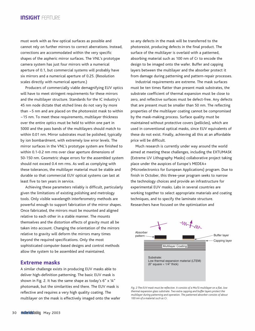
Extreme masksA similar challenge exists in producing EUV masks able to
deliver high-definition patterning. The basic EUV mask is
shown in Fig. 2. It has the same shape as today’s 6” x ¼”
photomask, but the similarities end there. The EUV mask is
reflective and requires a very high quality coating. The
multilayer on the mask is effectively imaged onto the wafer
so any defects in the mask will be transferred to the
photoresist, producing defects in the final product. The
surface of the multilayer is overlaid with a patterned,
absorbing material such as 100 nm of Cr to encode the
design to be imaged onto the wafer. Buffer and capping
layers between the multilayer and the absorber protect it
from damage during patterning and pattern-repair processes.
Industrial requirements are extreme. The mask surfaces
must be ten times flatter than present mask substrates, the
substrate coefficient of thermal expansion must be close to
zero, and reflective surfaces must be defect-free. Any defects
that are present must be smaller than 50 nm. The reflecting
properties of the multilayer coating cannot be compromised
by the mask-making process. Surface quality must be
maintained without protective covers (pellicles), which are
used in conventional optical masks, since EUV equivalents of
these do not exist. Finally, achieving all this at an affordable
price will be difficult.
Much research is currently under way around the world
aimed at meeting these challenges, including the EXTUMASK
(Extreme UV Lithography Masks) collaborative project taking
place under the auspices of Europe’s MEDEA+
(Microelectronics for European Applications) program. Due to
finish in October, this three-year program seeks to narrow
the technology choices and provide an infrastructure for
experimental EUV masks. Labs in several countries are
working together to select appropriate materials and coating
techniques, and to specify the laminate structure.
Researchers have focused on the optimization and
INSIGHT FEATURE
May 200330
Absorberpattern Buffer layer
Capping layer
Substrate:Low thermal expansion material (LTEM)(6" square × 1/4" thick)
Multilayer Coating
Fig. 2 The EUV mask must be reflective. It consists of a Mo/Si multilayer on a flat, lowthermal expansion glass substrate. Two extra capping and buffer layers protect themultilayer during patterning and operation. The patterned absorber consists of about 100 nm of a material such as Cr.

INSIGHT FEATURE
industrialization of evaporation and electron-beam coating of
surfaces for both optics and masks. Related work involving
Carl Zeiss, Philips Research, and lithography toolmaker ASML,
for instance, has been aimed at optimizing ion beam energies,
incidence angles, and other polishing settings. Angular scan
reflectivity monitoring systems are being developed so that
high coating consistency can be achieved from one run to
another. Hard X-ray, diffractometry, reflectrometry, photo-
electron spectroscopy, and EUV microscopy tools are also
being utilized to secure multilayer quality.
A criticism leveled by supporters of competing
technologies, such as electron-beam lithography, is that such
sandwich structures will be difficult to repair. For example,
techniques will be required to repair opaque defects in the
absorber material at the multilayer surface. Using focused ion
beams for local defect removal is an obvious approach, but
risks damaging the multilayer. One possible solution is to
incorporate a thin C layer as a buffer to prevent ions from
penetrating below the surface. Researchers have verified,
both theoretically and experimentally using secondary ion
mass spectroscopy, that a 25 nm layer effectively bars the
passage of most ions, making ion beam removal of opaque
mask defects feasible.
PhotoresistsEUVL photoresists are basically the same as those currently
used for DUVL. To date, therefore, most research has focused
on surveying existing DUV resists. One difference, though, is
that the resists absorb EUV light fairly readily so that they
have to be thinner than for DUV. A typical layer thickness is
100-130 nm, about a fifth of a DUV equivalent. Modifications
to DUV resists require formulations to obtain coatings of this
thickness.
Resists acceptable for high-volume manufacture must
exhibit good resolution, high contrast for printing, good etch
resistance, a sensitivity of ~5 mJ/cu•cm, and low outgassing.
A resist must also address the line edge roughness that has
become an increasing problem for fine-detail lithographies.
Three basic approaches are under investigation: silylated
single-layer resists, ultra-thin single layer resists on top of a
refractory hard mask, and bilayer resists. Regardless of the
approach, the active imaging layer must be only ~100 nm.
All significant results presented to date (including those
shown in Fig. 5) have used the ultra-thin single layer
structure. A photoresist of 100 nm is coated on top of a hard
mask of a material such as SiO2. The ultra-thin resist is
exposed to EUV radiation and wet-developed. The pattern in
the developed photoresist is transferred to the hard mask
using a dry etchant. Finally, the hard mask provides a robust
etch mask for transfer to the IC device.
Resists produced to date have a resolution of about
50 nm. This will have to be improved as EUVL moves from
the 45 nm node down to the 22 nm node. Research into
improved resists meeting all the required specifications is
gaining momentum. The necessary experimental facilities
with high resolution (i.e. numerical aperture) imaging test-
beds will be coming on-line within a year.
EUVL sourcesA powerful, compact, and reliable source of 13.5 nm light is
felt to be the most challenging requirement of EUVL.
Synchrotron sources used in the early 1990s generate X-ray
light by emission from electrons. They are, however, large,
expensive, and produce radiation that is too coherent.
Moderate-temperature plasmas (20-100 eV) also emit X-ray
radiation and are regarded as the most promising option.
Plasmas can be produced electrically – by z-pinch, capillary
discharge, hollow cathode discharge, or plasma focus – or by
pulsed laser irradiation of a target material. Schematics of
two options are shown in Fig. 3. In a typical laser-produced
plasma (LPP) system for EUVL, a pulsed Nd:YAG laser is
focused onto a jet of Xe gas to produce a gas plasma. Light at
13.5 nm, emitted as part of the blackbody radiation from this
plasma, can then be collected optically (by a condenser), and
passed onto the reflective mask.
The engineering of sources suitable for commercial
application have been well elucidated by, among others,
researchers from the Royal Institute of Technology in
Stockholm, Sweden8. Probably the greatest difficulty is
attaining 13.5 nm emission of sufficient power at the resist
without damaging the condenser optical system. Lithographic
tool manufacturers such as Canon, Nikon, and ASML estimate
that 50-150 W within a 2% bandwidth of 13.5 nm would
have to be collected by the condenser for a viable production
tool. These power levels are sufficient for a lithographic
throughput of about a hundred 300 mm wafers per hour.
Achieving this with an LPP source requires lasers of high
power and pulse repetition rate, with significantly improved
efficiency in converting drive power to in-band EUV radiation.
To date, efficiency levels have been low – typically ~1%.
May 2003 31

Xe is currently the plasma source of choice for both
discharge and LPP sources because its generation results in
little debris to contaminate the condenser optical mirrors. For
LPP, contamination can be reduced by ensuring that the
plasma is formed away from the nozzle through which the Xe
jet is ejected. Experiments have been carried out with various
forms of debris mitigation, but none have been completely
successful to date. Conversion efficiencies are being tackled
through attention to Xe jet parameters and stability,
optimization of pulse/plasma interaction, trials of different
pulsing techniques, and improving condenser design.
Of the ten or so research efforts in progress worldwide to
develop EUV sources, the current status is about 10 W of in-
band EUV light collected by the condenser – a factor of about
ten less than required.
Working prototypeAn engineering test stand (ETS), effectively a prototype EUVL
system, developed by the VNL offers the best indication yet that
this ‘extreme lithography’ technique can be made to work at the
industrial level (Fig. 4). The system comprises an LPP source with
a 1500 W laser, a four-element condenser, a reflective mask, and
a four-mirror 0.1 numerical aperture imaging system. This entire
system must be operated in a vacuum because EUV light is
absorbed by air. The ETS, with its vacuum system, occupies a
3 m x 3 m x 4 m high enclosure, which is itself kept in a
cleanroom to exclude possible contaminants. A collage of
images produced with the ETS is shown in Fig. 5.
As described earlier, the mask is produced by patterning an
absorber material deposited onto a multilayer-coated, low
thermal expansion mask blank. The required pattern image is
reproduced on the wafer at a quarter of the original scale by
step-and-scan technology similar to that used in today’s
DUVL tools. A high-precision control system governs the
initial die alignment, mask and wafer position control at each
stage, and exposure and focus setting during stage scanning.
The ETS demonstrated full-field sub-100 nm imaging soon
after it first became operational in 2001. This represented an
INSIGHT FEATURE
May 200332
Fig. 4 Engineering drawing of the ETS prototype tool built by the VNL. The tool includes anEUV source, a condenser illumination system, a four-times reduction projection opticalsystem, a patterned reflective mask, and an EUV-sensitive resist on a wafer. Associatedsubsystems include focus systems, scanning mask and wafer stages, optics housing, waferand reticle handling interfaces, vacuum and thermal management systems, and robotics.
Fig. 3 There are two basic approaches for commercial EUVL sources, both involving emission from a 20-100 eV plasma. (a) Laser-produced plasma source: the plasma is usually producedin a liquid or a gas to avoid debris. (b) Electrical discharge plasma source. While discharge is the more efficient of the two methods, it generates more harmful debris and much excessenergy in a small space, which must be removed.
(a) (b)

INSIGHT FEATURE
encouraging alpha class capability and supported much early
EUVL system learning. The optical imaging system has a
figure error of 0.7 nm (50 milliwaves) rms and a flare of 20%.
Although commercial systems will have to double both figure
and flare, the ETS values are considered an impressive first
demonstration. Fig. 5 shows dense and isolated lines, along
with contacts down to 70 nm. In a commercial tool with a
higher numerical aperture, a 70 nm feature would scale to
28 nm. The process windows for the ETS show that depth of
focus for 100 nm dense lines is a full micron.
ProspectsClearly, technical challenges remain. Foremost among them
are high power source development and the production of
defect-free masks at commercially acceptable costs of
ownership. Additionally, there are always advocates of
competing technologies. Only time will tell how this will play
out in the marketplace.
The construction and operation of the ETS to demonstrate
EUVL technology has been funded by Extreme Ultraviolet
LLC, an Intel-led consortium that includes five other chip
makers. The next critical phase is for EUVL to leave the
research environment and move into the commercial
marketplace. In 2002, the first beta tool orders were
placed with commercial suppliers, for intended delivery
in 2006. Commercial requirements call for a tool to
support the 45 nm node by the year 2007 and EUVL is
expected to support CMOS IC manufacturing through the
22 nm node.
As a result, an Excellence in Technology Transfer award
has been made to the EUVL team at the VNL. According to
the awarding body, the Federal Laboratory Consortium, the
team has successfully transferred the technology to the
private sector. “Much work remains to be done before
EUVL is ready to be a cost-effective method for IC
manufacturing,” says Sweeney, “but all the pieces are in
place and I am confident that industry can complete the
process. The push for commercialization marks another
phase of what, I believe, offers the best hope, of several
candidate technologies, for extending the potential for
CMOS beyond what anyone could have foreseen a few years
ago. It should lead to microprocessors that are tens of times
faster than today’s most powerful chips, together with
memory chips having storage capacity to match.” If
Sweeney’s hopes, along with those of growing cohorts of
researchers around the world, are fulfilled, EUVL could help
give Moore’s law and CMOS a much needed ten-year life
extension. MT
AcknowledgmentsThe author gratefully acknowledges the help of Don Sweeney in preparing this article andfor supplying illustrative material.
May 2003 33
REFERENCES
1. Hawryluk, A. M., and Seppala, L. G., J. Vac. Sci. Technol. B (1988) 66 (6), 2162
2. Silfvast, W. T., and Wood II, O. R., Microelectron. Eng. (1988) 88 (1-2), 3
3. Kinoshita, H., et al., J. Vac. Sci. Technol. B (1989) 77 (6), 1648
4. Bjorkholm, J. E., et al., J. Vac. Sci. Technol. B (1990) 88 (6), 1509
5. Tichenor, D. A., et al., Opt. Lett. (1991) 1166 (20), 1557
6. Nguyen, K. B., et al., In: OSA TOPS on Extreme Ultraviolet Lithography, Kania,D., and Kubiak, G. D., (eds.), Optical Society of America, Washington, (1996), 44
7. Sweeney, D. W., et al., EUV optical design for a 100 nm CD imaging system. In: Emerging Lithographic Technologies, SPIE, (1998) 33333311, 2
8. Hansson, B. A. M., et al., Liquid-Xenon Jet Laser Plasma Source for EUVLithography. Proc. SPIE, (2001) 44550066
Fig. 5 A collage of images produced by the ETS. The images are top-down scanningelectron micrographs of the developed photoresist.