Embed Size (px)
Citation preview
MICROCONTROLLER BASE FULL BRIDGE FORWARD
POWER SUPPLY UNIT
MUHAMAD AZIZAN BIN MAT SIRAT
This thesis is submitted as partial fulfillment of the requirements for the
award of the Bachelor of Electrical Engineering (Hons.) (Power Systems)
Faculty of Electrical & Electronics Engineering
Universiti Malaysia Pahang
OCTOBER, 2008

ACKNOWLEDGEMENT
In the name of Allah, The Most Loving and The Most Compassionate
I would like to take this opportunity to extend my deepest gratitude to the
following persons who helped me a lot in this project, which enabled me to complete
my research project in time as a partial of the requirement for the Bachelor of Electrical
Engineering (Power Systems).
First and foremost, a special thank to my supervisor En. Mohammad Fadhil bin
Abas, who helped me a lot for the project research, for all the support, continuous
patience, and supervision given throughout the project.
I would like to give my appreciation to Mr. Mohd Azlan bin Sayuti for his
valuable time spent in giving his authority to use his laboratory. His laboratory helped
me in doing analysis and further studies for this project.
Thank you to my classmates with their encouragement and help. Last but not
least, my special thanks, to my family members for their continuous support and advice
from the early stage of my studies.
ABSTRACT
Nowadays, there are many power supply unit topologies. In this project, it is
been proposed to do the full-bridge dc-dc converter topology. The full-bridge c dc-dc
converter topology was chosen for several reasons. The primary benefit of using a Full-
Bridge dc-dc converter is its power handling capabilities, stability, and symmetry.
Secondly, using a high frequency transformer is one of the most efficient ways to step
up or step down the voltage and to transfer the power to the full-wave rectifier circuit.
Basically, this topology is referred to the use of switch mode power supply (SMPS)
technique. In designing SMPS, it used high frequency transformer. The purpose of a
power transformer in Switch-Mode Power Supplies is to transfer power efficiently and
instantaneously from an external electrical source to an external load. In doing so, the
transformer also provides important additional capabilities. As mentioned just now, this
design uses the high frequency switch. Therefore, a controller is needed to control or
vary the duty cycle of PWM during switching time. In this design, PIC is chosen as the
main controller of this PSU. PIC was chosen because of ease to program the switching
time of four switches. Normally, MOSFET or IGBT is selected for the power switch.
Circuit driver is also needed to drive voltage signal from PIC to the power switches. In
this case, suitable IC driver must be used.

ABSTRAK
Dewasa kini, terdapat banyak jenis kaedah dalam menghasilkan bekalan kuasa.
Dalam projek ini, ditugaskan membuat kaedah full-bridge dc-dc converter. Kaedah full-
bridge dc-dc converter dipilih disebabkan beberapa faktor. Kelebihan utama dengan
menggunakan kaedah ini adalah kelebihan dari aspek power handling, stability, dan
symmetry. Kemudian, dengan menggunakan transformer frekuensi tinggi adalah satu
cara yang lebih efisien untuk meningkatkan atau menurunkan voltan dan memindahkan
kuasa kepada litar full-wave rectifier. Pada asasnya, kaedah ini dirujuk sebagai teknik
switch mode power supply (SMPS). Dalam menghasilkan SMPS, ia menggunakan
transformer frekuensi tinggi. Tujuan transformer frekuensi tinggi dalam SMPS adalah
untuk memindahkan kuasa secara efisien dan berterusan daripada sumber elektrik luar
kepada beban luar. Dengan cara ini, transformer juga akan membekalkan keupayaan
tambahan. Seperti yang saya jelaskan tadi, projek ini menggunakan suis berfrekuensi
tinggi. Oleh sebab itu, pengawal diperlukan untuk mengawal atau mengubah duty cycle
PWM. Dalam projek ini, PIC dipilih sebagai pengawal utama. PIC dipilih kerana ia
mudah untuk memprogramkan masa suis bagi empat suis. Kebiasaanya, MOSFET atau
IGBT dipilih untuk suis kuasa. Litar penggerak juga diperlukan untuk membawa voltan
daripada PIC kepada suis kuasa. Dalam hal ini, penggerak yang sesuai mesti digunakan.

TABLE OF CONTENTS
CHAPTER TITLE PAGE
TITLE PAGE i
DECLARATION ii
ACKNOWLEDGEMENT iii
ABSTRACT iv
ABSTRAK v
TABLE OF CONTENTS vi
LIST OF TABLES ix
LIST OF FIGURES x
LIST OF APPENDIXES xii
1 INTRODUCTION 1
1.1 Introduction 1
1.2 Objectives 3
1.3 Scope of Project 4
2 LITERATURE REVIEW 5

3 METHODOLOGY 8
3.1 Simulation Design 9
3.2 Hardware Development 9
3.2.1 Developing 9
3.2.2 Designing 12
3.3 Component Determination 17
3.3.1 Capacitor and Resistor 17
3.3.2 Bridge Rectifier 17
3.3.3 Transformer 17
3.3.4 Controller 18
3.3.5 Power Switch 18
3.3.6 Power Switch Driver 19
3.4 Software Development 19
3.4.1 Peripheral Programming 21
4 RESULT AND DISCUSSION 22
4.1 Simulation Result 22
4.2 Hardware Result 27
4.2.1 Driver Circuit Design 27
4.2.2 PIC Circuit Design 30
4.2.3 Designing High Frequency
Transformer 31
4.2.4 Designing Power Supply 35
4.2.5 Designing Circuit Feedback 35
4.2.6 Designing Full Bridge DC-DC
Converter 36

4.3 Software Design 37
4.4 Costing and Commercialization 41
5 CONCLUSION AND RECOMMENDATIONS 44
5.1 Summary of Work 44
5.2 Future Recommendations 45
REFERENCES 46
APPENDICES
APPENDIX A Sample of Full Program to Generate Two PWM
With Feedback 47
APPENDIX B Picture of Full Project 52
APPENDIX C Picture of Output Results 53

LIST OF TABLES
TABLE NO. TITLE PAGE
1 Summarize Calculation Value 16
2 Range of Voltage of Feedback Circuit 39
3 Revised Material Cost 41

LIST OF FIGURES
FIGURE NO. TITLE PAGE
1 Block Diagram of Project 9
2 A Simple Program of Generating Two PWMs 21
3 Simulated Design Circuit of the First Stage of
the Project 23
4 Simulated Design Circuit of the Second Stage of
the Project 23
5 Graph of Single Phase Supply Voltage 24
6 Graph of Input Filtering (dc supply) 24
7 Graph of Primary Voltage Transformer 25
8 Graph of Secondary Voltage Transformer 25
9 Graph of Desired Output Voltage 26
10 Driver Circuit for Half-bridge 28
11 High-side Signal 28
12 Low-side Signal 28
13 Full-bridge Driver Circuit 29
14 Square-wave Output 29
15 PIC18F4550 Circuit 30
16 Transformer Housing 31
17 Transformer Clips 31

18 Ferrite 32
19 Copper Coil (2.5A) 32
20 Black Tape 32
21 Windings are being made 33
22 Black Tape is used to provide Isolation 33
23 Inductance Measurement Meter 34
24 Power Supply 5Vdc and 15Vdc 35
25 Circuit Feedback 36
26 Full Schematics of Full Bridge DC-DC Converter
Power Supply Unit 37
27 Flow Chart of the Program 40

LIST OF APPENDICES
APPENDIX TITLE PAGE
A Sample of Full Program to Generate Two PWMs with
Feedback 47
B Picture of Full Project 52
C Picture of Output Results 53
CHAPTER 1
INTRODUCTION
1.1 Introduction
Nowadays, there are many power supply unit topologies. Among of the
topologies are buck dc-dc converter, boost dc-dc converter, buck-boost dc-dc converter,
flyback dc-dc converter, push-pull dc-dc converter, half-bridge dc-dc converter, and
full-bridge c dc-dc converter. In this project, it is proposed to do the full-bridge dc-dc
converter topology. The full-bridge c dc-dc converter topology was chosen for several
reasons. The primary benefit of using a Full-Bridge dc-dc converter is its power
handling capabilities, stability, and symmetry. Secondly, using a high frequency
transformer is one of the most efficient ways to step up or step down the voltage and to
transfer the power to the full-wave rectifier circuit. The high frequency transformer is
also much smaller and lighter than a standard 8.5 kVA 60 Hz transformer. Basically,
this topology is referred to the use of switch mode power supply (SMPS) technique.
A switched-mode power supply, switching-mode power supply or SMPS, is an
electronic power supply unit (PSU) that incorporates a switching regulator. While a
linear regulator uses a transistor biased in its active region to specify an output voltage,

an SMPS actively switches a transistor between full saturation and full cutoff at a high
rate. The resulting rectangular waveform is then passed through a low-pass filter
(typically an inductor and capacitor) to achieve an approximated output voltage.
Advantages of this method include smaller size, better power efficiency, and lower heat
generation. Disadvantages include the fact that SMPSs are generally more complex than
linear supplies, generate high-frequency electrical noise that may need to be carefully
suppressed, and have a characteristic ripple voltage at the switching frequency.
In designing SMPS, it used high frequency transformer. The purpose of a power
transformer in Switch-Mode Power Supplies is to transfer power efficiently and
instantaneously from an external electrical source to an external load. In doing so, the
transformer also provides important additional capabilities. Among of the important
additional capabilities are the primary to secondary turns ratio can be established to
efficiently accommodate widely different input/output voltage levels, multiple
secondary with different numbers of turns can be used to achieve multiple outputs at
different voltage levels, and separate primary and secondary windings facilitate high
voltage input/output isolation, especially important for safety in off-line applications.
As mentioned just now, this design uses the high frequency switch. Therefore, a
controller is needed to control or vary the duty cycle of PWM during switching time. In
this design, PIC is chosen as the main controller of this PSU. PIC was chosen because
of ease to program the switching time of four switches. Normally, MOSFET or IGBT is
selected for the power switch. Circuit driver is also needed to drive voltage signal from
PIC to the power switches. In this case, suitable IC driver must be used.

1.2 Objectives
The objective of this project:
i. To produce a high frequency power supply by using switch mode power supply
technique (SMPS). Linear power supplies use a transformer operating at the
mains frequency of 50 or 60 Hz. This low-frequency transformer is several
times larger and heavier than a corresponding transformer in an SMPS,
which runs at typical frequencies of 50 kHz to 1 MHz
ii. Provide high efficiency and less loss during switching time. A linear supply
regulates the output voltage or current by expending excess power as heat,
which is inefficient. A regulated SMPS will regulate the output using duty
cycle control, which draws only the power required by the load. In all SMPS
topologies, the transistors are always switched fully on or fully off. Thus,
ideally, SMPSs are 100% efficient. The only heat generated is in the non-
ideal aspects of the components. Switching losses in the transistors, on-
resistance of the switching transistors, equivalent series resistance in the
inductor and capacitors, and rectifier voltage drop will lower SMPS
efficiency. However, by optimizing SMPS design, the amount of power loss
and heat can be minimized. A good design can have an efficiency of 95%.
iii. Provide isolation to PSU by using high frequency transformer. All transformers
provide dc isolation between isolated windings. However, because they all
have capacitance from a winding to any nearby conductor, such as other
windings, the core, and the chassis, they can couple high frequency signals
and noise to these nearby conductors. This capacitive coupling mechanism
can carry high frequency noise on the input primary to the output secondary
windings or vice versa. Isolation transformers are designed to minimize this
coupling by construction that minimizes capacitive coupling, or by the use of
shields, or both.

iv. The designed power supply must meet the requirement that is output voltage is
30Vdc, output current at maximum 5A, and power efficiency at least 80%.
1.3 Scope of Project
Among of the scope of project are:
i. Design a rectifier circuit to produce dc output voltage from 240Vrms.
ii. Design a full-bridge power supply unit using switch mode power supply
(SMPS) technique
iii. Design a controller to control the duty cycle of pulse with modulation (PWM)
during switching time
iv. Design the high frequency transformer
CHAPTER 2
LITERATURE REVIEW
Basically, there are two types of power supply. One is linear power supply
(conventional power supply unit) and the other one is switch mode power supply
(SMPS). Switch Mode Power Supplies are the current state of the ability in high
efficiency power supplies. Conventional series-regulated linear power supplies maintain
a constant voltage by varying their resistance to cope with input voltage changes or load
current demand changes. The linear regulator can, therefore, tend to be very inefficient.
The switch mode power supply, however, uses a high frequency switch (in practice a
transistor) with varying duty cycle to maintain the output voltage. The output voltage
variations caused by the switching are filtered out by an LC filter (C J Hill, 1997).
Full-bridge dc-dc converter power supply unit topology is chosen for certain
factors. Full-bridge dc/dc converters are extensively applied in medium to high power
dc/dc power conversion. High efficiency, high power density, high reliability and low
EMI are some of the most desirable features for these converters, particularly for
computer and telecommunication applications (Dheeraj K. Jain, Praveen K. Jain and
Haibo Zhang, 2002).
Full bridge and half-bridge topologies with full bridge secondaries have the best
transformer efficiency because the core and the windings are fully utilized. With center-
tapped secondaries, winding utilization and efficiency are reduced. With center tapped
primary and secondaries, winding utilization and efficiency are further reduced. All of
the push pull topologies have the further advantage that for a given switching
frequency, giving the same output ripple filtering and closed loop capability, the
frequency at which the transformer core and windings operate is halved, reducing core
and ac winding losses (Lloyd H. Dixon, 2001).
There are three major power switch choices; the bipolar junction transistor
(BJT), the power MOSFET, and the integrated gate bipolar transistor (IGBT). The BJT
was the first power switch to be used in this field and still offers many cost advantages
over the others. It is also still use for very low cost or in high power switching
converters. The maximum frequency of operation of bipolar transistor is less than 80-
100 kHz because of some of their switching characteristics. The IGBT is used for high
power switching converters, displacing many of the BJT applications. They too, though,
have a slower switching characteristic which limits their frequency of operation to
below 30 kHz typically although some can reach 100 kHz. IGBT’s have smaller die
areas than power MOSFETs of the same ratings, which typically means a lower cost.
Power MOSFETs are used in the majority of applications due to their ease of use and
their higher frequency capabilities (ON Semiconductor, July 2002).
Before using power switches, firstly circuit driver must be constructed. To
design circuit driver, all the requirements possibility must be obeyed. Mostly, the
requirements are gate driver voltage, incoming dc voltage, incoming dc current and
input protection for the driver and the power switch. All these possibilities must be
followed to ensure the system functional and safety to be implemented.
After completing several stages, the designed high frequency transformer could
not simply connected to the MOSFET (switching). Some additional circuit must be
constructed and added between connection of MOSFET and high frequency
transformer. When the MOSFET turns off, a high-voltage spike occurs on the drain pin
because of a resonance between the leakage inductor (Llk) of the main transformer and
the output capacitor (COSS) of the MOSFET. The excessive voltage on the drain pin

may lead to an avalanche breakdown and eventually damage the MOSFET. Therefore,
it is necessary to add an additional circuit to clamp the voltage. This circuit is known as
RCD Snubber Clamp for transformer (Design RCD Snubber, 2006).
Finally, the use of microcontroller (PIC) as a main controller of the full-bridge
dc-dc converter power supply unit. PIC acts to give pulse width modulation (PWM)
signal to the power switches throughout the driver circuit. The value or the ratio of
PWM is calculated depending from desired output signal. Besides that, PIC works as a
feedback to maintain the output signal if there any overvoltage or over current to the
output.

CHAPTER 3
METHODOLOGY
There are some steps will be applied in designing a microcontroller base full-
bridge forward power supply unit. The necessary and related information have been
discovered throughout the literature review.
In this methodology, I have separated into three elements. Among of the
elements are:
i. Simulation Design
ii. Hardware Development
iii. Software Development
3.1 Simulation Design
OrCAD PSpice is chosen to simulate the circuit designed. In this
simulation, it will show the simulated output results. This simulation is very
essential to keep all theoretical design and calculation is suitable to the project
designed. Besides that, it can give clear view of the project according the
obtained simulation output.
3.2 Hardware Development
3.2.1 Developing
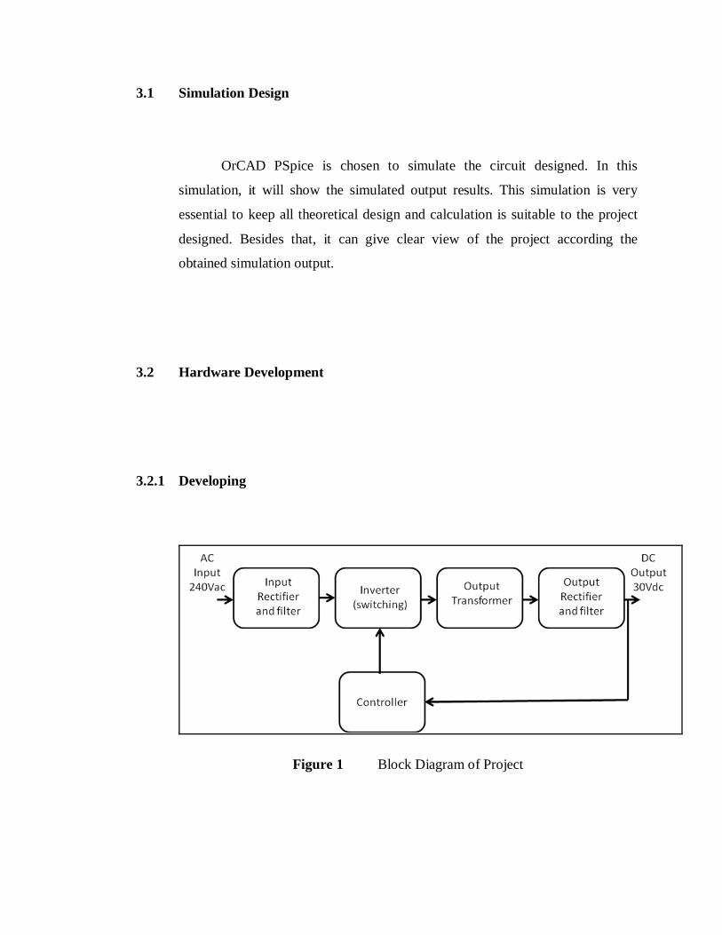
Figure 1 Block Diagram of Project
In this developing, hardware design will be constructed. From above figure, it
shows each stage for the hardware design. Among of the stages are input rectifier and
filter, inverter (switching), output transformer (high frequency transformer), output
rectifier and filter, and controller. The hardware development will be completed by
following each stages of the block diagram.
3.2.1.1 Input Rectifier and Filter
If the SMPS has an AC input, then its first job is to convert the input to DC. This
is called rectification. The rectifier circuit can be configured as a voltage doublers by
the addition of a switch operated either manually or automatically. This is a feature of
larger supplies to permit operation from nominally 240 volt supplies. The rectifier
produces an unregulated DC voltage which is then sent to a large filter capacitor.
3.2.1.2 Inverter (switching)
The inverter stage converts DC, whether directly from the input or from the
rectifier stage described above, to AC by running it through a power oscillator, whose
output transformer is very small with few windings at a frequency of tens or hundreds
of kilohertz (kHz). The frequency is usually chosen to be above 20 kHz, to make it
inaudible to humans. The output voltage is optically coupled to the input and thus very
tightly controlled. The switching is implemented as a multistage (to achieve high gain)
MOSFET amplifier. MOSFETs are a type of transistor with a low on-resistance and a high
current-handling capacity.

3.2.1.3 Output Transformer, Rectifier and Filter
If the output is required to be isolated from the input, as is usually the case in
mains power supplies, the inverted AC is used to drive the primary winding of a high-
frequency transformer. This converts the voltage up or down to the required output level
on its secondary winding. The output transformer in the block diagram serves this
purpose.
If a DC output is required, the AC output from the transformer is rectified. For
output voltages above ten volts or so, ordinary silicon diodes are commonly used. For
lower voltages, Schottky diodes are commonly used as the rectifier elements; they have
the advantages of faster recovery times than silicon diodes (allowing low-loss operation
at higher frequencies) and a lower voltage drop when conducting. For even lower output
voltages, MOSFET transistors may be used as synchronous rectifiers; compared to
Schottky diodes, these have even lower "on"-state voltage drops.
The rectified output is then smoothed by a filter consisting of inductors and
capacitors. For higher switching frequencies, components with lower capacitance and
inductance are needed.
3.2.1.4 Controller
A feedback circuit monitors the output voltage and compares it with a reference
voltage, which is set manually or electronically to the desired output. If there is an error
in the output voltage, the feedback circuit compensates by adjusting the timing with
which the MOSFETs are switched on and off. This part of the power supply is called
the switching regulator. The "controller" shown in the block diagram serves this
purpose. Depending on design/safety requirements, the controller may or may not
contain an isolation mechanism (such as opto-couplers) to isolate it from the DC output.
Open-loop regulators do not have a feedback circuit. Instead, they rely on
feeding a constant voltage to the input of the transformer or inductor, and assume that
the output will be correct. Regulated designs work against the parasitic capacity of the
transformer or coil, monopolar designs also against the magnetic hysteresis of the core.
The feedback circuit needs power to run before it can generate power, so an
additional non-switching power-supply for stand-by is added.
3.2.2 Designing
In this designing all the inputs and the outputs are identified. Theoretical design
and calculation is studied base on the project. Each component will be used for the
project is identified whether it is contented for the recommendation design or not. So,
hand calculation is needed to identify the value of each components based on the
theoretical design.

3.2.2.1 Input Rectifier and Filter
The design specification was given as follows:
Supply voltage: 240V/50Hz
Maximum power required: Po = 150W
Thus, average voltage (peak voltage)
Vp = √2 × 240V = 339.41V (3.1)
Ideal power
Pin = Pout = Prec
Prec = Vrec × Irec (3.2)
Where; Vrec = output voltage of rectifier
Irec = output current of rectifier
Therefore,
AV
W
V
P
n
n
i
i442.0
41.339
150I rec
(3.3)
Load (resistor)
99.767150
41.339
Prec
Vrec
Vrec = Prec
Irec × Vrec = Prec
22
2
R
R
(3.4)