Embed Size (px)
Citation preview
Current and Emerging
Memory Technology Landscape
Greg Atwood
Micron Technology
Flash Memory Summit 2011
Santa Clara, CA 1
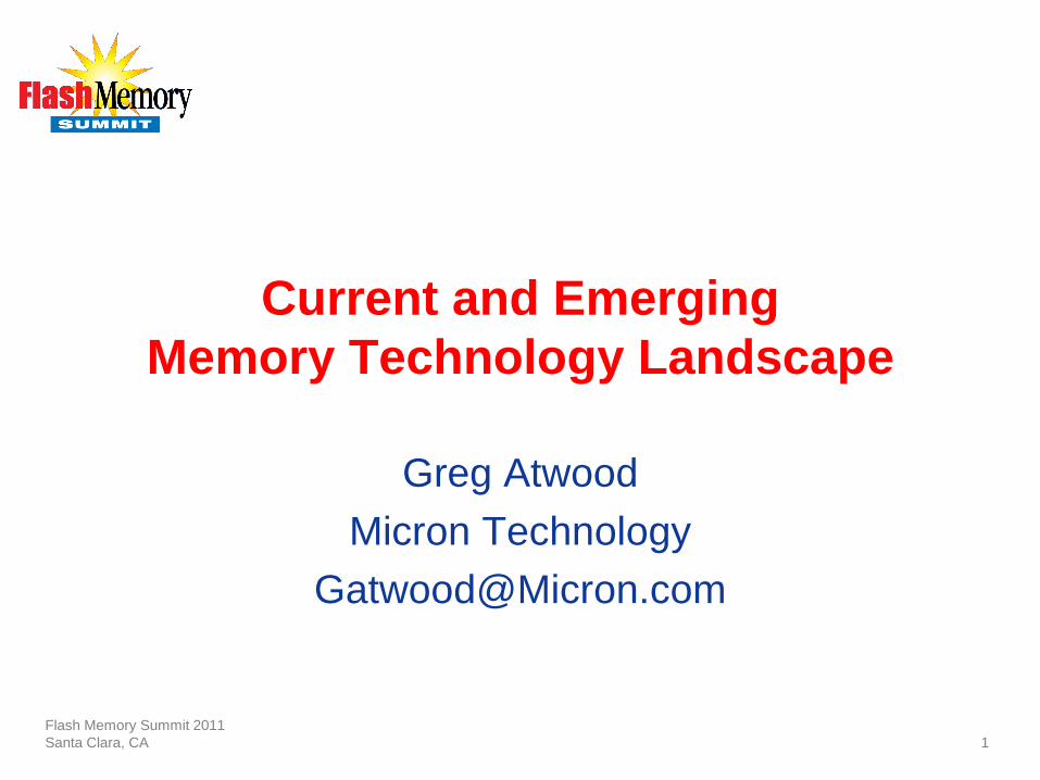
A New Era Emerging for Memory?
Convergence of many factors/pressures:
• Increasing importance of memory to user experience
Our lives are becoming one big shared database, with IOPs
becoming more important than MIPs
• Both NAND and DRAM facing scaling challenges
No hard ―wall,‖ but increasing complexity
• Explosion of ―new‖ memory storage concepts
New storage physics are enabling new usage models
• Evolving memory hierarchy
New features, relentless cost reduction, and need for I/O
performance are remaking the memory hierarchy
2
Memory is moving from a support role to a defining system role
Flash Memory Summit 2011
Santa Clara, CA
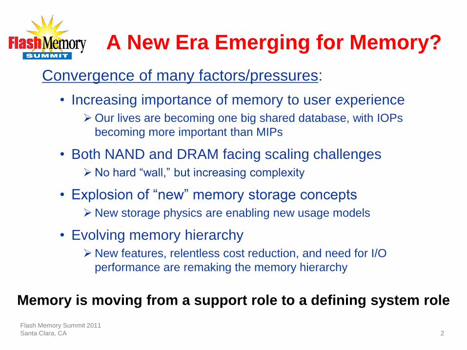
Memory-Relevant Trends
3
Cellular(Phones)
Mobile(Laptops/MIDs)
Computing(Desktops/Laptops)
Enterprise(Servers/Storage)
Consumption
Content• Performance-driven (generally I/O limited)
• “Green” focus bringing power into foreground
• Reliability vs. cost is the trade-off
• Ease of use
• Instant-on/off
• Power vs. “good enough” performance trade-off
Flash Memory Summit 2011
Santa Clara, CA
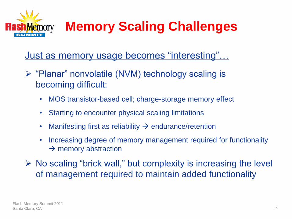
Memory Scaling Challenges
Just as memory usage becomes ―interesting‖…
―Planar‖ nonvolatile (NVM) technology scaling is
becoming difficult:
• MOS transistor-based cell; charge-storage memory effect
• Starting to encounter physical scaling limitations
• Manifesting first as reliability endurance/retention
• Increasing degree of memory management required for functionality
memory abstraction
No scaling ―brick wall,‖ but complexity is increasing the level
of management required to maintain added functionality
Flash Memory Summit 2011
Santa Clara, CA 4
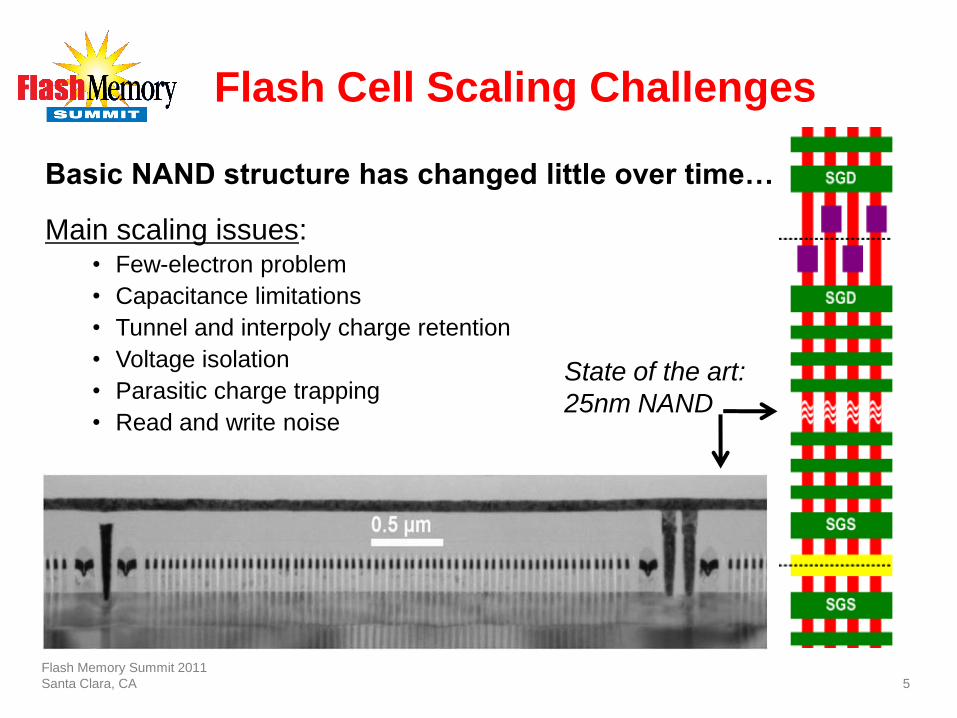
Flash Cell Scaling Challenges
5
Basic NAND structure has changed little over time…
Main scaling issues:• Few-electron problem
• Capacitance limitations
• Tunnel and interpoly charge retention
• Voltage isolation
• Parasitic charge trapping
• Read and write noise
State of the art:
25nm NAND
Flash Memory Summit 2011
Santa Clara, CA
0
10
20
30
40
50
60
0 10
20
30
40
50
60
70
80
90
100
Nu
mb
er
of
ele
ctr
on
s f
or
a
100m
V V
Tsh
ift
Feature size (nm)
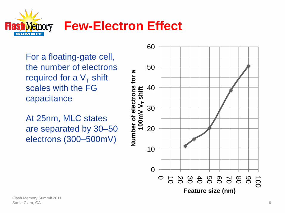
Few-Electron Effect
For a floating-gate cell,
the number of electrons
required for a VT shift
scales with the FG
capacitance
At 25nm, MLC states
are separated by 30–50
electrons (300–500mV)
Flash Memory Summit 2011
Santa Clara, CA 6
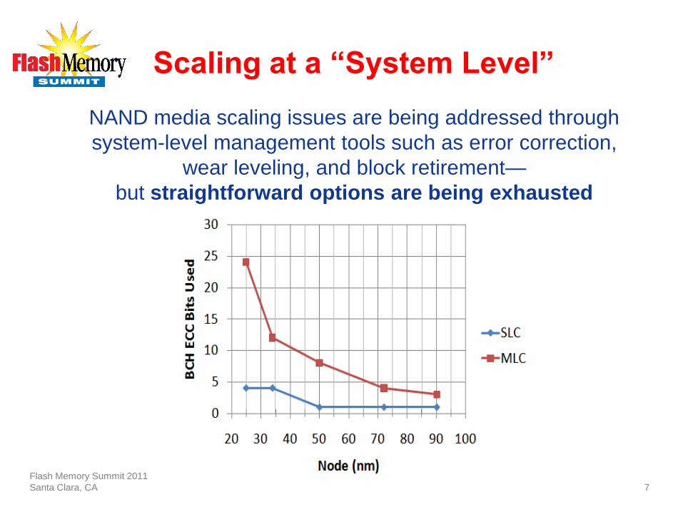
Scaling at a “System Level”
NAND media scaling issues are being addressed through
system-level management tools such as error correction,
wear leveling, and block retirement—
but straightforward options are being exhausted
Flash Memory Summit 2011
Santa Clara, CA 7
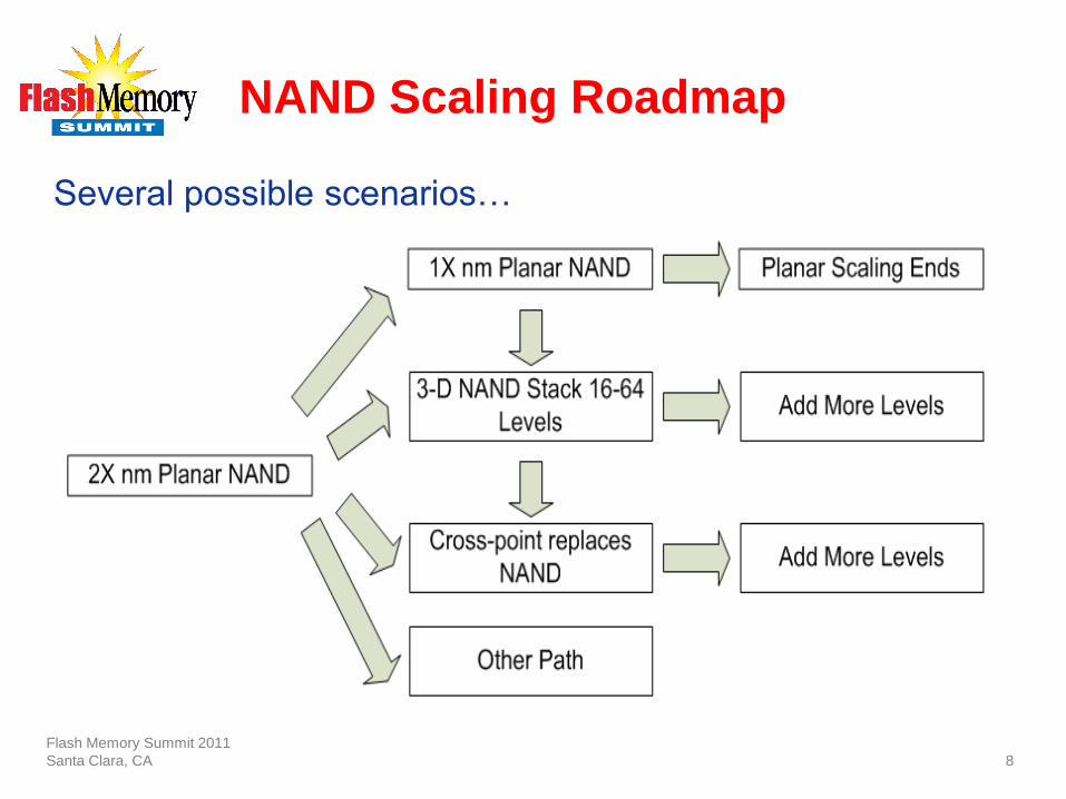
NAND Scaling Roadmap
Flash Memory Summit 2011
Santa Clara, CA 8
Several possible scenarios…
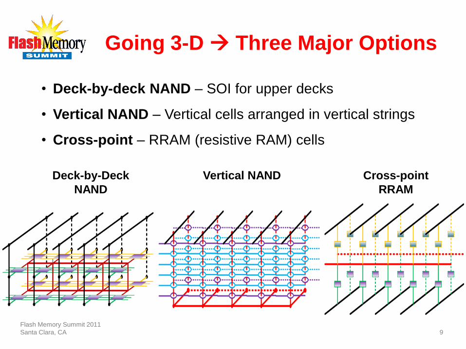
Going 3-D Three Major Options
Flash Memory Summit 2011
Santa Clara, CA 9
• Deck-by-deck NAND – SOI for upper decks
• Vertical NAND – Vertical cells arranged in vertical strings
• Cross-point – RRAM (resistive RAM) cells
Cross-point
RRAM
Deck-by-Deck
NAND
Vertical NAND
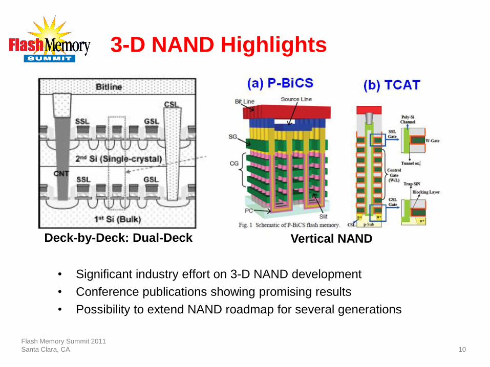
3-D NAND Highlights
Flash Memory Summit 2011
Santa Clara, CA 10
Deck-by-Deck: Dual-Deck Vertical NAND
• Significant industry effort on 3-D NAND development
• Conference publications showing promising results
• Possibility to extend NAND roadmap for several generations
Requirements for NAND Successor
• Cost structure – beat NAND costs:
MLC-capable
3-D-stackable
Simple process flow
• Scalability:
In x & y with lithography
In z with number of layers
• Reliability, performance, and power:
To meet emerging usage requirements
At component and system level
Flash Memory Summit 2011
Santa Clara, CA 11
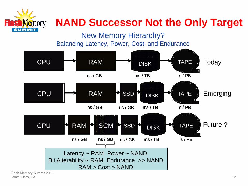
NAND Successor Not the Only TargetNew Memory Hierarchy?
Balancing Latency, Power, Cost, and Endurance
12
Flash Memory Summit 2011
Santa Clara, CA
Future ?CPU RAM DISK TAPE
ns / GB ms / TB s / PB
SSD
us / GB
PCM
ns / GB
CPUCPU RAMRAM DISKDISK TAPETAPE
ns / GB ms / TB s / PB
SSDSSD
us / GB
PCMSCM
ns / GB
TodayCPU RAM DISK TAPECPUCPU RAMRAM DISKDISK TAPETAPE
EmergingCPU RAM DISK TAPE
ns / GB ms / TB s / PB
SSD
us / GB
CPUCPU RAMRAM DISKDISK TAPETAPE
ns / GBns / GB ms / TBms / TB s / PBs / PB
SSDSSD
us / GBus / GB
ns / GB ms / TB s / PBns / GB ms / TB s / PB
Latency ~ RAM Power ~ NAND
Bit Alterability ~ RAM Endurance >> NAND
RAM > Cost > NAND
Alternative New-Memory Concepts
Explosion of ―new‖ memory concepts:
• New storage materials, new storage concepts
• Many ideas, varying functionality/cost, most unproven
13
PCM
MRAM
FERAM
CNT
Molecular
Polymer FeRAM
Word line
Polymer LayerBit line Bit line Bit line
Polymer Layer
Word line
Word line
Word line
Polymer LayerBit line Bit line Bit line
Polymer Layer
Word line
Word line
Polymer RRAMMOx-RRAM
CBRAM
Flash Memory Summit 2011
Santa Clara, CA
Phase Change Memory Case Study
• Of the emerging RRAMs, PCM is the most mature: Already in low-volume production
Demonstrated at Gb density vs. other EM at Mb density
Announced by multiple memory companies
• PCM has been heavily studied for 10+ years:Widely published – lots of good-quality technical content
Chalcogenide-based material understanding is fairly mature
Many active researchers in both industry and academia
• Provides insight into other emerging-materials systems:Many of the RRAMs share similar attributes with PCM
Flash Memory Summit 2011
Santa Clara, CA 14
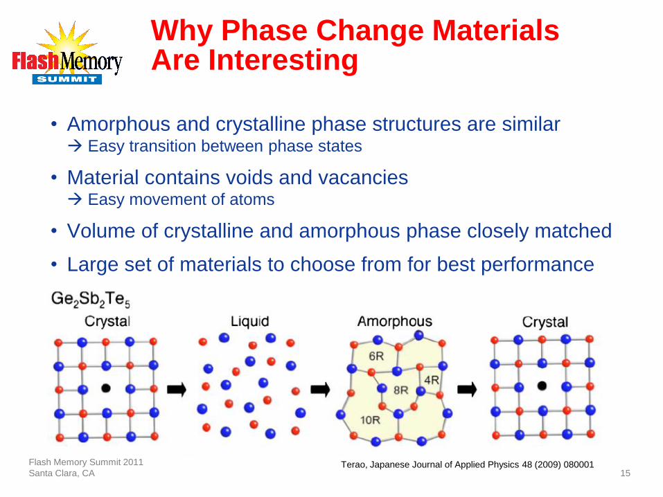
Why Phase Change MaterialsAre Interesting
• Amorphous and crystalline phase structures are similar Easy transition between phase states
• Material contains voids and vacancies Easy movement of atoms
• Volume of crystalline and amorphous phase closely matched
• Large set of materials to choose from for best performance
15Terao, Japanese Journal of Applied Physics 48 (2009) 080001Flash Memory Summit 2011
Santa Clara, CA
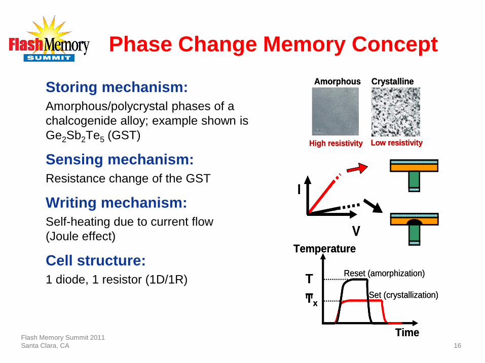
Phase Change Memory Concept
Flash Memory Summit 2011
Santa Clara, CA 16
Storing mechanism:
Amorphous/polycrystal phases of a
chalcogenide alloy; example shown is
Ge2Sb2Te5 (GST)
Sensing mechanism:
Resistance change of the GST
Writing mechanism:
Self-heating due to current flow
(Joule effect)
Cell structure:
1 diode, 1 resistor (1D/1R)
Amorphous Crystalline
High resistivity Low resistivity
Amorphous Crystalline
High resistivity Low resistivity
I
V
I
V
Time
Temperature
Tx
Tm
Reset (amorphization)
Set (crystallization)
Time
Temperature
Tx
Tm
Reset (amorphization)
Set (crystallization)
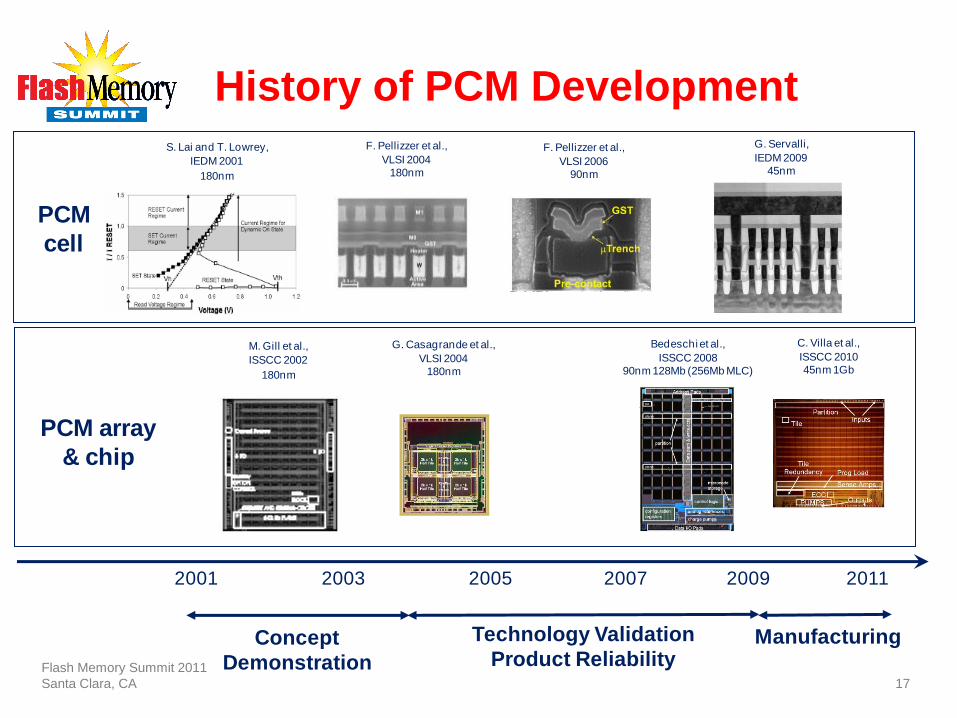
History of PCM Development
Flash Memory Summit 2011
Santa Clara, CA 17
2001 2003 2005 2007 2009 2011
M. Gill et al.,
ISSCC 2002
180nm
G. Casagrande et al.,
VLSI 2004
180nm
PCM
cell
S. Lai and T. Lowrey,
IEDM 2001
180nm
F. Pellizzer et al.,
VLSI 2006
90nm
Bedeschi et al.,
ISSCC 2008
90nm 128Mb (256Mb MLC)
G. Servalli,
IEDM 2009
45nm
PCM array
& chip
F. Pellizzer et al.,
VLSI 2004
180nm
C. Villa et al.,
ISSCC 2010
45nm 1Gb
Concept
Demonstration
Technology Validation
Product ReliabilityManufacturing
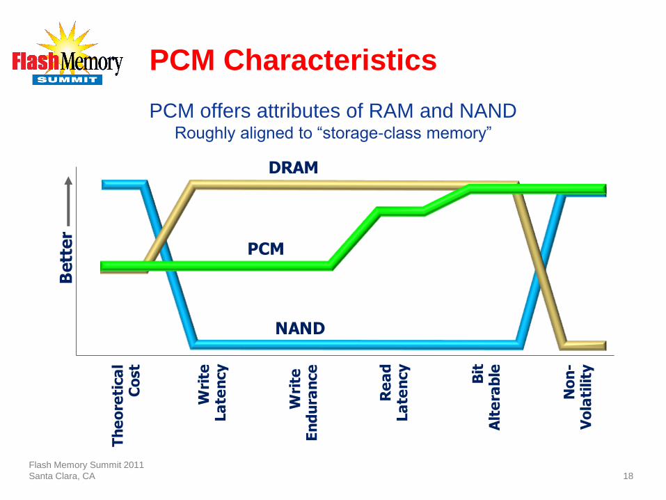
PCM Characteristics
PCM offers attributes of RAM and NANDRoughly aligned to ―storage-class memory‖
Flash Memory Summit 2011
Santa Clara, CA 18B
itA
lte
rab
le
Wri
te
En
du
ran
ce
Re
ad
La
ten
cy
Wri
teLa
ten
cy
No
n-
Vo
lati
lity
Th
eo
reti
ca
lC
ost
Bett
er
DRAM
PCM
NAND
PCM Applications Opportunities
• Wireless system to store XiP, semi-static data PCM bit alterability allows direct-write memory
• Solid state storage subsystem to store frequently accessed pages and elements that are easily managedwhen manipulated in-place PCM caching to improve performance & reliability
• Computing platforms taking advantage of nonvolatility to reduce power PCM offers endurance and write latency that are compelling for a
number of novel solutions
Flash Memory Summit 2011
Santa Clara, CA 19
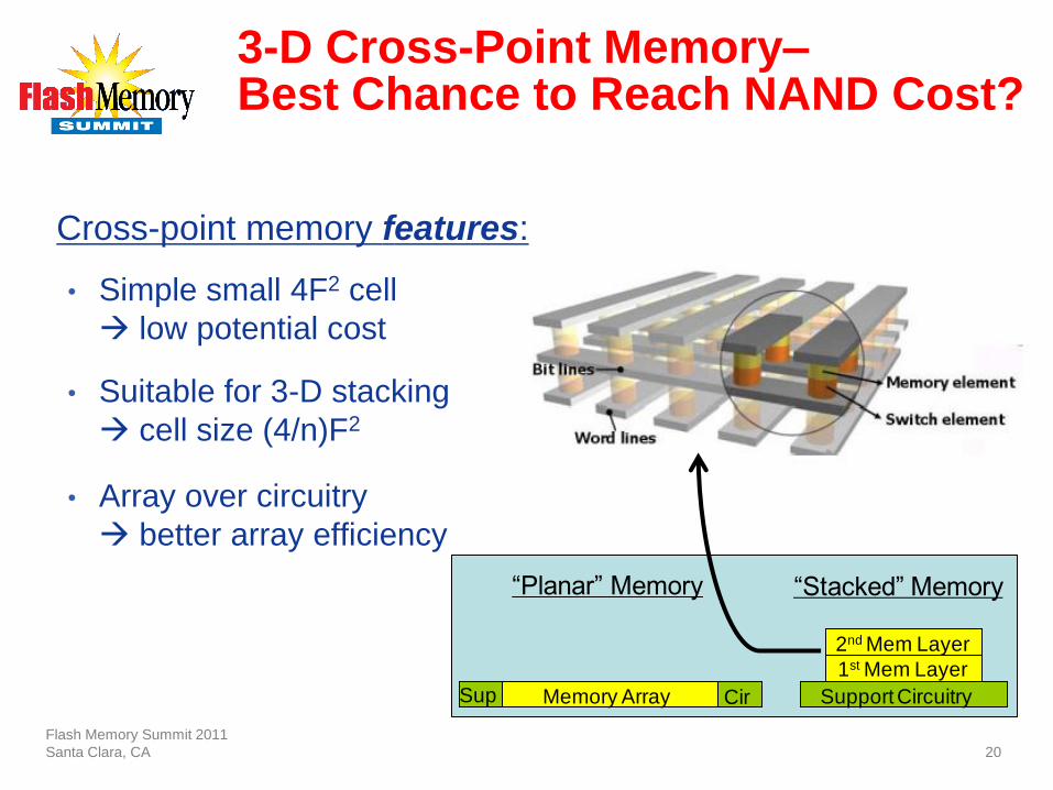
• Simple small 4F2 cell
low potential cost
• Suitable for 3-D stacking
cell size (4/n)F2
• Array over circuitry
better array efficiency
Flash Memory Summit 2011
Santa Clara, CA 20
―Planar‖ Memory ―Stacked‖ Memory
Memory Array
1st Mem Layer
2nd Mem Layer
Support CircuitrySup Cir
Cross-point memory features:
3-D Cross-Point Memory–Best Chance to Reach NAND Cost?
3-D Cross-Point Memory–Best Chance to Reach NAND Cost?
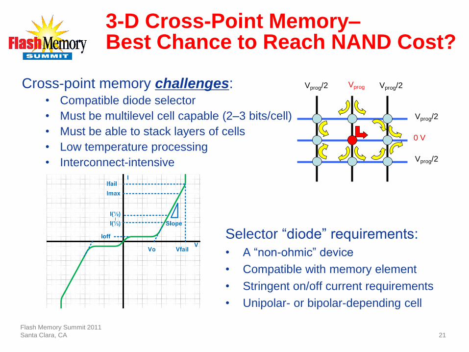
21
Cross-point memory challenges:• Compatible diode selector
• Must be multilevel cell capable (2–3 bits/cell)
• Must be able to stack layers of cells
• Low temperature processing
• Interconnect-intensive
Vprog
0 V
Vprog/2
Vprog/2
Vprog/2 Vprog/2
Selector ―diode‖ requirements:
• A ―non-ohmic‖ device
• Compatible with memory element
• Stringent on/off current requirements
• Unipolar- or bipolar-depending cell
Flash Memory Summit 2011
Santa Clara, CA
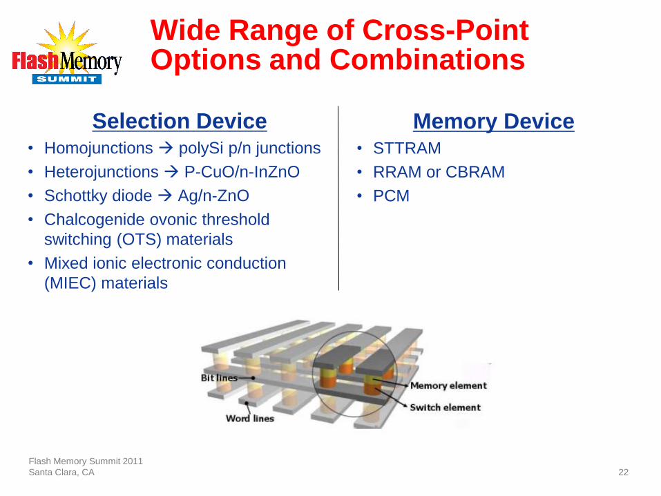
Wide Range of Cross-PointOptions and Combinations
Selection Device• Homojunctions polySi p/n junctions
• Heterojunctions P-CuO/n-InZnO
• Schottky diode Ag/n-ZnO
• Chalcogenide ovonic threshold
switching (OTS) materials
• Mixed ionic electronic conduction
(MIEC) materials
Flash Memory Summit 2011
Santa Clara, CA 22
Memory Device• STTRAM
• RRAM or CBRAM
• PCM
Phase Change-Based Cross-Point
Flash Memory Summit 2011
Santa Clara, CA 23
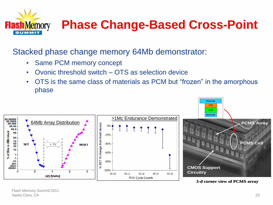
Stacked phase change memory 64Mb demonstrator:
• Same PCM memory concept
• Ovonic threshold switch – OTS as selection device
• OTS is the same class of materials as PCM but ―frozen‖ in the amorphous
phase
64Mb Array Distribution
64Mb Array Distribution
>1Mc Endurance Demonstrated>1Mc Endurance Demonstrated
CMOS Support
Circuitry
PCMS Array
3-d corner view of PCMS array
PCMS Cell
CMOS Support
Circuitry
PCMS Array
3-d corner view of PCMS array
PCMS Cell
OTS
Electrode
PCM
Electrode
OTS
Electrode
PCM
Electrode
OTS
Electrode
PCM
Electrode
Summary: A New Era Emerging for Memory!
• Increasing importance of memory to user experience:
Our lives are becoming one big shared database
• Increasing importance of memory to system performance:
Server performance and power, client portability, and instant-on
• Both NAND and DRAM facing scaling challenges:
No hard ―wall,‖ but increasing complexity
New storage concepts are emerging for cost and features
• Evolving memory hierarchy around NVM capabilities:
Moore’s Law cost treadmill NVM becoming high-performance storage
New memory features possibility of storage-class memory
Flash Memory Summit 2011
Santa Clara, CA 24
Memory is moving from a support role to a defining system role
Revisit Micron’s FMS 2011 presentations at:
www.micron.com/fms
©2011 Micron Technology, Inc. All rights reserved. Products are warranted only to meet Micron’s production data sheet specifications. Information, products,and/or
specifications are subject to change without notice. All information is provided on an ―AS IS‖ basis without warranties of any kind. Dates are estimates only.
Drawings are not to scale. Micron and the Micron logo are trademarks of Micron Technology, Inc. All other trademarks are the property of their respective owners.


![Trinity College Dublin - Memory Management Units MMUs.pdf · 2019. 11. 13. · 48bit CPU, 24bit virtual and physical address spaces, 96KB RAM, 576KB drum [disk] • OS normally attempts](https://img.pdfslide.us/doc/110x75/60c23be4b7cd7e20713772c3/trinity-college-dublin-memory-management-units-mmuspdf-2019-11-13-48bit.jpg)