Embed Size (px)
Citation preview
Conductive-bridge Memory (CBRAM®) with
Excellent High-temperature Retention and
Tolerance to High Levels of Gamma Radiation
Dr. Venkatesh P. Gopinath,
V.P. of CBRAM Technology
Adesto Technologies
Outline/Contents
• Introduction to Adesto Technologies
• Introduction to CBRAM
• CBRAM from Adesto®
– General characteristics
– High-T retention
– Radiation tolerance
• Conclusions
2

Adesto Technologies Corporate Overview
3
Overview:
Private company founded in 2007 by semiconductor industry
veterans
Locations:
Headquarters in Silicon Valley, California / Offices in Asia, Europe
Employees:
100 (Engineering=70, Sales/Marketing=20, Other=10)
Status:
$50M+ profitable business, supporting over 100 tier 1 customers
Business Model:
Discrete product manufacturing and technology licensing
Technologies:
Serial Flash / DataFlash® / CBRAM®
Solid Intellectual Property Position: Over 100 patents granted or
filed
Outline/Contents
• Introduction to Adesto Technologies
• Introduction to CBRAM
• CBRAM from Adesto
– General characteristics
– High-T retention
– Radiation tolerance
• Conclusions
4
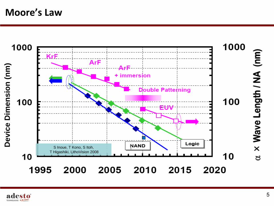
Moore’s Law
5
S Inoue, T Kono, S Itoh,
T Higashiki, LithoVision 2008
De
vic
e D
ime
ns
ion
(n
m)
6
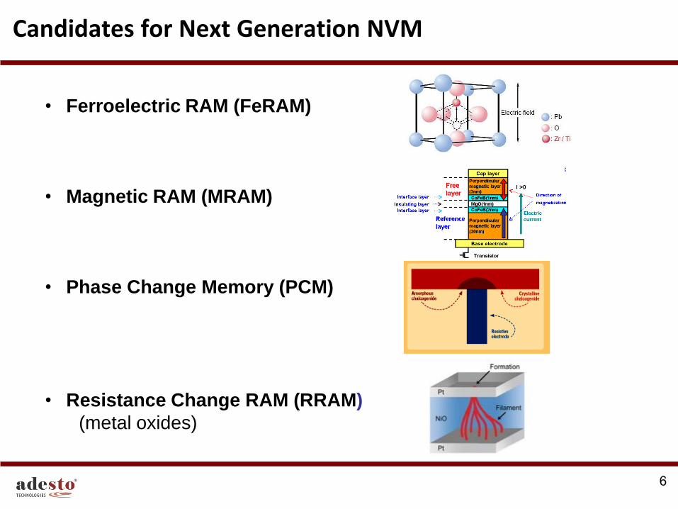
Candidates for Next Generation NVM
• Ferroelectric RAM (FeRAM)
• Magnetic RAM (MRAM)
• Phase Change Memory (PCM)
• Resistance Change RAM (RRAM)
(metal oxides)
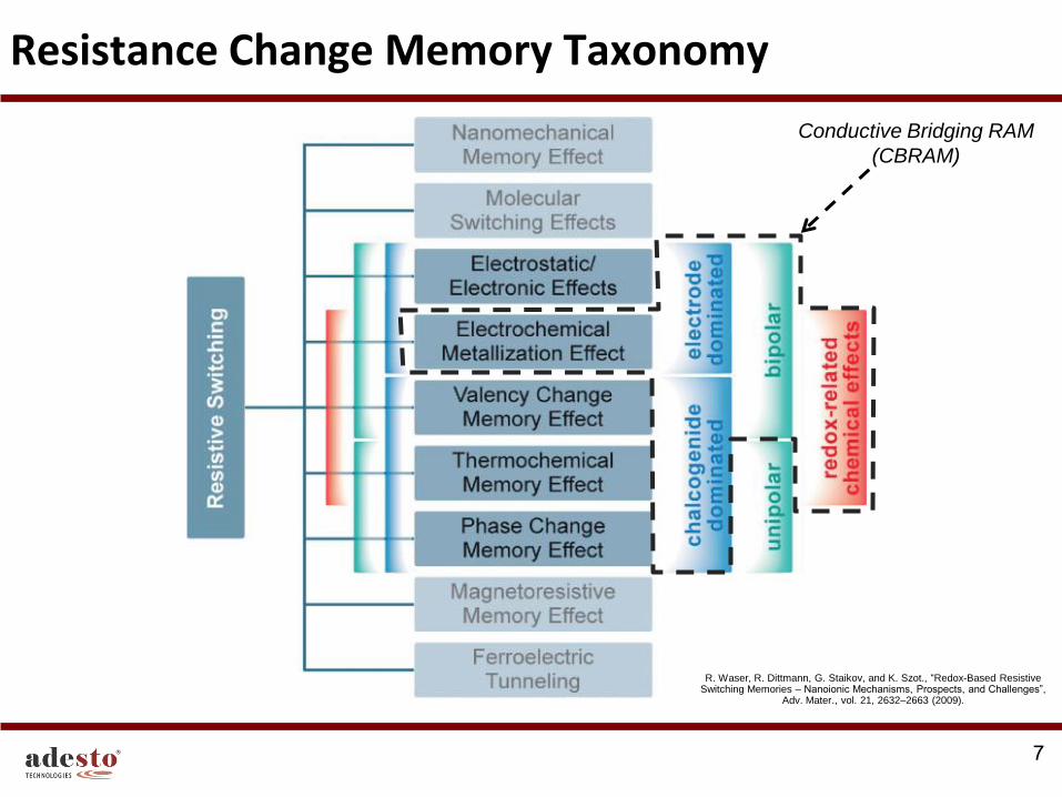
Resistance Change Memory Taxonomy
R. Waser, R. Dittmann, G. Staikov, and K. Szot., “Redox-Based Resistive Switching Memories – Nanoionic Mechanisms, Prospects, and Challenges”,
Adv. Mater., vol. 21, 2632–2663 (2009).
7
Conductive Bridging RAM
(CBRAM)
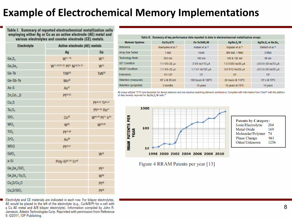
Example of Electrochemical Memory Implementations
8
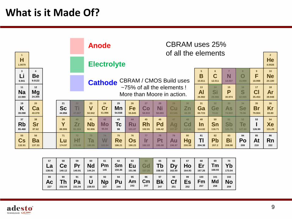
What is it Made Of?
9
53
I 126.90
52
Te 127.60
51
Sb 121.76
50
Sn 118.71
49
In 114.82
48
Cd 112.41
47
Ag 107.87
46
Pd 106.42
45
Rh 102.91
44
Ru 101.07
43
Tc 98
42
Mo 95.94
41
Nb 92.906
40
Zr 91.224
39
Y 88.906
38
Sr 87.62
37
Rb 85.468
54
Xe 131.29
85
At 210
84
Po 209
83
Bi 208.98
82
Pb 207.2
81
Tl 204.38
80
Hg 200.59
79
Au 196.97
78
Pt 195.08
77
Ir 192.22
76
Os 190.23
75
Re 186.21
74
W 183.84
73
Ta 180.95
72
Hf 178.49
71
Lu 174.97
56
Ba 137.33
55
Cs 132.91
86
Rn 222
35
Br 79.904
34
Se 78.96
33
As 74.922
32
Ge 72.61
31
Ga 69.723
30
Zn 65.39
29
Cu 63.546
28
Ni 58.693
27
Co 58.933
26
Fe 55.845
25
Mn 54.938
24
Cr 51.996
23
V 50.942
22
Ti 47.867
21
Sc 44.956
20
Ca 40.078
19
K 39.098
36
Kr 83.80
12
Mg 24.305
11
Na 22.990
17
Cl 35.453
16
S 32.065
15
P 30.974
14
Si 28.086
13
Al 26.982
18
Ar 39.948
4
Be 9.0122
3
Li 6.941
9
F 18.998
8
O 15.999
7
N 14.007
6
C 12.011
5
B 10.811
10
Ne 20.180
1
H 1.0079
2
He 4.0026
69
Tm 168.93
68
Er 167.26
67
Ho 164.93
66
Dy 162.50
65
Tb 158.93
64
Gd 157.25
63
Eu 151.96
62
Sm 150.36
61
Pm 145
60
Nd 144.24
59
Pr 140.91
58
Ce 140.12
57
La 138.91
70
Yb 173.04
101
Md 258
100
Fm 257
99
Es 252
98
Cf 251
97
Bk 247
96
Cm 247
95
Am 243
94
Pu 244
93
Np 237
92
U 238.03
91
Pa 231.04
90
Th 232.04
89
Ac 227
102
No 259
Anode
Electrolyte
Cathode
CBRAM uses 25%
of all the elements
CBRAM / CMOS Build uses
~75% of all the elements !
More than Moore in action.
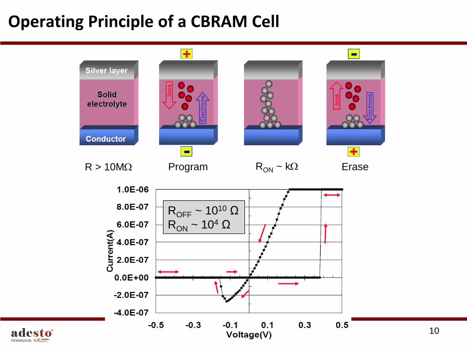
Operating Principle of a CBRAM Cell
10
Program R > 10MW RON ~ kW Erase
ROFF ~ 1010 Ω
RON ~ 104 Ω
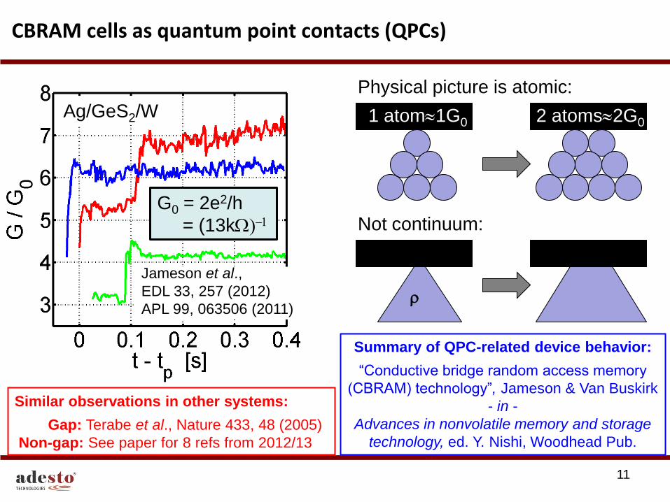
CBRAM cells as quantum point contacts (QPCs)
11
Physical picture is atomic:
Not continuum:
Ag/GeS2/W
G0 = 2e2/h
= (13kW)-1
Jameson et al.,
EDL 33, 257 (2012)
APL 99, 063506 (2011)
Similar observations in other systems:
Gap: Terabe et al., Nature 433, 48 (2005)
Non-gap: See paper for 8 refs from 2012/13
Summary of QPC-related device behavior:
“Conductive bridge random access memory
(CBRAM) technology”, Jameson & Van Buskirk
- in -
Advances in nonvolatile memory and storage
technology, ed. Y. Nishi, Woodhead Pub.
1 atom1G0 2 atoms2G0
r
Outline/Contents
• Introduction to Adesto Technologies
• Introduction to CBRAM
• CBRAM from Adesto
– General characteristics
– High-T retention
– Radiation tolerance
• Conclusions
12
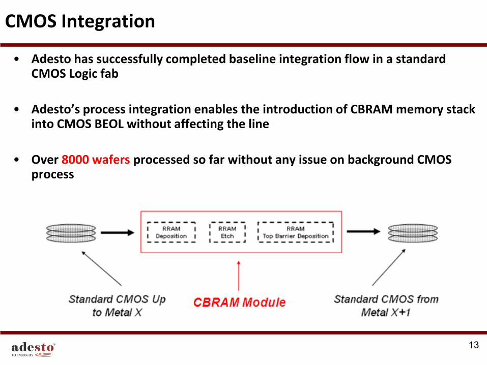
CMOS Integration
• Adesto has successfully completed baseline integration flow in a standard CMOS Logic fab
• Adesto’s process integration enables the introduction of CBRAM memory stack into CMOS BEOL without affecting the line
• Over 8000 wafers processed so far without any issue on background CMOS process
13
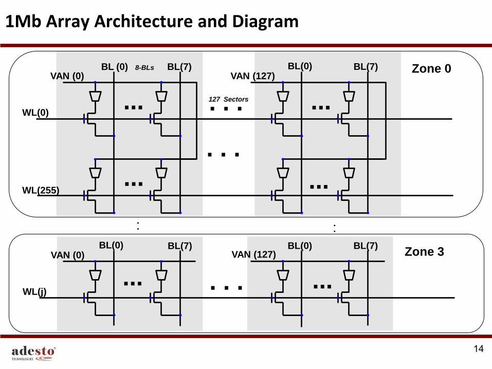
1Mb Array Architecture and Diagram
14
. . .
. . .
:
Zone 0
Zone 3
VAN (0)
WL(0)
WL(255)
VAN (127) BL (0) BL(7) BL(0) BL(7)
VAN (0)
WL(j)
BL(7) BL(0) BL(7) BL(0) VAN (127)
8-BLs
...
...
. . .
127 Sectors
:
...
...
... ...

Importance of the Fermi wavelength in QPCs
15
Metals:
lF ~ 1 Å 1 atom ~ 1 G0 (13kW)
Semiconductors:
lF >> 1 Å 1 atom << 1 G0
To reach a given
RON, a semi
QPC must be
wider than a
metal QPC
To open first conductance
channel (R~1/G0), need d~lF
Width
d
QPC Ins. Ins.
100 kW
1 MW
13/3 kW
13/2 kW
1/G0=13 kW
1 atom
3 atoms
13/N kW
RON
1 atom
N atoms
Metal Semi
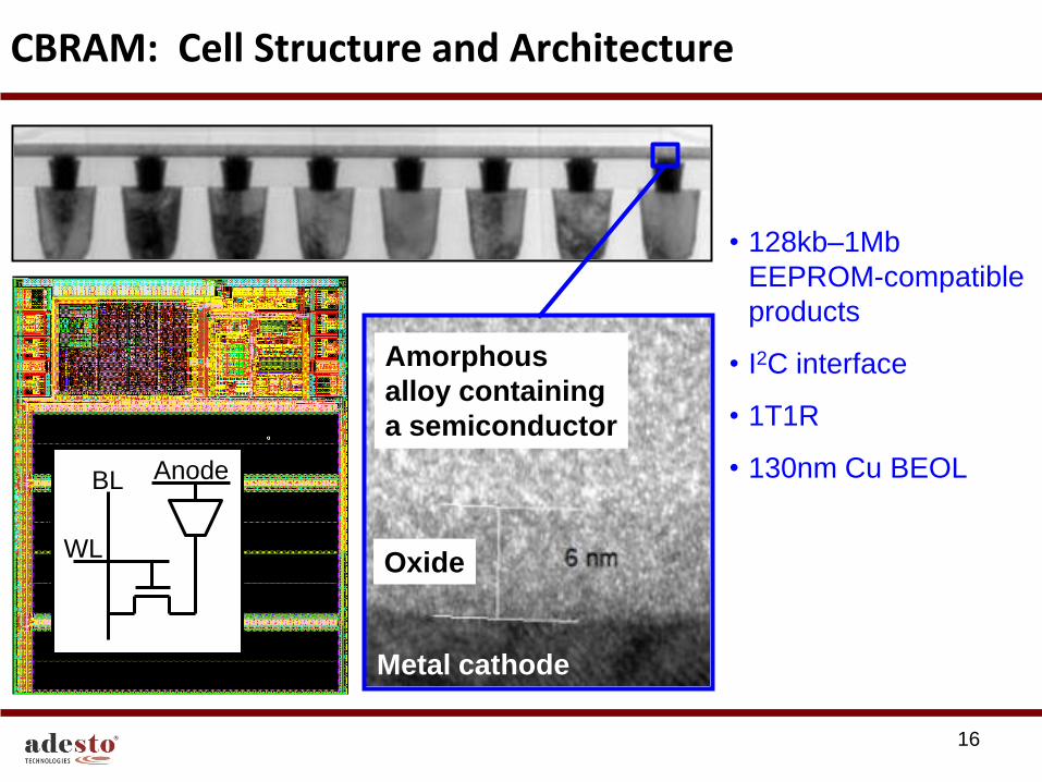
CBRAM: Cell Structure and Architecture
16
Amorphous
alloy containing
a semiconductor
Oxide
Metal cathode
BL
WL
Anode
• 128kb–1Mb
EEPROM-compatible
products
• I2C interface
• 1T1R
• 130nm Cu BEOL
Outline/Contents
• Introduction to Adesto Technologies
• Introduction to CBRAM
• CBRAM from Adesto
– General characteristics
– High-T retention
– Radiation tolerance
• Conclusions
17
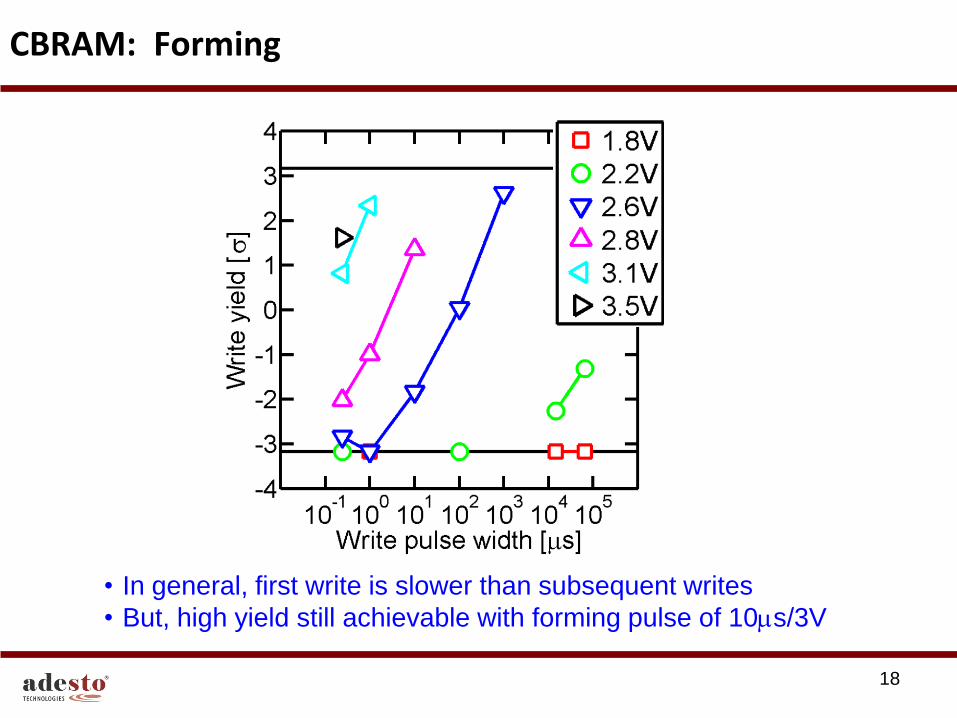
CBRAM: Forming
18
• In general, first write is slower than subsequent writes
• But, high yield still achievable with forming pulse of 10ms/3V
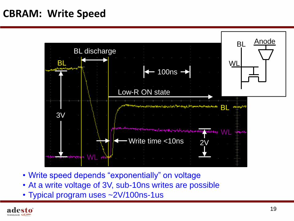
CBRAM: Write Speed
19
BL
WL
Write time <10ns
Low-R ON state
BL discharge
100ns
3V
WL
BL
2V
• Write speed depends “exponentially” on voltage
• At a write voltage of 3V, sub-10ns writes are possible
• Typical program uses ~2V/100ns-1us
BL
WL
Anode

CBRAM: Erase Speed
20
High-R OFF state Erase time ~10ns
BL
BL precharge 10ns
2V WL
BL
• Above a voltage of ~2V, sub-10ns erases are also possible
• Typical erase uses ~1.5V/100ns-1us
BL
WL
Anode
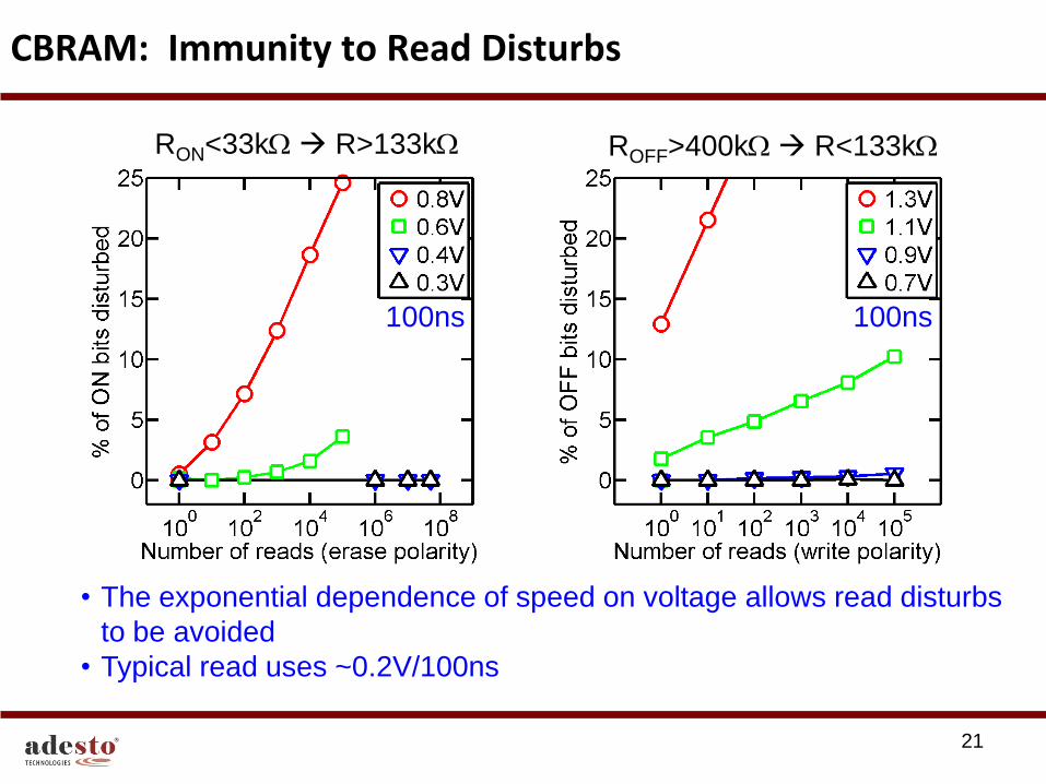
CBRAM: Immunity to Read Disturbs
21
• The exponential dependence of speed on voltage allows read disturbs
to be avoided
• Typical read uses ~0.2V/100ns
RON<33kW R>133kW ROFF>400kW R<133kW
100ns 100ns

Outline/Contents
• Introduction to Adesto Technologies
• Introduction to CBRAM
• CBRAM from Adesto
– General characteristics
– High-T retention
– Radiation tolerance
• Conclusions
22
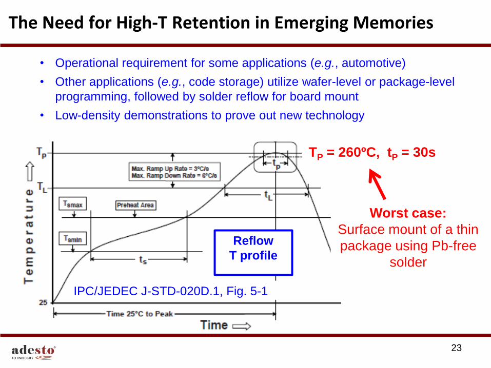
The Need for High-T Retention in Emerging Memories
23
IPC/JEDEC J-STD-020D.1, Fig. 5-1
• Operational requirement for some applications (e.g., automotive)
• Other applications (e.g., code storage) utilize wafer-level or package-level
programming, followed by solder reflow for board mount
• Low-density demonstrations to prove out new technology
TP = 260ºC, tP = 30s
Worst case:
Surface mount of a thin
package using Pb-free
solder
Reflow
T profile

CBRAM: Example of Long-term High-T Retention
24
• High-T retention of a given R state
is insensitive to the operation used
to obtain that state
~900 hours
RON = 1/G0 = 13kW
• Cells are stable at 10x greater R than
that of a 1-atom point contact of a
typical metal (i.e., ~1/G0)
• Ongoing product-level retention tests
at 110ºC have shown no fails after
more than 8 months
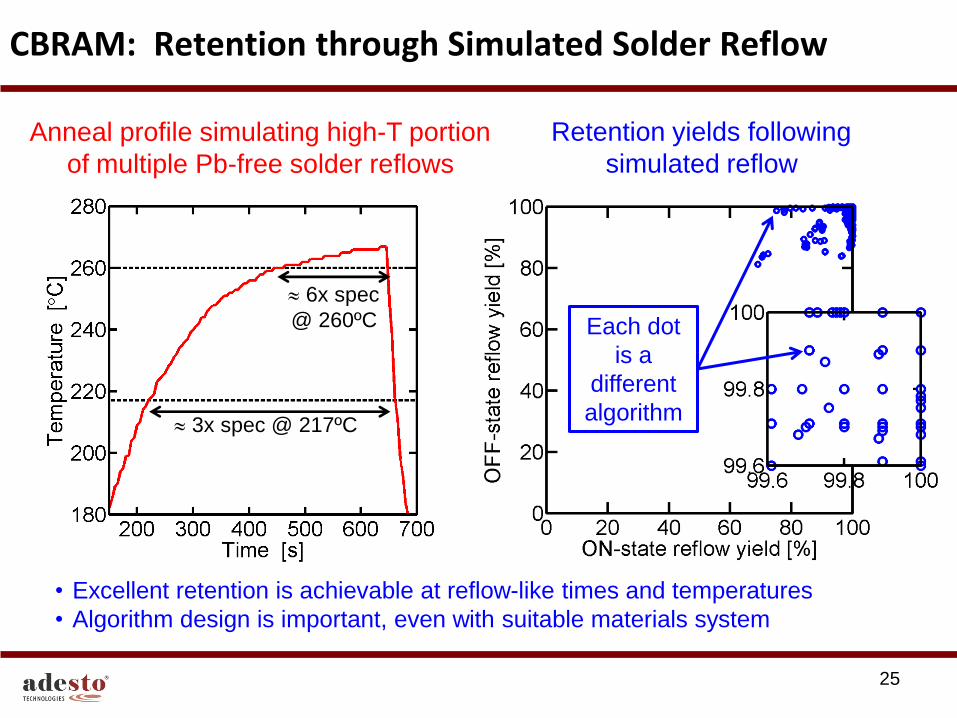
CBRAM: Retention through Simulated Solder Reflow
25
Retention yields following
simulated reflow
Each dot
is a
different
algorithm 3x spec @ 217ºC
6x spec
@ 260ºC
Anneal profile simulating high-T portion
of multiple Pb-free solder reflows
• Excellent retention is achievable at reflow-like times and temperatures
• Algorithm design is important, even with suitable materials system
Outline/Contents
• Introduction to Adesto Technologies
• Introduction to CBRAM
• CBRAM from Adesto
– General characteristics
– High-T retention
– Radiation tolerance
• Conclusions
26
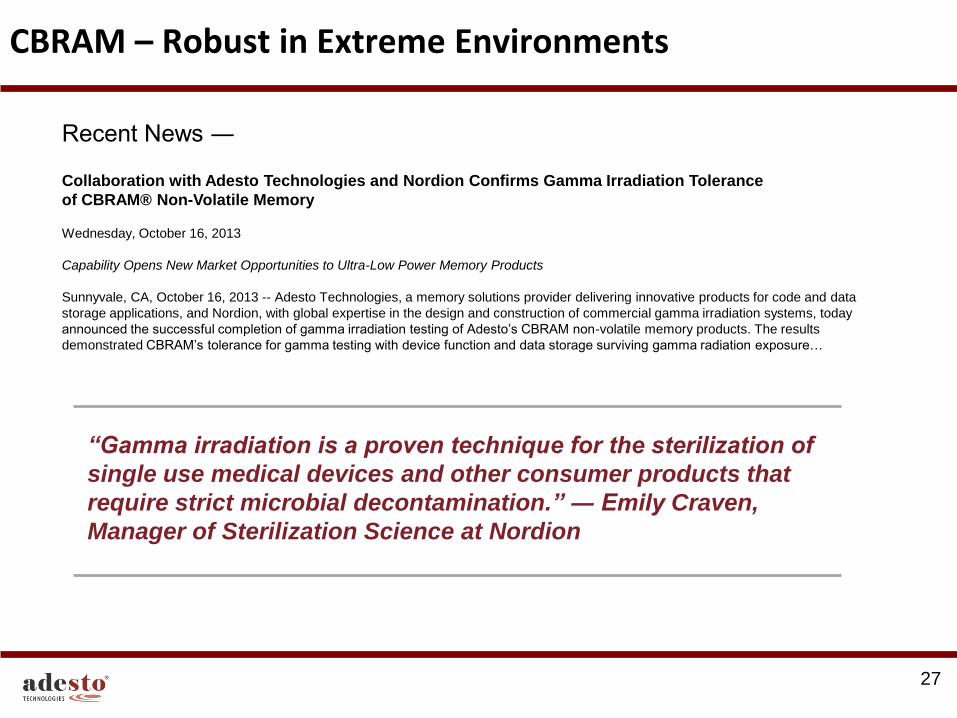
CBRAM – Robust in Extreme Environments
27
Collaboration with Adesto Technologies and Nordion Confirms Gamma Irradiation Tolerance
of CBRAM® Non-Volatile Memory
Wednesday, October 16, 2013
Capability Opens New Market Opportunities to Ultra-Low Power Memory Products
Sunnyvale, CA, October 16, 2013 -- Adesto Technologies, a memory solutions provider delivering innovative products for code and data
storage applications, and Nordion, with global expertise in the design and construction of commercial gamma irradiation systems, today
announced the successful completion of gamma irradiation testing of Adesto’s CBRAM non-volatile memory products. The results
demonstrated CBRAM’s tolerance for gamma testing with device function and data storage surviving gamma radiation exposure…
Recent News ―
“Gamma irradiation is a proven technique for the sterilization of
single use medical devices and other consumer products that
require strict microbial decontamination.” ― Emily Craven,
Manager of Sterilization Science at Nordion
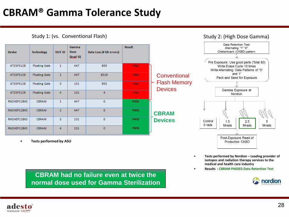
CBRAM® Gamma Tolerance Study
28
• Tests performed by Nordion – Leading provider of isotopes and radiation therapy services to the medical and health care industry
• Results : CBRAM PASSED Data Retention Test
Conventional
Flash Memory
Devices
CBRAM
Devices
CBRAM had no failure even at twice the
normal dose used for Gamma Sterilization
Study 1: (vs. Conventional Flash) Study 2: (High Dose Gamma)
• Tests performed by ASU
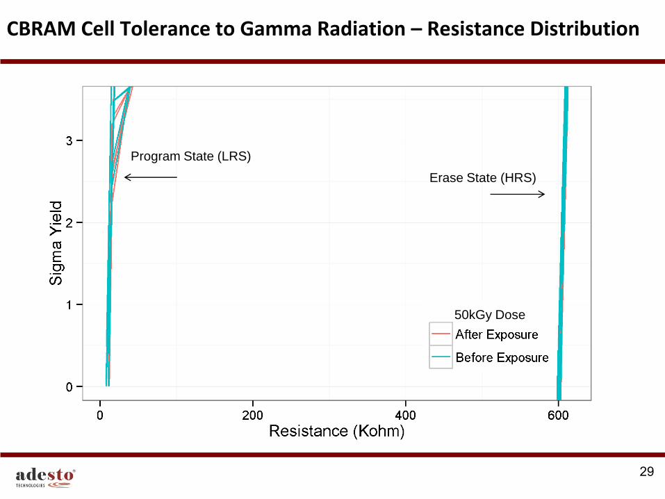
CBRAM Cell Tolerance to Gamma Radiation – Resistance Distribution
29
50kGy Dose
Program State (LRS)
Erase State (HRS)

Summary and Outlook for CBRAM
30
• Field of emerging memory is diverse and vibrant
• CBRAM has been a leading candidate, and has recently made
significant new advancements
• CBRAM has achieved high-T retention by using a combination of
materials engineering & a properly designed algorithm
Opportunities for apps w/ high-T operation or requiring solder
reflow
• Tolerance to gamma radiation has also been achieved
Opportunities for medical or aerospace applications


![Radiation Hardening by Process of CBRAM Resistance ......2020/01/06 · CBRAM, a cation based resistance switching technology [4], [8]. Additionally, recent results have demonstrated](https://img.pdfslide.us/doc/110x75/5ff833516ab95630e4480c2f/radiation-hardening-by-process-of-cbram-resistance-20200106-cbram.jpg)