Embed Size (px)
Citation preview

1
MBE grown ZnCdMgSe materials for near to mid IR wavelength
intersubband devices Joel De Jesus, Thor A. Garcia, Goupeng Chen, Vasilios Deligianakis, Arvind Ravikumar, Claire Gmachl, Aidong Shen, Maria C. Tamargo

Quantum Well
2
Barrier Barrier QW
The building block of all the intersubband devices is the Quantum Well (QW). To make a Quantum Well, a low bandgap semiconductor is sandwiched between a higher bandgap semiconductor
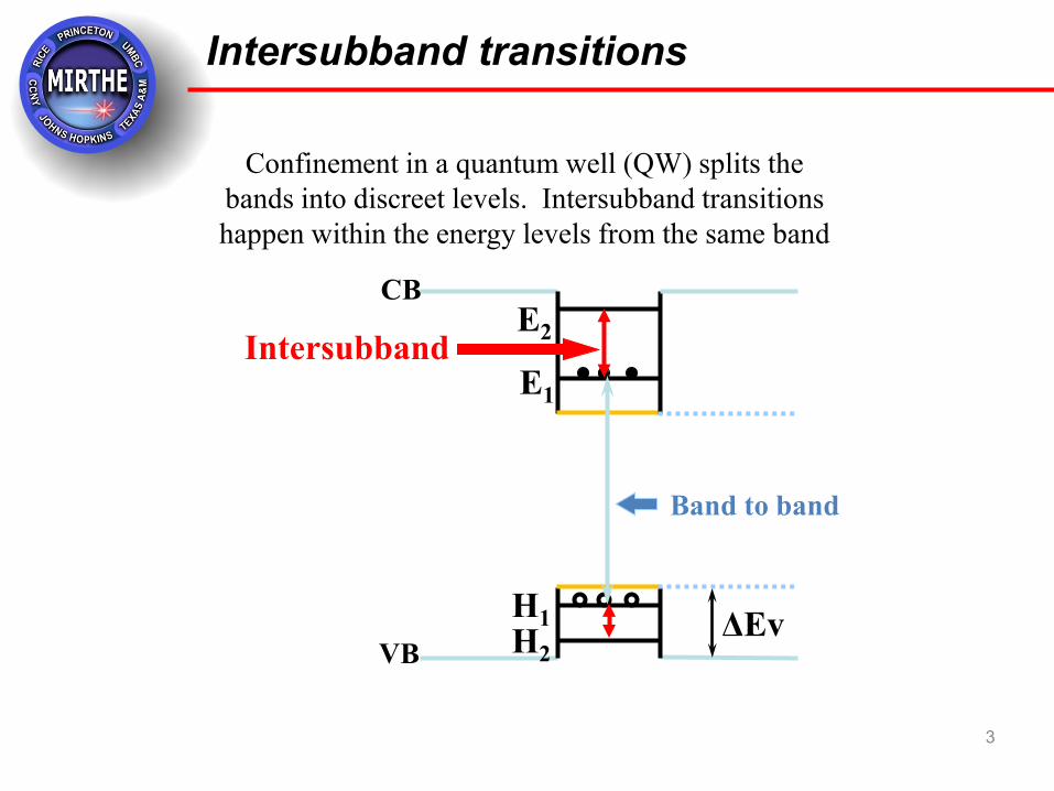
Intersubband transitions
3
H1
CB E2
E1
H2 ΔEv
VB
Band to band
Intersubband
Confinement in a quantum well (QW) splits the bands into discreet levels. Intersubband transitions happen within the energy levels from the same band

Intersubband devices
QC Laser Quantum well infrared photodetector (QWIP) Quantum Cascade
(QC) Detector
Environment Industry Medicine Military
DETECTORS EMMITERS
Quantum wells are the building blocks to make Intersubband devices
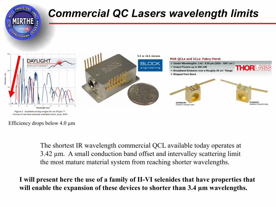
Commercial QC Lasers wavelength limits
The shortest IR wavelength commercial QCL available today operates at 3.42 µm. A small conduction band offset and intervalley scattering limit the most mature material system from reaching shorter wavelengths.
Efficiency drops below 4.0 µm
I will present here the use of a family of II-VI selenides that have properties that will enable the expansion of these devices to shorter than 3.4 µm wavelengths.
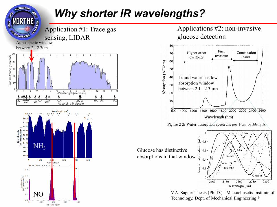
Why shorter IR wavelengths?
6
Application #1: Trace gas sensing, LIDAR
Atmospheric window between 2 - 2.7um
NH3
NO V.A. Saptari Thesis (Ph. D.) - Massachusetts Institute of Technology, Dept. of Mechanical Engineering
Applications #2: non-invasive glucose detection
Liquid water has low absorption window between 2.1 - 2.3 µm
Glucose has distinctive absorptions in that window
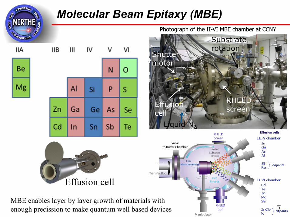
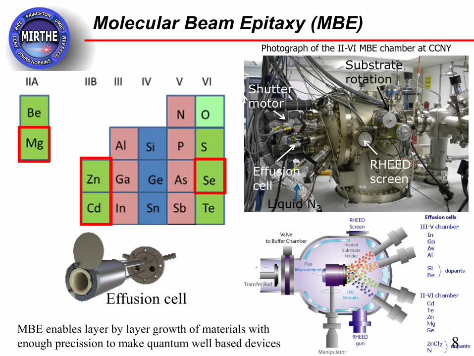
Molecular Beam Epitaxy (MBE)
7
Effusion cell
Shutter motor
Liquid N2
Substrate rotation
RHEED screen
Photograph of the II-VI MBE chamber at CCNY
7
Effusion cell
MBE enables layer by layer growth of materials with enough precission to make quantum well based devices
Molecular Beam Epitaxy (MBE)
8
Effusion cell
Shutter motor
Liquid N2
Substrate rotation
RHEED screen
Photograph of the II-VI MBE chamber at CCNY
8
Effusion cell
MBE enables layer by layer growth of materials with enough precission to make quantum well based devices

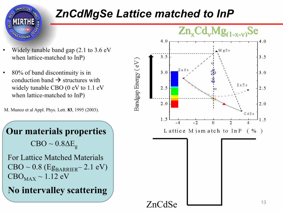
ZnCdMgSe Lattice matched to InP
9
• Widely tunable band gap (2.1 to 3.6 eV when lattice-matched to InP)
• 80% of band discontinuity is in conduction band structures with widely tunable CBO (0 eV to 1.1 eV when lattice-matched to InP)
ZnxCdyMg(1-x-y)Se
M. Munoz et al Appl. Phys. Lett. 83, 1995 (2003).
CBO ~ 0.8ΔEg
For Lattice Matched Materials CBO ~ 0.8 (EgBARRIER– 2.1 eV) CBOMAX ~ 1.12 eV
Our materials properties
No intervalley scattering
Growing lattice matched materials is like playing LEGGO

ZnCdMgSe Lattice matched to InP
10
• Widely tunable band gap (2.1 to 3.6 eV when lattice-matched to InP)
• 80% of band discontinuity is in conduction band structures with widely tunable CBO (0 eV to 1.1 eV when lattice-matched to InP)
ZnxCdyMg(1-x-y)Se
M. Munoz et al Appl. Phys. Lett. 83, 1995 (2003).
CBO ~ 0.8ΔEg
For Lattice Matched Materials CBO ~ 0.8 (EgBARRIER– 2.1 eV) CBOMAX ~ 1.12 eV
Our materials properties
No intervalley scattering ZnCdSe

ZnCdMgSe Lattice matched to InP
11
• Widely tunable band gap (2.1 to 3.6 eV when lattice-matched to InP)
• 80% of band discontinuity is in conduction band structures with widely tunable CBO (0 eV to 1.1 eV when lattice-matched to InP)
ZnxCdyMg(1-x-y)Se
M. Munoz et al Appl. Phys. Lett. 83, 1995 (2003).
CBO ~ 0.8ΔEg
For Lattice Matched Materials CBO ~ 0.8 (EgBARRIER– 2.1 eV) CBOMAX ~ 1.12 eV
Our materials properties
No intervalley scattering ZnCdSe

ZnCdMgSe Lattice matched to InP
12
• Widely tunable band gap (2.1 to 3.6 eV when lattice-matched to InP)
• 80% of band discontinuity is in conduction band structures with widely tunable CBO (0 eV to 1.1 eV when lattice-matched to InP)
ZnxCdyMg(1-x-y)Se
M. Munoz et al Appl. Phys. Lett. 83, 1995 (2003).
CBO ~ 0.8ΔEg
For Lattice Matched Materials CBO ~ 0.8 (EgBARRIER– 2.1 eV) CBOMAX ~ 1.12 eV
Our materials properties
No intervalley scattering ZnCdSe
ZnCdMgSe Lattice matched to InP
13
• Widely tunable band gap (2.1 to 3.6 eV when lattice-matched to InP)
• 80% of band discontinuity is in conduction band structures with widely tunable CBO (0 eV to 1.1 eV when lattice-matched to InP)
ZnxCdyMg(1-x-y)Se
M. Munoz et al Appl. Phys. Lett. 83, 1995 (2003).
CBO ~ 0.8ΔEg
For Lattice Matched Materials CBO ~ 0.8 (EgBARRIER– 2.1 eV) CBOMAX ~ 1.12 eV
Our materials properties
No intervalley scattering ZnCdSe

State of the art II-VI of QC Emitters
14
Long Wavelength 6.6 µm design (A3432 EL). Emits at 7.0 µm
500 1000 1500 2000 2500 30000
5
10
15
20
25
30
Wavenumbers (cm-1)
Inte
nsity
(a.u
.) 2.0 A 1.8 A 1.6 A
80 K, 80 kHz, 200 ns
500 1000 1500 2000 2500 30000
5
10
15
20
1 A
80 K 100 K 120 K 140 K 160 K 180 K 200 K 220 K 260 K 280 K
Inte
nsity
(a.u
)
Wavenumbers (cm-1)
80 kHz, 200ns1.6 A
M1_A3432_bottom
EL spectrum at High Currents Temperature dependent EL
Lorentzian peak observed
until 160 K. EL peak at 7 µm
still observed at 280 K.
59 60 61 62 63 64 65 66 67 68
B
A
BA3432 004
Small mismatch in the structure. Sharp
superlattice peaks.
XRD around InP (004)
1st Example of devices made with lattice matched materials
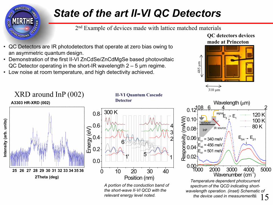
State of the art II-VI QC Detectors
15
0 10 20 30 40
0.0
0.2
0.4
0.6
0.8
6
1'
34
2
5
Ener
gy (e
V)
Position (nm)
300 K
1
1000 2000 3000 4000 50000.00
0.02
0.04
0.06
0.08
0.10
0.12
InP
epilayer
signal
IR source
E5/4 E2/1
120 K 100 K 80 K
Resp
onsiv
ity (m
A/W
)
Wavenumber (cm-1)
E3 E1
E21 = 340 meVE45 = 456 meVE41 = 501 meV
108 6 4 2Wavelength (µm)
II-VI Quantum Cascade Detector
310 µm
485
µm
• QC Detectors are IR photodetectors that operate at zero bias owing to an asymmetric quantum design.
• Demonstration of the first II-VI ZnCdSe/ZnCdMgSe based photovoltaic QC Detector operating in the short-IR wavelength 2 – 5 μm regime.
• Low noise at room temperature, and high detectivity achieved.
Temperature dependent photocurrent spectrum of the QCD indicating short-
wavelength operation. (inset) Schematic of the device used in measurements.
QC detectors devices made at Princeton
A portion of the conduction band of the short-wave II-VI QCD with the relevant energy level noted. 15
25 26 27 28 29 30 31 32 33 34 35 36
Inte
nsity
(arb
. uni
ts)
2Theta (deg)
A3303 HR-XRD (002)
XRD around InP (002)
2nd Example of devices made with lattice matched materials
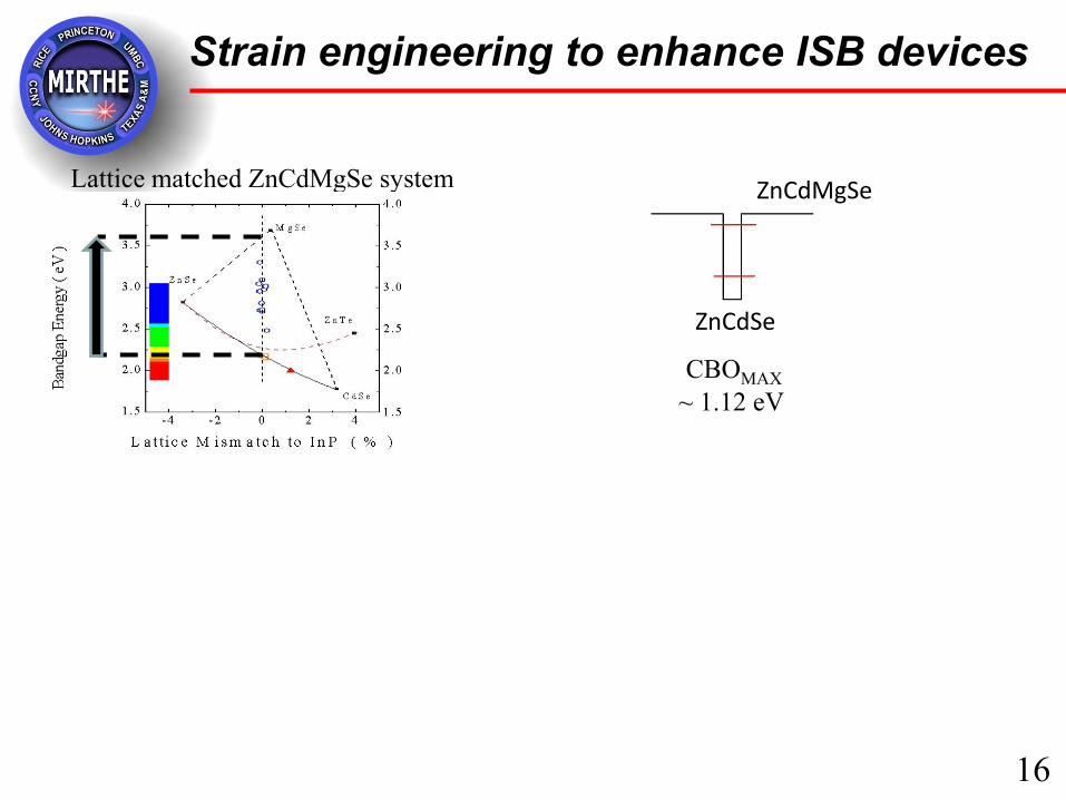
Strain engineering to enhance ISB devices
Lattice matched ZnCdMgSe system
ZnCdSe
ZnCdMgSe
CBOMAX ~ 1.12 eV
16

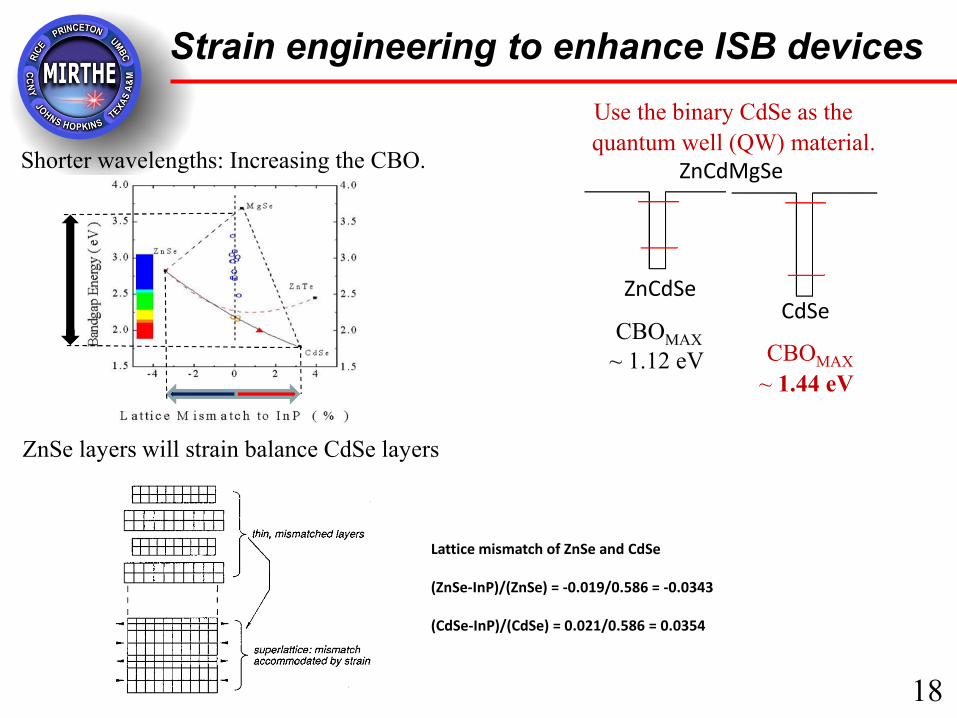
Strain engineering to enhance ISB devices
Shorter wavelengths: Increasing the CBO.
Use the binary CdSe as the quantum well (QW) material.
ZnCdSe
ZnCdMgSe
CBOMAX ~ 1.12 eV CBOMAX
~ 1.44 eV
CdSe
17
Strain engineering to enhance ISB devices
Shorter wavelengths: Increasing the CBO.
Use the binary CdSe as the quantum well (QW) material.
ZnSe layers will strain balance CdSe layers
ZnCdSe
ZnCdMgSe
CBOMAX ~ 1.12 eV CBOMAX
~ 1.44 eV
CdSe
18
Lattice mismatch of ZnSe and CdSe (ZnSe-InP)/(ZnSe) = -0.019/0.586 = -0.0343 (CdSe-InP)/(CdSe) = 0.021/0.586 = 0.0354

Strain engineering to enhance ISB devices
19
Sample tZnSe tCdSe tCdSe/tZnSe Δa/a
A 20/20 s 52 s 1.3 -0.53%
B 8/8 s 40 s 2.5 -0.41%
C 6/6 s 32 s 2.6 -0.23 %
Shorter wavelengths: Increasing the CBO.
Use the binary CdSe as the quantum well (QW) material.
ZnSe layers will strain balance CdSe layers
ZnCdSe
ZnCdMgSe
CBOMAX ~ 1.12 eV CBOMAX
~ 1.44 eV
CdSe
19

Results and discussion
A3414 A3456 A3300
XRD (004)
RT PL
FTIR Abs
500 550 600 650 700 750 800
Inte
nsity
(Arb
. uni
ts)
wavelength (nm)
1.95 eV
500 550 600 650 700 750 800
Cou
nts
Wavelength (nm)
1.86 eV
500 550 600 650 700 750 800
Inte
nsity
(Arb
. uni
ts)
wavelength (nm)
1.80 eV
56 58 60 62 64 66 68
Inte
nsity
(Arb
. Uni
ts)
2 theta56 58 60 62 64 66 68
Cou
2 Theta
2700 3000 3300 3600 3900
Energy (cm-1)
3.04 µm
2700 3000 3300 3600 3900
H
A
2.65 µm
56 58 60 62 64 66 68
Cou
nts
2 theta
B
Excellent material quality and optical properties Achieved short wavelength with only a 2.85 eV barrier energy Can extend wavelength by using higher bandgap barrier or improving QW design
Sample tCdSe RT PL FTIR Absorption
A (A3300)
52 s 1.80 eV 3.44 µm
B (A3414)
40 s 1.86 eV 3.04 µm
C (A3456)
32 s 1.95 eV 2.65 µm
All PL emissions below the bandgap of the lattice matched ZnCdSe (2.1 eV) demonstrates the achievement of deeper quantum wells.
20
2700 3000 3300 3600 3900
Arb.
Uni
ts
Energy (cm-1)
3.44 µm

Conclusions
21
• Demosntrated good electroluminescence properties from lattice matched ZnCdMgSe materials. Lasing is still elusive.
• Demonstrated good performance lattice matched ZnCdMgSe QC detectors for wavelengths as short as 2.3 µm
• Demostrated that lattice matched ZnCdMgSe systems are robust and ready for the commercialization of short to mid IR devices
• Extended the use of this material system to non-lattice matched alloys for shorter wavelengths
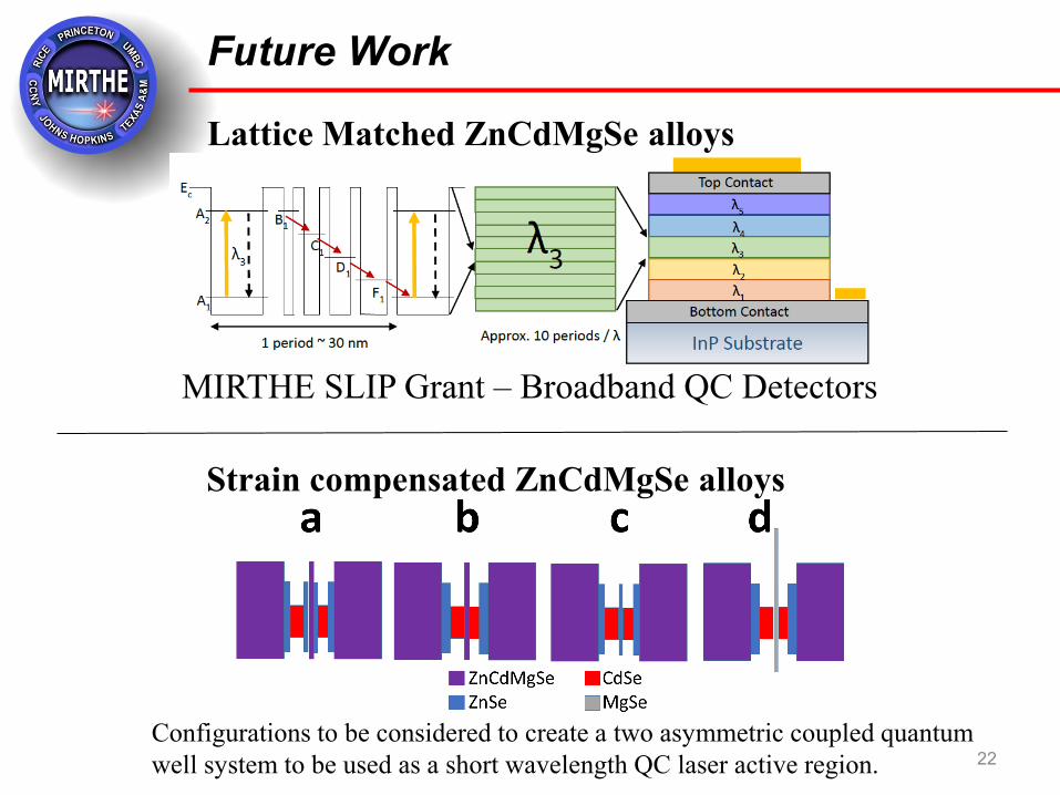
Future Work
22
Lattice Matched ZnCdMgSe alloys
Configurations to be considered to create a two asymmetric coupled quantum well system to be used as a short wavelength QC laser active region.
MIRTHE SLIP Grant – Broadband QC Detectors
Strain compensated ZnCdMgSe alloys

Special Thanks
23
Professor Maria C. Tamargo
Professor Aidong Shen
Luis Hernández Zhiyi Chen Vasilios Deligiannakis Siddharth Dhomkar
Thor Garcia Kuaile Zhao
Professor Claire Gmachl Arvind Ravikumar
Design, Processing and characterization of II-VI Devices
Guopeng Chen
Part of the collaborative
team