Embed Size (px)
Citation preview
A CRITICAL COMPARISON BETWEEN MOVPE AND MBE GROWTH OF III-V NITRIDE SEMICONDUCTOR MATERIALS FOR OPTO-ELECTRONIC
DEVICE APPLICATIONS
M.A.L. JOHNSON∗,**, ZHONGHAI YU*, J.D. BROWN*, F.A. KOECK*, N.A. EL-MASRY**,H.S. KONG***, J.A. EDMOND***, J.W. COOK, JR.*, AND J.F. SCHETZINA*
*Department of Physics, North Carolina State University, Raleigh, NC 27603 [email protected] **Department of Material Science and Engineering, North Carolina State University, Raleigh, NC 27603***Cree Research, Inc., Durham, NC
ABSTRACT
A systematic study of the growth and doping of GaN, AlGaN, and InGaN by bothmolecular beam epitaxy (MBE) and metal-organic vapor phase epitaxy (MOVPE) has beenperformed. Critical differences between the resulting epitaxy are observed in the p-type dopingusing magnesium as the acceptor species. MBE growth, using rf-plasma sources to generate theactive nitrogen species for growth, has been used for III-Nitride compounds doped either n-typewith silicon or p-type with magnesium. Blue and violet light emitting diode (LED) teststructures were fabricated. These vertical devices required a relatively high forward current andexhibited high leakage currents. This behavior was attributed to parallel shorting mechanismsalong the dislocations in MBE grown layers. For comparison, similar devices were fabricatedusing a single wafer vertical flow MOVPE reactor and ammonia as the active nitrogen species.MOVPE grown blue LEDs exhibited excellent forward device characteristics and a high reversebreakdown voltage. We feel that the excess hydrogen, which is present on the GaN surface dueto the dissociation of ammonia in MOVPE, acts to passivate the dislocations and eliminateparallel shorting for vertical device structures. These findings support the widespreadacceptance of MOVPE, rather than MBE, as the epitaxial growth technique of choice for III-Vnitride materials used in vertical transport bipolar devices for optoelectronic applications.
INTRODUCTION
The recent development of III-V Nitride semiconductor devices for optoelectronicapplications has been driven by improvements in the epitaxial growth of these semiconductormaterials. Heterostructures have been fabricated across a range of AlN-GaN-InN compositionswith bandgaps ranging from 6.2 eV (ultraviolet) to 1.9 eV (red) for LED, laser diode, andphotodetector applications [1,2]. Heterostructure epitaxy has traditionally been performed usingeither MBE or MOVPE in many semiconductor material systems [3,4]; however, most of therecent device application demonstrations for III-V nitrides have used MOVPE, particularly inthe commercially driven work at Nichia Chemical and Cree Research [5,6]. MBE growth foroptoelectronic device applications has lagged behind. Initially, this was attributed to theunavailability of an appropriate source of active nitrogen species for MBE [1]. Through thedevelopment of nitrogen rf plasma sources for MBE, the quality of the resulting epitaxial layershas improved [7,8,9,10]. Despite these advances, demonstration of high quality vertical devicessuch as laser diodes or high brightness LEDs grown by MBE has not occurred [8,11].
In this work, we compare the growth of III-V nitride materials by MBE and MOVPE inorder to examine the fundamental differences in the epitaxial growth and the influence onresulting devices. We have studied three areas of critical importance for light emitting devices.
First is the difference in the epilayer growth morphology; second is the doping of GaN withmagnesium for p-type conductivity; and finally, the deposition of InGaN quantum wells withcompositions in the visible emission range. This comparison provides a twofold benefit ofidentifying critical areas for further exploration in crystal growth and deepening theunderstanding of the underlying physical processes at work in successful epitaxial deposition.
EXPERIMENTAL PROCEDURE
MOVPE growth was performed in a vertical flow rotating wafer (up to 2000 rpm)system designed and built at NCSU. A radiatively heated substrate mount, of original highreliability design, can achieve temperatures up to 1200°C, as measured by an optical pyrometer.50-mm diameter sapphire wafers were used as the base substrate with a typical low temperatureGaN nucleation layer. Trimethylgallium (TMGa), trimethylaluminum (TMAl), trimethylindium(TMI) and ammonia were used as precursors with nitrogen and hydrogen carrier gases at areactor pressure of 76 Torr. Silane and bis(cyclopentadienyl) magnesium were used as dopantsources. Growth temperatures for GaN ranged from 1060°C to 1130°C. The conditions resultedin 2D epitaxial growth at rates of 1-2 µm/hr. InGaN growth was conducted in a manner similarto Yoshimoto at temperatures from 725°C to 800°C [12].
MBE growth was performed in an EPI Model 930 system using elemental group III anddopant sources. Rf plasma sources were used to generate the active nitrogen species. Pre-nucleated GaN/SiC substrates were used for the MBE deposition. Growth temperatures rangedfrom 750°C to 900°C for GaN and 670°C to 700°C for InGaN resulting in growth rates of 0.4-2µm/hr. A modulated beam technique was used to grow InGaN as previously described [11].
The MOVPE and MBE were connected as a multichamber UHV cluster tool. Thisallows for the growth of sophisticated heterostructures with specific layers grown in either theMBE or MOVPE system where applicable. Characterization of epitaxial layers included:scanning electron microscopy using a JEOL JSM6400 SEM, photoluminescence (PL) using a12 mW He-Cd laser source, and Nomarski microscopy using an Olympus BX60 microscopeand image capture system. Vertical cross section samples were studied in a Topcon 002BTransmission Electron Microscope (TEM) with g=(1100) at 200 kV.
LED samples were prepared following standard lithography techniques and using Ni/Auand Ti/Al as p-type and n-type contact metals, respectively.
RESULTS AND DISCUSSION
Epitaxial Layer Surface Morphology and Magnesium Doping
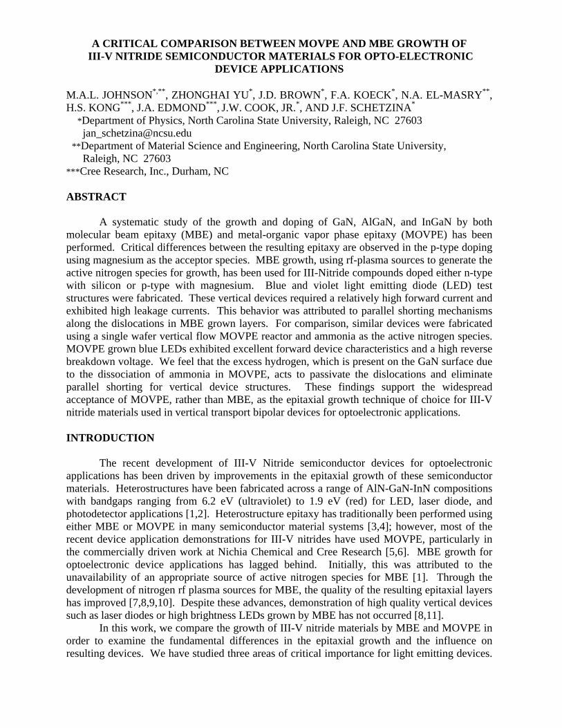
The surface morphology of epitaxially grown GaN exhibits an obvious difference betweenMOVPE and MBE deposited material. As shown in the SEM micrograph in Figure 1a,undoped or n-type doped MBE grown GaN exhibits a “wormy” structure. This surfacestructure has been previously reported and the degree of texture can be minimized, although noteliminated, through changes in the nitrogen plasma source operating conditions [8,9,10,13,14].The MOCVD grown undoped material is smooth and uniform as shown in Figure 1b.
Magnesium was used as a p-type dopant for both MBE and MOVPE grown of GaN.For MOVPE growth, the surface of p-type material is smooth and featureless. However, inMBE growth, there is a dramatic change in surface texture with the evolution of a facetedsurface with increasing magnesium flux as shown in Figures 1c and 1d. Cross sectional TEMstudies revealed the facet morphology to be related to the pre-existing dislocation structure [4].
The spacing of the contrast features in the plan view SEM image of this surface isconsistent with a dislocation density of 108-1010cm-2. We feel that this segregation is related tothe nature of doping in the MBE environment from a source that is at a lower temperature(300ºC) than the substrate (750ºC). Based on normalized flux measurements, we estimate thesticking coefficient of magnesium to be almost two orders of magnitude less than that of thegallium. As previously reported, a further increase in the magnesium flux beyond a maximumlevel results in a reduction in magnesium incorporation, a transformation in the growthmorphology observed by RHEED to 2D, and n-type conductivity behavior [16].
Hydrogen plays an important role in the p-type doping of GaN grown by MOVPE. Theformation of a Mg-H complex, with a characteristic blue PL, during subsequent activationannealing is thought to be the acceptor species responsible for p-type doping [15]. Ammoniaand carrier gasses are the source of hydrogen to the MOVPE process in a viscous flow pressureregime. Although the presence of hydrogen in the molecular flow pressure regime of MBE mayhave some influence on the surface morphology of undoped GaN layers, addition of hydrogento the nitrogen plasma does not provide a similar effect in the magnesium doping MBE grownGaN [16, 17]. A conversion in the PL spectrum to the characteristic blue has not been observedfollowing post-growth annealing of MBE deposited magnesium doped material.
Though these phenomenon are still not well understood, there is a clear differencebetween both the incorporation and activation of magnesium doped GaN grown by MOVPE ascompared with MBE. Magnesium doping by MBE results in a featured surface which wouldhave a negative impact on optoelectronic devices grown by this technique.
1 µµm 1 µµm
Figure 1: Scanning Electron Micrographs of as Grown Surfaces: a.) Undoped GaN by MBE; b.) Undoped GaN by MOVPE; c.) Magnesium Doped GaN by MBE; and d.) Magnesium Doped GaN by MOVPE.
1 µµm
a.)
1 µµm
b.)
c.) d.)
InGaN Growth
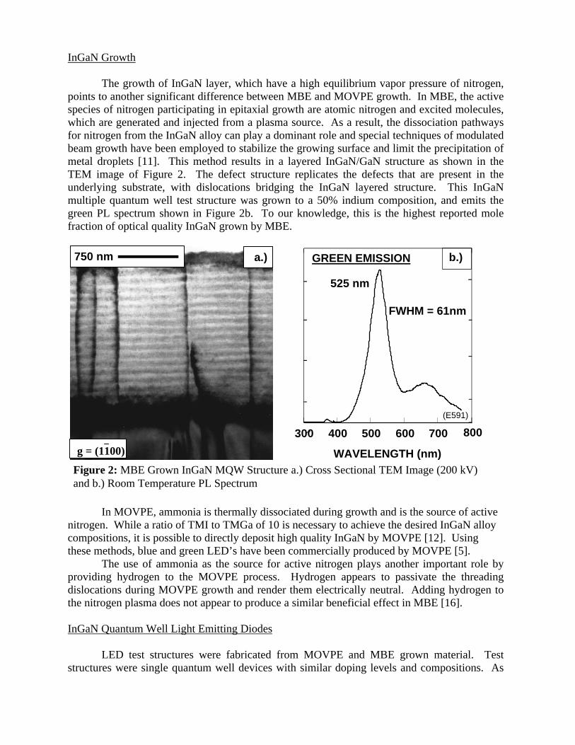
The growth of InGaN layer, which have a high equilibrium vapor pressure of nitrogen,points to another significant difference between MBE and MOVPE growth. In MBE, the activespecies of nitrogen participating in epitaxial growth are atomic nitrogen and excited molecules,which are generated and injected from a plasma source. As a result, the dissociation pathwaysfor nitrogen from the InGaN alloy can play a dominant role and special techniques of modulatedbeam growth have been employed to stabilize the growing surface and limit the precipitation ofmetal droplets [11]. This method results in a layered InGaN/GaN structure as shown in theTEM image of Figure 2. The defect structure replicates the defects that are present in theunderlying substrate, with dislocations bridging the InGaN layered structure. This InGaNmultiple quantum well test structure was grown to a 50% indium composition, and emits thegreen PL spectrum shown in Figure 2b. To our knowledge, this is the highest reported molefraction of optical quality InGaN grown by MBE.
In MOVPE, ammonia is thermally dissociated during growth and is the source of activenitrogen. While a ratio of TMI to TMGa of 10 is necessary to achieve the desired InGaN alloycompositions, it is possible to directly deposit high quality InGaN by MOVPE [12]. Usingthese methods, blue and green LED’s have been commercially produced by MOVPE [5].
The use of ammonia as the source for active nitrogen plays another important role byproviding hydrogen to the MOVPE process. Hydrogen appears to passivate the threadingdislocations during MOVPE growth and render them electrically neutral. Adding hydrogen tothe nitrogen plasma does not appear to produce a similar beneficial effect in MBE [16].
InGaN Quantum Well Light Emitting Diodes
LED test structures were fabricated from MOVPE and MBE grown material. Teststructures were single quantum well devices with similar doping levels and compositions. As
800
Figure 2: MBE Grown InGaN MQW Structure a.) Cross Sectional TEM Image (200 kV)and b.) Room Temperature PL Spectrum
700600500400300
WAVELENGTH (nm)
GREEN EMISSION
FWHM = 61nm
525 nm
(E591)
g = (1100)
b.)750 nm a.)
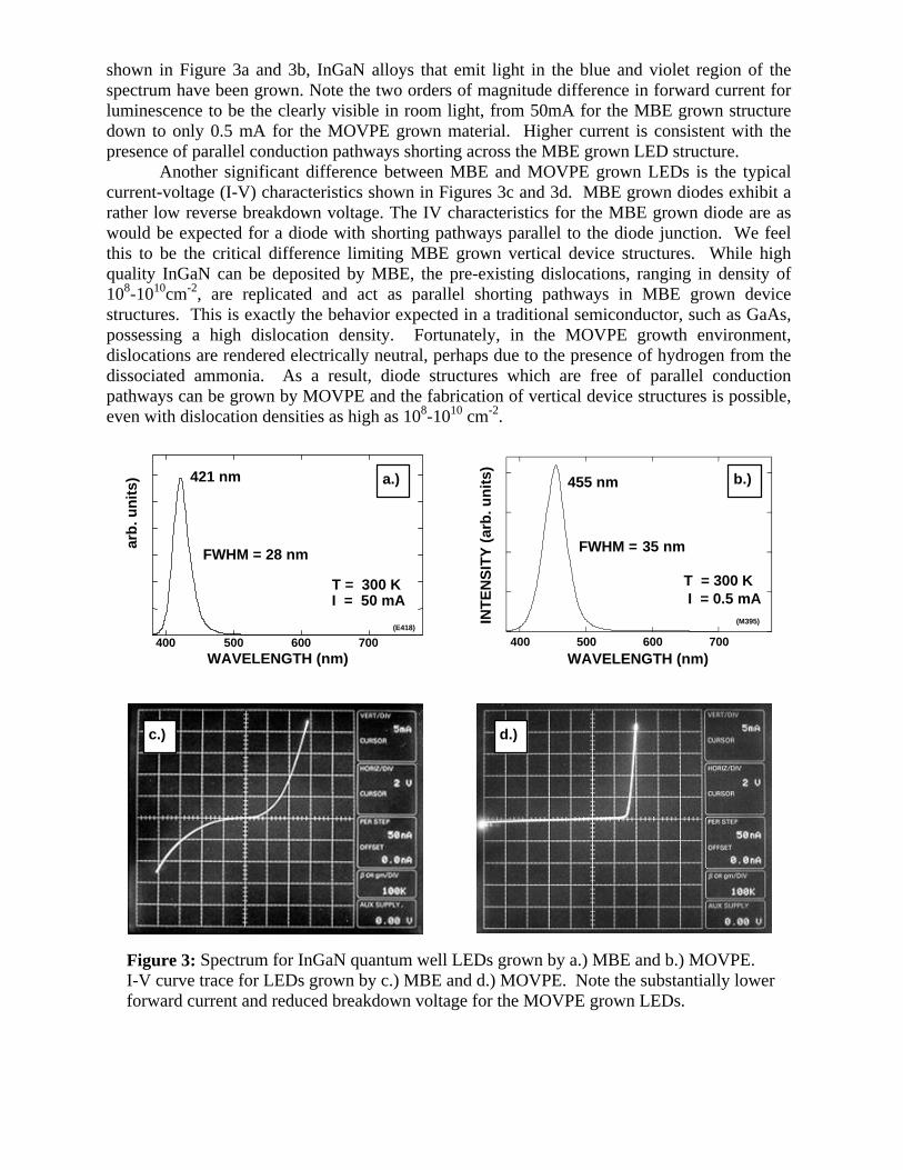
shown in Figure 3a and 3b, InGaN alloys that emit light in the blue and violet region of thespectrum have been grown. Note the two orders of magnitude difference in forward current forluminescence to be the clearly visible in room light, from 50mA for the MBE grown structuredown to only 0.5 mA for the MOVPE grown material. Higher current is consistent with thepresence of parallel conduction pathways shorting across the MBE grown LED structure.
Another significant difference between MBE and MOVPE grown LEDs is the typicalcurrent-voltage (I-V) characteristics shown in Figures 3c and 3d. MBE grown diodes exhibit arather low reverse breakdown voltage. The IV characteristics for the MBE grown diode are aswould be expected for a diode with shorting pathways parallel to the diode junction. We feelthis to be the critical difference limiting MBE grown vertical device structures. While highquality InGaN can be deposited by MBE, the pre-existing dislocations, ranging in density of108-1010cm-2, are replicated and act as parallel shorting pathways in MBE grown devicestructures. This is exactly the behavior expected in a traditional semiconductor, such as GaAs,possessing a high dislocation density. Fortunately, in the MOVPE growth environment,dislocations are rendered electrically neutral, perhaps due to the presence of hydrogen from thedissociated ammonia. As a result, diode structures which are free of parallel conductionpathways can be grown by MOVPE and the fabrication of vertical device structures is possible,even with dislocation densities as high as 108-1010 cm-2.
455 nm
FWHM = 35 nm
INT
EN
SIT
Y (
arb
. un
its)
700600500400
WAVELENGTH (nm)
T = 300 K I = 0.5 mA
(M395)
421 nm
FWHM = 28 nm
T = 300 KI = 50 mA
arb
. un
its)
700600500400WAVELENGTH (nm)
(E418)
a.)
c.)
b.)
d.)
Figure 3: Spectrum for InGaN quantum well LEDs grown by a.) MBE and b.) MOVPE.I-V curve trace for LEDs grown by c.) MBE and d.) MOVPE. Note the substantially lowerforward current and reduced breakdown voltage for the MOVPE grown LEDs.
CONCLUSIONS
We have compared the growth of III-V nitride materials by MBE and MOVPE. Criticaldifferences exist in the p-type doped GaN material. A textured surface evolves for MBE grownGaN:Mg, which may be related to the pre-existing dislocation density of the material coupledwith difficulties in depositing magnesium with its high vapor pressure at this growthtemperature. Although InGaN can be grown by either method with a bandgap tailored to emitlight in the visible range of interest for devices, the presence of a high density of shortingdislocations across the diodes limits InGaN QW LEDs grown by MBE. This is the significantfactor limiting MBE growth and allowing the successful implementation of MOVPE for III-Vnitride optoelectronic applications.
ACKNOWLEDGEMENTS
Thanks to J. Matthews for his assistance with epitaxial equipment maintenance, samplepreparation, and device processing. Financial support provided by DARPA and Cree Research.
REFERENCES
1. Strite and H. Morkoç, J. Vac. Sci. Technol. B 10, 1237 (1992). 2. S. Pearton, GaN and Related Materials, Gordon and Breach Science Publishers,
Netherlands, 1997. 3. G.B. Stringfellow, Organometallic Vapor Phase Epitaxy Theory and Practice, Academic
Press, New York, 1989. 4. M.A. Herman and H. Sitter Molecular Beam Epitaxy Fundamentals and Current Status,
Springer-Verlag, New York, 1996. 5. S. Nakamura and G. Fasol, The Blue Laser Diode Springer-Verlag, New York, 1996. 6. K. Doverspike, G.E. Bulman, S.T. Sheppard, H.S. Kong, M. Leonard, H. Dieringer, T.W.
Weeks, Jr., J. Edmond, J.D. Brown, J.T. Swindell, J.F. Schetzina, Y.K Song, M. Kuball,and A. Nurmikko, Mater. Res. Soc. Symp. Proc. 482, 1169 (1998).
7. W.C. Hughes, W. Rowland, Jr., M.A.L. Johnson, S. Fujita, J.W. Cook, Jr., J.F. Schetzina,J. Ren, and J.A. Edmond, J. Vac. Sci. Technol. B 13, 1571 (1995).
8. M.A.L. Johnson, Zhonghai Yu, C. Boney, W.H. Rowland, Jr., W.C. Hughes, J.W. Cook,Jr., and J.F. Schetzina Mater. Res. Soc. Symp. Proc. 449, 271 (1997).
9. H. Riechert, Mater. Res. Soc. Symp. Proc. 449, 149 (1997). 10. J. M. Van Hove, G.J. Cosimini, E. Nelson, A.M. Wowchak, and P.P. Chow, J. Cryst.
Growth 150, 908 (1995). 11. M.A.L. Johnson, J.D. Brown, N.A. El-Masry, J.W. Cook, Jr., J.F. Schetzina, H.S. Kong,
and J.A. Edmond J. Vac. Sci. Technol. B 16,1282 (1998). 12. N. Yoshimoto, T. Matsuoka, T. Sasaki, and A. Katsui, Appl. Phys. Lett. 59, 2251 (1991). 13. O. Zsebok, J.V. Thordson, T.G. Anderson, MRS Internet J. Nitride Semicond. Res., 3 14
(1998). 14. R.J. Molnar and T.D. Moustakis, J. Appl. Phys 76 4587 (1994). 15. J. Neugebauer and C.G. Van de Walle, Mater. Res. Soc. Symp. Proc. 395, 645 (1996). 16. M.A.L. Johnson, Zhonghai Yu, C. Boney, W.H. Rowland, Jr., W.C. Hughes, J.W. Cook,
Jr., and J.F. Schetzina Mater. Res. Soc. Symp. Proc. 449, 215 (1997). 17. S.L. Buczkowski, Zhonhai Yu, M. Richards-Babb, N.C. Giles, L.T. Romano and T.H.
Myers 449, 197 (1997).