Embed Size (px)
Citation preview
University of CaliforniaSanta Barbara (UCSB) inthe USA has been devel-
oping a hybrid technique to createIII-nitride tunnel junctions (TJs)using a combination of metal-organic chemical vapor deposition(MOCVD) and molecular beamepitaxy (MBE) [Erin C. Young etal, Appl. Phys. Express, vol9,p022102, 2016].Efficient tunnel junctions could
replace indium tin oxide (ITO)current-spreading layers with n-type gallium nitride (GaN) inlight-emitting diodes and lasers.Tunnel junctions could also be usedin multi-junction solar cells basedon III-nitride absorbing layers.Tunnel junctions are based on
flow across very thin depletionlayers in p–n junctions. Unfortu-nately, the wide bandgap of~3.4eV for GaN leads to relativelylarge 20nm depletion layers whenthe doping levels are around1x1019/cm3. Such a thick depletionlayer chokes off the tunneling cur-rent. Increasing the doping levelin GaN can be tricky, particular forp-GaN. The difficulties with p-GaNmean that device designs usuallyplace it last in the growthsequence.Most development of tunnel
junctions so far has involved MBE,but MOCVD is the preferred tech-nology in commercial production. The n-type side of the tunnel
junction was grown by ammonia(NH3) MBE on MOCVD GaN p-nand light-emitting diode deviceson free-standing semi-polar GaNsupplied by Mitsubishi Chemical.The MBE n-GaN material consisted of a thin heavily
doped layer followed by a thicker current-spreadinglayer. The optimum combination of electrical and optical characteristics – low resistance and high trans-
Technology focus: LEDs
semiconductorTODAY Compounds&AdvancedSilicon • Vol. 11 • Issue 2 • March 2016 www.semiconductor-today.com
88
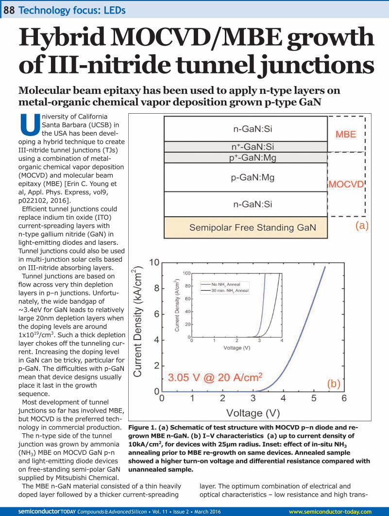
Figure 1. (a) Schematic of test structure with MOCVD p–n diode and re-grown MBE n-GaN. (b) I–V characteristics (a) up to current density of10kA/cm2, for devices with 25µm radius. Inset: effect of in-situ NH3
annealing prior to MBE re-growth on same devices. Annealed sampleshowed a higher turn-on voltage and differential resistance compared withunannealed sample.
Molecular beam epitaxy has been used to apply n-type layers on metal-organic chemical vapor deposition grown p-type GaN
Hybrid MOCVD/MBE growthof III-nitride tunnel junctions
parency — for the heavily dopedlayer was found with a carrierconcentration of ~1x10²⁰/cm3.Before MBE the samples were
cleaned in solvent. During the15-minute ramp-up to the750°C MBE re-growth tempera-ture, the top p-GaN layers wereactivated. Annealing processesfor activating p-GaN generallyremove hydrogen, which passi-vates magnesium doping. SinceNH3 was used in the MBEprocess, it was important tostart the re-growth with lowammonia flow to avoid reintro-ducing hydrogen into the p-GaNinterface. The researchers notethat the hydrogen level inammonia MBE is several ordersof magnitude lower than thatfound in MOCVD growthprocesses.The team also found that the
presence of oxygen at the inter-face could enhance performance.They comment: “The develop-ment of a controllable procedurefor introducing oxygen at thisinterface will be a key to ensuringthe repeatability of TJ devicecharacteristics.”The oxygen was detected
using atom probe tomography(APT). The researchers com-ment: “The strong overlap ofthe Mg and O suggests that adonor–acceptor complex suchas ON–2MgGa could haveformed at the interface, effec-tively preventing free surfaceMg from incorporating into then-side of the TJ during regrowth.” Such an effect could lead to a more abrupt drop-off in
magnesium concentration, improving the tunnelingthrough the depletion layer.The material was used to create devices with titanium/
gold contacts to the n-GaN material. Reference deviceswithout the tunnel junction were produced with palladium/gold p-contacts. Contacts with ITO werechromium/nickel/gold.The researchers created tunnel junction on p–n
diodes with total differential resistivity between7kA/cm2 and 10kA/cm2 of 1.5x10⁻⁴Ω-cm2, includingcontact resistance (Figure 1). The voltages at 20A/cm2
and 5kA/cm2 were 3.05V and 4.67V, respectively.
The team comments: “We consider this to be amongthe lowest resistivity and voltage characteristicsreported for any III–nitride TJ.”Comparing blue LEDs with tunnel junction and indium
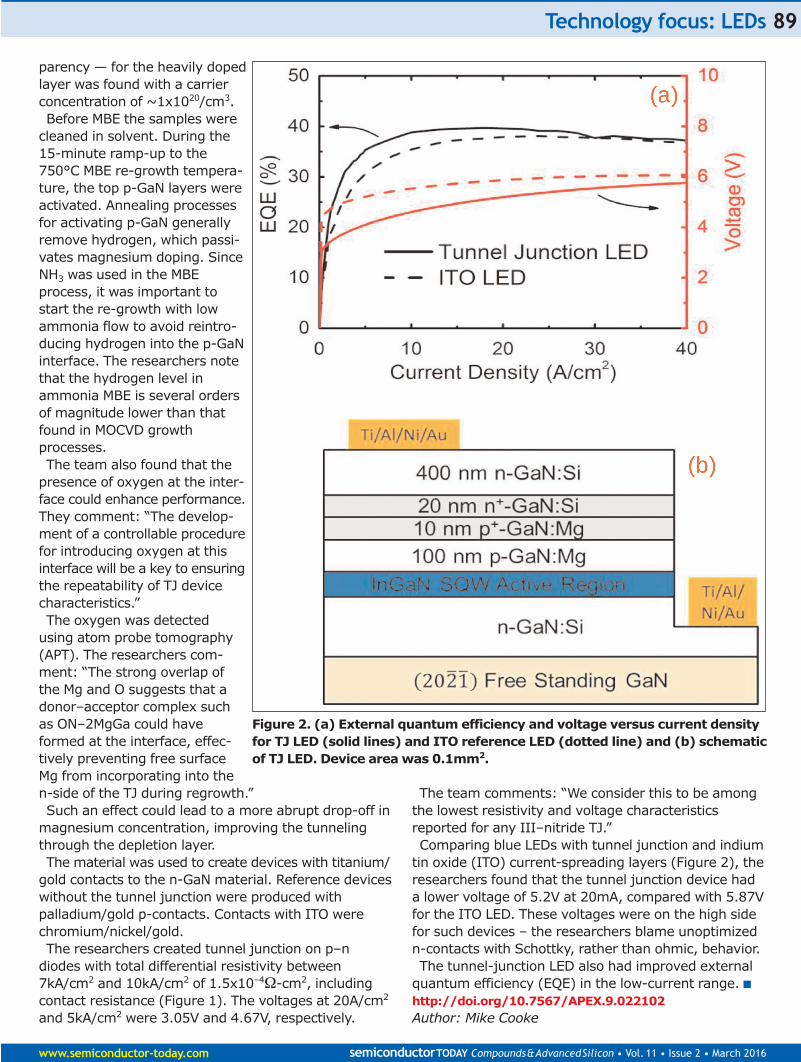
tin oxide (ITO) current-spreading layers (Figure 2), theresearchers found that the tunnel junction device hada lower voltage of 5.2V at 20mA, compared with 5.87Vfor the ITO LED. These voltages were on the high sidefor such devices – the researchers blame unoptimizedn-contacts with Schottky, rather than ohmic, behavior.The tunnel-junction LED also had improved external
quantum efficiency (EQE) in the low-current range. ■http://doi.org/10.7567/APEX.9.022102Author: Mike Cooke
Technology focus: LEDs
www.semiconductor-today.com semiconductorTODAY Compounds&AdvancedSilicon • Vol. 11 • Issue 2 • March 2016
89
Figure 2. (a) External quantum efficiency and voltage versus current densityfor TJ LED (solid lines) and ITO reference LED (dotted line) and (b) schematicof TJ LED. Device area was 0.1mm2.


![GRAfox Highlightgrafox.pdi-berlin.de/highlights/d_G_H_Faceting.pdf · for MBE[7,8] and MOCVD[12], while all other orientations resulted in faceted or macroscopically rough surfaces.[13,14,15,5]](https://img.pdfslide.us/doc/110x75/5e8806eac322fa791e09ff06/grafox-for-mbe78-and-mocvd12-while-all-other-orientations-resulted-in-faceted.jpg)