Embed Size (px)
Citation preview
www.ti.com
FEATURES
DESCRIPTION
TPS75815LOAD TRANSIENT RESPONSE
t −Time − µsTJ −Junction Temperature − C−40 −25 −10 5 20 35 50 65 80 85 110 125 0 20 40 60 80 100 120 140 160 180 200
250
200
150
100
50
0
150
100
50
0
−50
−100
−150 3
0
∆ VO
−C
hang
ein
Out
putV
olta
ge−
mV
I O−
Out
putC
urre
nt−
A
VD
O−
Dro
pout
Vol
tage
−m
V
TPS75833DROPOUT VOLTAGE
vsJUNCTION TEMPERATURE1
2345
ENIN
GNDOUTPUT
FB/NC
ENIN
GNDOUTPUT
FB/NC
12345
TO−220 (KC) PACKAGE(TOP VIEW)
TO−263 (KTT) PACKAGE(TOP VIEW)
VO = 1.5 VCO = 100 µF
IO = 3 AVO = 3.3 V
didt
0.75 A= s
TPS75801,, TPS758A01TPS75815, TPS75818TPS75825, TPS75833
SLVS330F–JUNE 2001–REVISED APRIL 2007
FAST-TRANSIENT RESPONSE, 3A, LOW-DROPOUT VOLTAGE REGULATORS
Quiescent current is 125µA at full load and drops toless than 1µA when the device is disabled. The• 3A Low-Dropout Voltage RegulatorTPS758xx is designed to have fast transient
• Available in 1.5V, 1.8V, 2.5V, and 3.3V response for large load current changes.Fixed-Output and Adjustable Versions
Because the PMOS device behaves as a low-value• Dropout Voltage Typically 150mV at 3A resistor, the dropout voltage is very low (typically(TPS75833) 150mV at an output current of 3A for the TPS75833)
• VREF and Pinout Compatible with MIC29302 and is directly proportional to the output current.Additionally, since the PMOS pass element is a(TPS758A01)voltage-driven device, the quiescent current is very• Low 125µA Typical Quiescent Currentlow and independent of output loading (typically
• Fast Transient Response 125µA over the full range of output current). These• 3% Tolerance Over Specified Conditions for two key specifications yield a significant
improvement in operating life for battery-poweredFixed-Output Versionssystems.• Available in 5-Pin TO-220 and TO-263
Surface-Mount Packages The device is enabled when EN (enable) isconnected to a high voltage level (> 2V). Applying a• Thermal Shutdown Protectionlow voltage level (< 0.7V) to EN shuts down theregulator, reducing the quiescent current to less than1µA at TJ = +25°C.
The TPS758xx family of 3A low dropout (LDO)The TPS758xx is offered in 1.5V, 1.8V, 2.5V, andregulators contains four fixed voltage option3.3V fixed-voltage versions and in an adjustableregulators and an adjustable voltage optionversion (programmable over the range of 1.22V toregulator. These devices are capable of supplying 3A5V). Output voltage tolerance is specified as aof output current with a dropout of 150mVmaximum of 3% over line, load, and temperature(TPS75833). Therefore, the device is capable ofranges. The TPS758xx family is available in a 5-pinperforming a 3.3V to 2.5V conversion.TO-220 (KC) and TO-263 (KTT) packages.
Please be aware that an important notice concerning availability, standard warranty, and use in critical applications of TexasInstruments semiconductor products and disclaimers thereto appears at the end of this data sheet.
PowerPAD is a trademark of Texas Instruments.All other trademarks are the property of their respective owners.
PRODUCTION DATA information is current as of publication date. Copyright © 2001–2007, Texas Instruments IncorporatedProducts conform to specifications per the terms of the TexasInstruments standard warranty. Production processing does notnecessarily include testing of all parameters.

www.ti.com
ABSOLUTE MAXIMUM RATINGS
DISSIPATION RATINGS TABLE
TPS75801,, TPS758A01TPS75815, TPS75818TPS75825, TPS75833SLVS330F–JUNE 2001–REVISED APRIL 2007
This integrated circuit can be damaged by ESD. Texas Instruments recommends that all integrated circuits be handled withappropriate precautions. Failure to observe proper handling and installation procedures can cause damage.
ESD damage can range from subtle performance degradation to complete device failure. Precision integrated circuits may bemore susceptible to damage because very small parametric changes could cause the device not to meet its publishedspecifications.
ORDERING INFORMATION (1)
PRODUCT VOUT
TPS758xxyyyz XX is nominal output voltage (for example, 25 = 2.5V, 01 = Adjustable).or YYY is package designator.
TPS758A01yyyz (2) Z is package quantity.
(1) For the most current specification and package information, refer to the Package Option Addendum located at the end of this datasheetor see the TI website at www.ti.com.
(2) TPS758A01 available in adjustable version only. See TPS758A01 Reference Voltage in Electrical Characteristics for different VREFrange.
Over operating junction temperature range (unless otherwise noted) (1) (2)
TPS758xx UNIT
Input voltage range, VIN –0.3 to 6 V
Voltage range at EN –0.3 to 6 V
Peak output current Internally limited
Continuous total power dissipation See Dissipation Ratings Table
Output voltage, VOUT (OUT, FB) 5.5 V
Operating junction temperature range, TJ –40 to +150 °C
Storage temperature range, TSTG –65 to +150 °C
ESD rating, HBM 2 kV
ESD rating, CDM 500 V
(1) Stresses beyond those listed under Absolute Maximum Ratings may cause permanent damage to the device. These are stress ratingsonly, and functional operation of the device at these or any other conditions beyond those indicated is not implied. Exposure toabsolute-maximum-rated conditions for extended periods may affect device reliability.
(2) All voltage values are with respect to network terminal ground.
PACKAGE RΘJC(°C/W) RΘJA(°C/W) (1)
TO-220 2 58.7 (2)
TO-263 2 38.7 (3)
(1) For both packages, the RΘJA values were computed using a JEDEC High-K board (2S2P) with a 1-ounce internal copper plane andground plane. There was no air flow across the packages.
(2) RΘJA was computed assuming a vertical, free-standing TO-220 package with pins soldered to the board. There is no heatsink attachedto the package.
(3) RΘJA was computed assuming a horizontally-mounted TO-263 package with pins soldered to the board. There is no copper padunderneath the package.
2 Submit Documentation Feedback

www.ti.com
ELECTRICAL CHARACTERISTICS
TPS75801,, TPS758A01TPS75815, TPS75818TPS75825, TPS75833
SLVS330F–JUNE 2001–REVISED APRIL 2007
Over recommended operating junction temperature range (TJ = –40°C to +125°C), VIN = VOUT(nom) + 1V, IOUT = 1mA,VEN = VIN, COUT = 100µF (unless otherwise noted). Typical values are at TJ = +25°C.
PARAMETER TEST CONDITIONS MIN TYP MAX UNIT
VIN Input voltage range (1) 2.8 5.5 V
TPS75801 1.225 VVREF Reference voltage
TPS758A01 1.24 V
Output voltage range VREF 5 V
VOUT TPS75801 VOUT + 1V ≤ VIN ≤ 5.5V, 1mA ≤ IOUT ≤ 3A –3 +3 %Accuracy (1)
TPS758A01 VOUT + 1V ≤ VIN ≤ 5.5V, 1mA ≤ IOUT ≤ 3A –3 +3 %
∆VOUT%/∆VIN Line regulation (1) VOUT + 1V ≤ VIN < 5.5V 0.04 0.1 %/V
∆VOUT%/∆IOUT Load regulation 1mA ≤ IOUT ≤ 3A 0.15 %
VDO Dropout voltage (2) VIN = 3.2V, IOUT = 3A 150 300 mV
ICL Output current limit VOUT = 0V 5.5 10 14 A
IGND Ground pin current 1mA ≤ IOUT ≤ 3A 125 200 µA
ISHDN Shutdown current (IGND) VEN = 0V 0.1 3 µA
IFB FB pin current FB = 1.5V –1 1 µA
Power-supply rejection ratioPSRR f = 100Hz, VIN = 2.8V, VOUT = 1.5V, IOUT = 3A 62 dB(ripple rejection)
VN Output noise voltage BW = 300Hz to 50kHz, VIN = 2.8V, VOUT = 1.5V 35 µVRMS
VEN(HI) Enable high (enabled) 2 V
VEN(LO) Enable low (shutdown) 0.7 V
VEN = VIN –1 1 µAIEN(HI) Enable pin current (enabled)
VEN = 0V –1 0 1 µA
Output discharge transistor current TJ = +25°C, VOUT = 1.5V 10 25 mA
Undervoltage lockout TJ = +25°C, VIN rising 2.2 2.75 VUVLO
Hysteresis VIN falling 100 mV
TSD Thermal shutdown temperature +150 °C
TJ Operating junction temperature –40 +125 °C
(1) Minimum VIN = VOUT + VDO or 2.8V, whichever is greater.(2) VIN = VOUT(nom)– 0.1V. VDO is not measured for devices with VOUT(nom) < 2.9V because minimum VIN = 2.8V.
3Submit Documentation Feedback

www.ti.com
FUNCTIONAL BLOCK DIAGRAMS
IN
GND
EN
Thermal
Shutdown
Bandgap
Reference
V = 1.22 VREF
UVLO
UVLO Current
Sense
ILIM SHUTDOWN
+-
OUT
FB
R1
R2
IN
GND
EN
Thermal
Shutdown
Bandgap
Reference
V = 1.22 VREF
UVLO
UVLO Current
Sense
ILIM SHUTDOWN
+-
OUT
R1
R2
TPS75801,, TPS758A01TPS75815, TPS75818TPS75825, TPS75833SLVS330F–JUNE 2001–REVISED APRIL 2007
ADJUSTABLE VOLTAGE VERSION
FIXED VOLTAGE VERSIONS
Table 1. TERMINAL FUNCTIONS
TPS758xx
NAME PIN NO. DESCRIPTION
EN 1 Enable input
IN 2 Input supply
GND 3 Ground
OUT 4 Regulated output voltage; see Output Capacitor section for output capacitor requirements.
FB/NC 5 Feedback voltage for adjustable device. Connect to GND or leave open for fixed VOUT devices.
4 Submit Documentation Feedback

www.ti.com
TYPICAL CHARACTERISTICS
2
IO − Output Current − A
3.330
3.270
3.315
3.285
3.2551 3
3.345
0
− O
utpu
t Vol
tage
− V
VO
VI = 4.3 VTJ = 25°C
3.3
IO − Output Current − A
1.530
1.485
1.515
1.5
1.470
1.545
0
− O
utpu
t Vol
tage
− V
VO
1.4551 32
VI = 2.8 VTJ = 25°C
TJ − Junction T emperature − °C
− O
utpu
t Vol
tage
− V
VO
3.315
5 125
3.33
3.3
20 80
3.270
3.285
3.255
3.345VI = 4.3 V
−40 −25 10 35 50 65 11095
TJ − Junction T emperature − °C
− O
utpu
t Vol
tage
− V
VO
1.470
1.485
1.530
1.5
1.455
VI = 2.8 V
1.515
1.545
−40 20 11035 95−25 −10 5 50 65 80 125
TPS75801,, TPS758A01TPS75815, TPS75818TPS75825, TPS75833
SLVS330F–JUNE 2001–REVISED APRIL 2007
TPS75833 TPS75815OUTPUT VOLTAGE OUTPUT VOLTAGE
vs vsOUTPUT CURRENT OUTPUT CURRENT
Figure 1. Figure 2.
TPS75833 TPS75815OUTPUT VOLTAGE OUTPUT VOLTAGE
vs vsJUNCTION TEMPERATURE JUNCTION TEMPERATURE
Figure 3. Figure 4.
5Submit Documentation Feedback

www.ti.com
75
100
125
150
−40 −25 −10 5 20 35 50 65 80 95 110 125
TJ − Junction T emperature − °C
Gro
und
Cur
rent
−
Aµ
VI = 5 VIO = 3 A
100k10k
PS
RR
− P
ower
Sup
ply
Rip
ple
Rej
ectio
n −
dB
f − Frequency − Hz
70
60
50
40
30
20
10
0
90
80
1k10010 1M
IO = 1 mA
IO = 3 A
10M
VI = 4.3 VCo = 100 µFTJ = 25°C
0
0.5
1
1.5
2
2.5
IO = 3 A
IO = 1 mA
f − Frequency − Hz1010 100 1k 10k 100k
VI = 4.3 VVO = 3.3 VCo = 100 µFTJ = 25°C
V/
Hz
Out
put S
pect
ral N
oise
Den
sity
−
µ
f − Frequency − Hz
− O
utpu
t Im
peda
nce
−z
oΩ
10 100 100k 1M
0.001
10k1k 10M
1
100
IO = 1 mA
0.01
0.1
10
IO = 3 A
0.0001
0.00001
VI = 4.3 VCo = 100 µFIO = 1 mATJ = 25°C
TPS75801,, TPS758A01TPS75815, TPS75818TPS75825, TPS75833SLVS330F–JUNE 2001–REVISED APRIL 2007
TYPICAL CHARACTERISTICS (continued)
TPS758xx TPS75833GROUND CURRENT POWER-SUPPLY RIPPLE REJECTION
vs vsJUNCTION TEMPERATURE FREQUENCY
Figure 5. Figure 6.
TPS75833 TPS75833OUTPUT SPECTRAL NOISE DENSITY OUTPUT IMPEDANCE
vs vsFREQUENCY FREQUENCY
Figure 7. Figure 8.
6 Submit Documentation Feedback

www.ti.com
0
50
100
150
200
250
−40 −25 −10 5 20 35 50 65 80 95 110 125TJ − Junction T emperature − °C
− D
ropo
ut V
olta
ge −
mV
VD
O
VO= 3.3 VIO = 3 A
0
50
100
150
200
250
2.5 3 3.5 4 4.5 5VI − Input V oltage − V
− D
ropo
ut V
olta
ge −
mV
VD
O
IO = 3 A
TJ = 25°C
TJ = −40°C
TJ = 125°C
3.8
0
−50
VI
t − Time − µs0 15010050 200 250 350300 400 450 500
− In
put V
olta
ge −
V
VO = 1.5 VIO = 3 ACo = 100 µF
2.8
−100
50
∆VO
− C
hang
e in
Out
put V
olta
ge −
mV
2
3
4
1.5 2.5 3.52 3
− M
inim
um R
equi
red
Inpu
t Vol
tage
− V
VO − Output V oltage − V
VI
2.8
1.75 2.25 2.75 3.25
IO = 3 A
TJ = 125°C
TJ = 25°C
TJ = −40°C
TPS75801,, TPS758A01TPS75815, TPS75818TPS75825, TPS75833
SLVS330F–JUNE 2001–REVISED APRIL 2007
TYPICAL CHARACTERISTICS (continued)
TPS75801 TPS75833DROPOUT VOLTAGE DROPOUT VOLTAGE
vs vsINPUT VOLTAGE JUNCTION TEMPERATURE
Figure 9. Figure 10.
MINIMUM REQUIRED INPUT VOLTAGEvs TPS75815
OUTPUT VOLTAGE LINE TRANSIENT RESPONSE
Figure 11. Figure 12.
7Submit Documentation Feedback

www.ti.com
t − Time − µs
VI
− In
put V
olta
ge −
V
15010050 200 250 350300 400 450 5000
−100
5.3
0
4.3
VO = 3.3 VIO = 3 ACo = 100 µF
50
−50
100
∆VO
− C
hang
e in
Out
put V
olta
ge −
mV
t − Time − µs
−100
0
0 604020 80 100 140120 160 180 200
0
50
−50
VO = 1.5 VCo = 100 µF
−150 3
didt
0.75 As
I −
Out
put C
urre
nt −
A
O
VO
∆−
Cha
nge
in O
utpu
t Vol
tage
− m
V
100
150
t − Time − µs
I −
Out
put C
urre
nt −
A
O
4
604020 80 100 140120 160 180 2000
100
200
0
VO = 3.3 VCo = 100 µF
−100
2
0
didt
0.75 As
VO
∆−
Cha
nge
in O
utpu
t Vol
tage
− m
V
t − Time (Start-Up) − ms0
3.3
0
0
4.3
0.2 10.4 0.6 0.8
− O
utpu
t Vol
tage
− V
VO
Ena
ble
Vol
tage
− V
VI = 4.3 VIO = 10 mATJ = 25°C
TPS75801,, TPS758A01TPS75815, TPS75818TPS75825, TPS75833SLVS330F–JUNE 2001–REVISED APRIL 2007
TYPICAL CHARACTERISTICS (continued)
TPS75815 TPS75833LOAD TRANSIENT RESPONSE LINE TRANSIENT RESPONSE
Figure 13. Figure 14.
TPS75833TPS75833 OUTPUT VOLTAGE AND ENABLE VOLTAGE
LOAD TRANSIENT RESPONSE TIME (START-UP)
Figure 15. Figure 16.
8 Submit Documentation Feedback
www.ti.com
IN
EN
OUT
+
GND
Co
ESR
RL
VITo Load
0.010 3
10
IO − Output Current − A
ES
R −
Equ
ival
ent S
erie
s R
esis
tanc
e −
Ω
1
0.1
0.015
Co = 680 µFTJ = 25°C
1 2
Region of Stability
Region of Instability0.01
0 3
10
IO − Output Current − A
1
0.2
ES
R −
Equ
ival
ent S
erie
s R
esis
tanc
e −
Ω
Co = 47 µFTJ = 25°C
1 2
Region of Stability
Region of Instability
TPS75801,, TPS758A01TPS75815, TPS75818TPS75825, TPS75833
SLVS330F–JUNE 2001–REVISED APRIL 2007
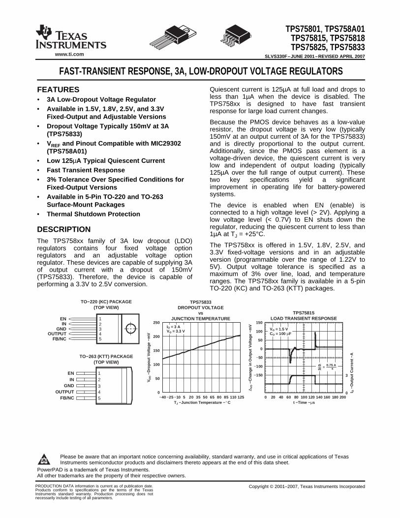
Figure 17. Test Circuit for Typical Regions of Stability (Figure 18 and Figure 19) (Fixed Output Options)
TYPICAL REGION OF STABILITY TYPICAL REGION OF STABILITYEQUIVALENT SERIES RESISTANCE(A) EQUIVALENT SERIES RESISTANCE(A)
vs vsOUTPUT CURRENT OUTPUT CURRENT
Figure 18. Figure 19.
A. Equivalent series resistance (ESR) refers to the total series resistance, including the ESR of the capacitor,any series resistance added externally, and printed wiring board (PWB) trace resistance to COUT.
9Submit Documentation Feedback

www.ti.com
DETAILED DESCRIPTION
Pin Functions
Enable (EN)
Feedback (FB)
Input Voltage (IN)
Output Voltage (OUTPUT)
APPLICATION INFORMATION
Programming the TPS75801 Adjustable LDO Regulator
VO VREF 1R1R2
(1)
R1 VO
VREF1 R2
(2)
TPS75801,, TPS758A01TPS75815, TPS75818TPS75825, TPS75833SLVS330F–JUNE 2001–REVISED APRIL 2007
The TPS758xx family includes four fixed-output voltage regulators (1.5V, 1.8V, 2.5V, and 3.3V), and anadjustable regulator, the TPS75801 (adjustable from 1.22V to 5V). The bandgap voltage is typically 1.22V.
The EN terminal is an input which enables or shuts down the device. If EN is a low voltage level (< 0.7V), thedevice will be in shutdown or sleep mode. When EN goes to a high voltage level (> 2V), the device will beenabled.
FB is an input terminal used for the adjustable-output option and must be connected to the output terminal eitherdirectly, in order to generate the minimum output voltage of 1.22V, or through an external feedback resistordivider for other output voltages. The FB connection should be as short as possible. It is essential to route theterminal so that it minimizes/avoids noise pickup. Adding RC networks between the FB terminal and VOUT tofilter noise is not recommended because it may cause the regulator to oscillate.
The VIN terminal is an input to the regulator.
The VOUTPUT terminal is an output from the regulator.
The output voltage of the TPS75801 adjustable regulator is programmed using an external resistor divider asshown in Figure 20. The output voltage is calculated using:
Where:VREF = 1.224V typ (the internal reference voltage).
Resistors R1 and R2 should be chosen for approximately 40µA divider current. Lower value resistors can beused but offer no inherent advantage and waste more power. Higher values should be avoided as leakagecurrents at FB increase the output voltage error. The recommended design procedure is to choose R2 = 30.1kΩto set the divider current at 40µA and then calculate R1 using:
10 Submit Documentation Feedback

www.ti.com
VO
VI
OUT
FB
R1
R2GND
EN
IN
≤ 0.7 V≥ 2 V
TPS75801
1 µF
Co
OUTPUT VOLTAGEPROGRAMMING GUIDE
OUTPUTVOLTAGE
R1 R2
2.5 V
3.3 V
3.6 V
UNIT
31.6
51
58.3
30.1
30.1
30.1
kΩkΩkΩ
Regulator Protection
Input Capacitor
Output Capacitor
TPS75801,, TPS758A01TPS75815, TPS75818TPS75825, TPS75833
SLVS330F–JUNE 2001–REVISED APRIL 2007
APPLICATION INFORMATION (continued)
Figure 20. TPS75801 Adjustable LDO Regulator Programming
The TPS758xx PMOS-pass transistor has a built-in back diode that conducts reverse currents when the inputvoltage drops below the output voltage (for example, during power down). Current is conducted from the outputto the input and is not internally limited. When extended reverse voltage is anticipated, external limiting may beappropriate.
The TPS758xx also features internal current limiting and thermal protection. During normal operation, theTPS758xx limits output current to approximately 10A. When current limiting engages, the output voltage scalesback linearly until the overcurrent condition ends. While current limiting is designed to prevent gross devicefailure, care should be taken not to exceed the power dissipation ratings of the package. If the temperature ofthe device exceeds –150°C (typ), thermal-protection circuitry shuts it down. Once the device has cooled below+130°C (typ), regulator operation resumes.
For a typical application, a ceramic input bypass capacitor (0.22µF to 1µF) is recommended to ensure devicestability. This capacitor should be as close as possible to the input pin. Due to the impedance of the inputsupply, large transient currents will cause the input voltage to droop. If this droop causes the input voltage todrop below the UVLO threshold, the device will turn off. Therefore, it is recommended that a larger capacitor beplaced in parallel with the ceramic bypass capacitor at the regulator input. The size of this capacitor depends onthe output current, response time of the main power supply, and the distance of the main power supply to theregulator. At a minimum, the capacitor should be sized to ensure that the input voltage does not drop below theminimum UVLO threshold voltage during normal operating conditions.
As with most LDO regulators, the TPS758xx requires an output capacitor connected between OUT and GND tostabilize the internal control loop. The minimum recommended capacitance value is 47µF with an ESR(equivalent series resistance) of at least 200mΩ. As shown in Figure 21, most capacitor and ESR combinationswith a product of 47–6 x 0.2 = 9.4–6 or larger will be stable, provided the capacitor value is at least 47µF. Solidtantalum electrolytic and aluminum electrolytic capacitors are all suitable, provided they meet the requirementsdescribed in this section. Larger capacitors provide a wider range of stability and better load transient response.
This information and the ESR graphs shown in Figure 18, Figure 19, and Figure 21, is included to assist inselection of suitable capacitance for the user's application. When necessary to achieve low height requirementswith high output current and/or high load capacitance, several higher ESR capacitors can be used in parallel tomeet these guidelines.
11Submit Documentation Feedback

www.ti.com
100
47
100.01
1000
0.1ESR − Equivalent Series Resistance − Ω
Out
put C
apac
itanc
e −
Fµ
Y = ESRmin x C o
Region of Stability
Region of Instability
ESR min x C o = Constant
0.2
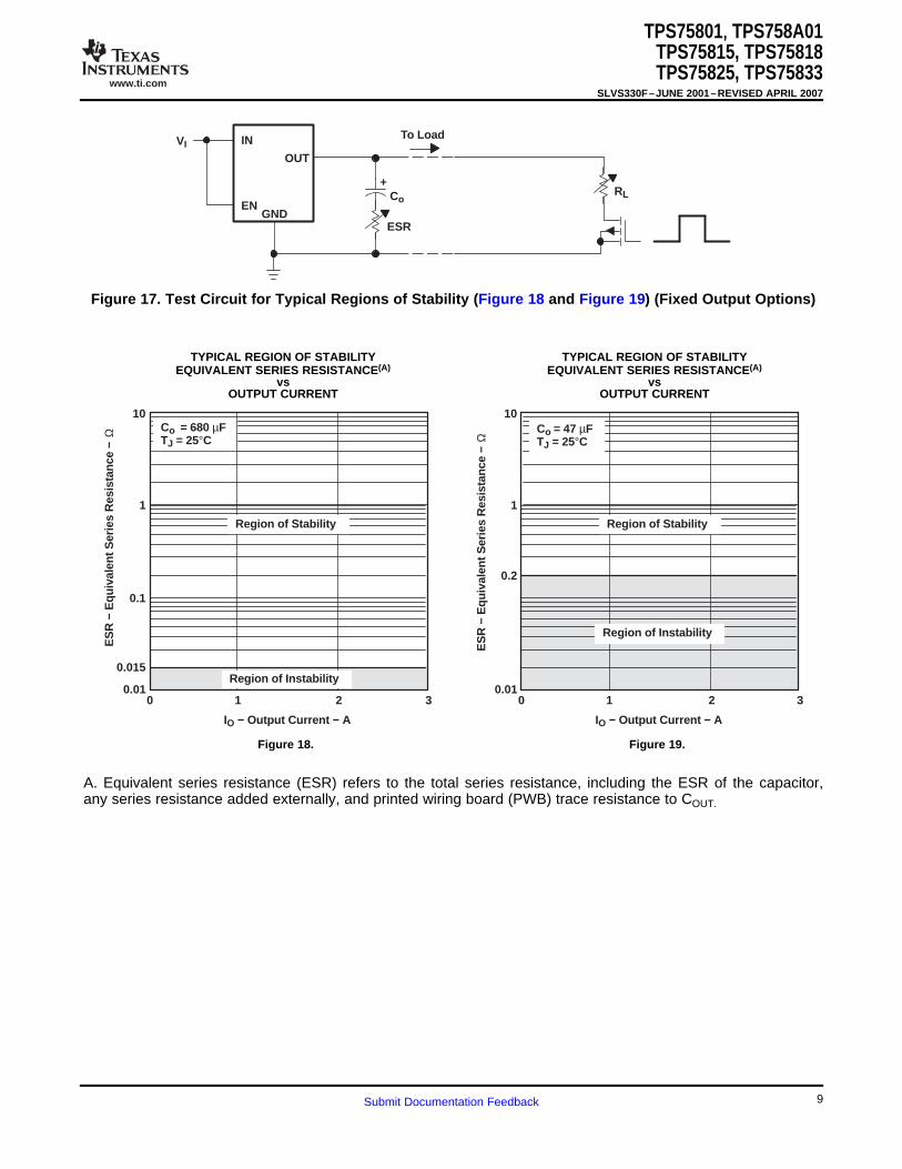
THERMAL INFORMATION
PD max VI(avg)VO(avg) IO(avg)V I(avg) I(Q) (3)
TPS75801,, TPS758A01TPS75815, TPS75818TPS75825, TPS75833SLVS330F–JUNE 2001–REVISED APRIL 2007
APPLICATION INFORMATION (continued)
Figure 21. Output Capacitance vs Equivalent Series Resistance
The amount of heat that an LDO linear regulator generates is directly proportional to the amount of power itdissipates during operation. All integrated circuits have a maximum allowable junction temperature (TJmax)above which normal operation is not assured. A system designer must design the operating environment so thatthe operating junction temperature (TJ) does not exceed the maximum junction temperature (TJmax). The twomain environmental variables that a designer can use to improve thermal performance are air flow and externalheatsinks. The purpose of this information is to aid the designer in determining the proper operating environmentfor a linear regulator that is operating at a specific power level.
In general, the maximum expected power (PD(max)) consumed by a linear regulator is computed as:
Where:• VI(avg) is the average input voltage.• VO(avg) is the average output voltage.• IO(avg) is the average output current.• I(Q) is the quiescent current.
For most TI LDO regulators, the quiescent current is insignificant compared to the average output current;therefore, the term VI(avg)× I(Q) can be neglected. The operating junction temperature is computed by adding theambient temperature (TA) and the increase in temperature due to the regulator power dissipation. Thetemperature rise is computed by multiplying the maximum expected power dissipation by the sum of the thermalresistances between the junction and the case (RΘJC), the case to heatsink (RΘCS), and the heatsink to ambient(RΘSA). Thermal resistances are measures of how effectively an object dissipates heat. Typically, the larger thedevice, the more surface area available for power dissipation and the lower the object's thermal resistance.
Figure 22 illustrates these thermal resistances for (a) a TO-220 package attached to a heatsink, and (b) aTO-263 package mounted on a JEDEC High-K board.
12 Submit Documentation Feedback
www.ti.com
A
B
C
A
B
C
TJA
RθJC
TCB
RθCS
TA
C
RθSA
(a) (b)TO−263 PackageTO−220 Package
TJ TAPD max RJCR
CSRSA
(4)
TJ TAPD maxRJA (5)
RJATJTA
PD max (6)
TPS75801,, TPS758A01TPS75815, TPS75818TPS75825, TPS75833
SLVS330F–JUNE 2001–REVISED APRIL 2007
THERMAL INFORMATION (continued)
Figure 22. Thermal Resistances
Equation 4 summarizes the computation:
The RΘJC is specific to each regulator as determined by its package, lead frame, and die size provided in theregulator's data sheet. The RΘSA is a function of the type and size of heatsink. For example, black body radiatortype heatsinks, like the one attached to the TO-220 package in Figure 22(a), can have RΘCS values ranging from5°C/W for very large heatsinks to 50°C/W for very small heatsinks. The RΘCS is a function of how the package isattached to the heatsink. For example, if a thermal compound is used to attach a heatsink to a TO-220 package,RΘCSof 1°C/W is reasonable.
Even if no external black body radiator type heatsink is attached to the package, the board on which theregulator is mounted will provide some heatsinking through the pin solder connections. Some packages, like theTO-263 and TI's TSSOP PowerPAD™ packages, use a copper plane underneath the package or the circuitboard ground plane for additional heatsinking to improve their thermal performance. Computer-aided thermalmodeling can be used to compute very accurate approximations of integrated circuit thermal performance indifferent operating environments (for example, different types of circuit boards, different types and sizes ofheatsinks, different air flows, etc.). Using these models, the three thermal resistances can be combined into onethermal resistance between junction and ambient (RΘJA). This RΘJAis valid only for the specific operatingenvironment used in the computer model.
Equation 4 simplifies into Equation 5:
Rearranging Equation 5 results in Equation 6:
Using Equation 5 and the computer model generated curves shown in Figure 23 and Figure 26, a designer canquickly compute the required heatsink thermal resistance/board area for a given ambient temperature, powerdissipation, and operating environment.
13Submit Documentation Feedback

www.ti.com
TO-220 Power Dissipation
PD max (3.3 2.5) V 3A 2.4W (7)
RJA max (125 55)C
2.4W 29CW
(8)
5
15
25
35
45
55
65
0510152025RθSA − Heatsink Thermal Resistance − °C/W
− T
herm
al R
esis
tanc
e −
θJA
RC
/W°
No Heatsink
Natural Convection
Air Flow = 150 LFM
Air Flow = 250 LFM
Air Flow = 500 LFM
TPS75801,, TPS758A01TPS75815, TPS75818TPS75825, TPS75833SLVS330F–JUNE 2001–REVISED APRIL 2007
THERMAL INFORMATION (continued)
The TO-220 package provides an effective means of managing power dissipation in through-hole applications.The TO-220 package dimensions are provided in the mechanical drawings at the end of this data sheet. Aheatsink can be used with the TO-220 package to effectively lower the junction-to-ambient thermal resistance.
To illustrate, the TPS75825 in a TO-220 package was chosen. For this example, the average input voltage is3.3V, the average output voltage is 2.5V, the average output current is 3A, the ambient temperature +55°C, theair flow is 150 LFM, and the operating environment is the same as documented below. Neglecting the quiescentcurrent, the maximum average power is:
Substituting TJmax for TJ in Equation 6 results in Equation 8:
From Figure 23, RΘJA vs Heatsink Thermal Resistance, a heatsink with RΘSA = 22°C/W is required to dissipate2.4W. The model operating environment used in the computer model to construct Figure 23 consisted of astandard JEDEC High-K board (2S2P) with a 1-ounce internal copper plane and ground plane. Since thepackage pins were soldered to the board, 450mm2 of the board was modeled as a heatsink. Figure 24 showsthe side view of the operating environment used in the computer model.
Figure 23. Thermal Resistance vs Heatsink Thermal Resistance
14 Submit Documentation Feedback

www.ti.com
1 oz. CopperPower Plane1 oz. Copper
Ground Plane
0.21 mm 0.21 mm
1
10
01020
− P
ower
Dis
sipa
tion
Lim
it −
WP
D
RθSA − Heatsink Thermal Resistance − °C/W
No Heatsink
TA = 55°C
Natural Convection
Air Flow = 150 LFM
Air Flow = 250 LFM
Air Flow = 500 LFM
TPS75801,, TPS758A01TPS75815, TPS75818TPS75825, TPS75833
SLVS330F–JUNE 2001–REVISED APRIL 2007
THERMAL INFORMATION (continued)
Figure 24. TO-220 Thermal Resistance
From the data in Figure 23 and rearranging Equation 6, the maximum power dissipation for a different heatsinkRΘSA and a specific ambient temperature can be computed (see Figure 25).
Figure 25. Power Dissipation vs Heatsink Thermal Resistance
15Submit Documentation Feedback

www.ti.com
TO-263 Power Dissipation
PD max (3.3 2.5) V 3A 2.4W (9)
RJA max (125 55)C
2.4W 29CW
(10)
15
20
25
30
35
40
0 0.01 0.1 1 10 100Copper Heatsink Area − cm 2
− T
herm
al R
esis
tanc
e −
θJA
RC
/W°
No Air Flow
150 LFM
250 LFM
TPS75801,, TPS758A01TPS75815, TPS75818TPS75825, TPS75833SLVS330F–JUNE 2001–REVISED APRIL 2007
THERMAL INFORMATION (continued)
The TO-263 package provides an effective means of managing power dissipation in surface-mount applications.The TO-263 package dimensions are provided in the mechanical drawings at the end of the data sheet. Theaddition of a copper plane directly underneath the TO-263 package enhances the thermal performance of thepackage.
To illustrate, the TPS75825 in a TO-263 package was chosen. For this example, the average input voltage is3.3V, the average output voltage is 2.5V, the average output current is 3A, the ambient temperature +55°C, theair flow is 150 LFM, and the operating environment is the same as documented below. Neglecting the quiescentcurrent, the maximum average power is:
Substituting TJmax for TJ in Equation 6 results in Equation 10:
From Figure 26, RΘJA vs Copper Heatsink Area, the ground plane needs to be 2cm2 for the part to dissipate2.4W. The model operating environment used in the computer model to construct Figure 26 consisted of astandard JEDEC High-K board (2S2P) with a 1-ounce internal copper plane and ground plane. The package issoldered to a 2-ounce copper pad. The pad is tied through thermal vias to the 1-ounce ground plane. Figure 27shows the side view of the operating environment used in the computer model.
Figure 26. Thermal Resistance vs Copper Heatsink Area
16 Submit Documentation Feedback

www.ti.com
1 oz. CopperPower Plane
1 oz. CopperGround Plane
2 oz. Copper Solder PadWith 25 Thermal Vias
Thermal Vias, 0.3 mmDiameter, 1.5 mm Pitch
1
2
3
4
5
0 0.01 0.1 1 10 100
− M
axim
um P
ower
Dis
sipa
tion
− W
PD
Copper Heatsink Area − cm 2
TA = 55°C
No Air Flow
150 LFM
250 LFM
TPS75801,, TPS758A01TPS75815, TPS75818TPS75825, TPS75833
SLVS330F–JUNE 2001–REVISED APRIL 2007
THERMAL INFORMATION (continued)
Figure 27. TO-263 Thermal Resistance
The maximum power dissipation for a different ground plane area and a specific ambient temperature can becomputed from the data in Figure 26 and from rearranging Equation 6 (see Figure 28).
Figure 28. Maximum Power Dissipation vs Copper Heatsink Area
17Submit Documentation Feedback

PACKAGE OPTION ADDENDUM
www.ti.com 15-Apr-2017
Addendum-Page 1
PACKAGING INFORMATION
Orderable Device Status(1)
Package Type PackageDrawing
Pins PackageQty
Eco Plan(2)
Lead/Ball Finish(6)
MSL Peak Temp(3)
Op Temp (°C) Device Marking(4/5)
Samples
TPS75801KC ACTIVE TO-220 KC 5 50 Green (RoHS& no Sb/Br)
CU SN N / A for Pkg Type -40 to 85 75801
TPS75801KTTR ACTIVE DDPAK/TO-263
KTT 5 500 Green (RoHS& no Sb/Br)
CU SN Level-2-260C-1 YEAR -40 to 85 75801
TPS75801KTTRG3 ACTIVE DDPAK/TO-263
KTT 5 500 Green (RoHS& no Sb/Br)
CU SN Level-2-260C-1 YEAR -40 to 85 75801
TPS75801KTTT ACTIVE DDPAK/TO-263
KTT 5 50 Green (RoHS& no Sb/Br)
CU SN Level-2-260C-1 YEAR -40 to 85 75801
TPS75801KTTTG3 ACTIVE DDPAK/TO-263
KTT 5 50 Green (RoHS& no Sb/Br)
CU SN Level-2-260C-1 YEAR -40 to 85 75801
TPS75815KC ACTIVE TO-220 KC 5 50 Green (RoHS& no Sb/Br)
CU SN N / A for Pkg Type -40 to 85 75815
TPS75815KTTR ACTIVE DDPAK/TO-263
KTT 5 500 Green (RoHS& no Sb/Br)
CU SN Level-2-260C-1 YEAR -40 to 85 75815
TPS75815KTTT ACTIVE DDPAK/TO-263
KTT 5 50 Green (RoHS& no Sb/Br)
CU SN Level-2-260C-1 YEAR 75815
TPS75815KTTTG3 ACTIVE DDPAK/TO-263
KTT 5 50 Green (RoHS& no Sb/Br)
CU SN Level-2-260C-1 YEAR 75815
TPS75818KC ACTIVE TO-220 KC 5 50 Green (RoHS& no Sb/Br)
CU SN N / A for Pkg Type -40 to 85 75818
TPS75818KTTR ACTIVE DDPAK/TO-263
KTT 5 500 Green (RoHS& no Sb/Br)
CU SN Level-2-260C-1 YEAR -40 to 85 75818
TPS75818KTTRG3 ACTIVE DDPAK/TO-263
KTT 5 500 Green (RoHS& no Sb/Br)
CU SN Level-2-260C-1 YEAR -40 to 85 75818
TPS75818KTTT ACTIVE DDPAK/TO-263
KTT 5 50 Green (RoHS& no Sb/Br)
CU SN Level-2-260C-1 YEAR 75818
TPS75818KTTTG3 ACTIVE DDPAK/TO-263
KTT 5 50 Green (RoHS& no Sb/Br)
CU SN Level-2-260C-1 YEAR 75818
TPS75825KC ACTIVE TO-220 KC 5 50 Green (RoHS& no Sb/Br)
CU SN N / A for Pkg Type -40 to 85 75825
TPS75825KTTR ACTIVE DDPAK/TO-263
KTT 5 500 Green (RoHS& no Sb/Br)
CU SN Level-2-260C-1 YEAR -40 to 85 75825
TPS75825KTTRG3 ACTIVE DDPAK/TO-263
KTT 5 500 Green (RoHS& no Sb/Br)
CU SN Level-2-260C-1 YEAR -40 to 85 75825

PACKAGE OPTION ADDENDUM
www.ti.com 15-Apr-2017
Addendum-Page 2
Orderable Device Status(1)
Package Type PackageDrawing
Pins PackageQty
Eco Plan(2)
Lead/Ball Finish(6)
MSL Peak Temp(3)
Op Temp (°C) Device Marking(4/5)
Samples
TPS75825KTTT ACTIVE DDPAK/TO-263
KTT 5 50 Green (RoHS& no Sb/Br)
CU SN Level-2-260C-1 YEAR 75825
TPS75825KTTTG3 ACTIVE DDPAK/TO-263
KTT 5 50 Green (RoHS& no Sb/Br)
CU SN Level-2-260C-1 YEAR 75825
TPS75833KC ACTIVE TO-220 KC 5 50 Green (RoHS& no Sb/Br)
CU SN N / A for Pkg Type -40 to 85 75833
TPS75833KCG3 ACTIVE TO-220 KC 5 50 Green (RoHS& no Sb/Br)
CU SN N / A for Pkg Type -40 to 85 75833
TPS75833KTTR ACTIVE DDPAK/TO-263
KTT 5 500 Green (RoHS& no Sb/Br)
CU SN Level-2-260C-1 YEAR -40 to 85 75833
TPS75833KTTT ACTIVE DDPAK/TO-263
KTT 5 50 Green (RoHS& no Sb/Br)
CU SN Level-2-260C-1 YEAR 75833
TPS75833KTTTG3 ACTIVE DDPAK/TO-263
KTT 5 50 Green (RoHS& no Sb/Br)
CU SN Level-2-260C-1 YEAR 75833
TPS758A01KTTR ACTIVE DDPAK/TO-263
KTT 5 500 Green (RoHS& no Sb/Br)
CU SN Level-2-260C-1 YEAR -40 to 125 758A01
TPS758A01KTTT ACTIVE DDPAK/TO-263
KTT 5 50 Green (RoHS& no Sb/Br)
CU SN Level-2-260C-1 YEAR -40 to 125 758A01
(1) The marketing status values are defined as follows:ACTIVE: Product device recommended for new designs.LIFEBUY: TI has announced that the device will be discontinued, and a lifetime-buy period is in effect.NRND: Not recommended for new designs. Device is in production to support existing customers, but TI does not recommend using this part in a new design.PREVIEW: Device has been announced but is not in production. Samples may or may not be available.OBSOLETE: TI has discontinued the production of the device.
(2) Eco Plan - The planned eco-friendly classification: Pb-Free (RoHS), Pb-Free (RoHS Exempt), or Green (RoHS & no Sb/Br) - please check http://www.ti.com/productcontent for the latest availabilityinformation and additional product content details.TBD: The Pb-Free/Green conversion plan has not been defined.Pb-Free (RoHS): TI's terms "Lead-Free" or "Pb-Free" mean semiconductor products that are compatible with the current RoHS requirements for all 6 substances, including the requirement thatlead not exceed 0.1% by weight in homogeneous materials. Where designed to be soldered at high temperatures, TI Pb-Free products are suitable for use in specified lead-free processes.Pb-Free (RoHS Exempt): This component has a RoHS exemption for either 1) lead-based flip-chip solder bumps used between the die and package, or 2) lead-based die adhesive used betweenthe die and leadframe. The component is otherwise considered Pb-Free (RoHS compatible) as defined above.Green (RoHS & no Sb/Br): TI defines "Green" to mean Pb-Free (RoHS compatible), and free of Bromine (Br) and Antimony (Sb) based flame retardants (Br or Sb do not exceed 0.1% by weightin homogeneous material)
(3) MSL, Peak Temp. - The Moisture Sensitivity Level rating according to the JEDEC industry standard classifications, and peak solder temperature.

PACKAGE OPTION ADDENDUM
www.ti.com 15-Apr-2017
Addendum-Page 3
(4) There may be additional marking, which relates to the logo, the lot trace code information, or the environmental category on the device.
(5) Multiple Device Markings will be inside parentheses. Only one Device Marking contained in parentheses and separated by a "~" will appear on a device. If a line is indented then it is a continuationof the previous line and the two combined represent the entire Device Marking for that device.
(6) Lead/Ball Finish - Orderable Devices may have multiple material finish options. Finish options are separated by a vertical ruled line. Lead/Ball Finish values may wrap to two lines if the finishvalue exceeds the maximum column width.
Important Information and Disclaimer:The information provided on this page represents TI's knowledge and belief as of the date that it is provided. TI bases its knowledge and belief on informationprovided by third parties, and makes no representation or warranty as to the accuracy of such information. Efforts are underway to better integrate information from third parties. TI has taken andcontinues to take reasonable steps to provide representative and accurate information but may not have conducted destructive testing or chemical analysis on incoming materials and chemicals.TI and TI suppliers consider certain information to be proprietary, and thus CAS numbers and other limited information may not be available for release.
In no event shall TI's liability arising out of such information exceed the total purchase price of the TI part(s) at issue in this document sold by TI to Customer on an annual basis.

TAPE AND REEL INFORMATION
*All dimensions are nominal
Device PackageType
PackageDrawing
Pins SPQ ReelDiameter
(mm)
ReelWidth
W1 (mm)
A0(mm)
B0(mm)
K0(mm)
P1(mm)
W(mm)
Pin1Quadrant
TPS75801KTTR DDPAK/TO-263
KTT 5 500 330.0 24.4 10.6 15.6 4.9 16.0 24.0 Q2
TPS75801KTTT DDPAK/TO-263
KTT 5 50 330.0 24.4 10.6 15.6 4.9 16.0 24.0 Q2
TPS75815KTTR DDPAK/TO-263
KTT 5 500 330.0 24.4 10.6 15.6 4.9 16.0 24.0 Q2
TPS75815KTTT DDPAK/TO-263
KTT 5 50 330.0 24.4 10.6 15.6 4.9 16.0 24.0 Q2
TPS75818KTTR DDPAK/TO-263
KTT 5 500 330.0 24.4 10.6 15.6 4.9 16.0 24.0 Q2
TPS75818KTTT DDPAK/TO-263
KTT 5 50 330.0 24.4 10.6 15.6 4.9 16.0 24.0 Q2
TPS75825KTTR DDPAK/TO-263
KTT 5 500 330.0 24.4 10.6 15.6 4.9 16.0 24.0 Q2
TPS75825KTTT DDPAK/TO-263
KTT 5 50 330.0 24.4 10.6 15.6 4.9 16.0 24.0 Q2
TPS75833KTTR DDPAK/TO-263
KTT 5 500 330.0 24.4 10.6 15.6 4.9 16.0 24.0 Q2
TPS75833KTTT DDPAK/TO-263
KTT 5 50 330.0 24.4 10.6 15.6 4.9 16.0 24.0 Q2
TPS758A01KTTR DDPAK/ KTT 5 500 330.0 24.4 10.6 15.6 4.9 16.0 24.0 Q2
PACKAGE MATERIALS INFORMATION
www.ti.com 12-Feb-2016
Pack Materials-Page 1

Device PackageType
PackageDrawing
Pins SPQ ReelDiameter
(mm)
ReelWidth
W1 (mm)
A0(mm)
B0(mm)
K0(mm)
P1(mm)
W(mm)
Pin1Quadrant
TO-263
TPS758A01KTTT DDPAK/TO-263
KTT 5 50 330.0 24.4 10.6 15.6 4.9 16.0 24.0 Q2
*All dimensions are nominal
Device Package Type Package Drawing Pins SPQ Length (mm) Width (mm) Height (mm)
TPS75801KTTR DDPAK/TO-263 KTT 5 500 367.0 367.0 45.0
TPS75801KTTT DDPAK/TO-263 KTT 5 50 367.0 367.0 45.0
TPS75815KTTR DDPAK/TO-263 KTT 5 500 367.0 367.0 45.0
TPS75815KTTT DDPAK/TO-263 KTT 5 50 367.0 367.0 45.0
TPS75818KTTR DDPAK/TO-263 KTT 5 500 367.0 367.0 45.0
TPS75818KTTT DDPAK/TO-263 KTT 5 50 367.0 367.0 45.0
TPS75825KTTR DDPAK/TO-263 KTT 5 500 367.0 367.0 45.0
TPS75825KTTT DDPAK/TO-263 KTT 5 50 367.0 367.0 45.0
TPS75833KTTR DDPAK/TO-263 KTT 5 500 367.0 367.0 45.0
TPS75833KTTT DDPAK/TO-263 KTT 5 50 367.0 367.0 45.0
TPS758A01KTTR DDPAK/TO-263 KTT 5 500 367.0 367.0 45.0
TPS758A01KTTT DDPAK/TO-263 KTT 5 50 367.0 367.0 45.0
PACKAGE MATERIALS INFORMATION
www.ti.com 12-Feb-2016
Pack Materials-Page 2

www.ti.com
PACKAGE OUTLINE
C
B
9.257.67
6.865.69
3.052.54
14.7312.29
5X 1.020.64
4X 1.7
8.896.86
12.8810.08
(6.275)
4.834.06
1.401.14
3.052.03
0.610.30
-3.963.71
6.8
2X (R1)OPTIONAL
16.51MAX
A10.679.65
(4.25)
4215009/A 01/2017
TO-220 - 16.51 mm max heightKC0005ATO-220
NOTES: 1. All controlling linear dimensions are in inches. Dimensions in brackets are in millimeters. Any dimension in brackets or parenthesis are for reference only. Dimensioning and tolerancing per ASME Y14.5M.2. This drawing is subject to change without notice.3. Shape may vary per different assembly sites.
0.25 C A B
PIN 1 ID(OPTIONAL)
1 5
OPTIONALCHAMFER
SCALE 0.850
NOTE 3
1 5
AAAA
www.ti.com
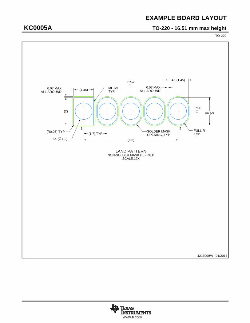
EXAMPLE BOARD LAYOUT
0.07 MAXALL AROUND
0.07 MAXALL AROUND (1.45)
(2)
(R0.05) TYP
4X (1.45)
4X (2)
5X ( 1.2)(1.7) TYP
(6.8)
FULL RTYP
TO-220 - 16.51 mm max heightKC0005ATO-220
4215009/A 01/2017
LAND PATTERNNON-SOLDER MASK DEFINED
SCALE:12X
PKG
PKG
METALTYP
SOLDER MASKOPENING, TYP
1 5


IMPORTANT NOTICE
Texas Instruments Incorporated (TI) reserves the right to make corrections, enhancements, improvements and other changes to itssemiconductor products and services per JESD46, latest issue, and to discontinue any product or service per JESD48, latest issue. Buyersshould obtain the latest relevant information before placing orders and should verify that such information is current and complete.TI’s published terms of sale for semiconductor products (http://www.ti.com/sc/docs/stdterms.htm) apply to the sale of packaged integratedcircuit products that TI has qualified and released to market. Additional terms may apply to the use or sale of other types of TI products andservices.Reproduction of significant portions of TI information in TI data sheets is permissible only if reproduction is without alteration and isaccompanied by all associated warranties, conditions, limitations, and notices. TI is not responsible or liable for such reproduceddocumentation. Information of third parties may be subject to additional restrictions. Resale of TI products or services with statementsdifferent from or beyond the parameters stated by TI for that product or service voids all express and any implied warranties for theassociated TI product or service and is an unfair and deceptive business practice. TI is not responsible or liable for any such statements.Buyers and others who are developing systems that incorporate TI products (collectively, “Designers”) understand and agree that Designersremain responsible for using their independent analysis, evaluation and judgment in designing their applications and that Designers havefull and exclusive responsibility to assure the safety of Designers' applications and compliance of their applications (and of all TI productsused in or for Designers’ applications) with all applicable regulations, laws and other applicable requirements. Designer represents that, withrespect to their applications, Designer has all the necessary expertise to create and implement safeguards that (1) anticipate dangerousconsequences of failures, (2) monitor failures and their consequences, and (3) lessen the likelihood of failures that might cause harm andtake appropriate actions. Designer agrees that prior to using or distributing any applications that include TI products, Designer willthoroughly test such applications and the functionality of such TI products as used in such applications.TI’s provision of technical, application or other design advice, quality characterization, reliability data or other services or information,including, but not limited to, reference designs and materials relating to evaluation modules, (collectively, “TI Resources”) are intended toassist designers who are developing applications that incorporate TI products; by downloading, accessing or using TI Resources in anyway, Designer (individually or, if Designer is acting on behalf of a company, Designer’s company) agrees to use any particular TI Resourcesolely for this purpose and subject to the terms of this Notice.TI’s provision of TI Resources does not expand or otherwise alter TI’s applicable published warranties or warranty disclaimers for TIproducts, and no additional obligations or liabilities arise from TI providing such TI Resources. TI reserves the right to make corrections,enhancements, improvements and other changes to its TI Resources. TI has not conducted any testing other than that specificallydescribed in the published documentation for a particular TI Resource.Designer is authorized to use, copy and modify any individual TI Resource only in connection with the development of applications thatinclude the TI product(s) identified in such TI Resource. NO OTHER LICENSE, EXPRESS OR IMPLIED, BY ESTOPPEL OR OTHERWISETO ANY OTHER TI INTELLECTUAL PROPERTY RIGHT, AND NO LICENSE TO ANY TECHNOLOGY OR INTELLECTUAL PROPERTYRIGHT OF TI OR ANY THIRD PARTY IS GRANTED HEREIN, including but not limited to any patent right, copyright, mask work right, orother intellectual property right relating to any combination, machine, or process in which TI products or services are used. Informationregarding or referencing third-party products or services does not constitute a license to use such products or services, or a warranty orendorsement thereof. Use of TI Resources may require a license from a third party under the patents or other intellectual property of thethird party, or a license from TI under the patents or other intellectual property of TI.TI RESOURCES ARE PROVIDED “AS IS” AND WITH ALL FAULTS. TI DISCLAIMS ALL OTHER WARRANTIES ORREPRESENTATIONS, EXPRESS OR IMPLIED, REGARDING RESOURCES OR USE THEREOF, INCLUDING BUT NOT LIMITED TOACCURACY OR COMPLETENESS, TITLE, ANY EPIDEMIC FAILURE WARRANTY AND ANY IMPLIED WARRANTIES OFMERCHANTABILITY, FITNESS FOR A PARTICULAR PURPOSE, AND NON-INFRINGEMENT OF ANY THIRD PARTY INTELLECTUALPROPERTY RIGHTS. TI SHALL NOT BE LIABLE FOR AND SHALL NOT DEFEND OR INDEMNIFY DESIGNER AGAINST ANY CLAIM,INCLUDING BUT NOT LIMITED TO ANY INFRINGEMENT CLAIM THAT RELATES TO OR IS BASED ON ANY COMBINATION OFPRODUCTS EVEN IF DESCRIBED IN TI RESOURCES OR OTHERWISE. IN NO EVENT SHALL TI BE LIABLE FOR ANY ACTUAL,DIRECT, SPECIAL, COLLATERAL, INDIRECT, PUNITIVE, INCIDENTAL, CONSEQUENTIAL OR EXEMPLARY DAMAGES INCONNECTION WITH OR ARISING OUT OF TI RESOURCES OR USE THEREOF, AND REGARDLESS OF WHETHER TI HAS BEENADVISED OF THE POSSIBILITY OF SUCH DAMAGES.Unless TI has explicitly designated an individual product as meeting the requirements of a particular industry standard (e.g., ISO/TS 16949and ISO 26262), TI is not responsible for any failure to meet such industry standard requirements.Where TI specifically promotes products as facilitating functional safety or as compliant with industry functional safety standards, suchproducts are intended to help enable customers to design and create their own applications that meet applicable functional safety standardsand requirements. Using products in an application does not by itself establish any safety features in the application. Designers mustensure compliance with safety-related requirements and standards applicable to their applications. Designer may not use any TI products inlife-critical medical equipment unless authorized officers of the parties have executed a special contract specifically governing such use.Life-critical medical equipment is medical equipment where failure of such equipment would cause serious bodily injury or death (e.g., lifesupport, pacemakers, defibrillators, heart pumps, neurostimulators, and implantables). Such equipment includes, without limitation, allmedical devices identified by the U.S. Food and Drug Administration as Class III devices and equivalent classifications outside the U.S.TI may expressly designate certain products as completing a particular qualification (e.g., Q100, Military Grade, or Enhanced Product).Designers agree that it has the necessary expertise to select the product with the appropriate qualification designation for their applicationsand that proper product selection is at Designers’ own risk. Designers are solely responsible for compliance with all legal and regulatoryrequirements in connection with such selection.Designer will fully indemnify TI and its representatives against any damages, costs, losses, and/or liabilities arising out of Designer’s non-compliance with the terms and provisions of this Notice.
Mailing Address: Texas Instruments, Post Office Box 655303, Dallas, Texas 75265Copyright © 2017, Texas Instruments Incorporated