Embed Size (px)
Citation preview
Lecture 20
ANNOUNCEMENTS• HW#11 is due in 2 weeks on 11/20• HW#11 is due in 2 weeks, on 11/20.• Review session: Fri. 11/9, 3‐5PM in 306 Soda (HP Auditorium)• Midterm #2 (Thursday 11/15 in Sibley Auditorium):
• Material of Lectures 11‐18 (HW# 7‐10; Chapters 6,9,11)• 4 pgs of notes (double‐sided, 8.5”×11”), calculator allowed
OUTLINE• Review of MOSFET Amplifiers• MOSFET Cascode Stage• MOSFET Current Mirror
EE105 Fall 2007 Lecture 20, Slide 1 Prof. Liu, UC Berkeley
Reading: Chapter 9
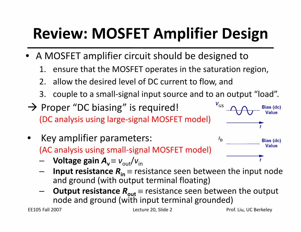
Review: MOSFET Amplifier Design• A MOSFET amplifier circuit should be designed to
1. ensure that the MOSFET operates in the saturation region, p g ,2. allow the desired level of DC current to flow, and3. couple to a small‐signal input source and to an output “load”.
Proper “DC biasing” is required!(DC analysis using large‐signal MOSFET model)
• Key amplifier parameters: (AC analysis using small‐signal MOSFET model)
Voltage gain A ≡ v /v– Voltage gain Av ≡ vout/vin– Input resistance Rin ≡ resistance seen between the input node
and ground (with output terminal floating)O t t i t R i t b t th t t
EE105 Fall 2007 Lecture 20, Slide 2 Prof. Liu, UC Berkeley
– Output resistance Rout ≡ resistance seen between the output node and ground (with input terminal grounded)
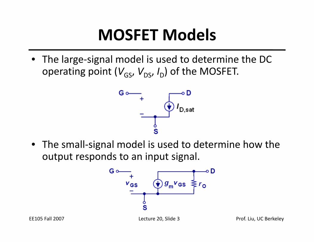
MOSFET Models• The large‐signal model is used to determine the DC operating point (VGS, VDS, ID) of the MOSFET.p g p ( GS, DS, D)
• The small‐signal model is used to determine how the output responds to an input signal.
EE105 Fall 2007 Lecture 20, Slide 3 Prof. Liu, UC Berkeley
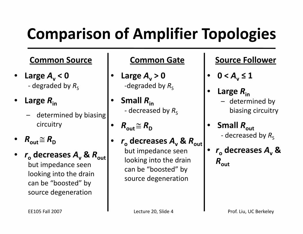
Comparison of Amplifier TopologiesCommon Source
L A 0
Common Gate
L A 0
Source Follower
0 A 1• Large Av < 0‐ degraded by RS
• Large Ri
• Large Av > 0‐degraded by RS
• Small Ri
• 0 < Av ≤ 1
• Large Rin– determined byLarge Rin
– determined by biasing circuitry
Small Rin‐ decreased by RS
• Rout ≅ RD
determined by biasing circuitry
• Small Rout
• Rout ≅ RD
• ro decreases Av & Rout
• ro decreases Av & Routbut impedance seenlooking into the drain
‐ decreased by RS
• ro decreases Av & Rbut impedance seen
looking into the draincan be “boosted” by
d ti
looking into the drain can be “boosted” by source degeneration
Rout
EE105 Fall 2007 Lecture 20, Slide 4 Prof. Liu, UC Berkeley
source degeneration
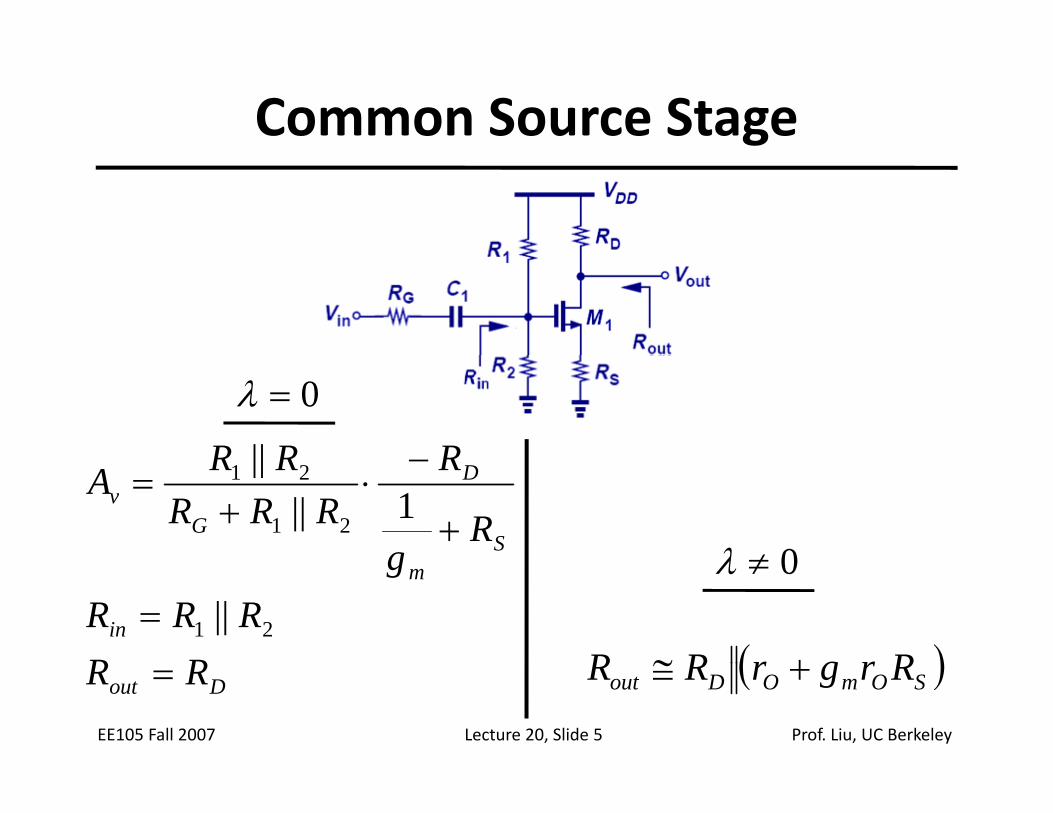
Common Source Stage
RRR ||
0=λ
S
D
Gv
Rg
RRRR
RRA+
−⋅
+=
21
21
1||||
0≠λ
in
m
RRRRR
g= 21 ||
0≠λ
( )RrgrRR +≅
EE105 Fall 2007 Lecture 20, Slide 5 Prof. Liu, UC Berkeley
Dout RR = ( )SOmODout RrgrRR +≅
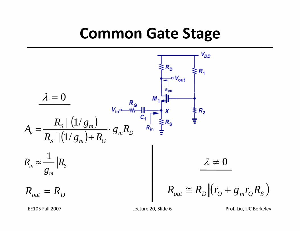
Common Gate Stage
0=λ
( )mS RggRA ⋅=/1||
( ) DmGmS
v RgRgR
A+
=/1||
RR 1 0λSm
in Rg
R ≈
RR ( )RrgrRR +≅
0≠λ
EE105 Fall 2007 Lecture 20, Slide 6 Prof. Liu, UC Berkeley
Dout RR = ( )SOmODout RrgrRR +≅
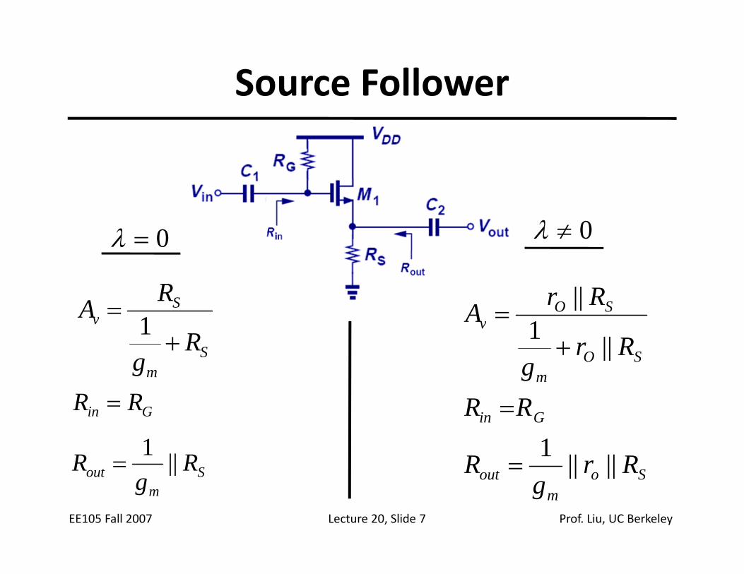
Source Follower
0=λ 0≠λ
Sv
RA = 1SO
vRrA 1
||=
Sm
v
Rg
+1
RR
SOm
v
Rrg
||1+
Gin RR =Gin
RrR
RR
||||1=
=
SRR ||1=
EE105 Fall 2007 Lecture 20, Slide 7 Prof. Liu, UC Berkeley
Som
out Rrg
R ||||=Sm
out Rg
R ||
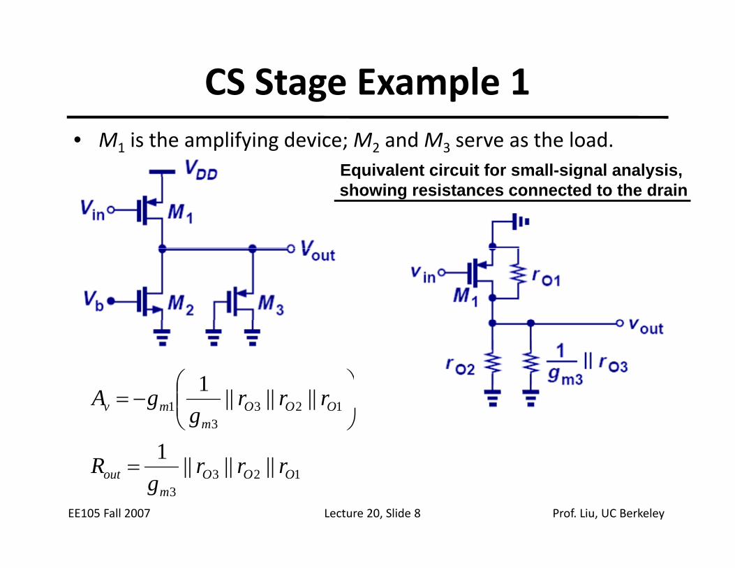
CS Stage Example 1• M1 is the amplifying device; M2 and M3 serve as the load.
Equivalent circuit for small-signal analysis, q g y ,showing resistances connected to the drain
||||||1A⎞
⎜⎛
1233
1
||||||1
|||||| OOOm
mv
rrrR
rrrg
gA⎠
⎜⎜⎝
−=
EE105 Fall 2007 Lecture 20, Slide 8 Prof. Liu, UC Berkeley
1233
|||||| OOOm
out rrrg
R =
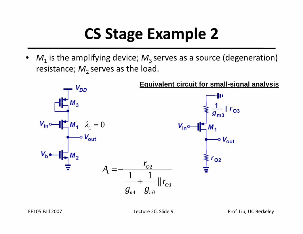
CS Stage Example 2• M1 is the amplifying device; M3 serves as a source (degeneration)
resistance; M2 serves as the load. ; 2
Equivalent circuit for small-signal analysis
01 =λ
331
2
||11O
Ov
rgg
rA+
−=
EE105 Fall 2007 Lecture 20, Slide 9 Prof. Liu, UC Berkeley
31 mm gg
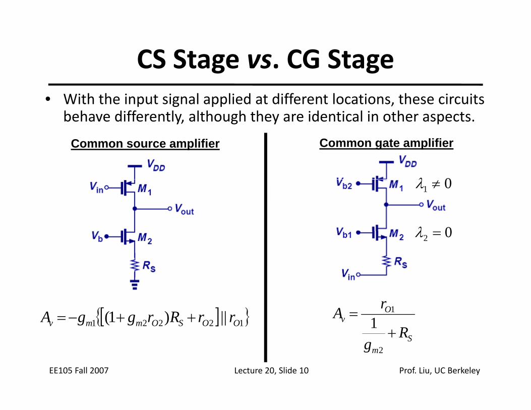
CS Stage vs. CG Stage• With the input signal applied at different locations, these circuits
behave differently, although they are identical in other aspects.
Common source amplifier Common gate amplifier
0λ
0λ
01 ≠λ
02 =λ
Ov
R
rA+
= 1
1[ ]{ }12221 ||)1( OOSOmmv rrRrggA ++−=
EE105 Fall 2007 Lecture 20, Slide 10 Prof. Liu, UC Berkeley
Sm
Rg
+2
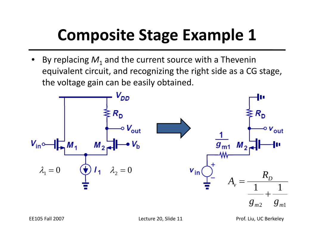
Composite Stage Example 1• By replacing M1 and the current source with a Thevenin
equivalent circuit, and recognizing the right side as a CG stage, q , g g g g ,the voltage gain can be easily obtained.
0λ 0λ
11D
vRA+
=01 =λ 02 =λ
EE105 Fall 2007 Lecture 20, Slide 11 Prof. Liu, UC Berkeley
12 mm gg
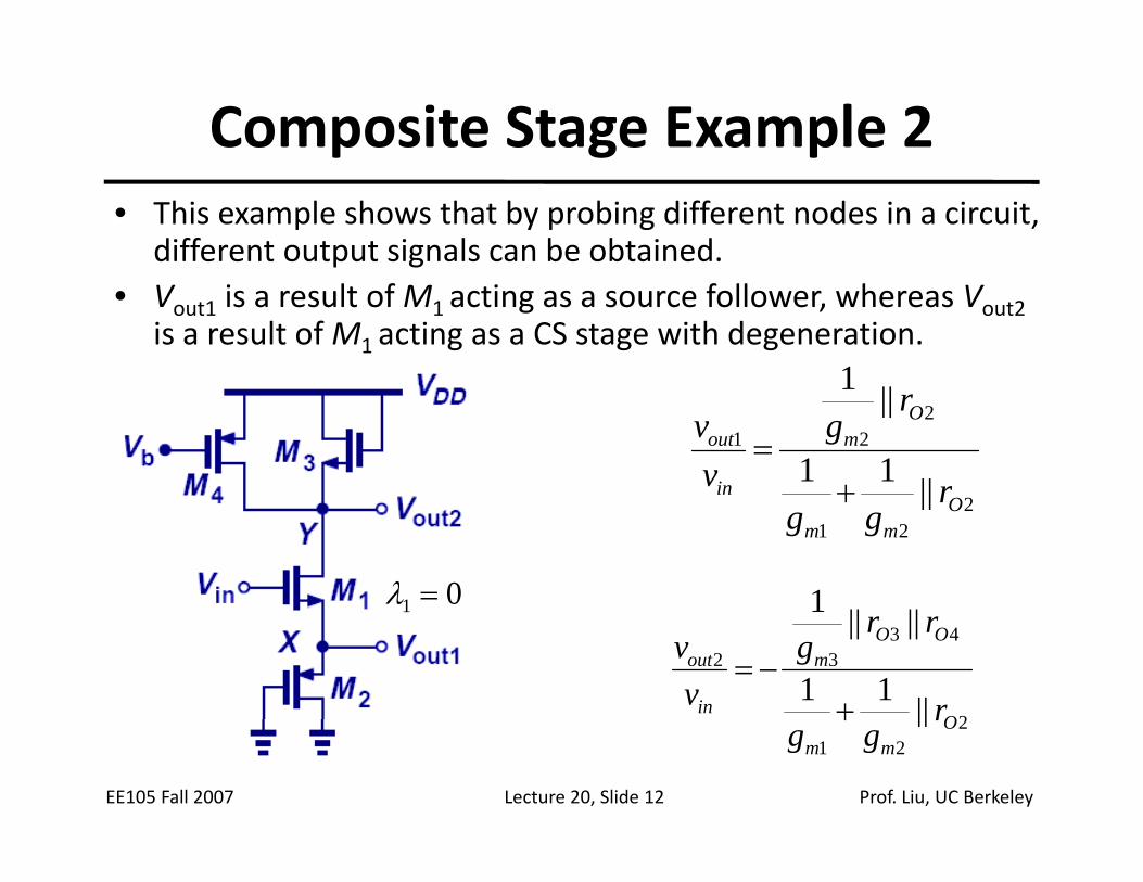
Composite Stage Example 2• This example shows that by probing different nodes in a circuit,
different output signals can be obtained.• Vout1 is a result of M1 acting as a source follower, whereas Vout2
is a result of M1 acting as a CS stage with degeneration.1
221
||11
||1O
m
in
out
r
rg
vv
+=
101 =λ
221
|| Omm
rgg
+
2
4332
||11
||||1
O
OOm
in
out
r
rrg
vv
+−=
1
EE105 Fall 2007 Lecture 20, Slide 12 Prof. Liu, UC Berkeley
221
|| Omm
rgg
+
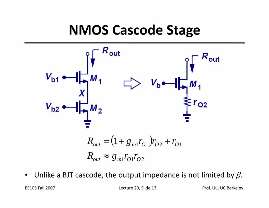
NMOS Cascode Stage
( ) 12111 OOOt rrrgR ++= ( )211
12111
OOmout
OOOmout
rrgRrrrgR
≈++
EE105 Fall 2007 Lecture 20, Slide 13 Prof. Liu, UC Berkeley
• Unlike a BJT cascode, the output impedance is not limited by β.
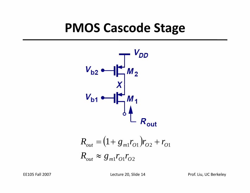
PMOS Cascode Stage
( )211
12111
OO
OOOmout
rrgRrrrgR
≈++=
EE105 Fall 2007 Lecture 20, Slide 14 Prof. Liu, UC Berkeley
211 OOmout rrgR ≈
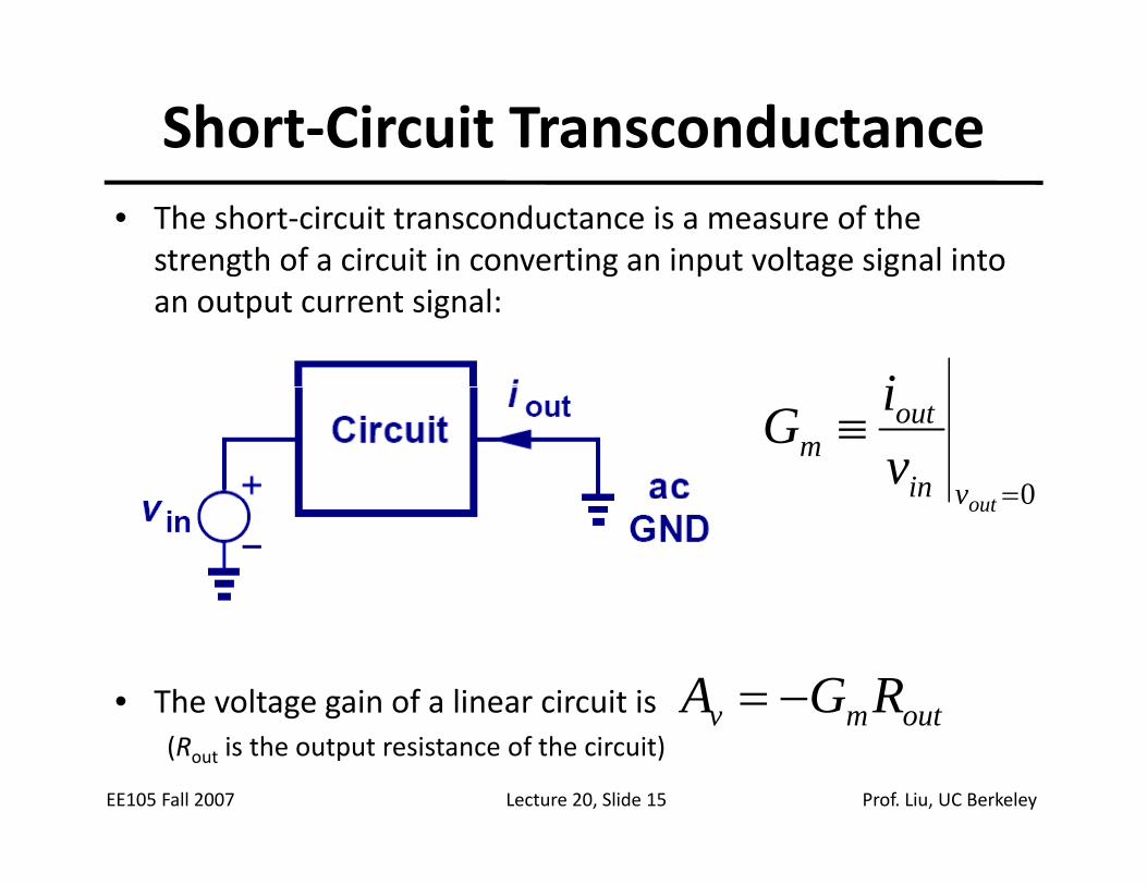
Short‐Circuit Transconductance• The short‐circuit transconductance is a measure of the
strength of a circuit in converting an input voltage signal into g g p g gan output current signal:
i
0=
≡vin
outm v
iG0=outv
• The voltage gain of a linear circuit is outmv RGA −=
EE105 Fall 2007 Lecture 20, Slide 15 Prof. Liu, UC Berkeley
(Rout is the output resistance of the circuit)outmv
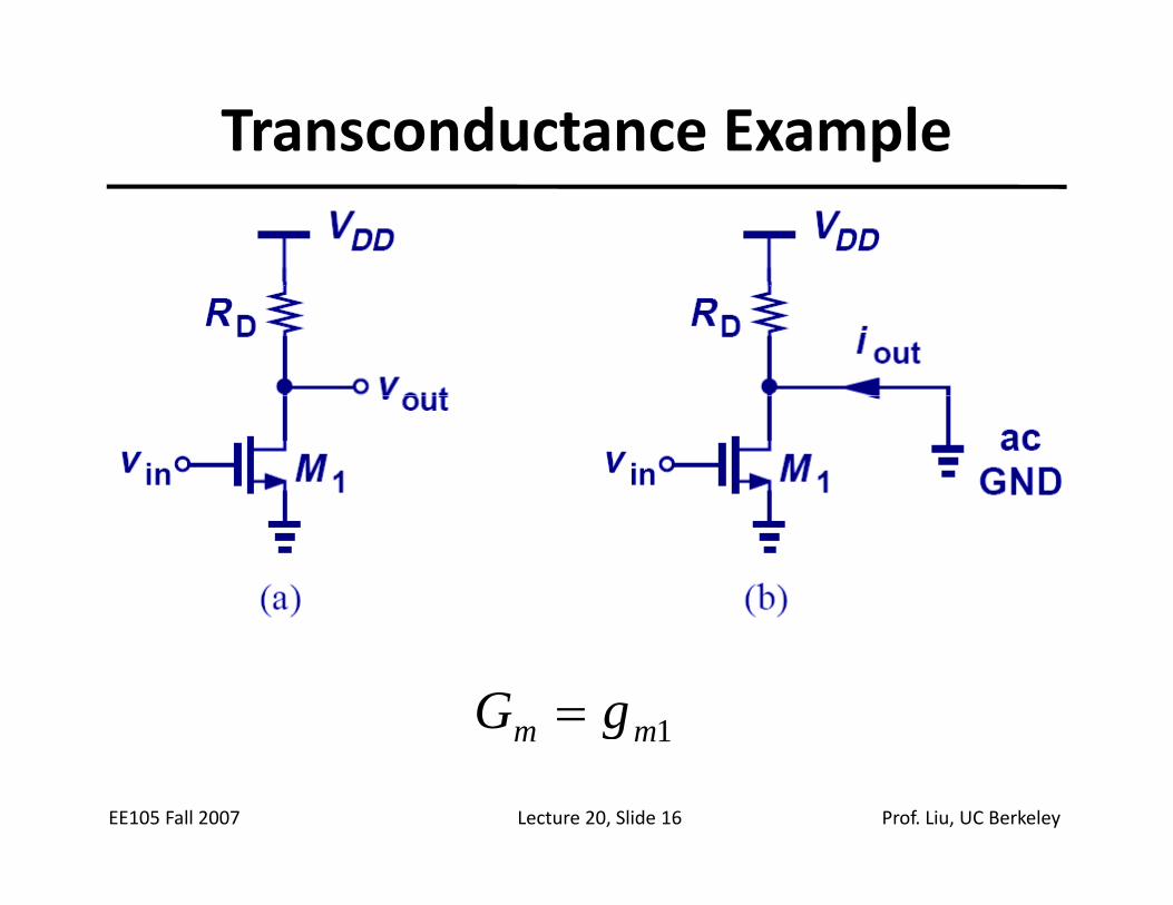
Transconductance Example
1mm gG =
EE105 Fall 2007 Lecture 20, Slide 16 Prof. Liu, UC Berkeley
1mm g
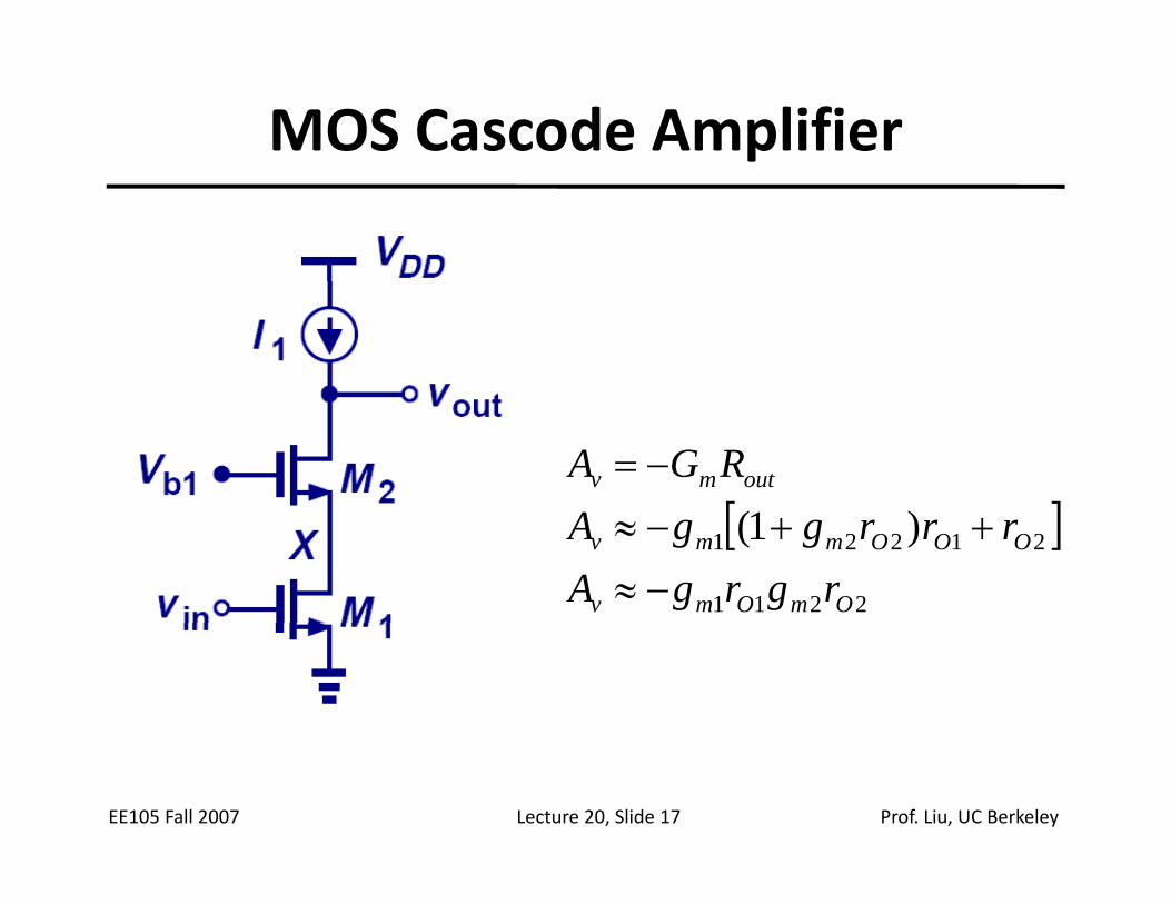
MOS Cascode Amplifier
[ ]outmv RGA −=[ ]
2211
21221 )1(
OmOmv
OOOmmv
rgrgArrrggA
−≈++−≈
EE105 Fall 2007 Lecture 20, Slide 17 Prof. Liu, UC Berkeley
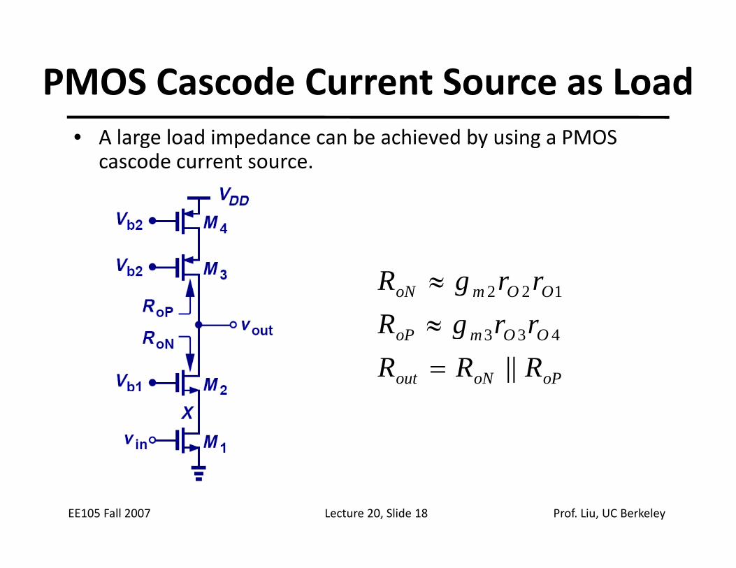
PMOS Cascode Current Source as Load• A large load impedance can be achieved by using a PMOS
cascode current source.
OOmoN
RrrgR 122≈
oPoNout
OOmoP
RRRrrgR
||433
=≈
EE105 Fall 2007 Lecture 20, Slide 18 Prof. Liu, UC Berkeley
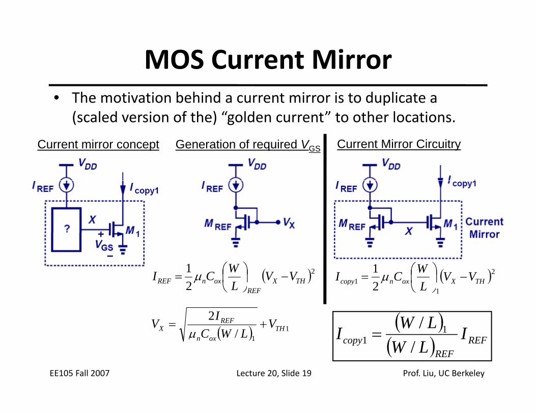
MOS Current Mirror• The motivation behind a current mirror is to duplicate a
(scaled version of the) “golden current” to other locations.
Current mirror concept Generation of required VGS Current Mirror Circuitry
( )221
THXoxnREF VVLWCI −⎟
⎠⎞
⎜⎝⎛= µ ( )21 2
1THXoxncopy VV
LWCI −⎟
⎠⎞
⎜⎝⎛= µ
( )( ) REFILWI / 1
1 =( ) 11/
2TH
REFX V
LWCIV +=
µ
2 REFL ⎠⎝ 12py L ⎠⎝
EE105 Fall 2007 Lecture 20, Slide 19 Prof. Liu, UC Berkeley
( ) REFREF
copy ILW
I/1( )1/oxn LWCµ
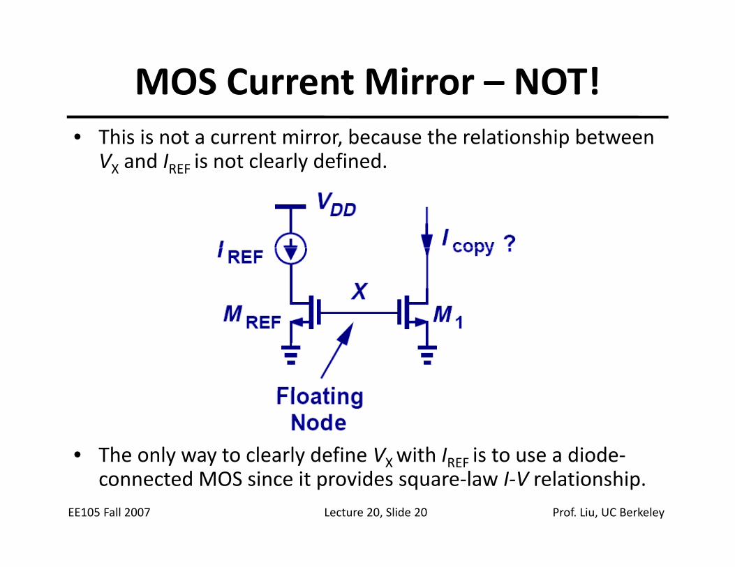
MOS Current Mirror – NOT!• This is not a current mirror, because the relationship between
VX and IREF is not clearly defined.
• The only way to clearly define VXwith IREF is to use a diode‐
EE105 Fall 2007 Lecture 20, Slide 20 Prof. Liu, UC Berkeley
y y y X REF connected MOS since it provides square‐law I‐V relationship.
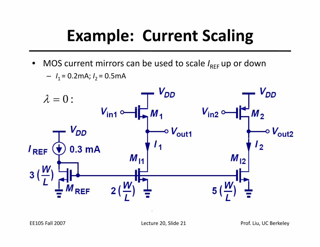
Example: Current Scaling • MOS current mirrors can be used to scale IREF up or down
– I = 0 2mA; I = 0 5mAI1 = 0.2mA; I2 = 0.5mA
:0=λ
EE105 Fall 2007 Lecture 20, Slide 21 Prof. Liu, UC Berkeley
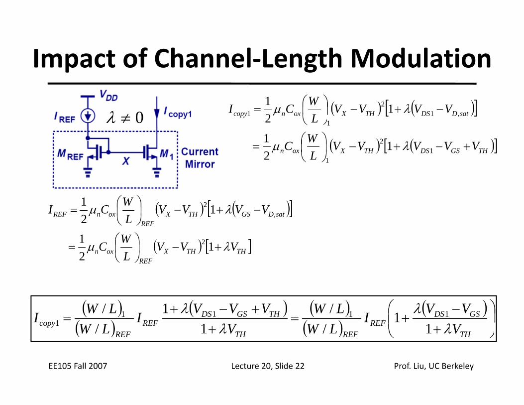
Impact of Channel‐Length Modulation
0≠λ ( ) ( )[ ]satDDSTHXoxncopy VVVVLWCI −+−⎟
⎠⎞
⎜⎝⎛= ,1
2
11 1
21 λµ
( ) ( )[ ]THGSDSTHXoxn VVVVVLWC +−+−⎟
⎠⎞
⎜⎝⎛= 1
2
1
121 λµ
( ) ( )[ ]satDGSTHXREF
oxnREF VVVVLWCI λµ −+−⎟
⎠⎞
⎜⎝⎛= 1
21
,2
( ) [ ]THTHXREF
oxn VVVLWC λµ +−⎟
⎠⎞
⎜⎝⎛= 1
21 2
( )( )
( ) ( )( )
( )⎟⎠
⎞⎜⎜⎝
⎛+
−+=
++−+
= GSDSREF
THGSDSREFcopy V
VVILWLW
VVVVI
LWLWI
λλ
λλ
11
//
11
// 1111
1
EE105 Fall 2007 Lecture 20, Slide 22 Prof. Liu, UC Berkeley
( ) ( ) ⎠⎝ ++ THREFTHREF VLWVLW λλ 1/1/
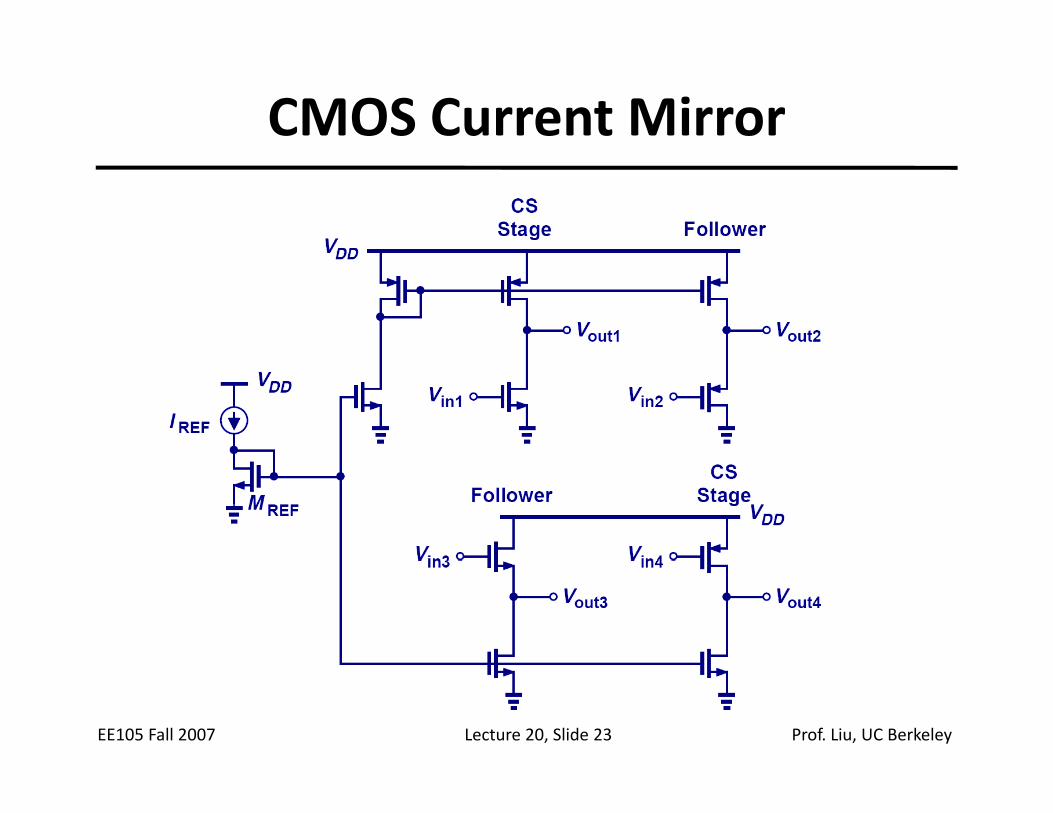
CMOS Current Mirror
EE105 Fall 2007 Lecture 20, Slide 23 Prof. Liu, UC Berkeley